Abstract
This article delves into the capabilities of 3D-printed millimeter-wave (mmWave) layered cylindrical dielectric resonator antennas (CDRAs). The proposed design yielded promising results, boasting a remarkable 53% impedance bandwidth spanning the frequency spectrum from 18 to 34 GHz. Furthermore, the axial ratio (AR) bandwidth achieved an impressive 17%, coupled with a maximum gain of 13.3 dBic. These notable results underscore the efficacy of the proposed design, positioning it as a viable solution for applications in Beyond 5G (B5G). A novel assembly technique was also investigated, employing additive manufacturing to seamlessly merge two layers with distinct dielectric constants into a singular layer. This innovative approach systematically eliminates the potential for air gaps between layers, enhancing the antenna’s overall performance. This approach exhibited potential, particularly in the performance of a millimeter-wave circularly polarized (CP) cylindrical DRA featuring a perforated coating layer. The synergy between measurements and simulations demonstrates a remarkable alignment, providing robust validation of the effectiveness of the proposed design.
1. Introduction
Due to the potential applications in 5G/B5G communication systems, mmWave antennas are receiving increased attention in key technologies such as the Internet of Things (IoT), short-range communications, mobile communications, and imaging systems, among others. However, owing to the shorter wavelength, mmWave signals undergo considerable attenuation losses, which strictly limits their transmission range. However, it is possible to compensate for the attenuation losses by utilizing high-gain antennas or, alternatively, increasing the signal-to-noise ratio and sensitivity of the systems [1]. On the other hand, the commonly used metal antennas are associated with lower efficiencies at the mmWave frequency range due to the increased Ohmic losses. Furthermore, mmWave directive horn antennas suffer from a few drawbacks, including high cost and size, which make them less desirable. Therefore, DRAs represent ideal candidates as they provide enhanced gains, small sizes, different shapes, ease of excitation, low profile, and lightweight qualities [2,3,4]. In addition, DRAs can be easily integrated with electronic circuits due to their mechanical stability and thermal stability. The physical size of an mmWave DRA band is significantly smaller than those working in the microwave band, which creates additional challenges with respect to fabrication tolerance as well as assembly. Nevertheless, various mmWave DRA geometries have been studied recently [1,5,6].
Furthermore, DRA designs with improved impedance bandwidth are required due to the numerous wideband and multiband applications. Broadening bandwidth involves the application of several precepts, including the excitation of multiple resonance modes through proper feeding, layered or stacked DRA configurations [6,7,8]. For example, utilizing multi-modes improves the bandwidths of multilayered and stacked DRAs [7,8]. Nonetheless, overcoming air gaps between the dielectric layers is a substantial challenge. Yet, there is optimism that advanced technologies can mitigate the impact of these air gaps. Customizing DRA geometry through 3D printing, also referred to as additive manufacturing, has garnered significant attention. These innovative processes are known for their accuracy, cost-effectiveness, and efficient, short fabrication cycles.
Following the introduction of 3D printing in the 1980s, several methods were developed, including selective laser sintering, fused deposition modeling (FDM), electron beam melting, binder jetting, material jetting, selective laser melting, and stereo-lithography. These technologies can produce complex, nearly net-shaped parts from polymers, metals, ceramics, and composites. The 3D printing approach is effective in producing high-performance mmWave and terahertz (THz) antennas [9,10,11]. Various antenna geometries have been fabricated using 3D printing technology, such as patch [12], Luneburg lens [13], reflect arrays [14], DRA [15], and integrated lens–DRA configuration [16]. The 3D printing technology can be more effective in eliminating air gaps than other fabrication techniques. Hence, it has recently been considered in the context of a 3D-printed multilayered CDRA that operates over a frequency range of 4.3–8 GHz [17,18].
This paper presents a novel approach to wideband DRAs through 3D printing technology. Traditionally, a two-layer mmWave CDRA is employed, but, here, we propose a transformative replacement: a cylindrical aAlumina structure composed of two sections. The first section constitutes a solid core layer, acting as the DRA, while the second section is a perforated coat layer with a significantly reduced effective dielectric constant. This innovative design is made possible through 3D printing, enabling simultaneous fabrication of both layers without labor-intensive manual assembly and bonding processes. Utilizing the same material for the DRA and the coat further streamlines the printing process, enhancing efficiency. Furthermore, optimization efforts extend beyond fabrication to enhance overall performance. The feed network and coat layer undergo meticulous tuning to improve performance across wide impedance and AR bandwidths, resulting in a notable gain. Validation of our approach is demonstrated through a close agreement between measurements and simulations. It should be noted that regularly shaped mmWave DRAs exhibit inherently delicate and fragile configurations, particularly when designed to operate at higher-order modes. An outer coat serves a dual purpose: improving the antenna’s performance and providing essential structural reinforcement. However, irregularly shaped DRAs pose challenges in this regard, as they are still fragile structures in the absence of the coat, and if added, the role of the coat is unpredictable. Furthermore, conventional DRA geometries align well with 3D printing technology, unlike irregularly shaped counterparts, which may not be as compatible with such manufacturing methods.
The paper is organized as follows: Section 2 details the design and simulation process of the mmWave CDRA, focusing on the two dielectric layers with varying permittivities. Section 3 introduces the design of an equivalent configuration utilizing Alumina for the DRA and coat layer, specifically focusing on the perforation technique employed to achieve the desired dielectric constant. Section 4 presents the empirical measurements, validating our proposed approach, followed by concluding comments in Section 5.
2. Layered CDRA Configuration
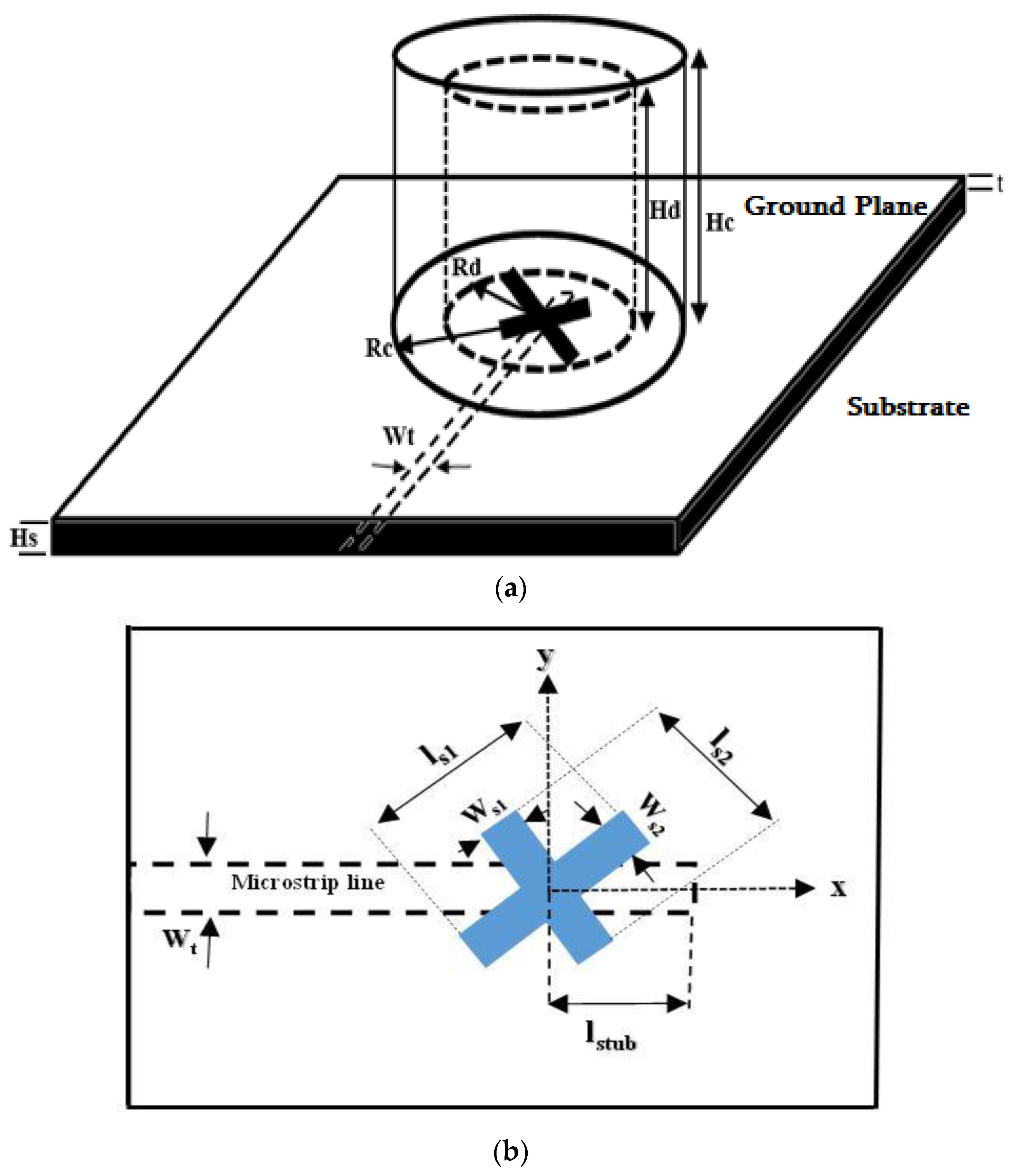
The conventional two-layer cylindrical DRA configuration considered in this study is presented in Figure 1a. The inner layer consists of the cylindrical Alumina DRA fabricated by the T-ceramic, with a loss tangent of 0.002 and a tolerance of 0.05 mm. In contrast to rectangular and hemispherical DRAs, comprehensive design equations for CDRAs are lacking, except for a few applicable to lower-order resonance modes. Numerical tools are commonly employed in literature to design CDRAs operating at higher-order resonance modes. Design equations regarding the coating are also absent, necessitating researchers to rely on optimization techniques. The DRA’s radius and height have been chosen as Rd = 1.5 mm and Hd = 10 mm, respectively. Moreover, an outer layer of polyimide, with a dielectric constant of 3.5, was applied to the DRA. Additionally, the antenna was placed on a copper ground plane of 50 × 50 mm2, located on top of a dielectric substrate measuring 0.42 mm in thickness. The latter was produced using a Rogers material (RO4350B) with a dielectric constant of 3.48 and a loss tangent of 0.0037. Additionally, the ground plane features a cross-slot with unequal arm lengths to induce circularly polarized radiation, as illustrated in Figure 1b. The lengths of these cross-slot arms have been finely tuned to ls1 = 1.77 mm and ls2 = 2.85 mm, each with a width of Ws1 = Ws2 = 0.45 mm. The cross-slot is accompanied by an open stub length of 1.27 mm for optimal impedance matching and is positioned at a 45° angle relative to a 50 Ω microstrip line. This setup excites two nearly degenerate DRA modes with equal amplitude and in quadrature, resulting in circular polarization. Specifically, the modes HE117 at 24 GHz, HE119 at 29 GHz, and HE11,11 at 32.5 GHz have been effectively generated. The simulations were carried out using the CST time domain solver.

Figure 1.
The configuration of (a) the layered CDRA and (b) the cross-slot.
The CST time domain solver is advantageous for wide frequency range calculations as it necessitates only one simulation, with the frequency response derived using the fast Fourier transform (FFT). The time domain solver also allows spectrum calculation with arbitrarily fine frequency resolution without extra effort, making it more suitable for simulating electrically large structures. Conversely, the frequency domain method requires discrete simulations at specified frequencies with a defined frequency step to cover the entire operating bandwidth [19]. Moreover, DRAs often involve transient electromagnetic phenomena due to the interaction between the electromagnetic waves and the dielectric material. Time domain analysis can capture these transient effects more accurately, making it suitable for modelling DRAs.
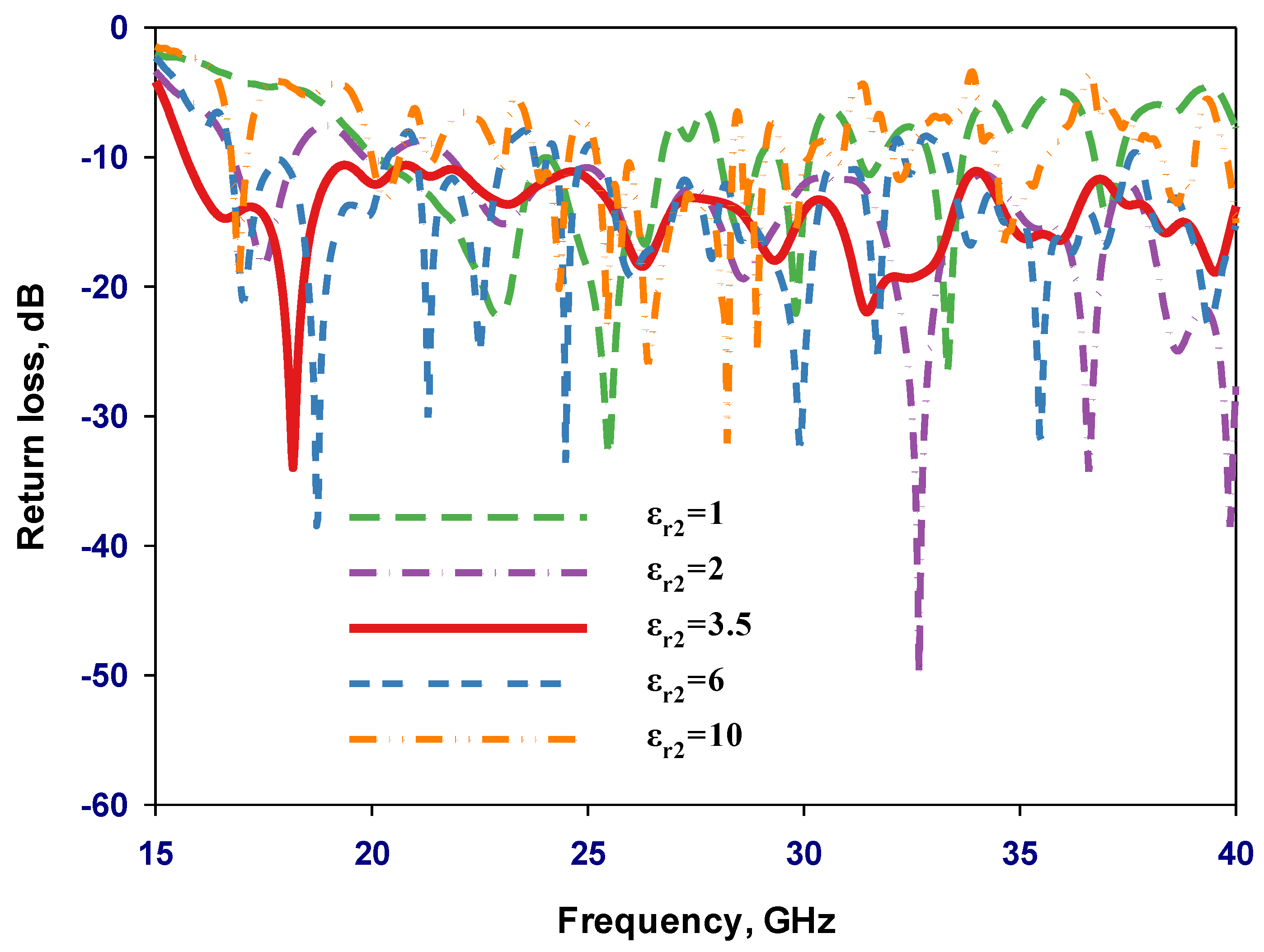
A parametric study was undertaken to identify the optimal parameters for achieving wide impedance and axial ratio bandwidths at Hc = 12.15 mm. The study focused on determining the ideal values for the outer layer radius (Rc) and dielectric constant (εr2). A range of outer layer radii was initially considered, including Rc = 12.5, 8, 5.5, and 3 mm. For each specific Rc value, εr2 was systematically optimized as illustrated in Figure 2, Figure 3 and Figure 4. Figure 2 illustrates a noteworthy achievement—a wide impedance bandwidth of 88% was attained when εr2 was set to 3.5. This bandwidth surpassed those observed with εr2 = 2, 6, and 10. The impedance bandwidth expanded for εr2 = 3.5 because the outer layer functions as an optimized transition medium between the DRA and free space [20], which minimizes reflections at the DRA–air interface, contributing to improved impedance-matching bandwidth.
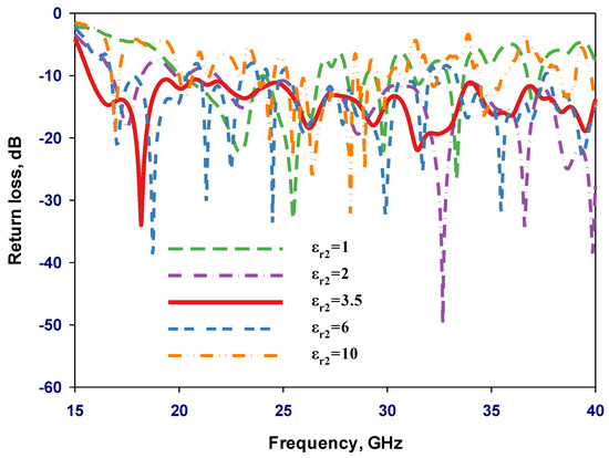
Figure 2.
Simulated return losses using various outer layers’ dielectric constants, εr2.
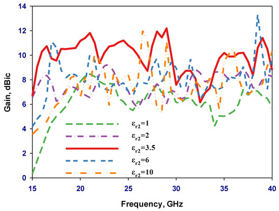
Figure 3.
Simulated gain using various outer layers’ dielectric constants, εr2.
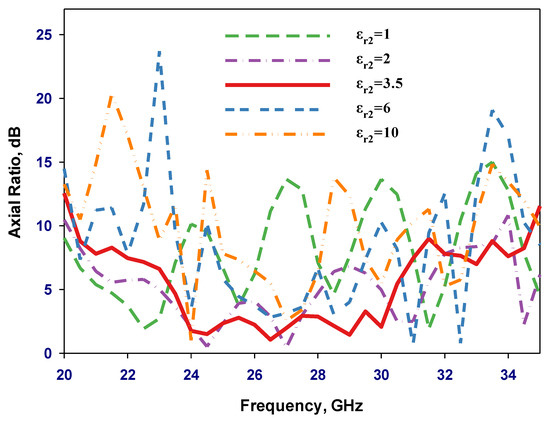
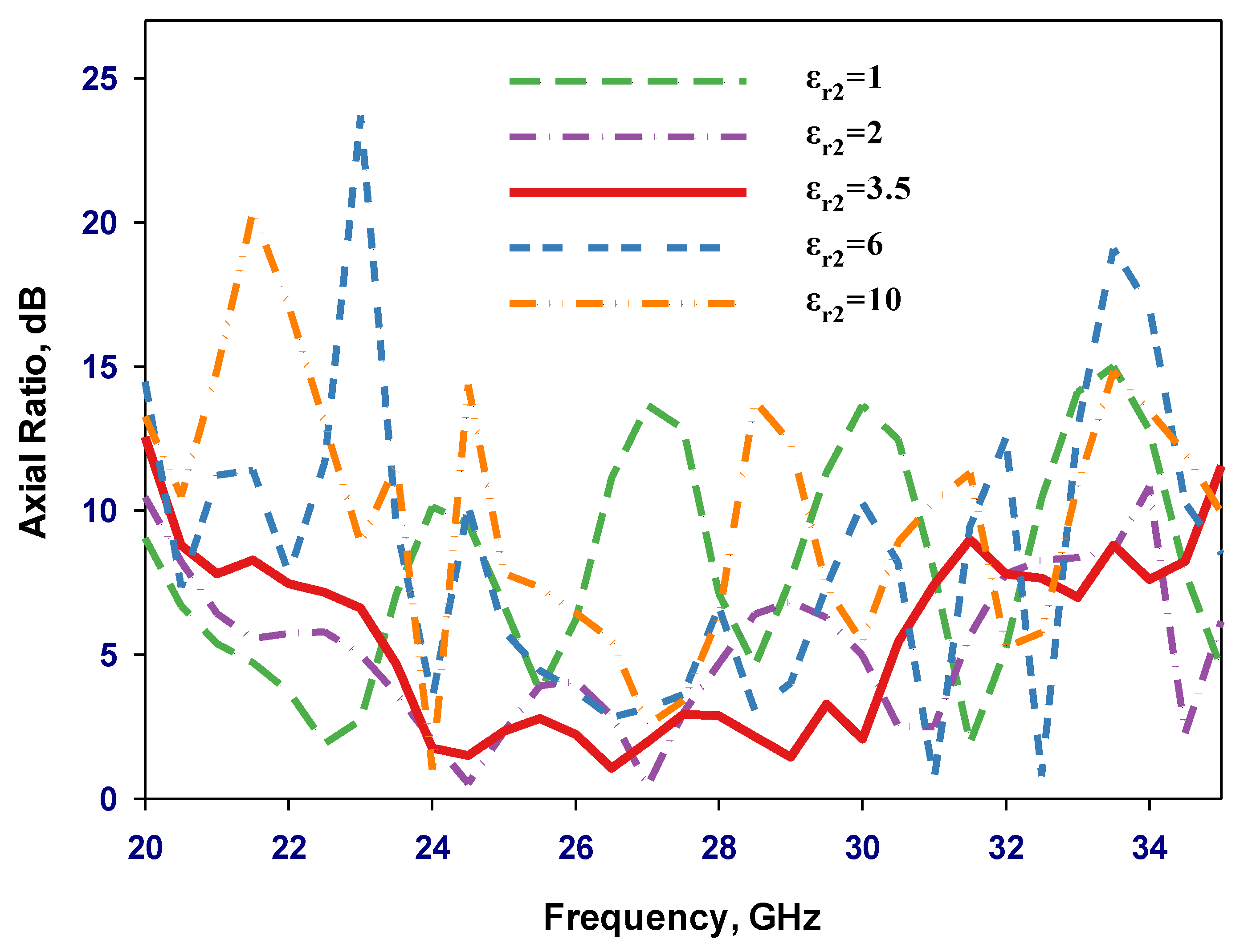
Figure 4.
Simulated axial ratio using various outer layers’ dielectric constants, εr2.
Moreover, the coat’s presence also reduces the configuration’s effective permittivity, enhancing bandwidth. Increasing the relative permittivity of the external layer requires a consequent reduction in its optimal radius. Specifically, when the relative permittivities were set to 2, 3.5, 6, and 10, the corresponding optimal Rc values were 12.5, 8, 5.5, and 3 mm, respectively. Importantly, this pattern is consistent with previous studies [21], which reported a wider impedance bandwidth when the external layer’s dielectric constant is approximately half that of the original DRA. In addition, when the relative permittivity εr2 was set to 3.5 and Rc = 8 mm, the antenna exhibited exceptional performance, achieving a remarkable gain of 12.29 dBic and an impressive axial ratio bandwidth of 23.3%. In contrast, under conditions where εr2 was increased to 6, the antenna demonstrated lower characteristics, with a gain dropping to 9.6 dBi and a significantly reduced axial ratio bandwidth of only 0.93%. Moreover, Figure 3 demonstrates rapid variations in gain that can be attributed to weakly coupled resonance modes in the DRA. These resonance modes, being weakly coupled, respond sensitively to changes in frequency or other parameters, leading to the observed rapid fluctuations in gain. The broad frequency range in which these resonance modes operate makes the antenna’s gain susceptible to rapid changes. Without the dielectric coat, the highest gain was achieved at 22 GHz with the excitation of the HE115 resonance mode. Table 1 summarizes the optimum antenna performances for various coating layer radii and dielectric constant combinations.

Table 1.
Optimum parameters of the coat layer.
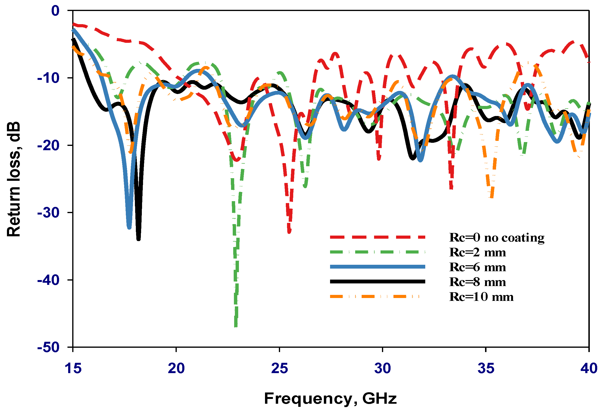
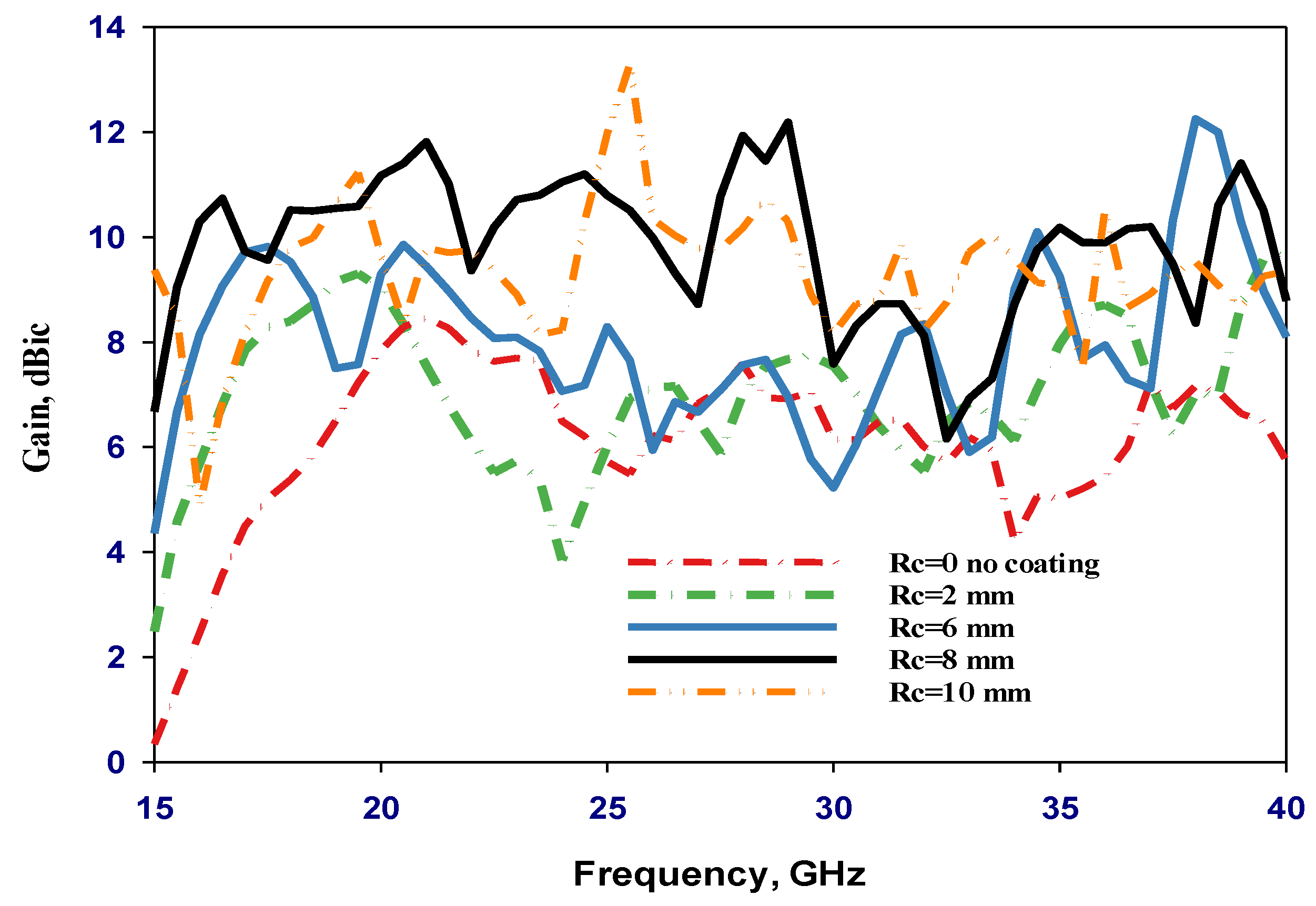
The impact of the outer coat layer radius, Rc, has also been investigated, as illustrated in Figure 5, Figure 6 and Figure 7 when εr2 = 3.5. These results confirm that an optimum outer layer radius of 8 mm offers the widest impedance, AR bandwidths, and gain compared to 28.6%, 3.6%, and 7.64 dBic, respectively, for a single-layer DRA configuration. The broad bandwidth is brought on by multi-mode excitation at nearby resonance frequencies, where the adjacent individual bandwidths are merged. The gain has been increased due to exciting the higher order modes of HE115, HE117, HE119, HE11,11, HE11,13, and HE11,15 at 18 GHz, 22 GHz, 29 GHz, 32.5 GHz, 36 GHz, and 40 GHz, respectively, rather than just the respective modes of HE115 and HE117 at 23 GHz and 25.5 GHz in the case of a single-layer antenna. It is worth mentioning that when adding the coat, the higher order modes are associated with confined electromagnetic fields together with an increased number of short magnetic dipoles inside the DRA, which results in a higher gain. Using a material with higher permittivity can store more energy because the DRA radiates across the entirety of its surface, barring the grounded area [21]. However, this can lead to a narrower bandwidth. Hence, low-permittivity material is employed for the outer layer to counteract this. In such a configuration, coating lessens the sudden permittivity shift between the DRA and air [20]. Consequently, the DRA structure endures more radiation loss, leading to a broader impedance bandwidth.
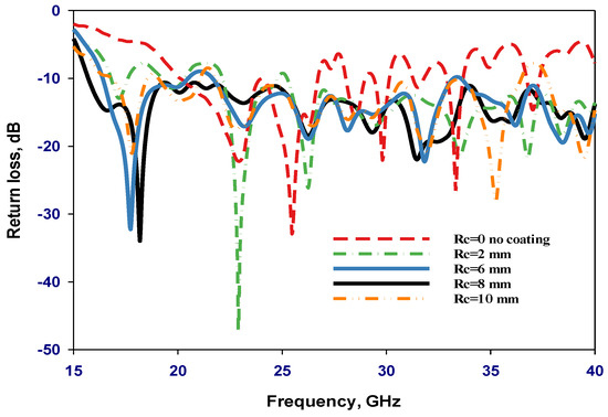
Figure 5.
Simulated return losses with various outer layers’ radii when εr2 = 3.5.
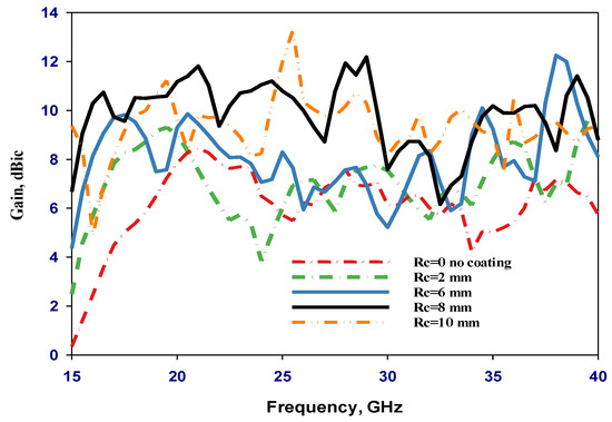
Figure 6.
Simulated realized gain with various outer layers’ radii when εr2 = 3.5.
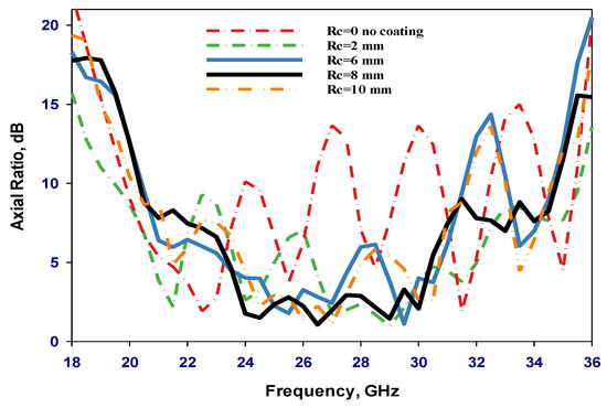
Figure 7.
Simulated axial ratio with various outer layers’ radii when εr2 = 3.5.
Figure 8 depicts simulated distributions of H-field and E-field for different excited modes within the specified CP two-layer cylindrical DRA at various targeted frequencies. These distributions, obtained through the CST Eigenmode solver, are illustrated across multiple planes of the resonator. The results distinctly demonstrate the presence of the required modes within the cylindrical DRA.
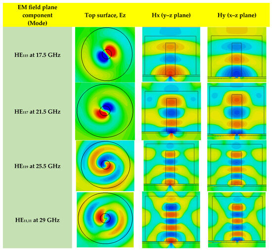
Figure 8.
Electric and magnetic field distributions inside circularly polarized cylindrical DRAs.
3. Perforated CDRA Configuration
As previously highlighted, multilayer DRA configurations are burdened with notable constraints at mmWave frequencies, such as augmented physical dimensions and the requirement for sophisticated assembly processes. These processes encompass the bonding of distinct dielectric layers in a manner that should eliminate any potential air gaps. This study endeavours to tackle this predicament by deploying 3D printing technology to fabricate an Alumina-based perforated DRA structure. Consequently, using an automated 3D printing process, the antenna prototype can be measured without requiring any time-consuming manual assembly and bonding processes. Furthermore, using the same material for the DRA and the coat simplifies and expedites the 3D printing. The proposed configuration has been fabricated by using the FDM 3D printing technique. The central section consists of a solid Alumina, representing the actual DRA, and a perforated Alumina coat layer with a reduced effective dielectric constant was utilized instead of the solid outer polyimide coat. The proposed mmWave cylindrical DRA and coat configuration become easier to fabricate. Additionally, different effective dielectric constants of the coating layer can be achieved by varying the hole sizes in accordance with filling-ratio theory [13,18]. As demonstrated in Figure 9, the proposed 3D-printed layered CDRA comprises two concentric dielectric sections: a solid cylindrical DRA in the center and an outer section with different air-filling ratios, providing different effective dielectric constants, εeff. The proposed antenna is configured using the dimensions and feed network described in the previous section, including the cross-slot. To create the perforated coat, a single material with a dielectric constant of 10 ± 0.35 over 17.7–30 GHz has been used to 3D-print the inhomogeneous antenna configuration. The εeff value can be calculated using [5]
whereby an Alumina cubic unit was introduced. The cell thickness tc determined εeff and the side length was fixed at 1.63 mm. The proposed configuration is presented in Figure 10 with a perforated dielectric coat. The geometrical parameters of the DRA with perforated coat are listed in Table 2.
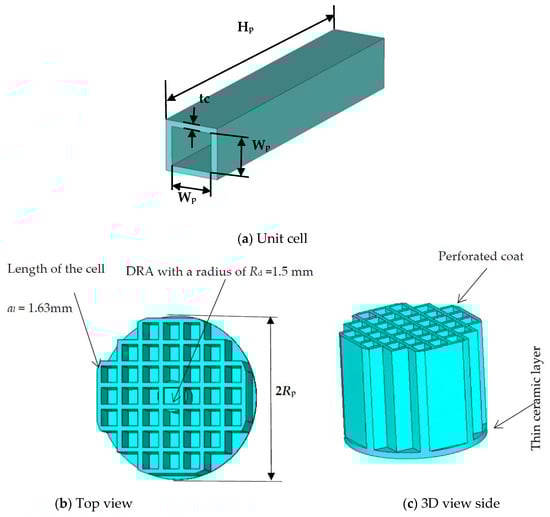
Figure 9.
Cylindrical DRA with a perforated dielectric coat.
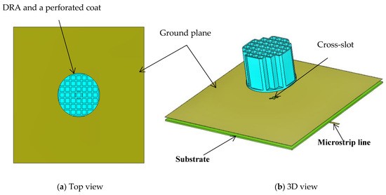
Figure 10.
The configuration of the cylindrical DRA with a perforated dielectric coat.
Table 2.
The parameters of the proposed antenna with a perforated coat.
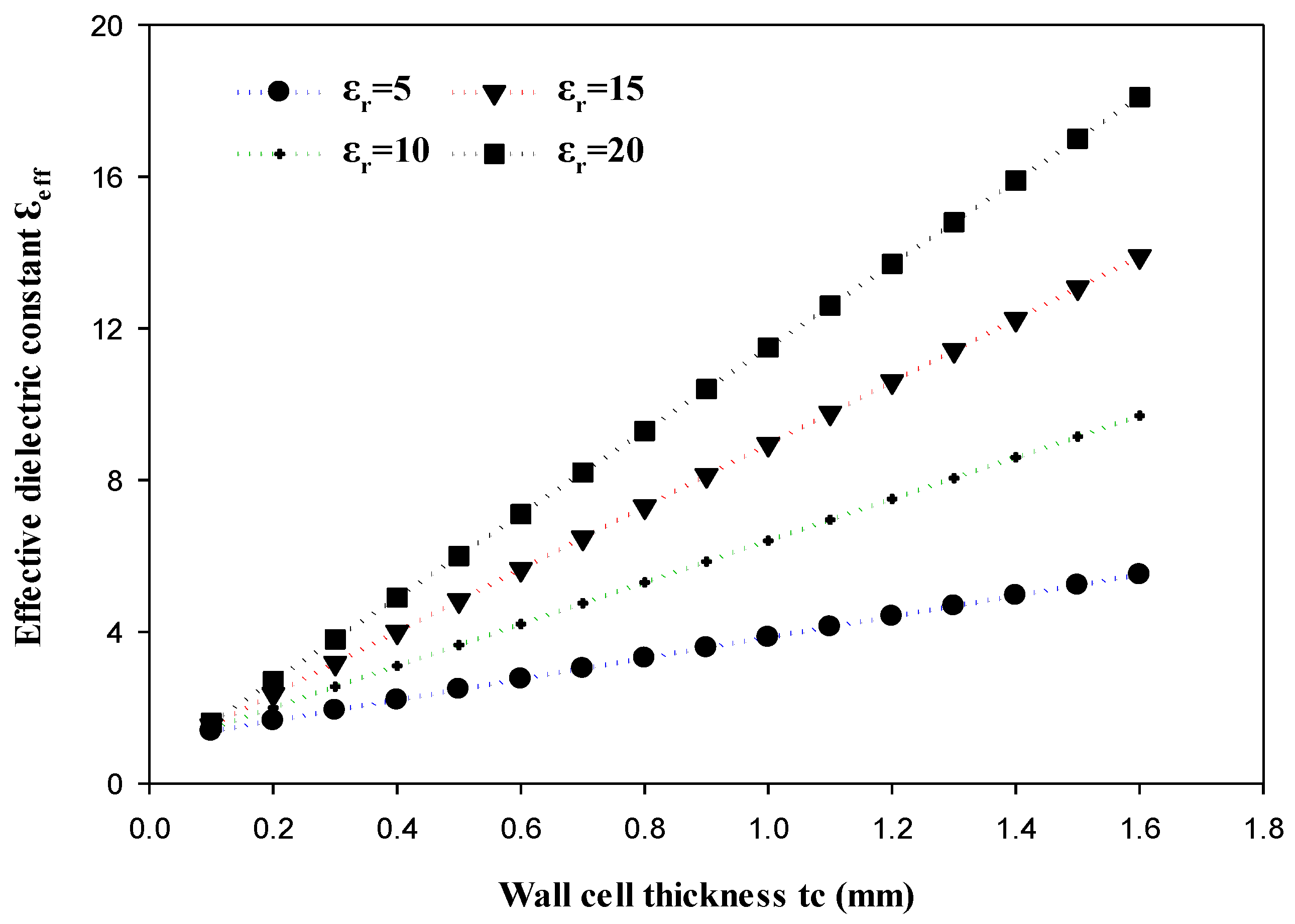
Three-dimensional printable unit cells have several advantages, including modifying the wall thickness to regulate the effective dielectric constant, as per filling-ratio theory [7]. A fixed dielectric constant for each layer characterizes the CDRA with a perforated Alumina coat, as presented in Figure 10. As a result, each layer’s unit cells have equivalent wall thicknesses. In addition, these unit cells can physically support each other, with no additional supporting material requirements during 3D printing. Consequently, printing time and material costs have decreased significantly. It should be noted that for easy detachment from the building platform, a thin dielectric layer with a thickness of 0.5 mm and a radius of 8 mm was printed underneath the DRA as well as improving the matching since the wall thickness affects the effective permittivity of a perforated dielectric coat. Figure 11 demonstrates the variation of εeff as a function of tc for a variety of printing materials of εr = 5, 10, 15, and 20, where it can be noted that when εr = 10, an effective dielectric constant of 3.6 is achieved using tc = 0.49 mm. Also, the required effective dielectric constant can be attained by properly choosing the material and unit cell thickness. However, this depends on the materials availability and the minimum unit cell thickness that can be 3D-printed.
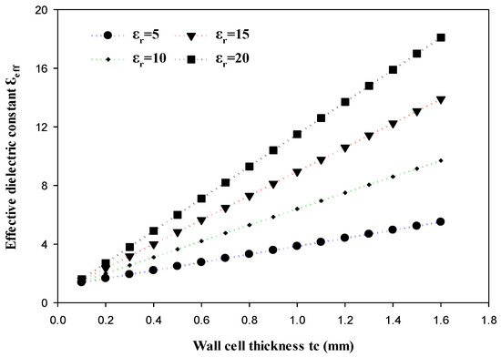
Figure 11.
Perforated cylindrical layer effective permittivity as a function of tc.
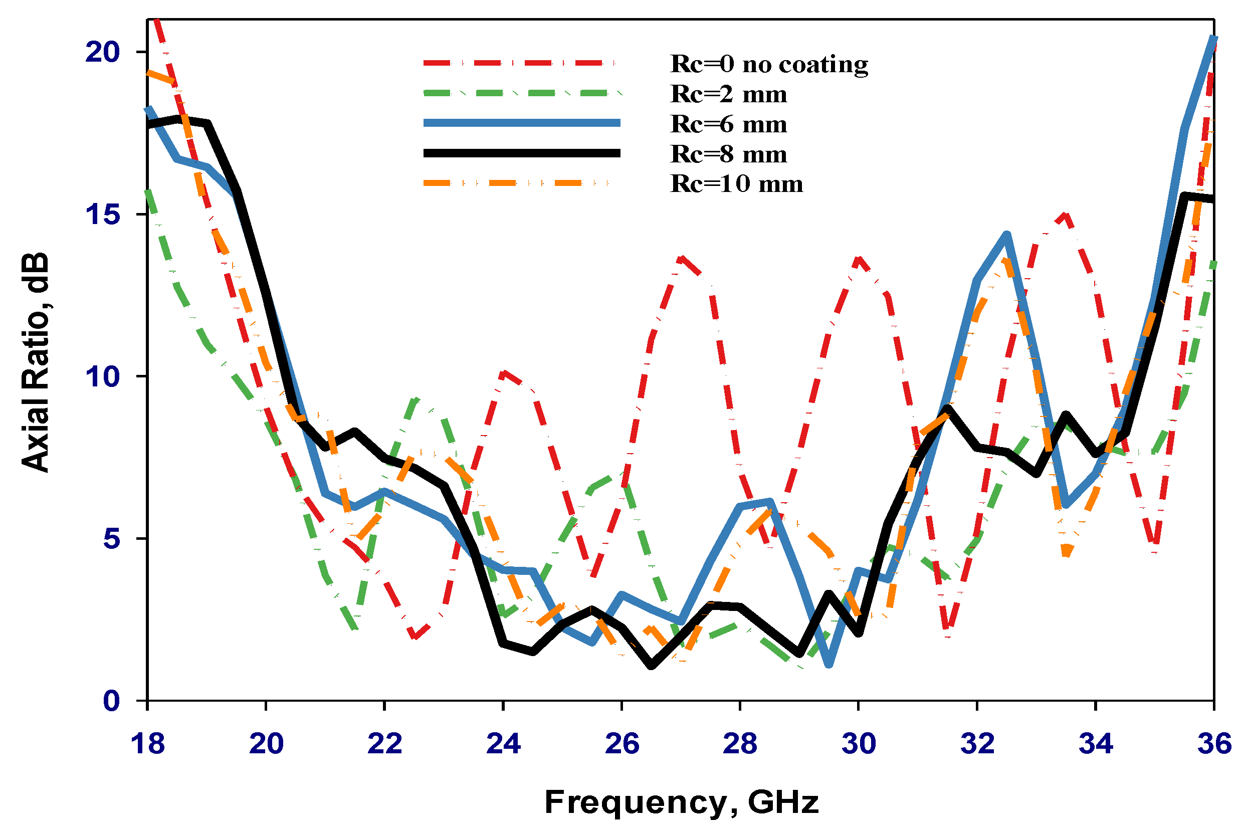
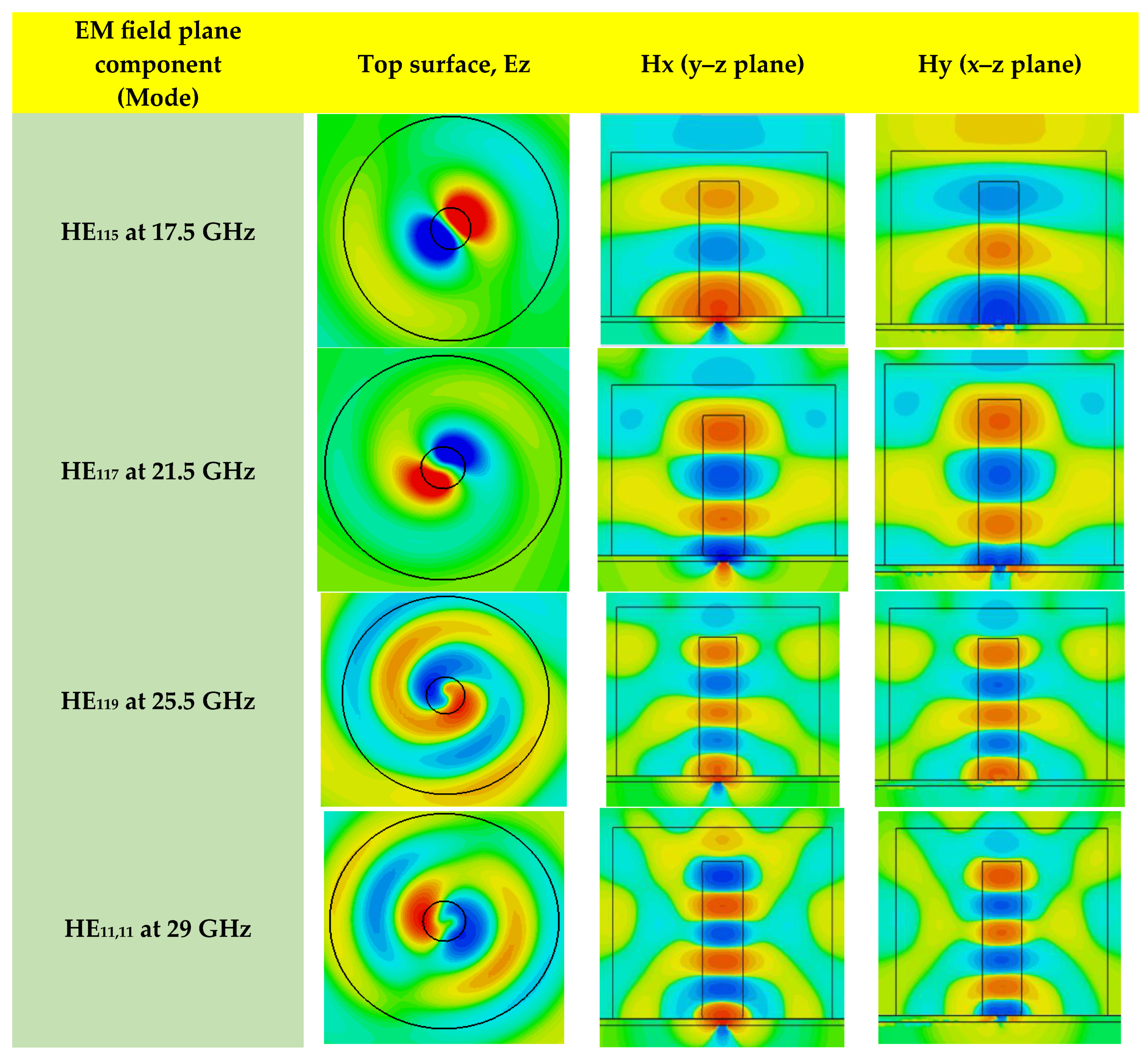
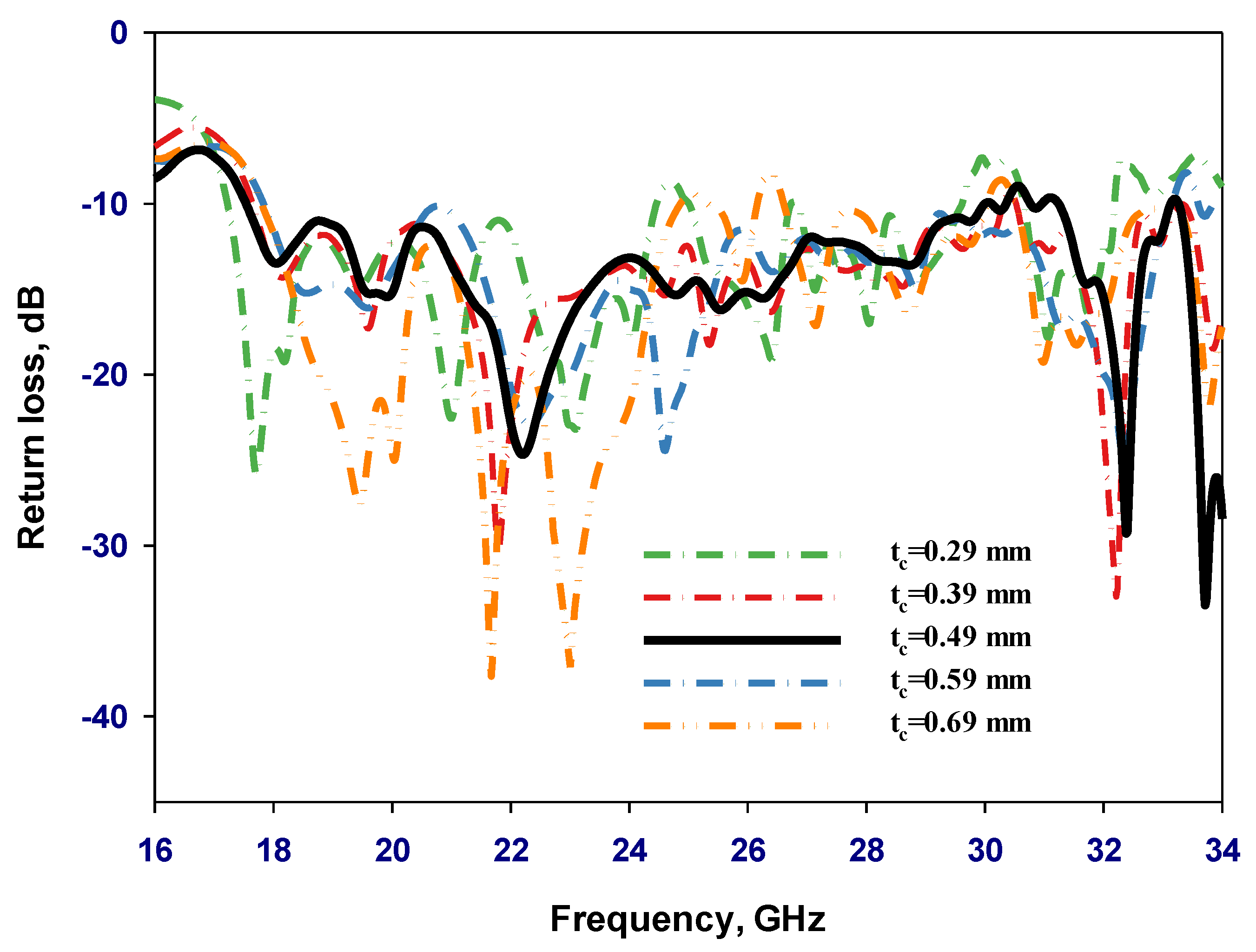
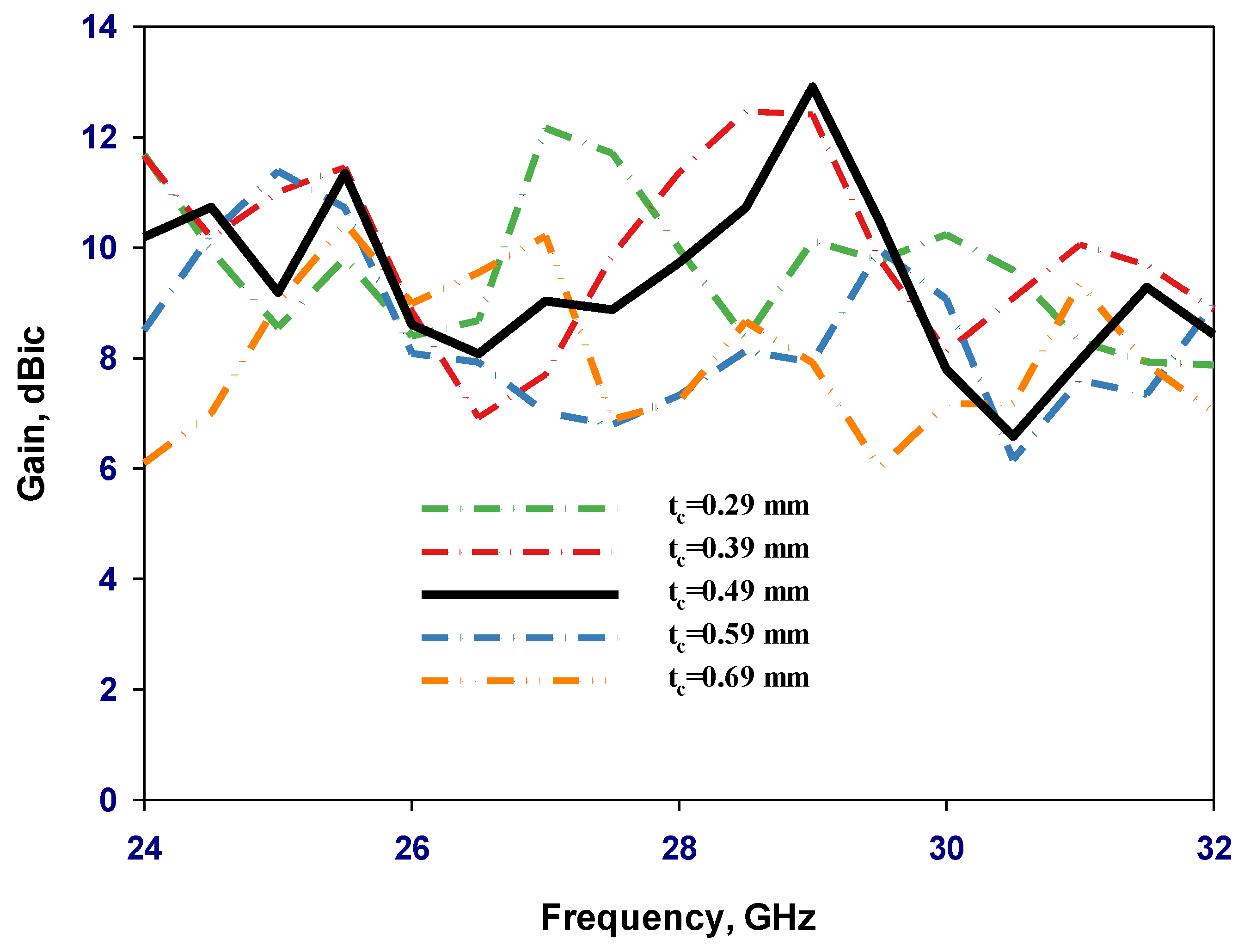
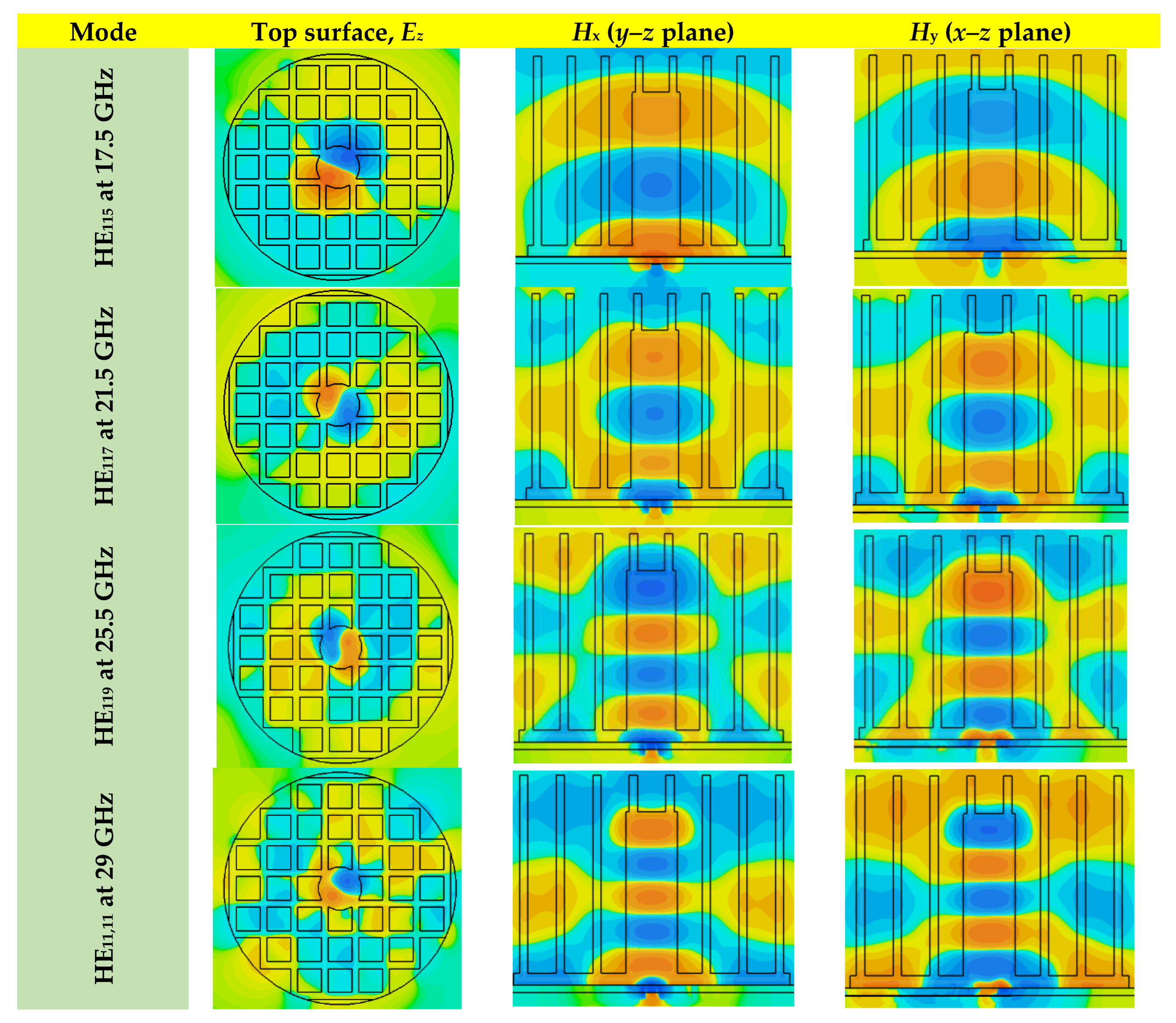
Figure 12 illustrates the reflection coefficient variation as a function of the unit cell wall thickness using the feeding cross-slot of the previous section and εr = 10. From these results, it can be noted that the lowest impedance bandwidths of 32.2% have been achieved using a wall thickness of tc = 0.69 mm, corresponding to an effective dielectric constant of 4.35, where only two resonance modes, HE115 and HE117, have been excited. Such a thickness has also provided the narrowest AR bandwidth, 1.6%, as illustrated in Figure 13, and a realized gain of 8 dBic at 29 GHz as demonstrated in Figure 14. Furthermore, when tc =0.49 mm, it was possible to attain a considerably broader impedance, axial ratio bandwidths, and gain of 53.3%, 16.3%, and 13.13 dBic, respectively, due to the excitation of the several resonance modes. It can be observed that the achieved optimum impedance and AR bandwidths are narrower than those of a conventional layered DRA with two different dielectric layers presented in the previous section. This can be attributed to the fact that the same feed networks, with identical cross-slots, have been utilized in both configurations even though the coating layer dielectric constant has changed from 3.5 in the former configuration to 3.6 in the 3D-printed counterpart, which necessitates the re-design of the feed network. However, this would have resulted in a configuration with different fabrication technologies and feeding networks, which may result in a questionable comparison of the performance of the two DRAs. The simulated H-field and E-field distributions inside the DRA for various excited resonance modes are illustrated in Figure 15. It can be observed that the following modes are supported: HE115, HE117, HE119, and HE11,11 at 17.5 GHz, 21.5 GHz, 25.5 GHz, and 29 GHz, respectively. These results have been achieved using the CST Eigenmode solver for an isolated DRA and the excitation has been confirmed by a cross-slot-fed DRA.
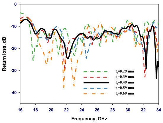
Figure 12.
Simulated |S11| for cylindrical DRAs with a perforated coat layer and various tc values.
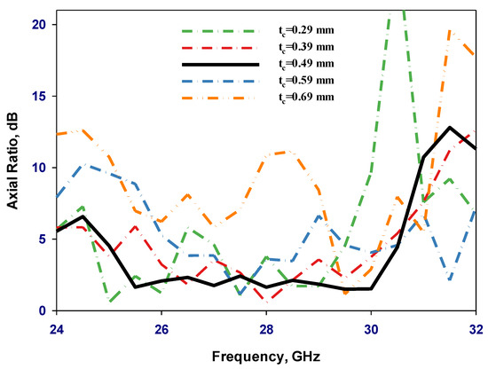
Figure 13.
Simulated axial ratio for cylindrical DRAs with a perforated coat layer and various tc values.

Figure 14.
Simulated gain for cylindrical DRAs with a perforated coat layer and various tc values.
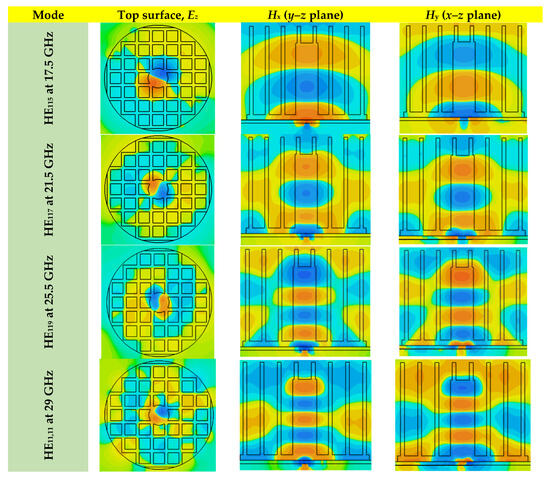
Figure 15.
Electric and magnetic field distributions inside a CDRA with a perforated layer.
4. Measurements
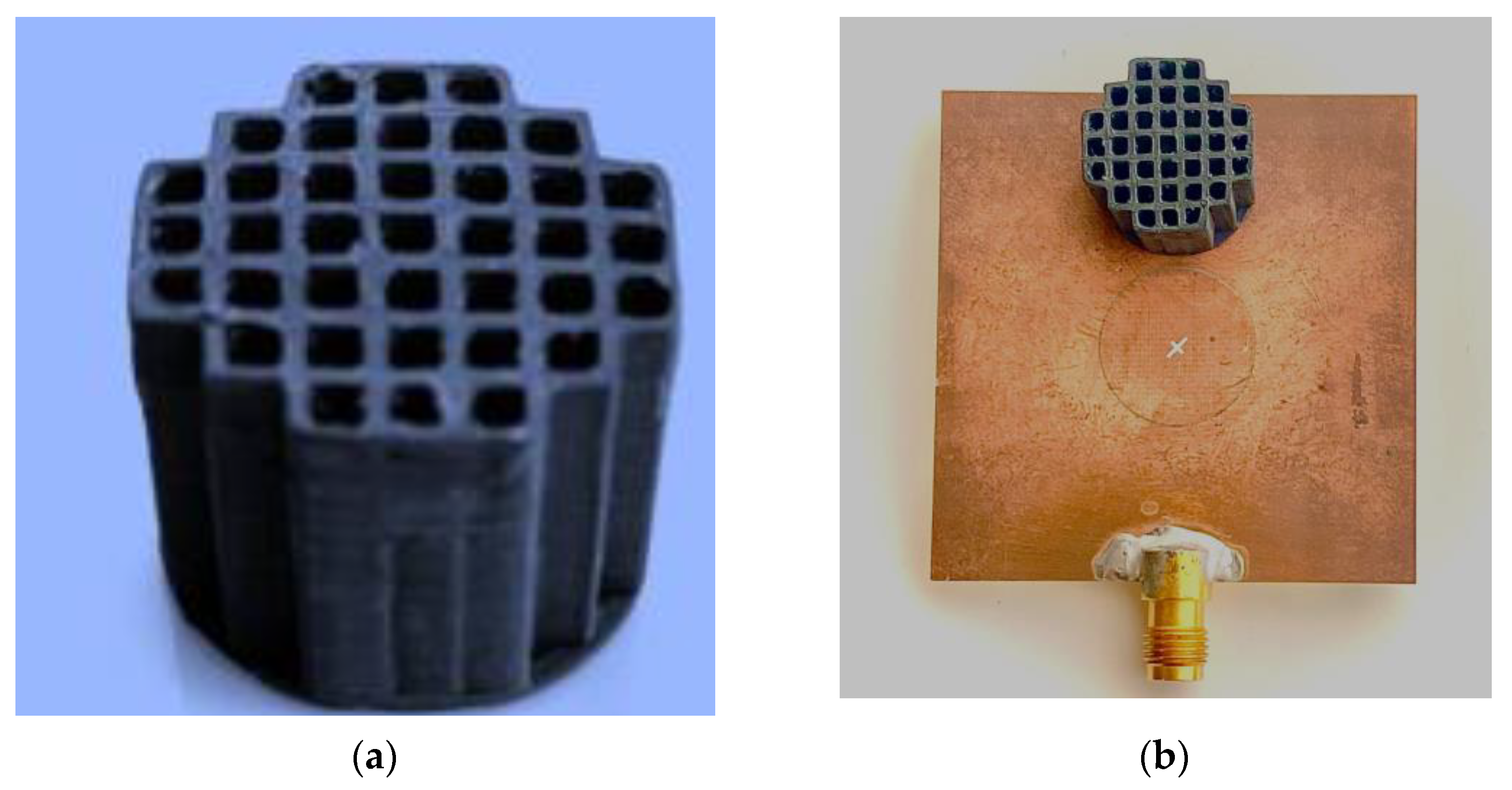
A prototype of a cylindrical DRA with a perforated coat layer is illustrated in Figure 16, where the DRA and coat have been 3D-printed using Alumina by the 3D Matters company [22]. The proposed antenna has been mounted onto a feed network fabricated by Wrekin Circuits. The feed network consists of a Ro4350B Rogers dielectric substrate with a thickness of 0.42 mm, a relative permittivity of 3.48, and a loss tangent of 0.0037. A microstrip line was printed under the Rogers substrate. Additionally, a 2.4 mm SMA connector connects to microstrip line feeding and an Agilent Technologies E5071C mmWave vector network analyzer has been connected using a 50 Ω coaxial cable [23].

Figure 16.
(a) Prototype with perforated coat layer and (b) feed network with outlined DRA position.
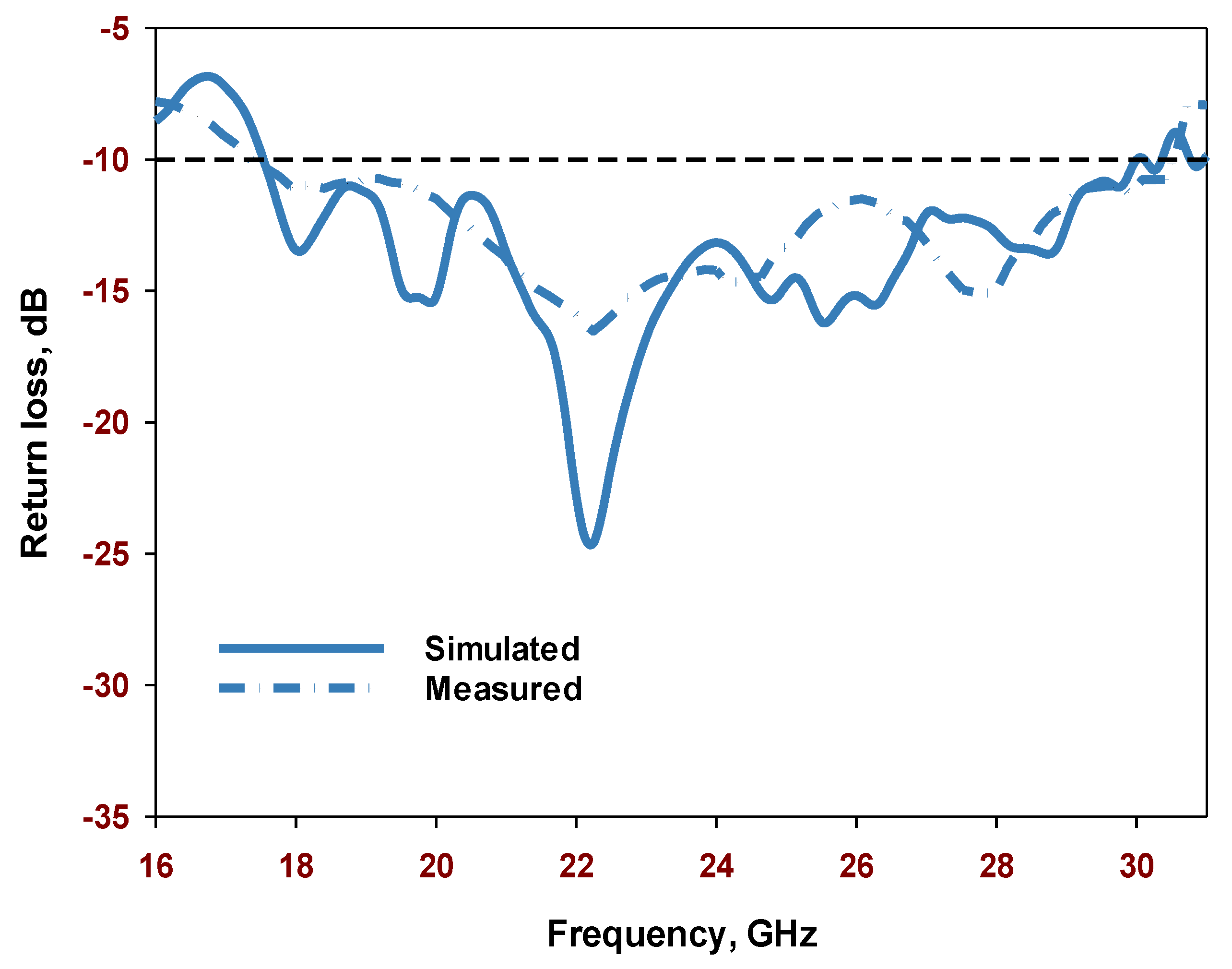
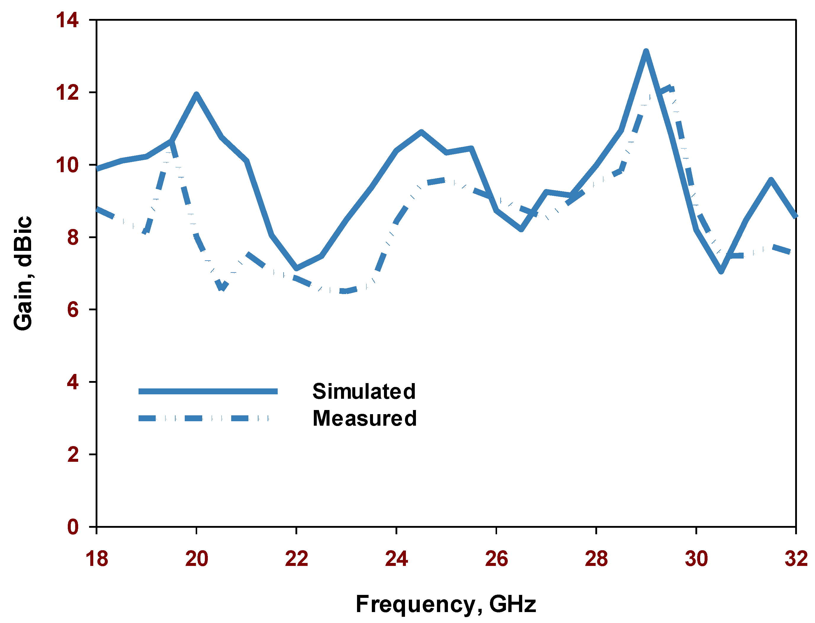
A comparison between the simulated and measured return losses is illustrated in Figure 17. Simulated impedance bandwidth of 52.6% has been achieved, which covers a frequency range of 17.5 GHz to 30.5 GHz, comparing well to a measured bandwidth of 53.3%, which covers a frequency range of 17.4 GHz to 30.3 GHz. The marginal discrepancy between the simulated and measured results can be attributed to the uncertainties in the effective dielectric constant of the prototype as well as measurement errors. The wide bandwidth can be attributed to the excitation and the merging of multiple hybrid modes. Furthermore, the simulated and measured realized gains are presented in Figure 18, where it can be observed that the maximum measured and simulated gains are 12 dBic and 13.3 dBic, respectively, when the HE11,11 resonance mode is excited at 29 GHz. It is worth pointing out that a realized gain of 13.3 dBic represents one of the highest reported gains from a single DRA and it is comparable to that of an array, albeit using a single DRA and without the need for a complex feeding network.

Figure 17.
Simulated and measured reflection coefficients of the perforated configuration.
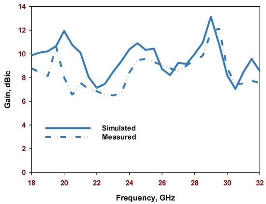
Figure 18.
The simulated and measured gains of the perforated antenna configuration.
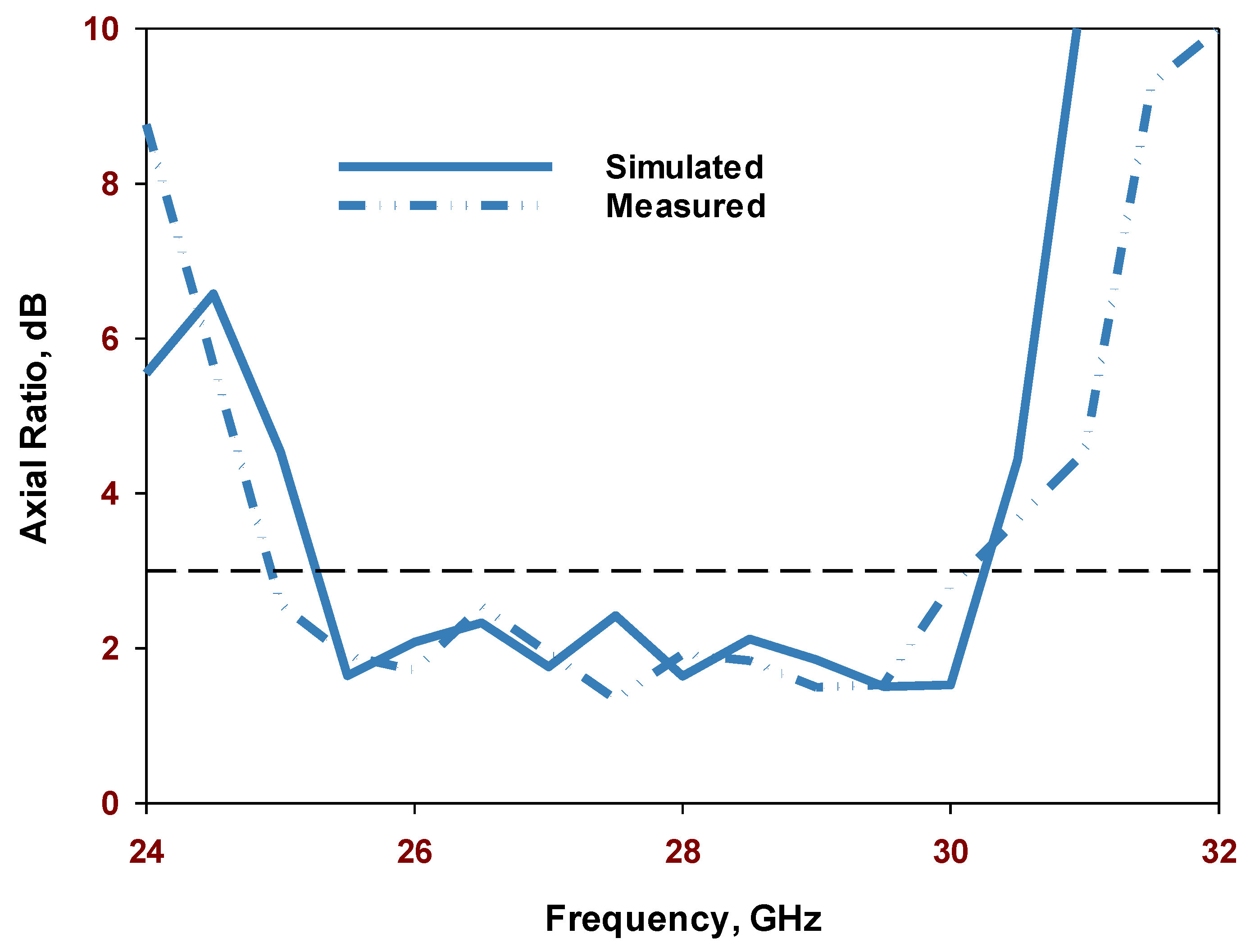
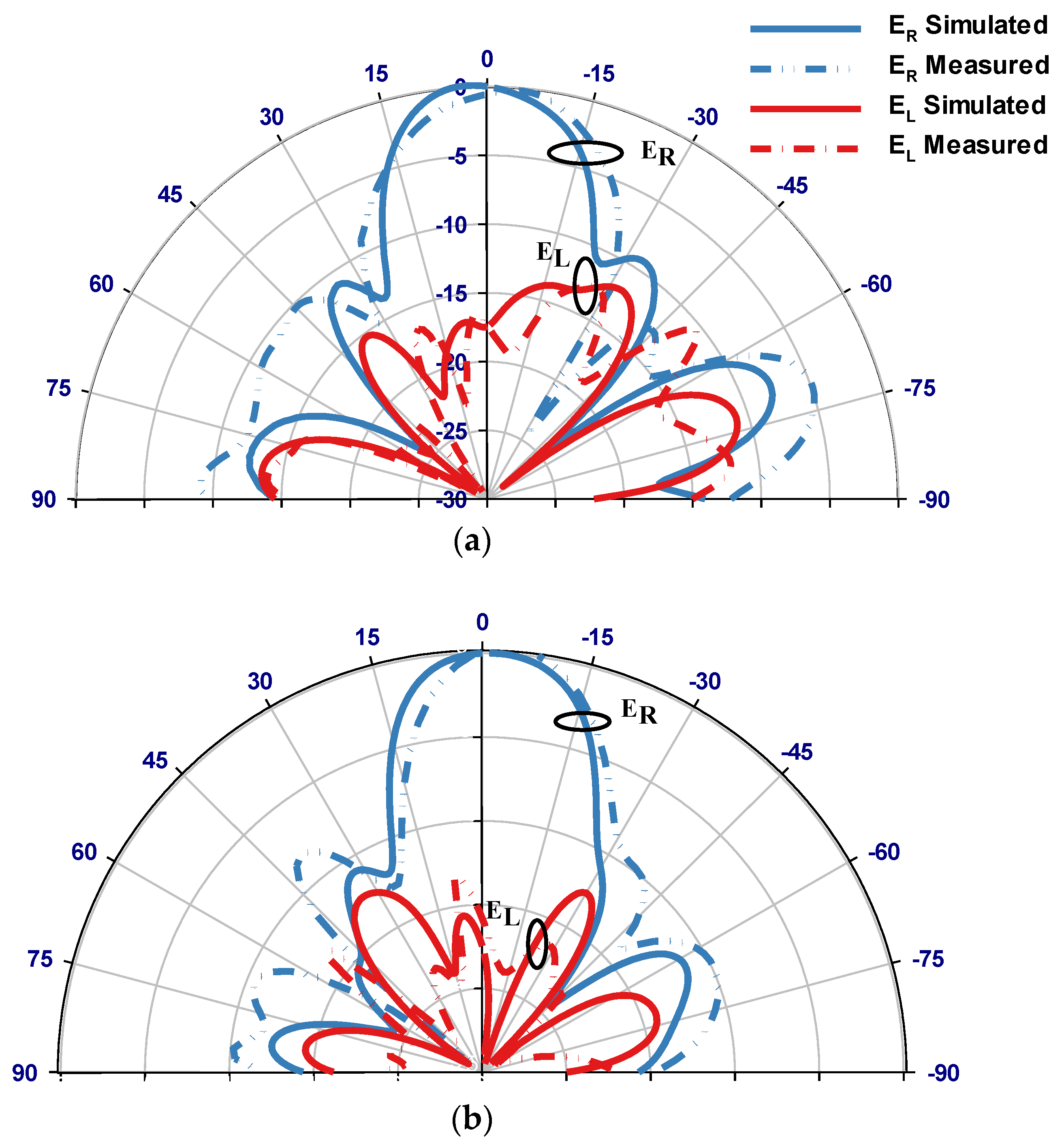
The simulated and measured boresight axial ratios are presented in Figure 19, with good agreement between the 3dB axial ratio bandwidths of 17% and 16.5%, respectively. The measured and simulated radiation patterns of the proposed circularly polarized antenna are presented in Figure 20, where the HE11,11 mode is excited at 29 GHz. The patterns agree reasonably with each other and demonstrate a right-hand CP radiation since the electric field component ER is greater than EL by almost 12 dB. The measurements closely match the simulations throughout the achieved bandwidth with expected experimental errors at the considered frequency range. Contributing factors to these errors are possible discrepancies between practical and ideal dielectric properties, soldering of SMA connectors, and the meticulous alignment of the DRA during measurements.

Figure 19.
The simulated and measured axial ratios of the perforated antenna configuration.
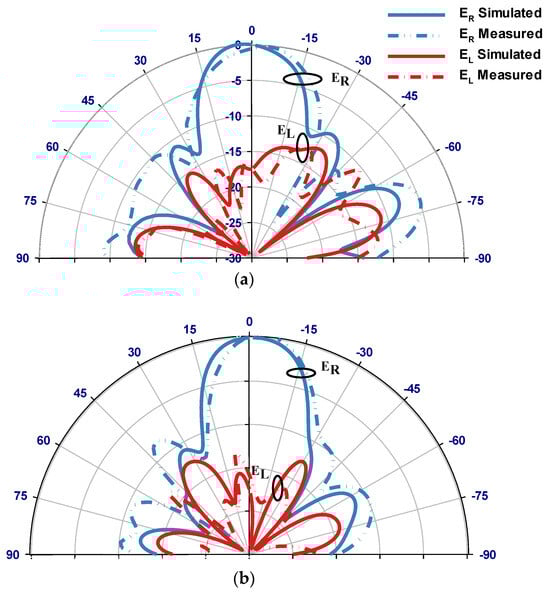
Figure 20.
Simulated and measured radiation patterns at 29 GHz: (a) ϕ = 0° and (b) ϕ = 90°.
Table 3 illustrates a comparison between the performance of the proposed perforated antenna and other perforated designs, where the outperformance of the proposed configuration is evident in terms of the CP radiation and a considerably higher gain. In addition, the achieved impedance bandwidth is comparable to those reported in the literature. Anyway, this study addressed the challenge of designing an mmWave layered CDRA with physically small dimensions compared to those reported earlier utilizing considerably larger physical dimensions.
Table 3.
Proposed antenna performance compared to previously reported designs.
5. Conclusions
This study has examined the possibility of assigning a single dielectric material to a 3D-printed layered CDRA operating in the mmWave frequency band. Two identical DRA configurations have been considered: a conventional two-layer DRA and an equivalent 3D-printed counterpart. In the latter configuration, Alumina has been utilized for the two layers, albeit with a reduced dielectric constant perforated segment that acts as a coating layer. This facilitates automated assembly and bonding of the relatively complex layered DRA, eliminating potential air gaps between the dielectric layers. The equivalent single-material CDRA configuration provided measured impedance bandwidth of 53.3% and an axial ratio of 17% with a maximum realized gain of 12.5 dBic at 29 GHz. The measured results demonstrate a close agreement with the simulated counterpart. The achieved attractive features are useful for B5G applications requiring antennas with high gain and wide bandwidth. The two considered structures have utilized identical physical dimensions for a valid comparison. However, the effective dielectric constant of the perforated layer is ~3.6 compared to 3.5 for the pPolyimide coating layer. Therefore, even wider impedance and axial ratio bandwidths are expected to be achieved by optimizing the feeding cross-slot of the antenna configuration with a perforated coating.
Author Contributions
W.A.: conceptional design, simulation, measurements, writing—original draft; R.A.: writing—review and editing, investigation; T.S.A.: validation; Y.K.: methodology; S.K.K.: supervision and writing. All authors have read and agreed to the published version of the manuscript.
Funding
This research received no external funding.
Institutional Review Board Statement
Not applicable.
Informed Consent Statement
Not applicable.
Data Availability Statement
Data are contained within the article.
Acknowledgments
The authors acknowledge using the National mmWave Facility and thank Steve Marsden for supporting the measurements.
Conflicts of Interest
The authors declare no conflicts of interest.
References
- Kesavan, A.; Al-Hassan, M.A.; Ben Mabrouk, I.; Denidni, T.A. Wideband circular polarized dielectric resonator antenna array for millimeter-wave applications. Sensors 2021, 21, 3614. [Google Scholar] [CrossRef] [PubMed]
- Leung, K.W.; Long, S.A. Overview of the Dielectric Resonator Antenna. In Dielectric Resonator Antennas; Research Studies Press: Baldock, UK, 2003; pp. 1–47. [Google Scholar]
- Petosa, A.; Thirakoune, S. Rectangular dielectric resonator antennas with enhanced gain. IEEE Trans. Antennas Propagat. 2011, 59, 1385–1389. [Google Scholar] [CrossRef]
- Gangwar, R.K.; Singh, S.; Kumar, D. Comparative studies of rectangular dielectric resonator antenna with probe and microstrip line feeds. Arch. App. Sci. Res. 2010, 2, 1–10. [Google Scholar]
- Abdou, T.S.; Khamas, S.K. Millimeter wave dielectric resonator antenna for off-body communications with grooved ground plane. In Proceedings of the 2023 International Workshop on Antenna Technology (iWAT), Aalborg, Denmark, 15–17 May 2023; pp. 1–4. [Google Scholar] [CrossRef]
- Alanazi, M.D.; Khamas, S.K. Wideband mm-wave hemispherical dielectric resonator antenna with simple alignment and assembly procedures. Electronics 2022, 11, 2917. [Google Scholar] [CrossRef]
- Abdulmajid, A.A.; Khalil, Y.; Khamas, S. Higher-order-mode circularly polarized two-layer rectangular dielectric resonator antenna. IEEE Antennas Wirel. Propag. Lett. 2018, 17, 1114–1117. [Google Scholar] [CrossRef]
- Sun, W.-J.; Yang, W.-W.; Chu, P.; Chen, J.-X. Design of a wideband circularly polarized stacked dielectric resonator antenna. IEEE Trans. Antennas Propagat. 2019, 67, 591–595. [Google Scholar] [CrossRef]
- Zhang, B.; Guo, Y.-X.; Zirath, H.; Zhang, Y.P. Investigation on 3-D printing technologies for millimeter-wave and terahertz applications. Proc. IEEE 2017, 105, 723–736. [Google Scholar] [CrossRef]
- Alkaraki, S.; Andy, A.S.; Gao, Y.; Tong, K.F.; Ying, Z.; Donnan, R.; Parini, C. Compact and low-cost 3-D-printed antennas metalized using spray-coating technology for 5G mm-wave communication systems. IEEE Antennas Wirel. Propagat. Lett. 2018, 17, 2051–2055. [Google Scholar] [CrossRef]
- Addamo, G.; Peverini, O.A.; Calignano, F.; Manfredi, D.; Paonessa, F.; Virone, G.; Dassano, G. 3-D printing of high-performance feed horns from Ku-to V-bands. IEEE Antennas Wirel. Propagat. Lett. 2018, 17, 2036–2040. [Google Scholar] [CrossRef]
- Liang, M.; Shemelya, C.; MacDonald, E.; Wicker, R.; Xin, H. 3-D printed microwave patch antenna via fused deposition method and ultrasonic wire mesh embedding technique. IEEE Antennas Wirel. Propagat. Lett. 2015, 14, 1346–1349. [Google Scholar] [CrossRef]
- Li, Y.; Ge, L.; Chen, M.; Zhang, Z.; Li, Z.; Wang, J. Multibeam 3-D printed Luneburg lens fed by magnetoelectric dipole antennas for millimeter-wave MIMO applications. IEEE Trans. Antennas Propagat. 2019, 67, 2923–2933. [Google Scholar] [CrossRef]
- Nayeri, P.; Liang, M.; Sabory-García, R.A.; Tuo, M.; Yang, F.; Gehm, M.; Xin, H.; Elsherbeni, A.Z. 3-D printed dielectric reflectarrays: Low-cost high-gain antennas at sub-millimeter waves. IEEE Trans. Antennas Propagat. 2014, 62, 2000–2008. [Google Scholar] [CrossRef]
- Huang, J.; Chen, S.J.; Xue, Z.; Withayachumnankul, W.; Fumeaux, C. Impact of infill pattern on 3-D-printed dielectric resonator antennas. In Proceedings of the 2018 IEEE Asia-Pacific Conference on Antennas and Propagation (APCAP), Auckland, New Zealand, 5–8 August 2018; pp. 233–235. [Google Scholar]
- Xia, Z.-X.; Leung, K.W.; Gu, P.; Chen, R. 3-D printed wideband high-efficiency dual-frequency antenna for vehicular communications. IEEE Trans. Veh. Technol. 2022, 71, 3457–3469. [Google Scholar] [CrossRef]
- Chen, Y.; Yuqi, X.; Leung, K.W. A 3-D-printed wideband multilayered cylindrical dielectric resonator antenna with air layers. In Proceedings of the 2020 IEEE Asia-Pacific Microwave Conference (APMC), Hong Kong, China, 8–11 December 2020; pp. 561–563. [Google Scholar]
- Xia, Z.-X.; Leung, K.W.; Lu, K. 3-D printed wideband multi-ring dielectric resonator antenna. IEEE Antennas Wirel. Propagat. Lett. 2019, 18, 2110–2114. [Google Scholar] [CrossRef]
- Mistry, K.K.; Lazaridis, P.I.; Zaharis, Z.D.; Akinsolu, M.O.; Liu, B.; Xenos, T.D.; Glover, I.A.; Prasad, R. Time and frequency domain simulation, measurement and optimization of log-periodic antennas. Wirel. Pers. Commun. 2019, 107, 771–783. [Google Scholar] [CrossRef]
- Leung, K.W.; So, K.K. Theory and experiment of the wideband two-layer hemispherical dielectric resonator antenna. IEEE Trans. Antennas Propagat. 2009, 57, 1280–1284. [Google Scholar] [CrossRef]
- Dash, S.K.K.; Khan, T.; Antar, Y.M. A state-of-art review on performance improvement of dielectric resonator antennas. Int. J. RF Microw. Comput. Aided Eng. 2018, 28, e21270. [Google Scholar] [CrossRef]
- Available online: https://3dmatters.co.uk/articles/3d-printed-zirconia-and-alumina/ (accessed on 1 November 2023).
- UKRI National Millimetre Wave Facility. Available online: https://www.sheffield.ac.uk/mm-wave/ (accessed on 10 December 2023).
- Xia, Z.-X.; Leung, K.W. 3-D printed wideband rectangular dielectric resonator antenna. In Proceedings of the 2019 Photonics & Electromagnetics Research Symposium—Fall (PIERS—Fall), Xiamen, China, 17–20 December 2019; pp. 285–289. [Google Scholar]


Disclaimer/Publisher’s Note: The statements, opinions and data contained in all publications are solely those of the individual author(s) and contributor(s) and not of MDPI and/or the editor(s). MDPI and/or the editor(s) disclaim responsibility for any injury to people or property resulting from any ideas, methods, instructions or products referred to in the content. |
© 2024 by the authors. Licensee MDPI, Basel, Switzerland. This article is an open access article distributed under the terms and conditions of the Creative Commons Attribution (CC BY) license (https://creativecommons.org/licenses/by/4.0/).