


Visualizing Electronic and Structural Properties of Materials Using X-ray and Electron Beam Technique
A special issue of Materials (ISSN 1996-1944). This special issue belongs to the section "Advanced Materials Characterization".
Deadline for manuscript submissions: closed (20 April 2024) | Viewed by 3532
Special Issue Editors

2. Department of Nanoscience, University of Science and Technology (UST), Daejeon 305-340, Republic of Korea
Interests: time-resolved X-ray measurement; X-ray speckle measurement; ultrafast detection
Special Issues, Collections and Topics in MDPI journals

2. Department of Nanoscience, University of Science and Technology (UST), Daejeon 305-340, Republic of Korea
Interests: electron microscopy; 4D-STEM; electron energy loss spectroscopy; energy materials

Interests: electron microscopy; electron holography; 4D-STEM
Special Issues, Collections and Topics in MDPI journals
Special Issue Information
Dear Colleagues,
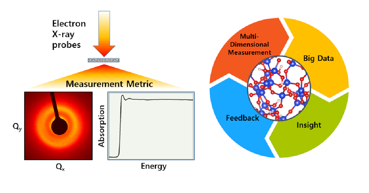
The development of next-generation materials in the fields of high-temperature superconductivity, battery, catalysis, and biomaterials has placed heavy emphasis on the functional properties of matter. At the most fundamental level, such properties are dictated by the spatial arrangements of atoms, molecules and their electronic structures. Accessing relevant information requires measurements be taken at a length scale that is considerably smaller than a billionth of a meter. However, even the most advanced visible light microscopes are unable to detect such atomic-level features due to the wavelength limitation, which is a thousand times larger than inter-atomic spacing.
X-ray and electron beams have been the primary means of probing the positions and configurations of atoms in various condensed matter systems ranging from simple solids to amorphous materials, such as liquids and glasses. Since their wavelengths are comparable to atomic size and their energies are suitable for accessing electronic binding energy, today's most advanced synchrotron sources and electron microscopes can be used to visualize atomic and electronic structures. Improved source coherence and detector technologies also offer unique opportunities for researchers to follow dynamical phenomena.
For this Special Issue, we are inviting submissions that exploring advanced measurement and analysis methods by using x-rays and electrons to study structural and electronic properties. Improving source brightness puts equal demands on light sources, optics, detectors, data processing, storage, and data analysis and modeling. More specifically, this issue aims to cover areas such as the structural analysis of crystalline and non-crystalline orders, measurement of electronic structure and performance of energy level analysis, advanced light sources, as well as detector and data acquisition methods. Opportunities in time-resolved measurements, artificial intelligence for data analysis, and other novel approaches remain open. We invite submissions in all these areas, as well as reviews of relevant fields.
Dr. Sooheyong Lee
Dr. Jihwan Kwon
Dr. Janghyun Jo
Guest Editors
Manuscript Submission Information
Manuscripts should be submitted online at www.mdpi.com by registering and logging in to this website. Once you are registered, click here to go to the submission form. Manuscripts can be submitted until the deadline. All submissions that pass pre-check are peer-reviewed. Accepted papers will be published continuously in the journal (as soon as accepted) and will be listed together on the special issue website. Research articles, review articles as well as short communications are invited. For planned papers, a title and short abstract (about 100 words) can be sent to the Editorial Office for announcement on this website.
Submitted manuscripts should not have been published previously, nor be under consideration for publication elsewhere (except conference proceedings papers). All manuscripts are thoroughly refereed through a single-blind peer-review process. A guide for authors and other relevant information for submission of manuscripts is available on the Instructions for Authors page. Materials is an international peer-reviewed open access semimonthly journal published by MDPI.
Please visit the Instructions for Authors page before submitting a manuscript. The Article Processing Charge (APC) for publication in this open access journal is 2600 CHF (Swiss Francs). Submitted papers should be well formatted and use good English. Authors may use MDPI's English editing service prior to publication or during author revisions.
Keywords
- transmission electron microscopy
- 4D STEM
- electron energy loss spectroscopy
- high-speed detection
- time-resolved X-ray diffraction
- time-resolved electron diffraction
- temporal correlation
- extended X-ray absorption fine structure
Benefits of Publishing in a Special Issue
- Ease of navigation: Grouping papers by topic helps scholars navigate broad scope journals more efficiently.
- Greater discoverability: Special Issues support the reach and impact of scientific research. Articles in Special Issues are more discoverable and cited more frequently.
- Expansion of research network: Special Issues facilitate connections among authors, fostering scientific collaborations.
- External promotion: Articles in Special Issues are often promoted through the journal's social media, increasing their visibility.
- e-Book format: Special Issues with more than 10 articles can be published as dedicated e-books, ensuring wide and rapid dissemination.
Further information on MDPI's Special Issue policies can be found here.