materials-logo

Journal Browser

Journal Browser

Current Research in Thin-Film Deposition: From Principles and Technologies to Film Properties and Applications

A special issue of Materials (ISSN 1996-1944). This special issue belongs to the section "Thin Films and Interfaces".

Deadline for manuscript submissions: 20 September 2024 | Viewed by 2243

Special Issue Editors


E-Mail Website
Guest Editor
Applied Physics and Semiconductor Spectroscopy, Brandenburg University of Technology Cottbus–Senftenberg, Konrad-Zuse-Strasse 1, D-03046 Cottbus, Germany
Interests: surface physics and chemistry; model heterogeneous catalysis; transition metal and rare-earth oxides; low-dimensional materials
Special Issues, Collections and Topics in MDPI journals

E-Mail Website
Guest Editor
Applied Physics and Semiconductor Spectroscopy, Brandenburg University of Technology Cottbus–Senftenberg, Konrad-Zuse-Strasse 1, D-03046 Cottbus, Germany
Interests: nanoscience; material characterization; thin films and nanothecnology; synchrotron facilities

Special Issue Information

Dear Colleagues,

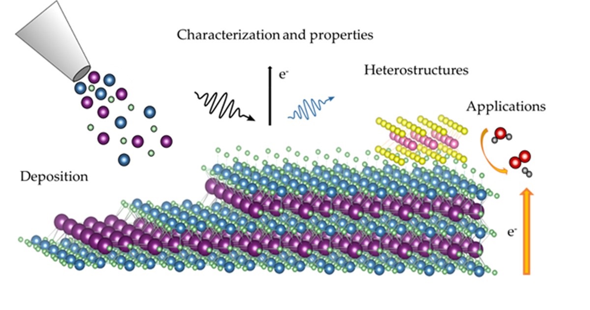
Thin films represent a mature, well-established field that bridges an almost unlimited range of potential applications, including functional coatings, optoelectronics, sensing, energy harvesting and storage, and heterogeneous catalysis. This variety is thanks to the unique properties of these films, which may substantially deviate from their bulk counterparts due to the small thickness, higher surface-to-volume ratio, strong interface interactions with other compounds in multiple device architectures, and internal microstructure.

Many of the abovementioned factors depend highly on the deposition technique; for example, the same compound can present rather distinct properties depending on its density, compactness, morphology, crystallinity, microstructure, or doping, all easily tunable by setting specific growth conditions for multiple physical or chemical deposition methods. Combined with the variety of multi-element compounds and all possible crystallographic structures, including the absence of the long-range order of amorphous and nanocrystalline films, the possibilities for multiple applications are countless, which explains why, after decades of intense work, the thin-film field remains a hot experimental and theoretical research topic both in terms of characterization and optimization.   

Furthermore, the appearance of 2D materials in recent years, together with the industrial requirements in terms of device miniaturization, has pushed the thin-film community towards new questions and challenges, driving the field into making thinner devices based on single layers or the synthesis of heterostructures by combining multiple 2D materials with more classical nanometric or micrometric thin-film architectures.

Considering this exciting framework, this Special Issue is seeking a comprehensive overview of the latest developments in thin-film deposition and synthesis, covering areas from first principles to deposition technologies, film properties including 2D-based materials, and applications. We invite you to submit an original manuscript, state-of-the-art review, communication, or topic discussion.

Prof. Dr. Jan Ingo Flege
Dr. Carlos Morales
Guest Editors

Manuscript Submission Information

Manuscripts should be submitted online at www.mdpi.com by registering and logging in to this website. Once you are registered, click here to go to the submission form. Manuscripts can be submitted until the deadline. All submissions that pass pre-check are peer-reviewed. Accepted papers will be published continuously in the journal (as soon as accepted) and will be listed together on the special issue website. Research articles, review articles as well as short communications are invited. For planned papers, a title and short abstract (about 100 words) can be sent to the Editorial Office for announcement on this website.

Submitted manuscripts should not have been published previously, nor be under consideration for publication elsewhere (except conference proceedings papers). All manuscripts are thoroughly refereed through a single-blind peer-review process. A guide for authors and other relevant information for submission of manuscripts is available on the Instructions for Authors page. Materials is an international peer-reviewed open access semimonthly journal published by MDPI.

Please visit the Instructions for Authors page before submitting a manuscript. The Article Processing Charge (APC) for publication in this open access journal is 2600 CHF (Swiss Francs). Submitted papers should be well formatted and use good English. Authors may use MDPI's English editing service prior to publication or during author revisions.

Keywords

  • thin-film deposition
  • thin-film properties
  • thin-film applications
  • first principles of thin films
  • 2D materials
  • heterostructures

Published Papers (3 papers)

Order results
Result details
Select all
Export citation of selected articles as:

Research

26 pages, 9005 KiB  
Article
Sol-Gel Multilayered Niobium (Vanadium)-Doped TiO2 for CO Sensing and Photocatalytic Degradation of Methylene Blue
by Simeon Simeonov, Anna Szekeres, Maria Covei, Hermine Stroescu, Madalina Nicolescu, Paul Chesler, Cristian Hornoiu and Mariuca Gartner
Materials 2024, 17(8), 1923; https://doi.org/10.3390/ma17081923 - 22 Apr 2024
Viewed by 431
Abstract
Multilayered TiO2 films doped either with Niobium or Vanadium (1.2 at. %) were deposited by the sol-gel dip coating method on c-Si and glass substrates. The films on glass substrates were tested for CO sensing and photocatalytic degradation of methylene blue. X-ray [...] Read more.
Multilayered TiO2 films doped either with Niobium or Vanadium (1.2 at. %) were deposited by the sol-gel dip coating method on c-Si and glass substrates. The films on glass substrates were tested for CO sensing and photocatalytic degradation of methylene blue. X-ray diffraction data analysis showed that all the TiO2:Nb(V) films were nanocrystalline in the anatase phase, with a uniform and compact microstructure and a homogeneous superficial structure of small grains with diameters in the range of 13–19 nm. For the electrical characterization, the TiO2:Nb(V) films were incorporated in Metal-Insulator-Semiconductor (MIS) structures. The specific resistivity is of the order of 104 Ωcm and its value decreases with increasing the electrical field, which testifies to the injection of electrons into these layers. From the analysis of the current–voltage curves taken at different temperature- and frequency—dependent capacitance–voltage and conductance–voltage characteristics, the density and parameters of deep levels in these TiO2 films are evaluated and the electron charge transport mechanism is established. It was shown that the current in these TiO2:Nb(V)-Si MIS structures is mainly carried out by inter-trap tunneling via deep levels energetically distributed in the TiO2 bandgap. Testing these sol-gel TiO2:Nb(V) layers for gas sensing and photocatalytic capabilities proved that they could serve such purposes. In particular, the results of the V-doped sol-gel TiO2 film confirm its CO detection capability, which is rarely reported in the literature. For the photodegradation of methylene blue, the Nb-doped TiO2 samples were superior, with nearly double the photocatalytic efficiency of undoped TiO2. Full article
Show Figures

Figure 1

13 pages, 5158 KiB  
Article
Conductive Nanosheets Fabricated from Au Nanoparticles on Aqueous Metal Solutions under UV Irradiation
by Maho Tagawa, Hiroto Kaneki and Takeshi Kawai
Materials 2024, 17(4), 842; https://doi.org/10.3390/ma17040842 - 9 Feb 2024
Viewed by 670
Abstract
Highly transparent, conductive nanosheets are extremely attractive for advanced opto-electronic applications. Previously, we have demonstrated that transparent, conductive Au nanosheets can be prepared by UV irradiation of Au nanoparticle (AuNP) monolayers spread on water, which serves as the subphase. However, thick Au nanosheets [...] Read more.
Highly transparent, conductive nanosheets are extremely attractive for advanced opto-electronic applications. Previously, we have demonstrated that transparent, conductive Au nanosheets can be prepared by UV irradiation of Au nanoparticle (AuNP) monolayers spread on water, which serves as the subphase. However, thick Au nanosheets cannot be fabricated because the method is not applicable to large Au NPs. Further, in order to fabricate nanosheets with different thicknesses and compositions, it is necessary to prepare the appropriate NPs. A strategy is needed to produce nanosheets with different thicknesses and compositions from a single type of metal NP monolayer. In this study, we show that this UV irradiation technique can easily be extended as a nanosheet modification method by using subphases containing metal ions. UV irradiation of 4.7 nm AuNP monolayers on 480 µM HAuCl4 solution increased the thickness of Au nanosheets from 3.5 nm to 36.5 nm, which improved conductivity, but reduced transparency. On the other hand, the use of aqueous AgNO3 and CH3COOAg solutions yielded Au-Ag hybrid nanosheets; however, their morphologies depended on the electrolytes used. In Au-Ag nanosheets prepared on aqueous 500 µM AgNO3, Au and Ag metals are homogeneously distributed throughout the nanosheet. On the other hand, in Au-Ag nanosheets prepared on aqueous 500 µM CH3COOAg, AuNPs still remained and these AuNPs were covered with a Ag nanosheet. Further, these Au-Ag hybrid nanosheets had high conductivity without reduced transparency. Therefore, this UV irradiation method, modified by adding metal ions, is quite effective at improving and diversifying properties of Au nanosheets. Full article
Show Figures

Figure 1

23 pages, 15684 KiB  
Article
Effects of Direct and Pulse Plating on the Co-Deposition of Sn–Ni/TiO2 Composite Coatings
by Eleni Rosolymou, Antonis Karantonis and Evangelia A. Pavlatou
Materials 2024, 17(2), 392; https://doi.org/10.3390/ma17020392 - 12 Jan 2024
Viewed by 778
Abstract
Sn–Ni alloy matrix coatings co-deposited with TiO2 nanoparticles (Evonik P25) were produced utilizing direct (DC) and pulse electrodeposition (PC) from a tin–nickel chloride-fluoride electrolyte with a loading of TiO2 nanoparticles equal to 20 g/L. The structural and morphological characteristics of the [...] Read more.
Sn–Ni alloy matrix coatings co-deposited with TiO2 nanoparticles (Evonik P25) were produced utilizing direct (DC) and pulse electrodeposition (PC) from a tin–nickel chloride-fluoride electrolyte with a loading of TiO2 nanoparticles equal to 20 g/L. The structural and morphological characteristics of the resultant composite coatings were correlated with the compositional modifications that occurred within the alloy matrix and expressed via a) TiO2 co-deposition rate and b) composition of the matrix; this was due to the application of different current types (DC or PC electrodeposition), and different current density values. The results demonstrated that under DC electrodeposition, the current density exhibited a more significant impact on the composition of the alloy matrix than on the incorporation rate of the TiO2 nanoparticles. Additionally, PC electrodeposition favored the incorporation rate of TiO2 nanoparticles only when applying a low peak current density (Jp = 1 Adm−2). All of the composite coatings exhibited the characteristic cauliflower-like structure, and were characterized as nano-crystalline. The composites’ surface roughness demonstrated a significant influence from the TiO2 incorporation rate. However, in terms of microhardness, higher co-deposition rates of embedded TiO2 nanoparticles within the alloy matrix were associated with decreased microhardness values. The best wear performance was achieved for the composite produced utilizing DC electrodeposition at J = 1 Adm−2, which also demonstrated the best photocatalytic behavior under UV irradiation. The corrosion study of the composite coatings revealed that they exhibit passivation, even at elevated anodic potentials. Full article
Show Figures

Figure 1

Back to TopTop