A New Bridgeless High Step-up Voltage Gain PFC Converter with Reduced Conduction Losses and Low Voltage Stress


1
State Key Laboratory of Electrical Insulation and Power Equipment, School of Electrical Engineering, Xi’an Jiaotong University, Xi’an 710049, China
2
School of Electrical, Electronic and Computer Engineering, The University of Western Australia, Crawley W.A. 6009, Australia
*
Author to whom correspondence should be addressed.
Energies 2018, 11(10), 2640; https://doi.org/10.3390/en11102640
Submission received: 24 August 2018
/
Revised: 25 September 2018
/
Accepted: 1 October 2018
/
Published: 2 October 2018
(This article belongs to the Special Issue Control and Nonlinear Dynamics on Energy Conversion Systems)
Abstract
:Bridgeless power factor correction (PFC) converters have a reduced number of semiconductors in the current flowing path, contributing to low conduction losses. In this paper, a new bridgeless high step-up voltage gain PFC converter is proposed, analyzed and validated for high voltage applications. Compared to its conventional counterpart, the input rectifier bridge in the proposed bridgeless PFC converter is completely eliminated. As a result, its conduction losses are reduced. Also, the current flowing through the power switches in the proposed bridgeless PFC converter is only half of the current flowing through the rectifier diodes in its conventional counterpart, therefore, the conduction losses can be further improved. Moreover, in the proposed bridgeless PFC converter, not only the voltage stress of power switches is lower than the output voltage, but the voltage stress of the output diodes is lower than the conventional counterpart. In addition, this proposed bridgeless PFC converter features a simple circuit structure and high PFC performance. Finally, the proposed bridgeless PFC converter is analyzed and designed in the discontinuous conduction mode (DCM). The simulation results are presented to verify the effectiveness of the proposed bridgeless PFC converter.
1. Introduction
In the past decades, AC-DC converters have been widely used in numerous power electronic equipment supplied by the power grid in order to obtain the DC voltage. For the passive AC-DC rectifier, the input current harmonics are large, which is very harmful for the power grid and other power electronic equipment. In order to alleviate the input current harmonics and satisfy the rigorous input current harmonic standards, for instance, the IEC 61000-3-2 criterion, the active power factor correction (PFC) converter has become a popular and effective method to shape the input current waveform and achieve the near unity power factor (PF) in the power supplies. For single-phase power supplies, the boost topology is the most popular option as the PFC pre-regulator, by reason of its simple circuit structure and high PFC performance [1,2,3]. Unfortunately, the boost topology cannot achieve a very high voltage gain in practical applications, because the extremely high duty cycle is unpractical. Therefore, in some high voltage applications, for example, X-ray medical/industry equipment, HVDC system insulator testing, electrostatic precipitators and high voltage battery charger, the boost PFC converter is a poor candidate, especially for the universal line [4,5].
For outputting high voltage, many conventional high step-up voltage gain PFC converters have been studied in the past decade [6,7,8,9,10,11,12,13,14,15,16]. Based on the Cockcroft–Walton (CW) structure, some high step-up voltage gain PFC converters were proposed in [6,7,8,9,10]. In [6], a three-stage CW PFC converter was proposed. This converter can achieve a high output voltage and a high PFC performance. In [7], a transformerless hybrid boost and CW PFC converter was presented. By adding the CW voltage multiplier (VM) stages, high output voltage and high power factor are obtained. A single-phase single-stage high step-up matrix PFC converter using CW-VM was proposed in [8]. By combining a four bidirectional-switch matrix converter and the CW-VM, a high step-up voltage gain is achieved. Based on [6], a more comprehensive analysis and validation were presented in [9]. Based on [9], an improved high step-up voltage gain PFC converter with soft-switching characteristic was introduced in [10]. Besides the CW structure, some efforts focused on the switched-capacitor PFC topology to produce the high output voltage [11,12,13]. In [11], a family of high-voltage gain hybrid switched-capacitor PFC converters were proposed and validated, which can achieve a high output voltage and good PFC performance. A high voltage gain PFC converter based on a hybrid boost DC-DC converter was presented in [12]. By integrating boost topology and the switched-capacitor voltage doubler, a high output voltage and nearly unity PF are produced. In [13], a hybrid single ended primary inductor converter (SEPIC) PFC converter using switched-capacitor voltage doubler was proposed, which also owns a high voltage gain and a good PFC performance. Other new PFC converters can also achieve a high voltage gain [14,15,16]. In [14], a single-stage boost PFC converter with zero current switching (ZCS) characteristic was proposed and studied, which has a high voltage gain. In [15], a modified SEPIC PFC converter with a high voltage gain was proposed. A family of ZCS isolated high voltage gain PFC converters were proposed in [16]. Also, many high step-up voltage gain DC-DC converters have been studied in [17,18,19,20,21,22,23,24]. These DC-DC topologies can also be applied as the PFC converters for the high voltage applications. However, all the PFC converters, as mentioned above [6,7,8,9,10,11,12,13,14,15,16,17,18,19,20,21,22,23,24], are the conventional PFC type. The rectifier bridge is necessary for them, and their topology structures are more complex.
Compared to the conventional PFC converters, the bridgeless PFC converters possess the merits of low conduction losses and higher efficiency. That is because the input rectifier diodes of the bridgeless PFC converters are reduced, leading to a less number of semiconductors in the current-flowing path [2]. In order to improve efficiency, some bridgeless PFC converters with high output voltage are proposed in [25,26,27]. In [25], a bridgeless Cuk PFC converter was proposed for high voltage battery charger. In [26], a bridgeless modified SEPIC PFC converter was proposed with extended voltage gain. Two bridgeless hybrid boost PFC converters using the switched-capacitor structure were presented in [27]. All these bridgeless PFC converters can be applied for the high voltage applications, and their efficiency are improved compared to their conventional counterparts.
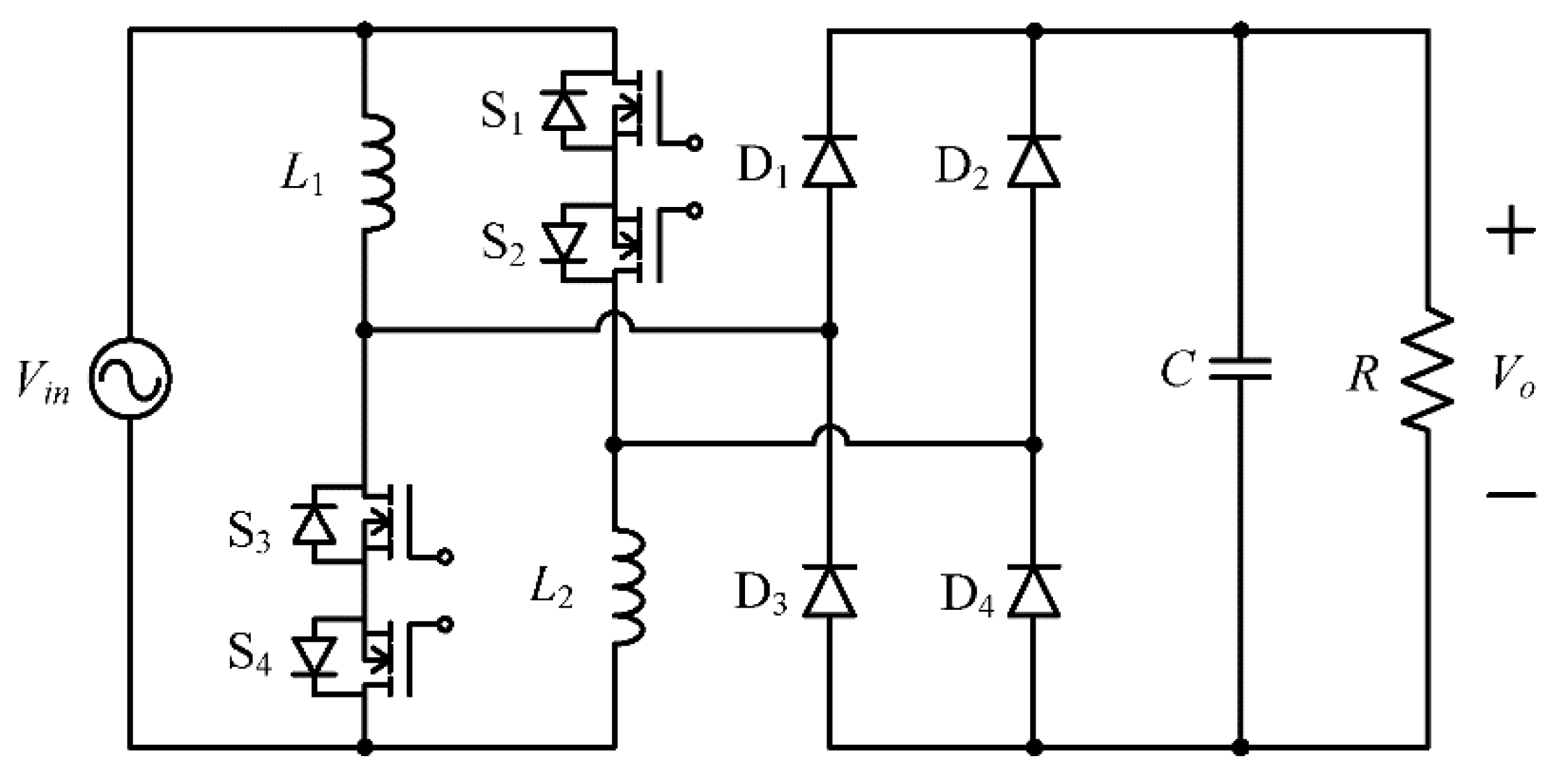
Based on the conventional high step-up voltage gain PFC converter shown in Figure 1, which was first proposed in [18] as the DC-DC converter, a new bridgeless high step-up voltage gain PFC converter with improved efficiency shown in Figure 2 is proposed for high voltage applications. By reducing the number of semiconductors in the current-flowing path and reducing the current stress of semiconductors, the proposed bridgeless PFC converter can achieve a reduced conduction losses and a higher efficiency compared to its conventional counterpart. Besides, the proposed bridgeless PFC converter owns a lower voltage stress of output diodes than the conventional one. The high PF and low total harmonic distortion (THD) are also obtained in the proposed bridgeless PFC converter. In addition, the proposed bridgeless PFC converter features a very simple circuit structure, contributing to cost and power density. The discontinuous conduction mode (DCM) is utilized with the merits of zero current turned on in the power switches, zero current turned off in the diodes, nature current-sharping ability and a simple control method. As a result, the proposed bridgeless PFC converter is more suitable for the high voltage applications than its conventional counterpart.
2. Operation Principle
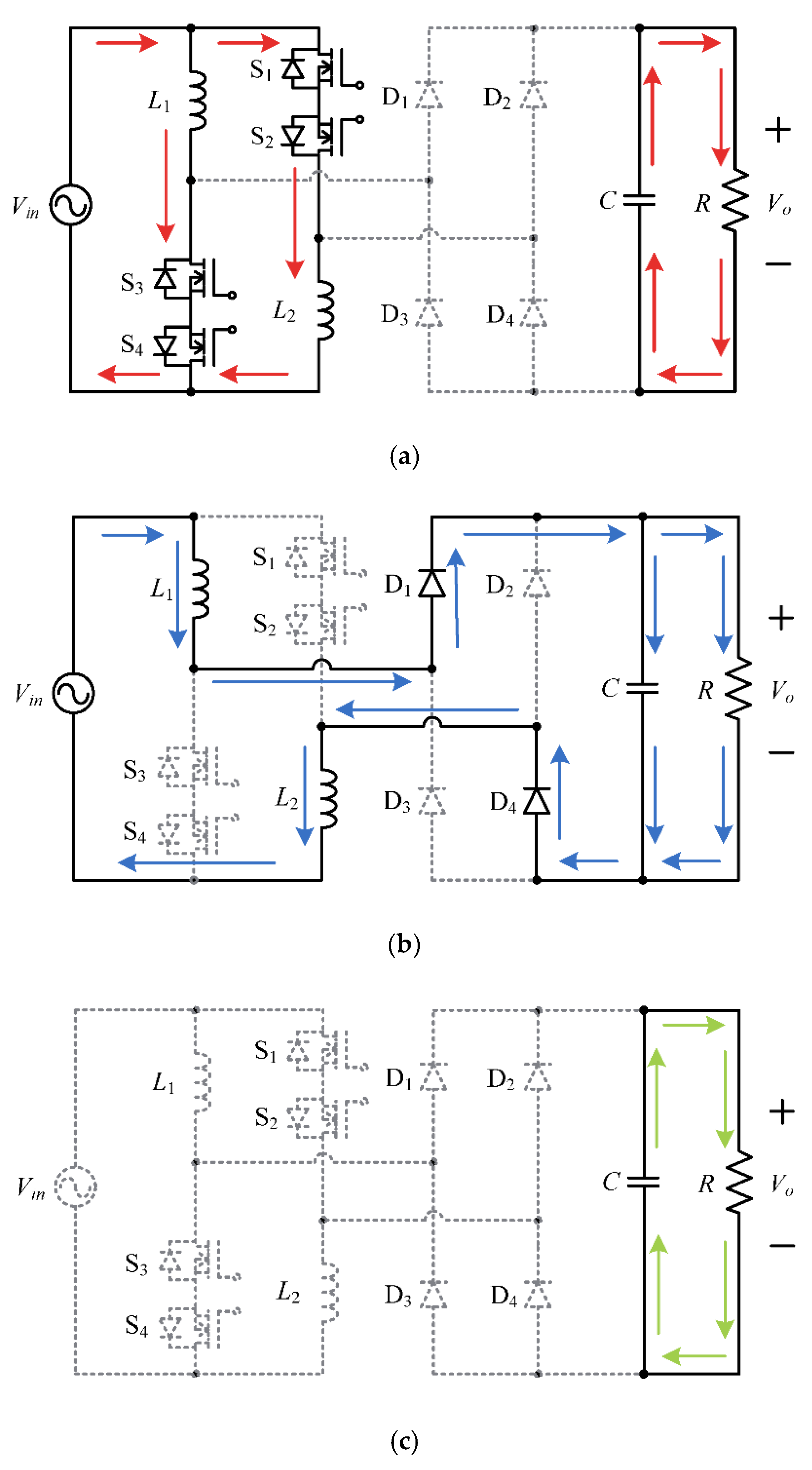
This proposed bridgeless high step-up voltage gain PFC converter uses two bidirectional switches in series with two same level inductors. Each bidirectional switch is constructed by two anti-series power switches. It should be noted that the two power switches in one bidirectional switch have the common source terminal, which can simplify the drive circuit. Simultaneously, an output bridge including D1, D2, D3 and D4 which are fast-recovery diodes is used to obtain a high DC output voltage in the proposed bridgeless PFC converter, while only D5 is the fast-recovery diode in its conventional counterpart. The proposed bridgeless PFC converter is designed to operate in DCM. Thereby, it has three operation modes during one switching period. The detailed operation modes of one switching period in the positive line cycle are presented in Figure 3. Since the proposed bridgeless PFC converter is symmetrical, the operation modes in negative line cycle are similar to the modes in positive line cycle. Its key time-domain waveforms are exhibited in Figure 4.
Mode I shown in Figure 3a: when the power switches S1 and S3 are turned on, the input sinusoidal source vin charges the two inductors L1 and L2, simultaneously, through the power switches S2 and S4. The output bulk capacitor maintains the output voltage vo. In each branch of the proposed bridgeless PFC converter, only two semiconductors consisting by two power switches are active, while three semiconductors are active in one branch of the conventional counterpart. In this mode, the inductor currents satisfy:
Mode II shown in Figure 3b: when all the power switches are turned off, the input source and the two inductors releases energies to the load. Only two output fast-recovery diodes conduct in this mode, while three semiconductors including two slow-recovery diodes and one fast-recovery diode conduct in the corresponding conventional counterpart. In this mode, the inductor currents satisfy:
Mode III shown in Figure 3c: all the semiconductors are in the off state. The inductor currents are zero. The output bulk capacitor C maintains the output voltage.
Figure 4 presents the key waveforms of duty cycle D, inductor current iL1, iL2, input current iin, and the voltage vS1, vS3, vD1, vD4 across the semiconductors in the positive line cycle. From this figure, the inductor current iL1, iL2 are equal to each other. When the power switches are turned on, the inductor current are half of the input current iin. When the power switches are turned off, the inductor current are same with the input current. The maximum voltage across the power switches and the output diodes are (vin + vo)/2 in the positive line cycle. It should be noted that the duty cycle D equals to (t2 − t1)/TS, where TS is the switching period.
3. Theoretical Analysis
The detailed theoretical analysis and designed consideration in DCM are presented in this subsection. First of all, some ideal assumptions are provided to simplify the analysis. Notably, the theoretical analysis is made in one positive line cycle. These assumptions are shown as follows:
- The switching frequency fs is much higher than the line frequency. Thus, the input voltage is constant during one switching period.
- The capacitance of the bulk capacitor is large enough. Thereby, the output voltage is ideal constant.
- All the components are ideal without losses.
- The input voltage is ideally sinusoidal.
3.1. The Voltage Conversion Ratio M
Appling the voltage-second balance principle to the inductor L1, the voltage conversion ratio M is derived as follows:
where vm is the amplitude of the sinusoidal input voltage vin, θ is the angle of the input voltage vin, and Dx is equal to (t3 − t2)/TS.
Based on (3), the relationship between the duty cycle D and Dx can be expressed as:
In addition, the peak inductor current iL1-peak in one switching period is:
Due to the power balance between input power and output power, we can get:
Substituting (4) and (5) into (6), the relationship of the voltage conversion ratio M and duty cycle D is derived as follows:
where the dimensionless conduction parameter K is:
and the parameter β is
The relationship of the voltage conversion ratio M and duty cycle D is presented in Figure 5. From this figure, one can see that the voltage conversion ratio M increases with the lower parameter K. Compared to the conventional boost PFC converter, the voltage conversion ratio M of the proposed bridgeless PFC converter is much higher. Therefore, the proposed bridgeless PFC converter is more suitable for the high voltage applications.
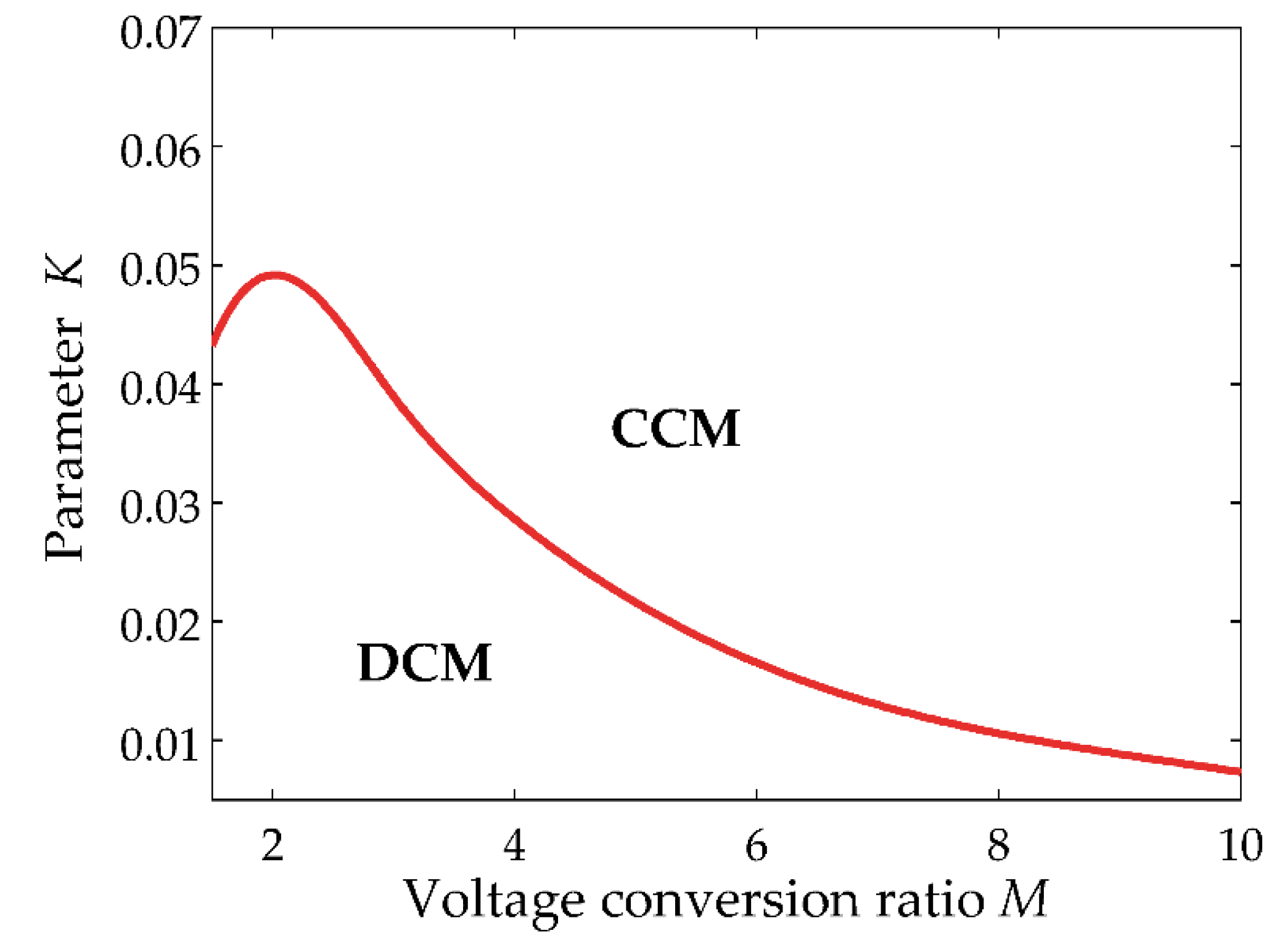
3.2. The Operation Conditon for DCM
In order to operate in DCM, the operation condition must satisfy as follows:
Substituting (3) and (7) into (10), the operation condition for DCM is derived as:
The proposed bridgeless PFC converter is designed to operate in DCM totally. Therefore, the inductor currents should be discontinuous at the peak point in the line cycle. Thus, the simplified operation condition for DCM is:
Figure 6 draws the operation boundary between the DCM and the continuous conduction mode (CCM). From this figure, the operation boundary is higher at the low voltage conversion ratio. However, for the universal line, the voltage conversion ratio is different under different input voltage. Hence, the key parameter K must be designed at the lowest input voltage.
3.3. The Voltage Stress and Current Stress
The voltage stress of semiconductors in the proposed bridgeless PFC converter and in its conventional bridge counterpart are shown in Table 1. From this table, the voltage stress of power switch in the proposed bridgeless PFC converter is same with its conventional bridge converter, and it is lower than the output voltage. The voltage stress of fast-recovery diode in the proposed bridgeless PFC converter is lower than that in the conventional bridge converter. Therefore, the lower rated diode can be used in the proposed bridgeless PFC converter. It is beneficial to improve cost and losses. In addition, no slow-recovery diode is used in the proposed bridgeless PFC converter, while four slow-recovery diodes as the input bridge are used in its conventional bridge counterpart, and their voltage stress is vm.
The root-mean-square (RMS) current iS1-rms of power switch in one switching period is shown as follows:
The averaged current iD1-avg of output diode in one switching period is derived as follows:
3.4. The Conduction Losses
In this subsection, the conduction losses of semiconductors are calculated. The detail derivations in one positive line cycle are exhibited as follows:
where Ron is the conduction resistance of the power switch and VF is the forward voltage of diodes.
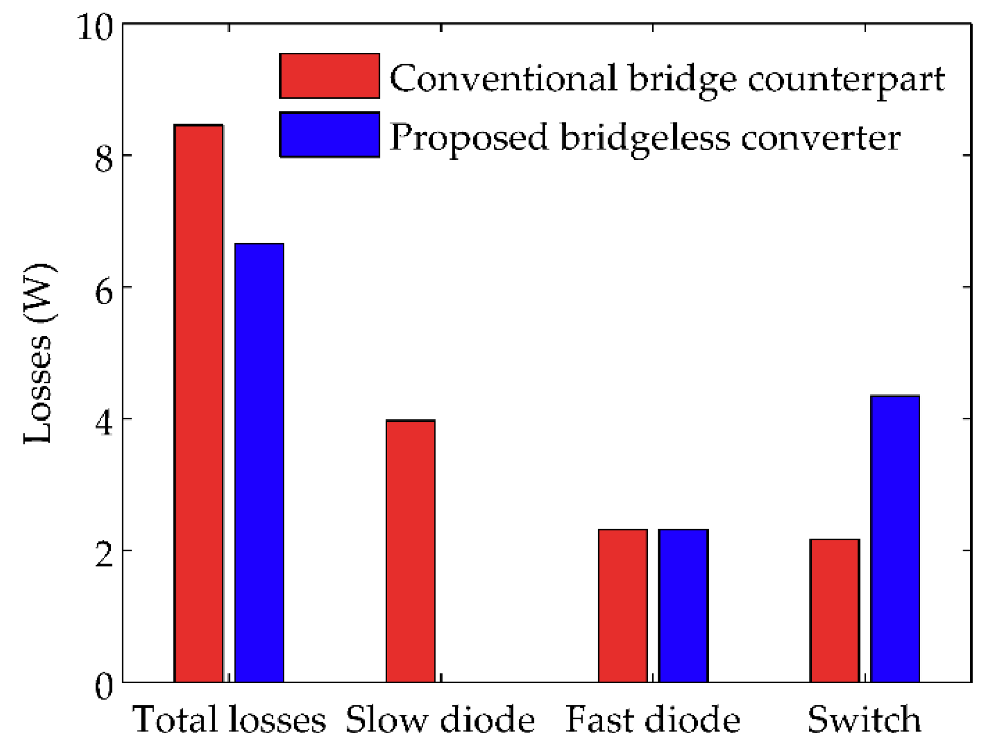
Under the operation condition vin = 220 Vrms/50 Hz, vo = 800 V, fs = 30 kHz and Po = 500 W, the conduction losses of semiconductors are calculated. It should be noted that the parameters Ron and VF are chosen from the datasheet of the selected components. The conduction losses of semiconductors of the proposed bridgeless PFC converter and its conventional counterpart are presented in Figure 7. From this figure, it can be found that the total conduction losses of semiconductors in the proposed bridgeless PFC converter is much lower than its conventional bridge counterpart. The conduction losses of power switches in the proposed bridgeless PFC converter are higher, while it has no conduction losses of input rectifier diodes.
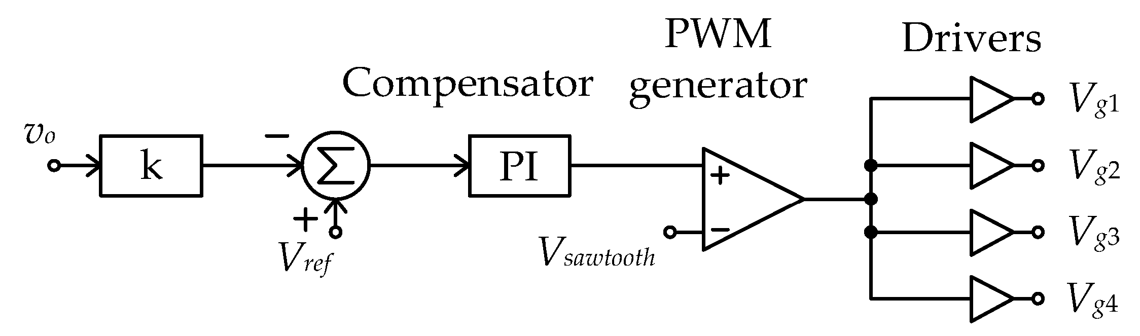
3.5. The Control Principle
This proposed bridgeless PFC converter is designed in DCM. The DCM possesses the merit of a naturally current-sharping ability, which contributes to a simple control method. Thereby, the voltage control loop is applied in order to obtain the constant DC output voltage. The control principle is displayed in Figure 8. From this figure, the controller mainly contains one compensator, one PWM generator and four drivers. It should be noted that the four power switches in the proposed bridgeless PFC converter can be driven by one same control signal, which simplifies the controller, significantly. Notably, the signal Vg1, Vg2, Vg3 and Vg4 drive the power switches S1, S2, S3 and S4, respectively.
4. Simulation Results
The effectiveness of the proposed bridgeless PFC converter is validated in the SIMetrix/SIMPLIS (version 8.00, company SIMetrix Technologies Ltd., Thatcham, UK) environment. The simulation program with integrated circuit emphasis (SPICE) models of practical components are employed in this simulation. The key operation parameters of the proposed bridgeless PFC converter is vin = universal line 95–265 Vrms, vo = 800 V, fs = 30 kHz and Po = 500 W. The selected components are shown in Table 2. Considering the voltage stress, current stress and safety margin, the SPP17N80C3 (company Infineon, GER) with Ron = 0.29 Ω and VDS = 800 V is chosen as the power switches. The MUR490 (company On Semiconductor, Phoenix, AZ, USA) with VF = 1.85 V and VD = 900 V is chosen as the fast-recovery diodes in the proposed bridgeless PFC converter. Since the voltage stress of the fast-recovery diode in the conventional bridge counterpart is up to around 1200 V, which is much larger than the voltage stress 800 V of the fast-recovery diode in the proposed bridgeless PFC converter, we have to choose two series MUR490 as the fast-recovery diode in the conventional bridge counterpart. In the conventional bridge converter, 8EWS08 (company International Rectifier, El Segundo, CA, USA) with VF = 1 V is used as the input rectifier diodes.
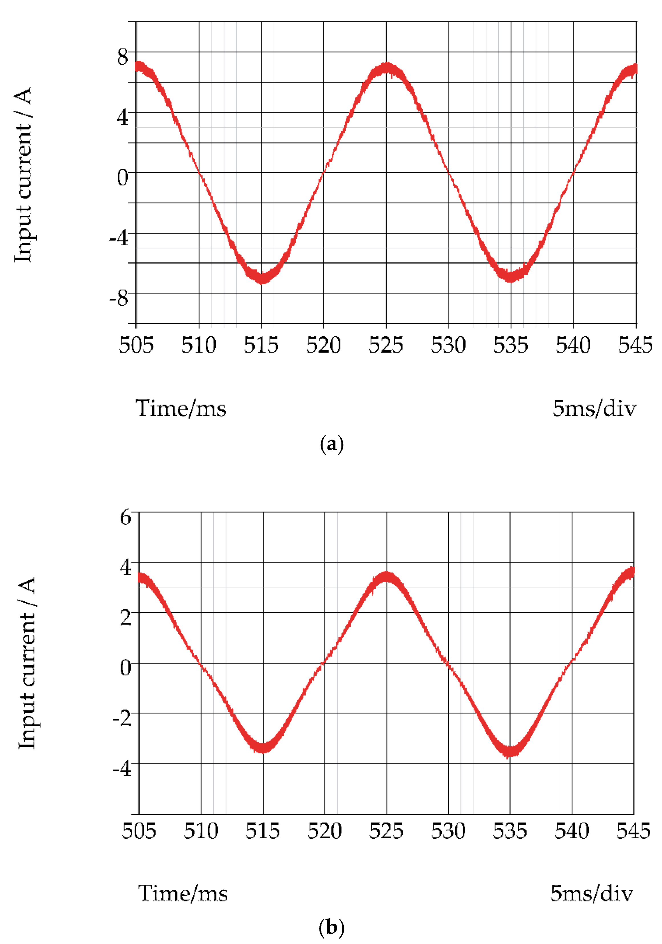
The input current after the input LC filter at the typical input line is displayed in Figure 9. From this figure, the input current is shaped to be almost sinusoidal at the typical low line 110 Vrms and the typical high line 220 Vrms. Thereby, it is validated that the proposed bridgeless PFC converter owns a good current-shaping ability. Figure 10 presents the key time-domain waveforms of the proposed bridgeless PFC converter. It can be figure out that the simulated waveforms are in agreement with the theoretical analysis. The key waveforms also validate that the proposed bridgeless PFC converter operates in DCM.
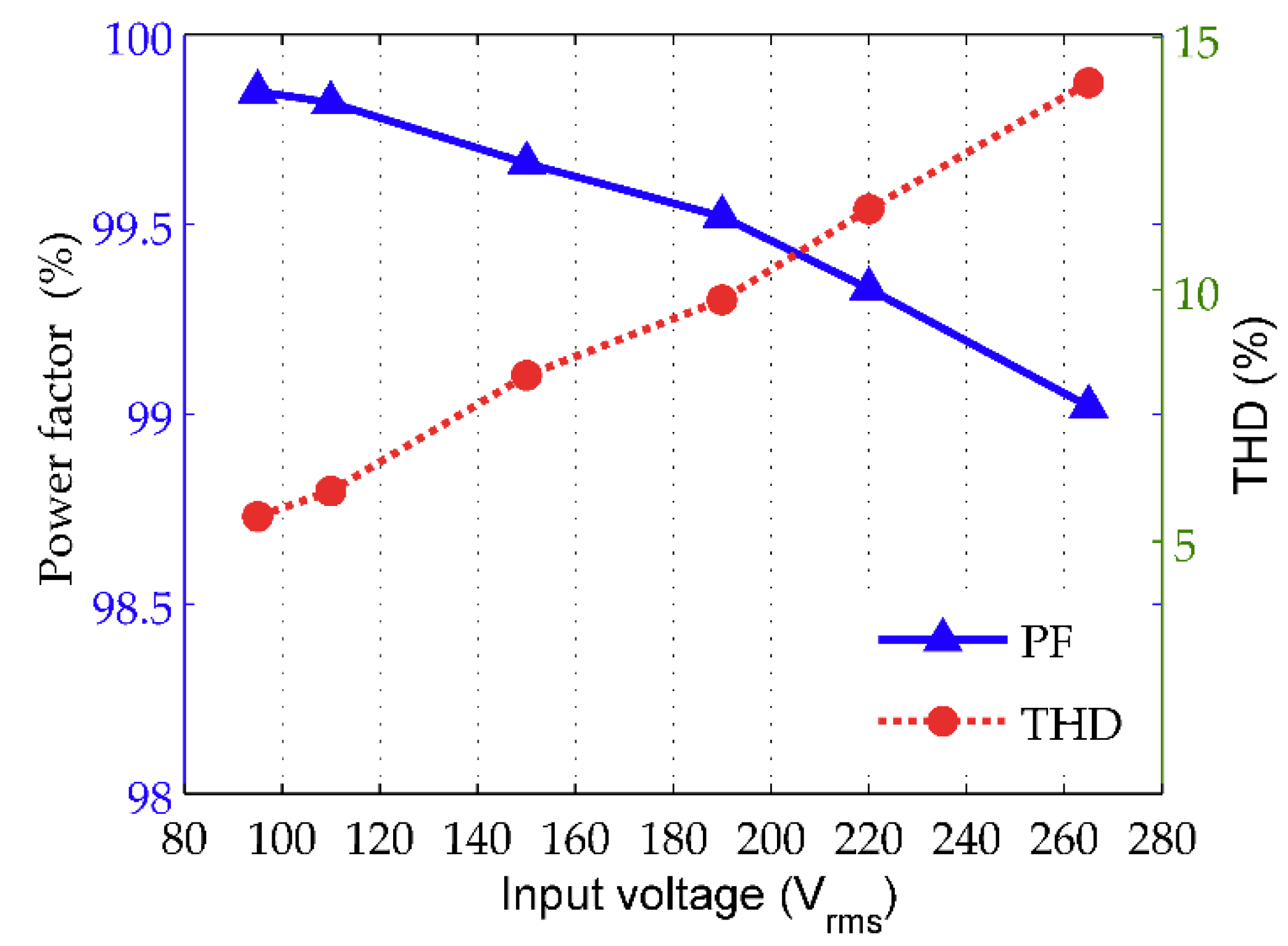
Figure 11 presents the simulated PF and THD under the universal line. From this figure, one can see that nearly unity PF is achieved and the THD is low under the universal line. The high PF and low THD validate that the proposed bridgeless PFC converter owns a good PFC performance.
The simulated efficiency of the proposed bridgeless PFC converter and its conventional bridge counterpart under the universal line is shown in Figure 12. From this figure, it is clear that the efficiency of the proposed bridgeless PFC converter is higher than its conventional bridge counterpart, due to the reduced semiconductors and the reduced current. Also, the efficiency of other state of the art high step-up voltage gain converter in [12] is simulated. Under the same operation parameters and components, the efficiency of the converter in [12] is 97.42% at the typical line Vin = 220 Vrms, while the efficiency of the proposed bridgeless PFC converter can reach up to 98.78% at the typical line Vin = 220 Vrms. Therefore, the proposed bridgeless PFC converter is more suitable for the practical application.
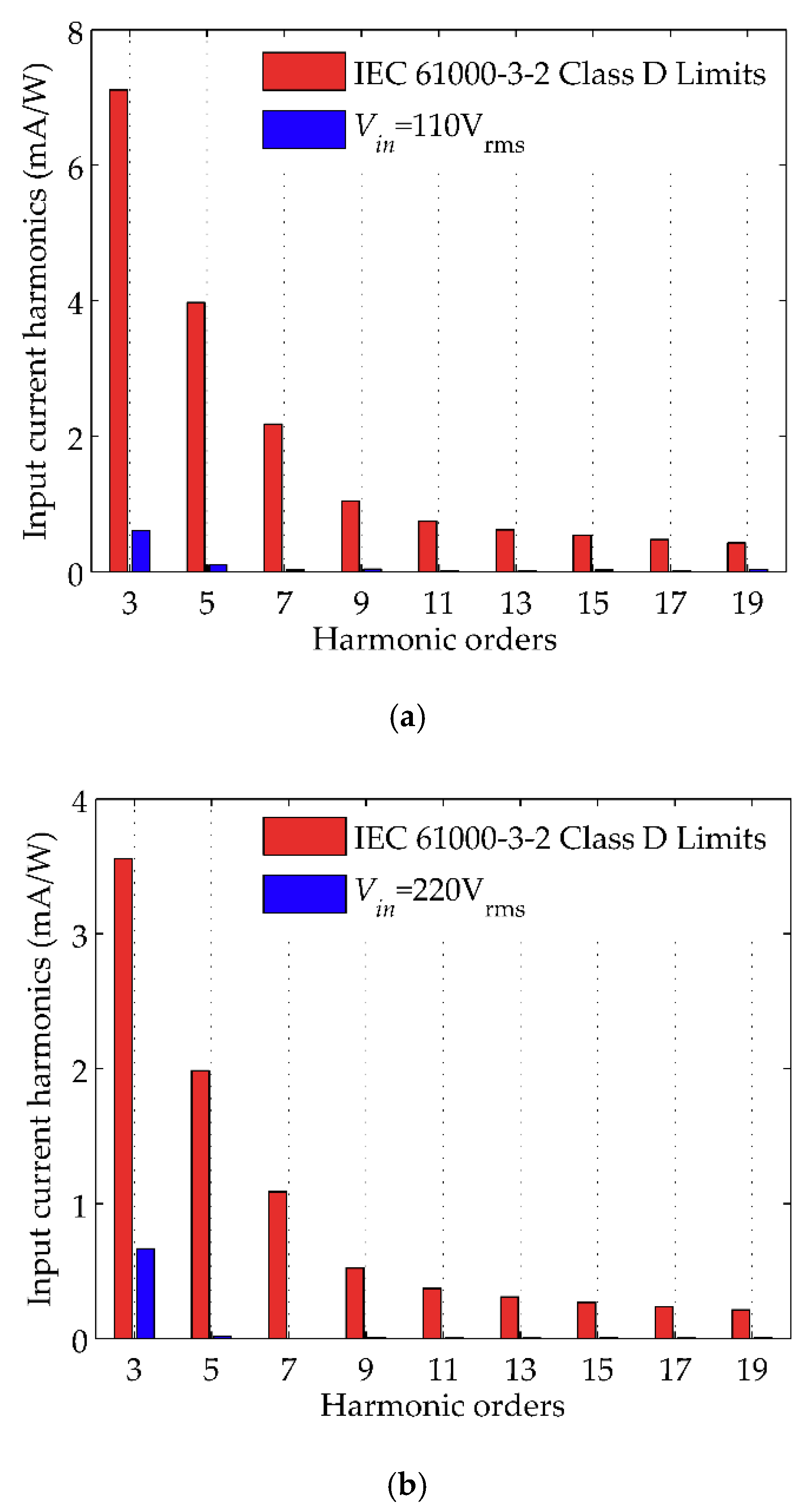
Figure 13 displays the simulated input current harmonics compared with the IEC 61000-3-2 class D limits. From this figure, the input current harmonics of the proposed bridgeless PFC converter are much lower than the IEC 61000-3-2 class D limits under both the typical low line and high line. Namely, the proposed bridgeless PFC converter can easily satisfy the international harmonic standards, which is very beneficial to practical application.
5. Conclusions
A new bridgeless high step-up voltage gain PFC converter with low conduction losses and low voltage stresses for high voltage applications is proposed, analyzed and verified in this paper. The theoretical analysis and design consideration in DCM are presented. The simulated results validate that the proposed bridgeless PFC converter has a higher efficiency than its conventional bridge counterpart. Moreover, the proposed bridgeless PFC converter can achieve a very high PF and low THD, and it can easily satisfy the IEC 61000-3-2 class D limits, thereby, the proposed bridgeless PFC converter is a competitive option for the high voltage applications.
Author Contributions
X.L. conceived, validated and wrote the manuscript. F.W. and H.H.C.I. participated in the research plan development and revised the manuscript. All authors contributed to the manuscript.
Funding
This work was supported in part by the National Natural Science Foundation of China under Grant 51377124 and Grant 51521065, in part by the New Star of Youth Science and Technology of Shaanxi Province under Grant 2016KJXX-40, and in part by the China Scholarship Council under Grant 201706285022.
Conflicts of Interest
The authors declare no conflict of interest.
References
- Salmon, J.C. Circuit topologies for single-phase voltage-doubler boost rectifiers. IEEE Trans. Power Electron. 1993, 8, 521–529. [Google Scholar] [CrossRef]
- Huber, L.; Jang, Y.; Jovanović, M.M. Performance evaluation of bridgeless PFC boost rectifiers. IEEE Trans. Power Electron. 2008, 23, 1381–1390. [Google Scholar] [CrossRef]
- Muhammad, K.S.B.; Lu, D.D. ZCS bridgeless boost PFC rectifier using only two active switches. IEEE Trans. Ind. Electron. 2015, 62, 2795–2806. [Google Scholar] [CrossRef]
- Bellar, M.D.; Watanabe, E.H.; Mesquita, A.C. Analysis of the dynamic and steady-state performance of Cockcroft-Walton cascade rectifiers. IEEE Trans. Power Electron. 1992, 7, 526–534. [Google Scholar] [CrossRef]
- Momayyezan, M.; Hredzak, B.; Agelidis, V.G. Integrated reconfigurable converter topology for high-voltage battery systems. IEEE Trans. Power Electron. 2016, 31, 1968–1979. [Google Scholar] [CrossRef]
- Young, C.M.; Chen, M.H. A novel single-phase AC to high voltage DC converter based on Cockcroft-Walton cascade rectifier. In Proceedings of the IEEE 2009 International Conference on Power Electronics and Drive Systems, Taipei, Taiwan, 2–5 November 2009; pp. 822–826. [Google Scholar]
- Young, C.M.; Chen, M.H.; Chen, H.L.; Chao, J.Y.; Ko, C.C. Transformerless single-stage high step-up AC-DC converter based on symmetrical Cockcroft-Walton voltage multiplier with PFC. In Proceedings of the IEEE Ninth International Conference on Power Electronics and Drive Systems, Singapore, 5–8 December 2011; pp. 191–196. [Google Scholar]
- Young, C.M.; Chen, M.H.; Yeh, S.H.; Yuo, K.H. A single-phase single-stage high step-up AC-DC matrix converter based on Cockcroft-Walton voltage multiplier with PFC. IEEE Trans. Power Electron. 2012, 27, 4894–4905. [Google Scholar] [CrossRef]
- Young, C.M.; Chen, M.H.; Ko, C.C. High power factor transformerless single-stage single-phase ac to high-voltage dc converter with voltage multiplier. IET Power Electron. 2012, 5, 149–157. [Google Scholar] [CrossRef]
- Young, C.M.; Wu, S.F.; Chen, M.H.; Chen, S.J. Single-phase AC to high-voltage DC converter with soft-switching and diode-capacitor voltage multiplier. IET Power Electron. 2014, 7, 1704–1713. [Google Scholar] [CrossRef]
- Cortez, D.F.; Barbi, I. A family of high-voltage gain single-phase hybrid switched-capacitor PFC rectifiers. IEEE Trans. Power Electron. 2015, 30, 4189–4198. [Google Scholar] [CrossRef]
- Cortez, D.F.; Maccarini, M.C.; Mussa, S.A.; Barbi, I. High static gain single-phase PFC based on a hybrid boost converter. Int. J. Electron. 2017, 104, 821–839. [Google Scholar] [CrossRef]
- Costa, P.J.S.; Font, C.H.I.; Lazzarin, T.B. Single-phase hybrid switched-capacitor voltage-doubler SEPIC PFC rectifiers. IEEE Trans. Power Electron. 2018, 33, 5118–5130. [Google Scholar] [CrossRef]
- Chen, J.F.; Chen, R.Y.; Liang, T.J. Study and implementation of a single-stage current-fed boost PFC converter with ZCS for high voltage applications. IEEE Trans. Power Electron. 2008, 23, 379–386. [Google Scholar] [CrossRef]
- Melo, P.F.D.; Gules, R.; Romaneli, E.F.R.; Annunziato, R.C. A modified SEPIC converter for high-power-factor rectifier and universal input voltage applications. IEEE Trans. Power Electron. 2010, 25, 310–321. [Google Scholar] [CrossRef]
- Li, C.; Xu, D. Family of enhanced ZCS single-stage single-phase isolated AC-DC converter for high-power high-voltage DC supply. IEEE Trans. Ind. Electron. 2017, 64, 3629–3639. [Google Scholar] [CrossRef]
- Wai, R.J.; Lin, C.Y.; Duan, R.Y.; Chang, Y.R. High efficiency DC-DC converter with high voltage gain and reduced switch stress. IEEE Trans. Ind. Electron. 2007, 54, 354–364. [Google Scholar] [CrossRef]
- Yang, L.S.; Liang, T.J.; Chen, J.F. Transformerless DC-DC converters with high step-up voltage gain. IEEE Trans. Ind. Electron. 2009, 56, 3144–3152. [Google Scholar] [CrossRef]
- Qian, W.; Cao, D.; Cintron-Rivera, J.G.; Gebben, M.; Wey, D.; Peng, F.Z. A swithed-capacitor DC-DC converter with high voltage gain and reduced component rating and count. IEEE Trans. Ind. Appl. 2012, 48, 1397–1406. [Google Scholar] [CrossRef]
- Tofoli, F.L.; Oliveira, D.S.; Torrico-Bascope, R.P.; Alcazar, Y.J.A. Novel nonisolated high-voltage gain DC-DC converters based on 3SSC and VMC. IEEE Trans. Power Electron. 2012, 27, 3897–3907. [Google Scholar] [CrossRef]
- Hu, X.; Gong, C. A high voltage gain DC-DC converter integrating coupled-inductor and diode-capacitor techniques. IEEE Trans. Power Electron. 2014, 29, 789–800. [Google Scholar] [CrossRef]
- Silveira, G.C.; Tofoli, F.L.; Bezerra, L.D.S.; Torrico-Bascope, R.P. A nonisolated DC-DC boost converter with high voltage gain and balanced output voltage. IEEE Trans. Ind. Electron. 2014, 61, 6739–6746. [Google Scholar] [CrossRef]
- Cao, Y.; Samavatian, V.; Kaskani, K.; Eshraghi, H. A novel nonisolated ultra-high-voltage-gain DC-DC converter with low voltage stress. IEEE Trans. Ind. Electron. 2017, 64, 2809–2819. [Google Scholar] [CrossRef]
- Siwakoti, Y.P.; Blaabjerg, F. Single switch nonisolated ultra-step-up DC-DC converter with an integrated coupled inductor for high boost applications. IEEE Trans. Power Electron. 2017, 32, 8544–8558. [Google Scholar] [CrossRef]
- Al-Kaabi, A.K.; Fardoun, A.A.; Ismail, E.H. Bridgeless high voltage battery charger PFC rectifier. Renew. Energy 2013, 56, 24–31. [Google Scholar] [CrossRef]
- Gabri, A.M.A.; Fardoun, A.A.; Ismail, E.H. Bridgeless PFC-modified SEPIC rectifier with extended gain for universal input voltage applications. IEEE Trans. Power Electron. 2015, 30. [Google Scholar] [CrossRef]
- Dias, J.C.; Lazzarin, T.B. A family of voltage-multiplier unidirectional single-phase hybrid boost PFC rectifiers. IEEE Trans. Ind. Electron. 2018, 65, 232–241. [Google Scholar] [CrossRef]
Figure 1.
The conventional high step-up voltage gain PFC converter.
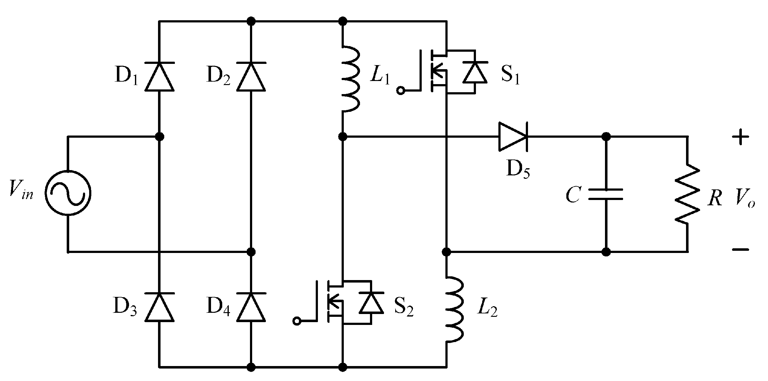
Figure 2.
The proposed bridgeless high step-up voltage gain PFC converter.

Figure 3.
The operation modes of the proposed bridgeless high step-up voltage gain PFC converter in the positive line cycle: (a) mode I; (b) mode II and (c) mode III.
Figure 3.
The operation modes of the proposed bridgeless high step-up voltage gain PFC converter in the positive line cycle: (a) mode I; (b) mode II and (c) mode III.

Figure 4.
The key time-domain waveforms of the proposed bridgeless high step-up voltage gain PFC converter.
Figure 4.
The key time-domain waveforms of the proposed bridgeless high step-up voltage gain PFC converter.
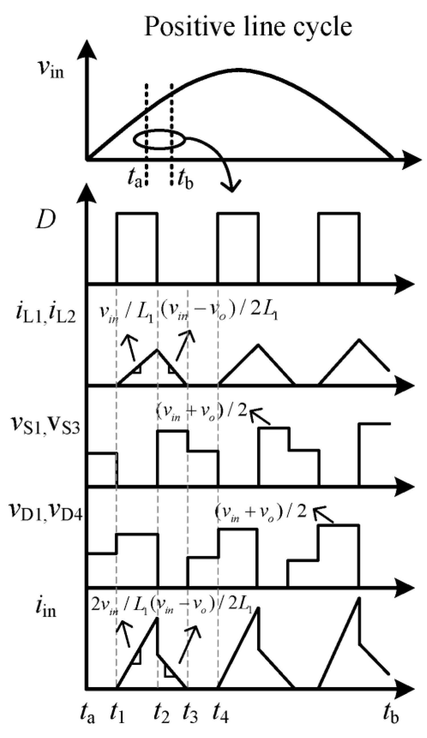
Figure 5.
The relationship of the voltage conversion ratio M and duty cycle D.
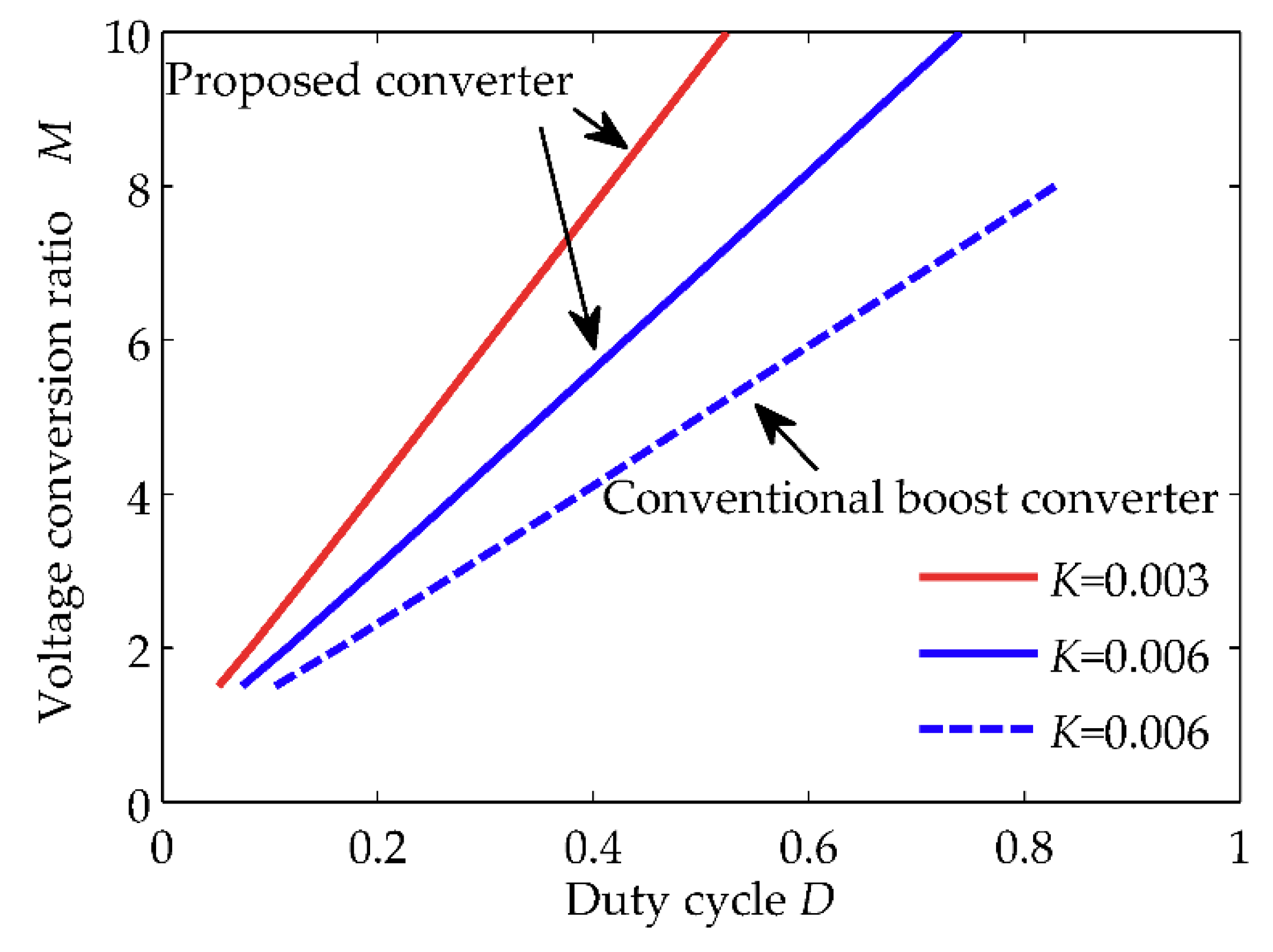
Figure 6.
The operation boundary between DCM and CCM.

Figure 7.
The calculated conduction losses of semiconductors.

Figure 8.
The control diagram of the proposed bridgeless high step-up voltage gain PFC converter.

Figure 9.
The input current waveforms after the input LC filter: (a) vin = 110 Vrms; (b) vin = 220 Vrms.
Figure 9.
The input current waveforms after the input LC filter: (a) vin = 110 Vrms; (b) vin = 220 Vrms.

Figure 10.
The key time-domain waveforms at vin = 220 Vrms.
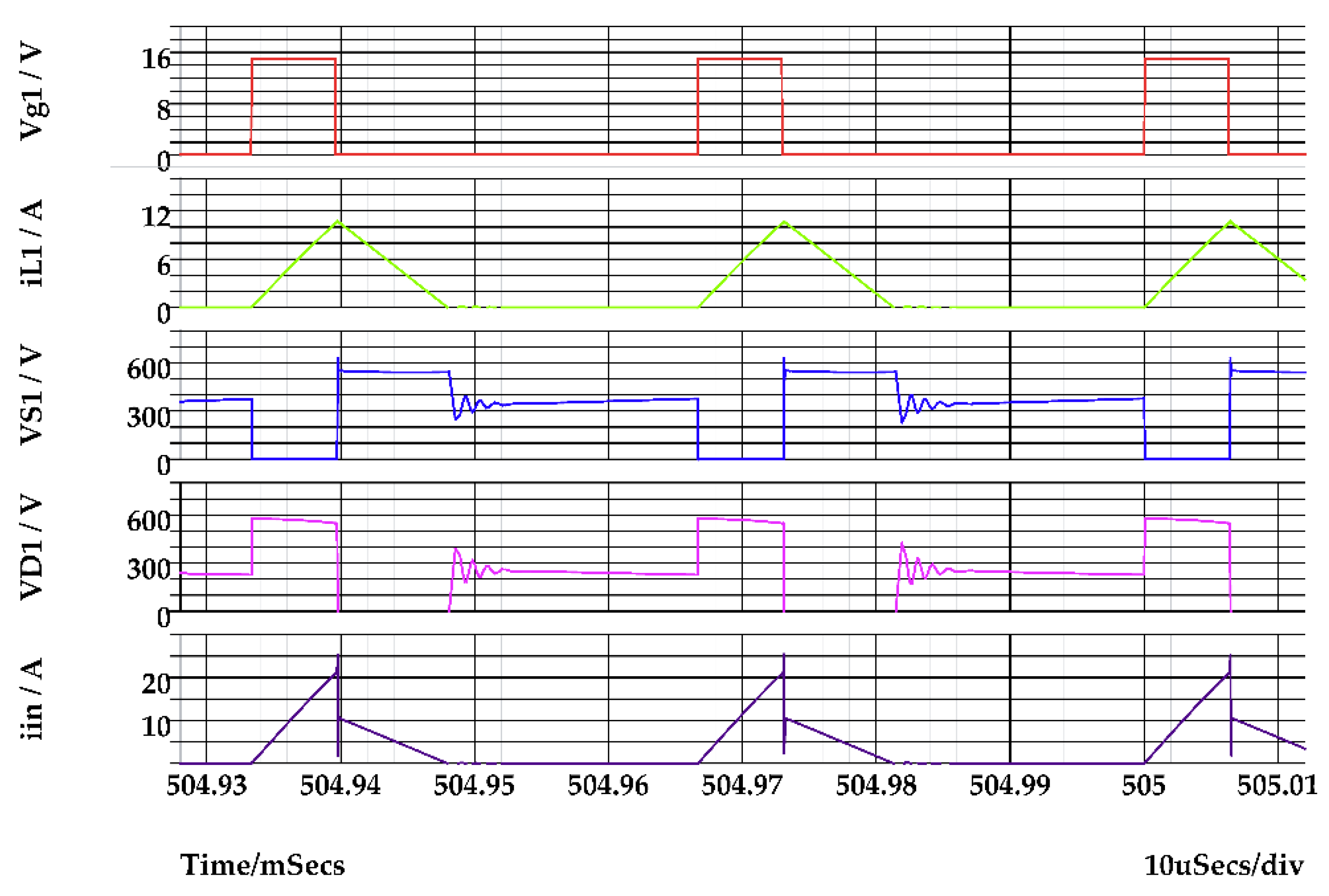
Figure 11.
The simulated PF and THD of the proposed bridgeless high step-up gain PFC converter.

Figure 12.
The simulated efficiency of the proposed bridgeless high step-up voltage gain PFC converter and its conventional bridge counterpart.
Figure 12.
The simulated efficiency of the proposed bridgeless high step-up voltage gain PFC converter and its conventional bridge counterpart.
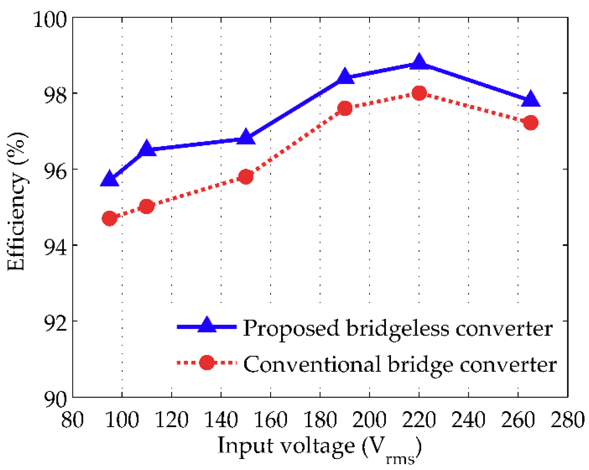
Figure 13.
The simulated input current harmonics of the proposed bridgeless high step-up voltage gain PFC converter compared with the IEC 61000-3-2 class D limits: (a) vin = 110 Vrms; (b) vin = 220 Vrms.
Figure 13.
The simulated input current harmonics of the proposed bridgeless high step-up voltage gain PFC converter compared with the IEC 61000-3-2 class D limits: (a) vin = 110 Vrms; (b) vin = 220 Vrms.


Table 1.
The voltage stress of semiconductors.
| Proposed Bridgeless PFC Converter | Conventional Bridge PFC Converter | |
|---|---|---|
| Power switch | (vm + vo)/2 | (vm + vo)/2 |
| Fast-recovery diode | vo | vm + vo |
| Slow-recovery diode | - | vm |
Table 2.
The selected components.
| Proposed Bridgeless PFC Converter | Conventional Bridge PFC Converter | |
|---|---|---|
| Power switches | SPP17N80C3 | SPP17N80C3 |
| Fast-recovery diodes | MUR490 | MUR490 |
| Slow-recovery diodes | --- | 8EWS08 |
| Output capacitor | 200µF | 200µF |
| Inductors | 200µH | 200µH |
© 2018 by the authors. Licensee MDPI, Basel, Switzerland. This article is an open access article distributed under the terms and conditions of the Creative Commons Attribution (CC BY) license (http://creativecommons.org/licenses/by/4.0/).
Share and Cite
MDPI and ACS Style
Lin, X.; Wang, F.; Iu, H.H.C. A New Bridgeless High Step-up Voltage Gain PFC Converter with Reduced Conduction Losses and Low Voltage Stress. Energies 2018, 11, 2640. https://doi.org/10.3390/en11102640
AMA Style
Lin X, Wang F, Iu HHC. A New Bridgeless High Step-up Voltage Gain PFC Converter with Reduced Conduction Losses and Low Voltage Stress. Energies. 2018; 11(10):2640. https://doi.org/10.3390/en11102640
Chicago/Turabian StyleLin, Xiang, Faqiang Wang, and Herbert H. C. Iu. 2018. "A New Bridgeless High Step-up Voltage Gain PFC Converter with Reduced Conduction Losses and Low Voltage Stress" Energies 11, no. 10: 2640. https://doi.org/10.3390/en11102640
Note that from the first issue of 2016, this journal uses article numbers instead of page numbers. See further details here.