Common Grounded H-Type Bidirectional DC-DC Converter with a Wide Voltage Conversion Ratio for a Hybrid Energy Storage System


School of Electrical and Information Engineering, Tianjin University, Tianjin 300072, China
*
Author to whom correspondence should be addressed.
Energies 2018, 11(2), 349; https://doi.org/10.3390/en11020349
Submission received: 2 January 2018
/
Revised: 22 January 2018
/
Accepted: 23 January 2018
/
Published: 2 February 2018
Abstract
:Hybrid energy storage systems (HESS) play an important role in maintaining the power balance of a direct current (DC) micro-grid. A HESS is mainly composed of high power density super-capacitors (SCs) and high energy density batteries. According to the operational requirements of an SC, a bidirectional DC-DC converter with the characteristics of a good dynamic response and a wide voltage conversion ratio is needed to interface the SC and a high-voltage DC bus. In this paper, a novel common grounded H-type bidirectional converter characterized by a good dynamic response, a low inductor current ripple, and a wide voltage conversion ratio is proposed. In addition, it can avoid the narrow pulse of pulse width modulation (PWM) voltage waveforms when a high voltage conversion ratio is achieved. All of these features are beneficial to the operation of the SC connected to a DC bus. The operating principle and characteristics of the proposed converter are presented in this paper. A 320 W prototype with a wide voltage conversion ranging from 3.3 to 8 in step-up mode and 1/8 to 1/3 in step-down mode has been constructed to validate the feasibility and effectiveness of the proposed converter.
1. Introduction
With the high penetration of direct current (DC) energy sources, storage, and loads, DC micro-grids are becoming more prevalent due to a lower number of power converters compared with an alternating current (AC) micro-grid [1,2,3]. Because of the intermittent nature of renewable energy sources and unpredictable load fluctuations in DC micro-grids, the problem of power imbalance may appear and affect the operation of DC micro-grids. Therefore, energy storage systems (ESs) are always installed to maintain the power balance of the DC micro-grid [4,5]. ESs can be divided into a power density type and an energy density type based on their characteristics [6,7]. Unfortunately, there is no single type of ES that fulfills all expected features [8]. Therefore, it is an economic and effective solution to use a hybrid energy storage system (HESS) composed by different characteristics of ESs [9,10,11]. Generally, a HESS is mainly composed of high power density super-capacitors (SCs) and high energy density batteries. It is desirable to balance the steady-state power imbalance by the batteries and compensate for the transient power imbalance by an SC with fast dynamics [12,13,14]. As a result, the degradation impact on the batteries caused by sudden load changes can be greatly reduced, and the dynamic response of the whole DC micro-grid can also be improved [15,16].
As mentioned above, high power density SCs play an important role in a HESS. However, the output voltage of an SC is relatively low and changes widely. In order to connect the SC to a high voltage level DC bus and to achieve a bidirectional power flow for the SC, a wide voltage conversion ratio bidirectional DC-DC converter is needed. Considering that the SC needs to compensate for transient power, the bidirectional DC-DC converter needs to have the feature of an outstanding dynamic response.
Many isolated and non-isolated bidirectional converters present in the literature can achieve a wide voltage conversion ratio. Due to using a high-frequency transformer, the isolated bidirectional converters can obtain a wide voltage conversion ratio in the step-up and step-down modes by adjusting the turns ratio of the transformer. Because of the use of a transformer and a high number of switching devices, the cost and switching losses of these converters will be increased and the control schemes will be more complicated [17,18,19,20]. From the viewpoint of system cost-saving and improving system efficiency, a non-isolated DC-DC converter is more suitable for HESS applications [21,22].
Research on non-isolated converters is focused on coupled-inductor, switched-capacitor, switched-inductor, voltage-multiplier, and multi-stage/-level techniques [23]. The coupled-inductor-based converter in [24] can have a higher voltage gain, and also reduce the reverse recovery losses of the diodes. However, the current ripple of the low-voltage side is relatively large, which may damage the low-voltage side source. With a simple structure, switched-capacitor converters are easy to expand. At the same time, the control methods of these converters are also simple. In different switching states, the energy of the capacitors in these converters can be delivered through different paths, making it easier for these converters to achieve a high voltage gain [25,26,27,28]. Switched-inductor converters can also achieve a wide voltage conversion ratio while avoiding extreme duty cycles. At the same time, the voltage stress of the power semiconductors in these converters can be reduced. However, more inductors affect the power density of these converters [29,30]. In [31], a new non-isolated single capacitor bidirectional DC-DC converter with a simple structure and a wide voltage conversion ratio is presented. However, the voltage stress of the power semiconductor is relatively high. A common ground switched-quasi-Z-source bidirectional DC-DC converter is presented in [32]. The advantages of this converter are a wide voltage conversion ratio and a lower voltage stress across the power switches. However, with the low voltage level (240 V) and low rated power (300 W), the volume of the capacitors (470/520 uF) and inductors (434/600 uH) is high, which results in a lower power density for this converter.
This paper presents a novel common grounded H-type bidirectional DC-DC converter, which not only achieves a wide voltage conversion ratio, but also has the advantages of a low inductor current ripple and a good dynamic response. In addition, a clamp capacitor is used in this converter to keep all of the power switches turned on and off only once during each switching period, aiming at reducing switching losses and avoiding narrow pulses of the pulse width modulation (PWM) voltage waveform at high voltage gain. These features are beneficial to improve the efficiency and reliability of this converter and its suitability for HESS applications.
As shown in Figure 1, a HESS contains a battery and an SC. The SC outputs are varying low dc voltages (25–60 V) which cannot be used directly, and must be regulated via the bidirectional converter. The proposed converter can fulfill the task well. The remainder of this paper is structured as follows. In Section 2, the novel H-type bidirectional DC-DC converter topology and operating principles are proposed. In Section 3, the characteristics of the proposed converter are analyzed and its small signal model is established. Experimental results for the proposed converter are provided in Section 4. The conclusion of this paper is introduced in Section 5.
2. Operating Principles of the Proposed Converter
2.1. Configuration of the Proposed Converter
The configuration of the proposed converter is depicted in Figure 2. This converter is composed of a capacitor-clamped H-type structure (Q1–Q4 and C1), an inductor, a power switch Q5, and two filter capacitors Chigh and Clow. To simplify the analysis, it is assumed that the capacitors and inductor are large enough and all of the power semiconductors are ideal. In order to protect the SC, the proposed converter operates in the input current continuous model (CCM).
2.2. Operating Principles
2.2.1. Step-Up Mode of the Proposed Converter
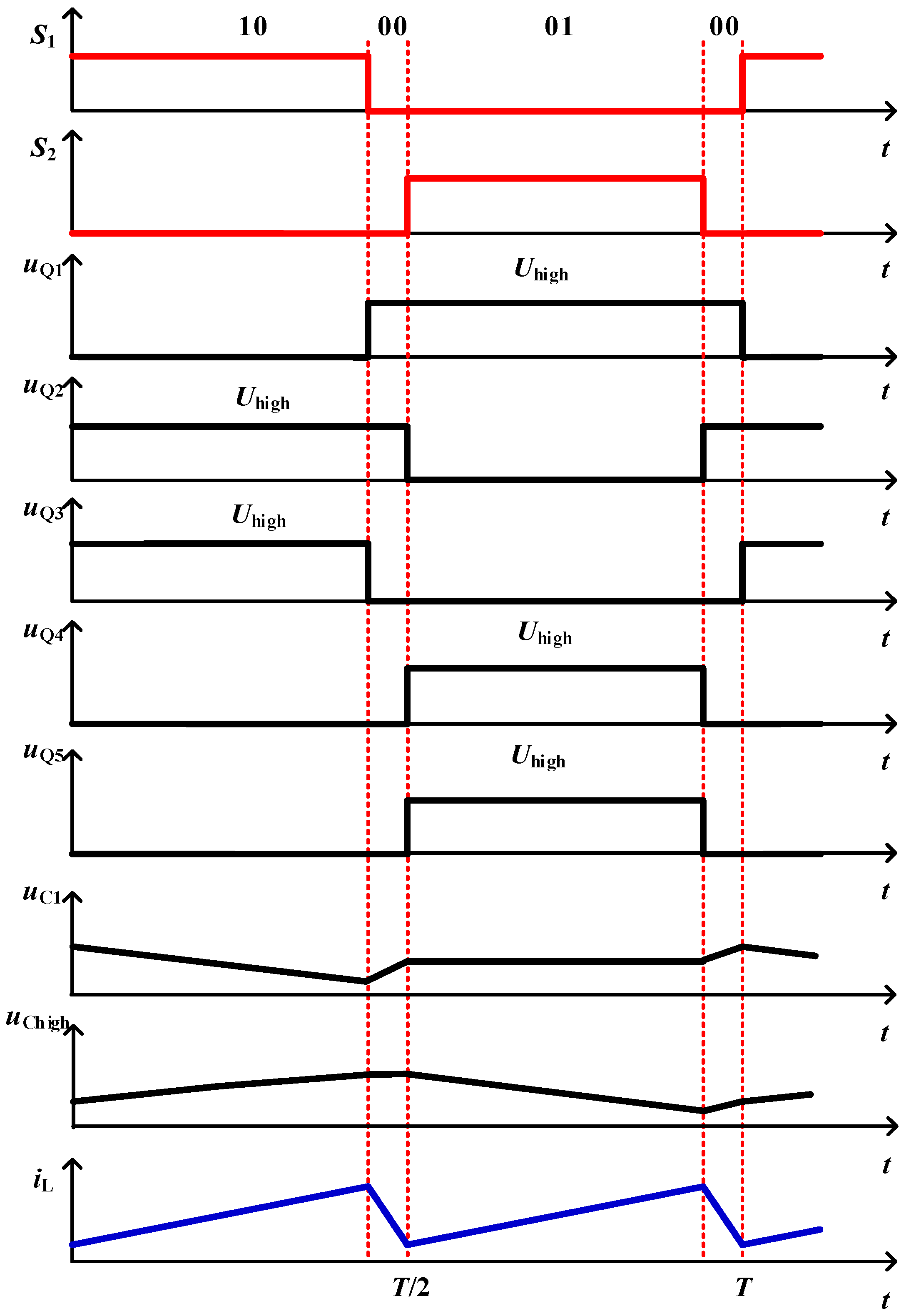
As shown in Figure 2, Ulow can be stepped-up to Uhigh by controlling the power semiconductors Q1, and Q2. The relationship between d1 and d2 can be written as d1 = d2 = dBoost, where d1 and d2 are the duty cycles of Q1 and Q2, respectively. The phase difference between the gate-driving signals S1 and S2 is 180°. During one switching period, the converter has three switching states, and their sequence is “10-00-01-00-10”. Figure 3 shows the energy flow paths and Figure 4 shows the typical waveforms. Due to using the clamp capacitor C1, all of the power semiconductors turn on and off only once during each switching period.
When S1S2 = 10: As shown in Figure 3a, where switch S1 is ON and S2 is OFF. The anti-parallel diodes of Q4 and Q5 are forward biased, while the anti-parallel diode of Q3 is reverse biased. The inductor L is charged from the input source. Current iL rises linearly. The load is supplied by C1 and Chigh. Clamp capacitor C1 maintains the forward bias of the anti-parallel diodes of Q5.
When S1S2 = 00: As shown in Figure 3b, both switches S1 and S2 are OFF. The anti-parallel diodes of Q3, Q4, and Q5 are forward biased. Capacitors C1 and Chigh are charged from L. The load is supplied by L. There is no energy exchange between capacitors C1 and Chigh.
When S1S2 = 01: As shown in Figure 3c, where switch S1 is OFF and S2 is ON. The anti-parallel diode of Q3 is forward biased, while the anti-parallel diodes of Q4 and Q5 are reverse biased. Inductor L is charged from the input source. Current iL rises linearly. The load is supplied by output capacitor Chigh. In this case, the voltage of capacitor C1 remains steady.
2.2.2. Step-Down Mode of the Proposed Converter
As shown in Figure 2, Uhigh can be stepped down to Ulow by controlling the power semiconductors Q3, Q4, and Q5. The relationship between d3, d4, and d5 can be written as d3 = d4 = d5 = dBuck, where d3, d4, and d5 are the duty cycles of Q3, Q4, and Q5, respectively. The phase difference between the gate-driving signals S3 and S4 is 180°. The gate-driving signal S5 = S4. During one switching period, the converter has three switching states, and their sequence is “111-100-111-011-111”. Figure 5 shows the energy flow paths and Figure 6 shows the typical waveforms. During each switching period, all of the power semiconductors also turn on and off once.
When S3S4S5 = 111: The switching state is shown in Figure 5a, where switches S3, S4, and S5 are ON. The anti-parallel diodes of Q1 and Q2 are forward biased. The high-voltage side Uhigh and capacitor C1 charge the inductor L, and simultaneously provide energy to the load in the low-voltage side. The current iL rises linearly.
When S3S4S5 = 100: The switching state is shown in Figure 5b, where switch S3 is ON and switches S4 and S5 are OFF. The anti-parallel diode of Q2 is forward biased, while the anti-parallel diode of Q1 is reverse biased. Inductor L provides energy to the load in the low-voltage side. The current iL decreases linearly.
When S3S4S5 = 011: The switching state is shown in Figure 5c, where switches S4 and S5 are ON and S3 is OFF. The anti-parallel diode of Q1 is forward biased, while the anti-parallel diode of Q2 is reverse biased. Inductor L provides energy to the load in the low-voltage side. The current iL decreases linearly. Capacitor C1 is charged by the high-voltage side Uhigh. The clamp capacitor C1 maintains the power switch Q5 ON.
2.2.3. Synchronous Rectification Mode of the Proposed Converter
The on-state resistance of the power switch is lower than its corresponding anti-parallel diode. As mentioned above, current flow into the corresponding anti-parallel diodes of the slave power switches will result in higher conduction losses and lower efficiency. In order to improve the efficiency, the proposed converter uses synchronous rectifier technology [33,34].
The synchronous rectification operation principle of the proposed converter is shown in Figure 7. Figure 7a shows the gate signals of S1–S5 in step-up mode and Figure 7b shows the gate signals of S1–S5 in step-down mode. In step-up mode, the current has to fully flow into the corresponding anti-parallel diodes of the slave power switches Q3, Q4, and Q5 at the dead time td. When the slave power switches are ON, the current almost flows into the MOSFETS due to their lower on-resistance as shown in Figure 7c. In step-down mode, the current flow path is the same as with the step-up mode as shown in Figure 7d. The only difference is that the slave power switches are Q1 and Q2.
When the current flows into the corresponding anti-parallel diodes of the slave power switches at dead time, the forward voltage drops of the anti-parallel diodes are close to zero. As a result, the slave active power switches turn on and turn off with zero voltage. The turn on/off losses of the slave active power switches will not be increased and the efficiency of the converter can be improved.
2.3. Control Strategy for Bidirectional Power Flow
For a HESS, the SC interface converter should be able to respond to fast bidirectional power fluctuations immediately. Therefore, a virtual capacitor droop (VCD) control is adopted for this converter. At the same time, the battery interface converter uses a virtual resistance droop (VRD) control to make the battery provide total power at steady state. Due to using the VCD and VCR control, the HESS can adapt to the distributed nature of the DC micro-grid and increase system reliability and scalability [35,36]. The specific control strategy is shown in Figure 8. As shown in Figure 8, the voltage controller is used to follow the reference voltage Uref. The voltage Uhigh and the currents ihigh-sc and ihigh-bat are obtained by the sensor samplings. ihigh-sc refers to the output current of the SC interface converter and ihigh-bat refers to the output current of the battery interface converter.
The operation modes of the proposed converter switch between the step-down and step-up modes according to the necessary conditions of a general load. The current relationship at the DC bus is expressed as
where iHESS is the equivalent load current of the HESS and can be either positive or negative. The output voltage–current (V–I) relationship of the battery interface converter under the VRD control and that of the SC interface converter under the VCD control are given by
where Rvb is the virtual resistance and Cvc is the virtual capacitance. Based on (1) and (2), the current-sharing relationship between battery and SC is derived as
3. Characteristics of the Proposed Converter
3.1. Wide Voltage Conversion Ratio
3.1.1. Voltage Conversion Ratio in Step-Up Mode
For the proposed converter shown in Figure 2, the voltage conversion ratio can be derived from the volt-sec balance of the inductor L. According to Figure 3a, Q4 and Q5 are ON, so that the voltages of C1 and Chigh are equal. In the low-voltage side current continuous model, the equations can be obtained as follows:
where UC1 is the voltage over C1. By simplifying (1), the following equation can be derived:
The voltage conversion ratio MBoost of the proposed converter is
where 0 < dBoost < 0.5.
3.1.2. Voltage Conversion Ratio in Step-Down Mode
According to Figure 5c, the power switches Q4 and Q5 are ON, so that the voltages of C1 and Chigh are equal. By applying the volt-second balance principle on L, the voltage conversion ratio in CCM can be obtained as
By simplifying (7), the following equation can be derived:
The voltage conversion ratio MBuck in step-down mode is
where 0.5 < dBuck < 1.
Under the same voltage conversion ratio, 0 shows the comparison between the proposed and the traditional two-level bidirectional converters. According to Figure 9, when the voltage conversion ratio is 8 in the step-up mode, the duty cycles of the proposed and the traditional converters are 0.4375 and 0.875, respectively; in step-down mode, when the voltage conversion ratio is 0.125, the duty cycles of the proposed and the traditional converters are 0.5625 and 0.125, respectively. Compared with the traditional converter, the proposed one can avoid the extreme duty cycle while achieving a high voltage conversion ratio. What is more, the higher the voltage conversion ratio, the closer the duty cycle is to 0.5. When the duty cycle approaches 0.5, the time used to maintain the ON and OFF state for all power semiconductors is nearly equal in each period, which is beneficial to avoid the narrow pulse of PWM voltage waveforms while the high voltage conversion ratio is achieved.
3.2. Low Inductor Current Ripple
3.2.1. The Average Inductor Current and Inductor Current Ripple in Step-Up Mode
The average inductor current can be derived from the ampere-second balance of the capacitors C1 and Chigh in CCM.
where IC1a and IC1b are the average currents across C1 in state 10 and 00, respectively. It follows from (10) that the average inductor current IL can be obtained as follows:
In the state 10, the inductor current increases linearly, and (12) can be obtained as
where f is the switching frequency and ∆iL is the inductor current ripple. It follows from (11) and (12) that the current ripple ratio rBoost of the inductor can be obtained as
where Rhigh is the equivalent load of the high-voltage side.
3.2.2. The Average Inductor Current and Inductor Current Ripple in Step-Down Mode
The average inductor current IL can be obtained as follows:
In the state 100, the inductor current decreases linearly, and (15) can be obtained as
It follows from (14) and (15) that the current ripple ratio rBuck of the inductor can be obtained as follows:
where Rlow is the equivalent load of the low-voltage side.
The inductor current ripple ratios of a traditional two-level bidirectional converter are:
where d’Boost and are the duty cycles of that converter in step-up and step-down mode, respectively. r’Boost and r’Buck are the current ripple ratios of that converter in step-up and step-down mode, respectively.
Supposing that the output power, inductor, and switching frequency of the proposed converter and the traditional two-level converter are equal, it can be obtained that
It can be concluded from (18) that the inductor current ripple ratio in the proposed converter is lower than that in the traditional two-level converter. On the other hand, if the inductor current ripple ratios are equal, the inductor of the proposed converter is only half that of the traditional one, which means that the proposed converter has outstanding dynamic response.
3.3. Good Dynamic Performance
The proposed converter can work in both the step-up and step-down modes. In order to save paper space, only the dynamic performance in step-down mode is analyzed. Before analyzing the dynamic performance, a small-signal model of step-down mode is needed.
When the proposed converter operates in the range 0.5 < dBuck < 1, the main power switches Q3, Q4, and Q5 have three effective switching states: S3S4S5 = [111, 100, 011]. uhigh, ulow, and dBuck are the input, the output, and the control variables, respectively. iL, uC1, and uClow are the state variables. r is the equivalent series resistance for C1.
When S3S4S5 = 111, the operating time of the proposed converter is (2dBuck − 1) × T. The state space average model in this operating time is
When S3S4S5 = 100, the operating time of the proposed converter is (1 − dBuck) × T. The state space average model in this operating time is
When S3S4S5 = 011, the operating time of the proposed converter is (1 − dBuck) × T. The state space average model in this operating time is
Combining (19) and (20) with (21), the average model of the proposed converter is
The state, the input, the output, and the control variables can be described by using the small-signal disturbance variables as:
where IL, UC1, UClow, Ulow, Uhigh, and DBuck are steady state components, and , , , , and are their corresponding small-signal disturbance variables.
As a result, the small-signal model of the proposed converter is
Using the parameters shown in Table 1, when the output voltage is 25 V, the control-to-output transfer function can be expressed as
Assume that the proposed converter and the traditional two-level converter have the same output power, inductor current ripple ratio, and switching frequency. Then, the inductor of the traditional two-level converter is double that of the proposed converter. The control-to-output transfer function of the traditional two-level converter in step-down mode can be expressed as
The Bode diagram of the duty cycle to output voltage open-loop transfer function is shown in Figure 10. According to Figure 10, the crossover frequency of the proposed converter is higher than that of the traditional two-level converter due to smaller inductance.
The switching frequency of the traditional two-level converter can be chosen to be five times the crossover frequency. At this point, the equivalent switching frequency of the proposed converter is twice that of the switching frequency. The side-band effect has been eliminated due to interleave control. Therefore, the crossover frequency of the proposed converter can be increased to two-fifths of f. It means that the proposed converter can push to a higher control bandwidth, which leads to better dynamic performance.
In step-up mode, small inductance and a higher equivalent switching frequency lead to better dynamic performance too.
The control-to-output transfer function derived above is helpful to design the voltage controller shown in Figure 8. The voltage controller is a PI (proportional integral) regulator and it can be expressed as
Using the control-to-output transfer function, kp and ki can be deduced.
Due to the use of the capacitor-clamped H-type structure, the proposed converter has the following advantages:
- Avoiding the narrow pulse of PWM voltage waveforms when a high voltage conversion ratio is achieved: It costs a little time to turn a power semiconductor on and off, thus the ideal narrow pulse of the PWM voltage waveform is difficult to realize. The higher the voltage conversion ratio of the proposed converter is, the closer the duty cycle is to 0.5. When the duty cycle approaches 0.5, the time used to maintain the ON and OFF state for all power semiconductors is nearly equal in each period, which is beneficial to avoid the narrow pulse of PWM voltage waveforms while a high voltage conversion ratio is achieved.
- Reducing inductor current ripple: The inductor L is charged and discharged twice during each switching period, as 0 and 0 show. With a small duty cycle in step-up mode, the charging time of the inductor is short. The charging time of the inductor in step-down mode is short too. Then, the inductor current ripple will decrease.
- Good dynamic performance: Due to using small inductance and a higher equivalent switching frequency, the proposed converter has a better dynamic performance.
3.4. Voltage and Current Stress on the Power Switches
According to the current flow path of the proposed converter in step-up mode, as shown in 0 (or the current-flow path of the step-down mode, as shown in Figure 5), using the KVL (Kirchhoff’s voltage law), the voltage stress on Q1–Q5 in the step-up and the step-down modes can be obtained as
The voltage stress on Q1–Q5 in the step-up and step-down modes is the same.
Similarly, according to current-flow path in step-up mode, as shown in Figure 3 (or the current-flow path in step-down mode, as shown in Figure 5), and the KCL (Kirchhoff’s current law), the current stress (namely average currents when the switch is ON) on Q1–Q5 in the step-up and the step-down modes can be obtained as
The current stress on Q1–Q5 in the step-up and step-down modes is also identical.
4. Experimental Result and Analyses
In order to verify the feasibility of the theoretical analysis, an experimental prototype with the parameters shown in Table 1 has been developed.
4.1. Experimental Results in the Step-Up Mode
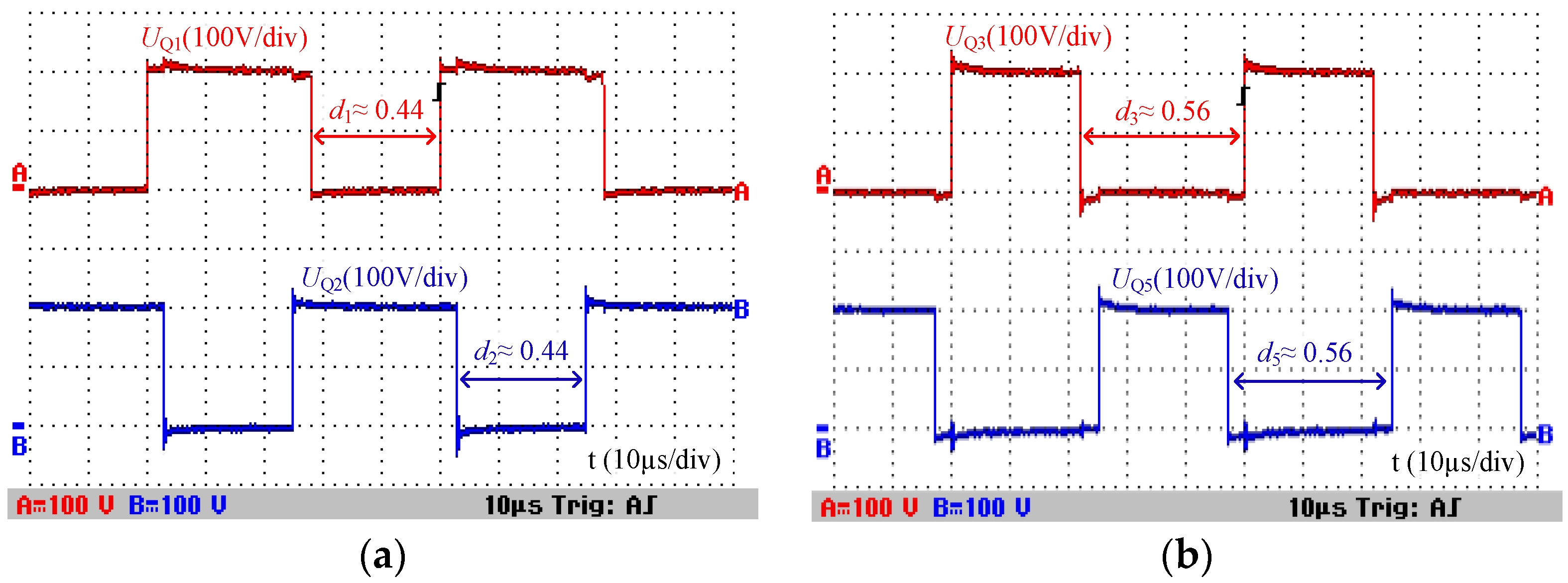
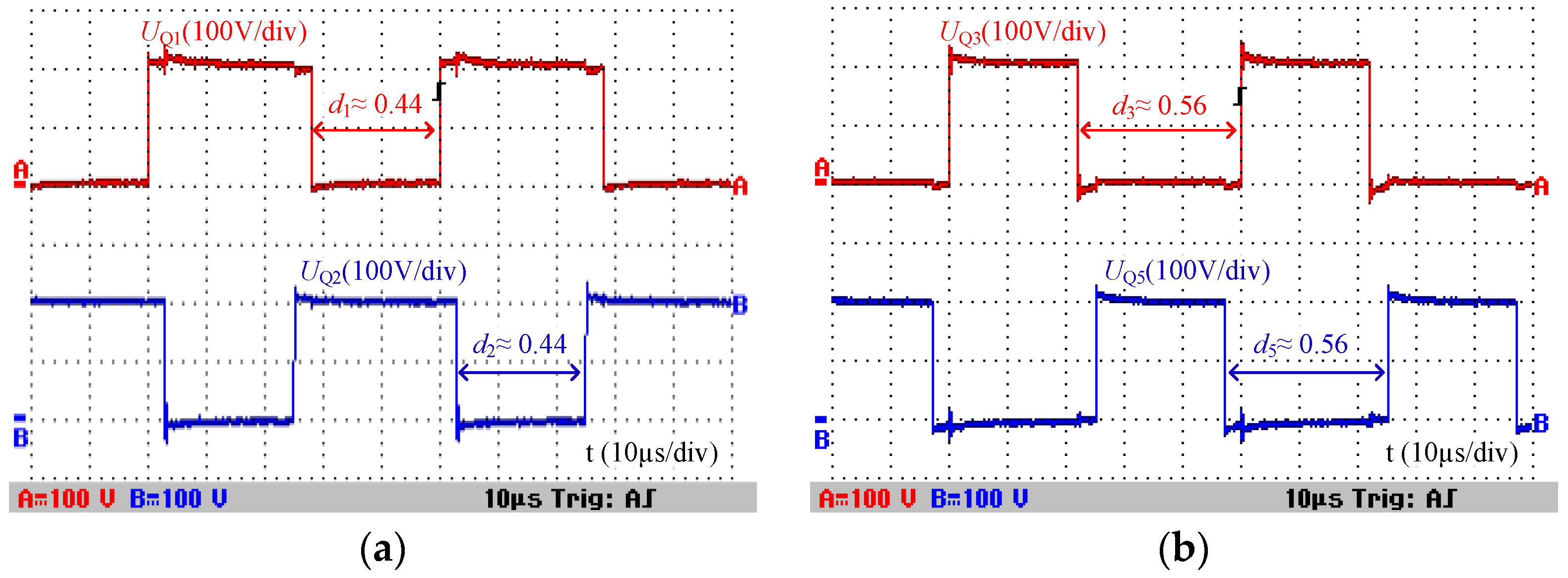
The PWM voltages of power semiconductors and the inductor current waveforms are shown in Figure 11 and Figure 12. The PWM voltage of each power semiconductor is about 200 V, approximately equal to the high-voltage side Uhigh, which validates the analysis in Section 3. According to Figure 11 and Figure 12, the voltage gain MBoost of the proposed converter is 8 and the duty cycle dBoost is about 0.44. The ON state time of the power switches Q1–Q2 is about 0.44 T and the ON state time of the power switches Q3–Q5 is about 0.56 T. At that high voltage gain, both the ON and OFF state times of those power switches are close to 0.5 T, which is effective for avoiding the narrow pulse of the PWM voltage waveforms. Due to using the synchronous rectification, the turn on and turn off of the controlled MOSFETs Q3, Q4, and Q5 realize the ZVS (zero voltage switching), e.g., the gate signal S4 and the voltage stress of Q4 as shown in Figure 13. According to Figure 11, the inductor L is charged and discharged twice during each switching period. Therefore, the equivalent switching frequency of the proposed converter is double that of the real switching frequency f. This feature is beneficial to improve the dynamic performance and reduce the inductor current ripple of this converter.
The voltage across clamp capacitor C1 is approximately 200 V, being well-consistent with Uhigh as shown in Figure 14. Therefore, in the switching state 01, the clamp capacitor C1 can maintain the forward bias of the anti-parallel diode of Q5. The feature that all power semiconductors turn on and off only once during each switching period can be achieved. This is beneficial to avoid narrow pulses of the PWM voltage waveform at high voltage gain.
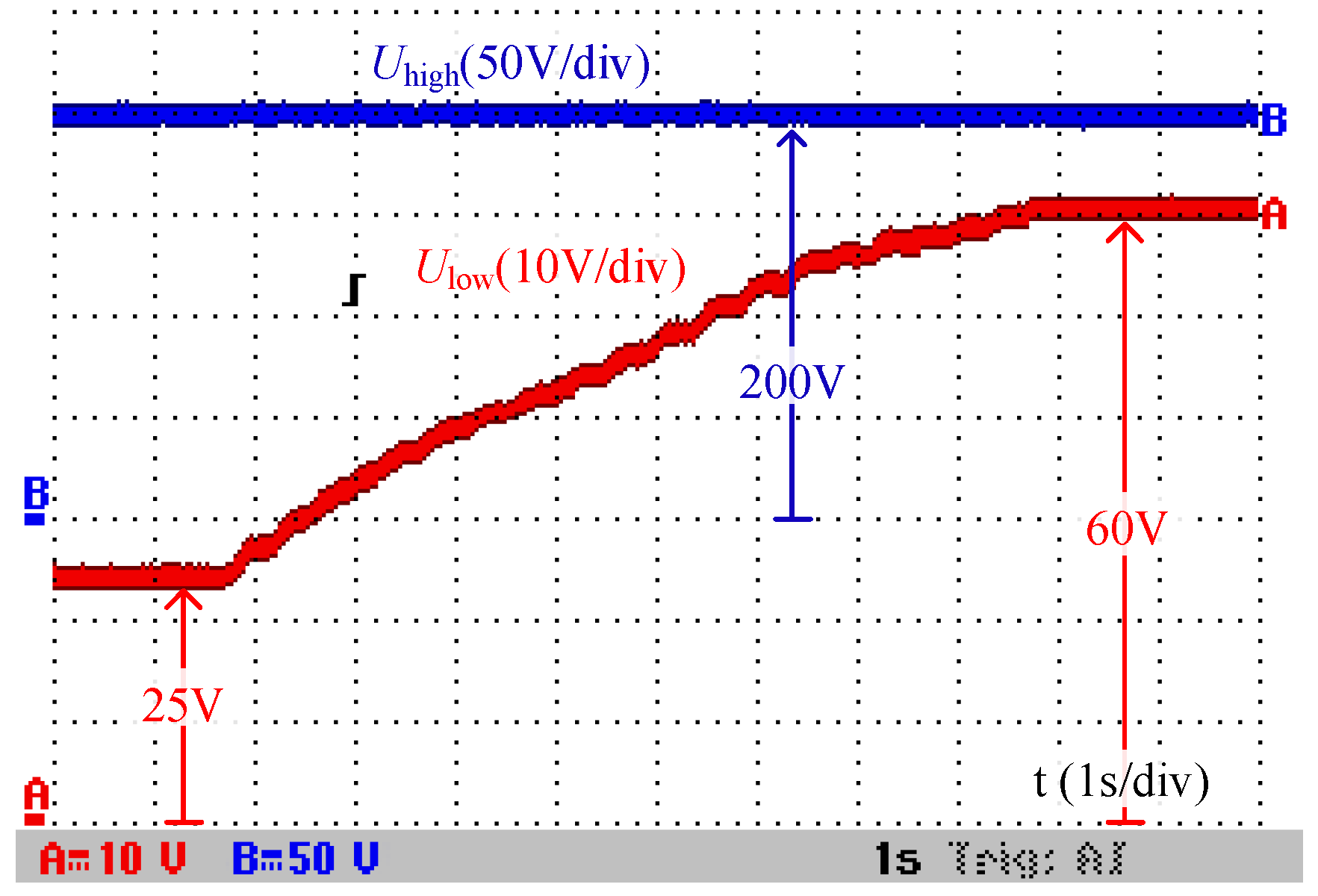
In the step-up mode, Ulow and Uhigh are the input and output voltage, respectively. The output voltage can stay around the reference value of 200 V. The output/input voltage waveforms shown in Figure 15 can be obtained when changing the input voltage dynamically. According to Figure 15, when the input voltage varies continuously from 25 V to 60 V, the output voltage can stay around 200 V. The conclusion can be obtained from Figure 15 that the proposed converter can obtain a wide voltage conversion ratio from 3.3 to 8 in step-up mode.
4.2. Experimental Results in the Step-Down Mode
Figure 16 and Figure 17 show the voltage waveforms of power semiconductors in the step-down operation mode. According to Figure 16 and Figure 17, the PWM voltage of each power semiconductor is about 200 V, approximately equaling the high-voltage side Uhigh. The voltage gain MBuck of the proposed converter is 1/8 and the duty cycle dBuck is about 0.56. The ON state time of the power switches Q3–Q5 is about 0.56 T and the ON state time of the power switches Q1–Q2 is about 0.44 T. At that high voltage conversion ratio, both the ON and OFF state times of those power switches are close to 0.5 T, which is effective for avoiding the narrow pulse of the PWM voltage waveforms. In addition, the slave power semiconductors Q1 and Q2 also acted in the synchronous rectification operation, which turned on and turned off with ZVS, e.g., the gate signal S1 and the voltage stress of Q1, as shown in Figure 18. According to Figure 16, the inductor L is also charged and discharged twice during each switching period. The dynamic performance of the proposed converter in step-down mode is also improved.
According to Figure 19, the voltage across clamp capacitor C1 is approximately 200 V, being well-consistent with Uhigh. Therefore, in the switching state 011, the clamp capacitor C1 can maintain the power switch Q5 ON. The feature that all power semiconductors turn on and off only once during each switching period can be achieved. This is also beneficial to avoid narrow pulses of the PWM voltage waveform at a high voltage conversion ratio, just like in step-up mode.
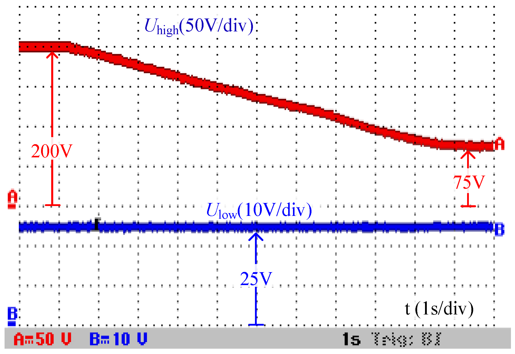
In the step-down mode, the input voltage is Uhigh and the output voltage is Ulow. The output voltage can also stay around the reference value of 25 V with the action of the voltage control loop. The output/input voltage waveforms shown in Figure 20 can be obtained when changing the input voltage dynamically. According to Figure 20, when the input voltage varies continuously from 200 V to 75 V, the output voltage can stay around 200 V. The conclusion can be obtained from Figure 20 that the proposed converter can obtain a wide voltage conversion ratio from 1/8 to 1/3 in step-down mode.
4.3. Bidirectional Power Flow Experiment
In order to verify the performance of the proposed converter in a HESS, the related experiments are carried out using the HESS shown in Figure 1. The output voltages of the SC and battery are about 42 V and 50 V, respectively, and the DC load power varies with a step change between 400 W and 650 W. The proposed converter is used as the power interface between the SC and the DC bus.
With the DC load being suddenly increased and decreased, changes in the output currents are shown in Figure 21, where ibat and isc denote the output currents of the battery and the SC, respectively. When the DC load required power changes from 400 W to 650 W suddenly, the SC compensates for the required power immediately by increasing the current isc from 0 to 6 A in 20 ms approximately, which protects the battery by avoiding a sudden change in current and prolongs its life. Gradually, the task of supplying the power shortage is transferred from the SC to the battery. The isc falls to 0 from 6 A along with the ibat rising from 8 A to 13 A. Similarly, when the DC load required power changes from 650 W to 400 W suddenly, the current isc varies from 0 to −6 A in 20 ms approximately. As a result, the current from the battery decreases from 13 A to 8 A gradually, and the current of the SC returns to 0 from −6 A. When the DC load required power suddenly increases or decreases, the SC can respond quickly to compensate for the power gap between the battery and the DC load. In this situation, the service life of the battery is extended because of the slow changes in its output current. It can be concluded from Figure 21 that the proposed converter can cooperate well in the HESS whether the load is suddenly changed or not.
The efficiencies of the proposed converter in the step-up and step-down modes are shown in Figure 22. In step-up mode, Uhigh is 200 V and Ulow varies from 25 V to 60 V continuously; in step-down mode, Ulow is 25 V and Uhigh varies from 80 V to 200 V continuously. According to Figure 22, the efficiency varies from 91.52% to 94.80% in step-up mode, which is slightly lower than that in the step-down mode (varies from 92.01% to 95.30%). With the constant load power in step-up mode, the efficiency decreases accompanied by the input voltage declining due to the increasing losses caused by the growing input current. In the step-down mode, the efficiency decreases with the increase of high side voltages. Due to the increase in the high side voltages, the voltage stresses of the power semiconductors increase. Therefore, the turn on/off losses of the power semiconductors will increase.
5. Conclusions
A new common grounded H-type bidirectional converter was proposed in this paper. It has the advantages of a wide voltage conversion ratio and a good dynamic response in both step-down and step-up operation modes. In addition, only one inductor is used in this converter, and the inductor is charged and discharged twice during each switching period, which results in a low inductor current ripple and a small size for this converter. Due to the use of a capacitor-clamped H-type structure, the proposed converter can avoid the narrow pulse of the PWM voltage waveforms while achieving a high voltage conversion ratio. Besides, the efficiency of the converter is improved because the slave active power switches turn on and turn off with zero voltage. In order to prove the feasibility, the proposed converter was implemented in the laboratory with the proper voltage conversion ratio (3.3–8 in step-up mode and 1/8–1/3 in step-down mode). A theoretical analysis and experimental results proved that the proposed converter is suitable for connecting a low-voltage SC to a high-voltage DC bus.
Acknowledgments
This research was supported by the National Key R&D Program of China (Grant: 2016YFB0900200). The authors would also like to thank the anonymous reviewers for their valuable comments and suggestions to improve the quality of the paper.
Author Contributions
Huakun Bi and Ping Wang designed the main parts of the study, including the operating principles analysis, characteristics analysis, and experiment. Zhishuang Wang helped in the hardware development, experiment, and some theoretical analysis.
Conflicts of Interest
The authors declare no conflict of interest.
References
- Han, Y.; Chen, W.; Li, Q. Energy Management Strategy Based on Multiple Operating States fora Photovoltaic/Full Cell/Energy Storage DC Microgrid. Energies 2017, 10, 136. [Google Scholar] [CrossRef]
- Whaite, S.; Grainger, B.; Kwasinski, A. Power quality in DC power distribution systems and microgrids. Energies 2015, 8, 4378–4399. [Google Scholar] [CrossRef]
- Yu, X.; She, X.; Zhou, X.; Huang, A.Q. Power management for DC microgrid enabled by solid-state transformer. IEEE Trans. Smart Grid 2014, 5, 954–965. [Google Scholar] [CrossRef]
- Hu, J.; Cheng, K.W.E. Predictive control of power electronics converters in renewable energy systems. Energies 2017, 10, 515. [Google Scholar] [CrossRef]
- Wang, B.; Sechilariu, M.; Locment, F. Intelligent DC microgrid with smart grid communications: Control strategy consideration and design. IEEE Trans. Smart Grid 2012, 3, 2148–2156. [Google Scholar] [CrossRef]
- Liu, F.; Liu, J.; Zhang, H.; Xue, D. Stability issues of Z+Z type cascade system in hybrid energy storage system (HESS). IEEE Trans. Power Electron. 2014, 29, 5846–5859. [Google Scholar] [CrossRef]
- Shim, J.W.; Kim, Y.; Cho, S.-J.; Min, S.W.; Hur, K. Synergistic control of SMES and battery energy storage for enabling dispatchability of renewable energy sources. IEEE Trans. Appl. Supercond. 2013, 23. [Google Scholar] [CrossRef]
- Xie, Q.; Wang, Y.; Kim, Y.; Pedram, M.; Chang, N. Charge allocation in hybrid electrical energy storage systems. IEEE Trans. Comput.-Aided Des. Integr. Circuits Syst. 2013, 32, 1003–1016. [Google Scholar]
- Wang, G.; Ciobotaru, M.; Agelidis, V.G. Power smoothing of large solar PV plant using hybrid energy storage. IEEE Trans. Sustain. Energy 2014, 5, 834–842. [Google Scholar] [CrossRef]
- Chen, X.Y.; Jin, J.X.; Xin, Y.; Shu, B.; Tang, C.L.; Zhu, Y.P.; Sun, R.M. Integrated SMES technology for modern power sys-tem and future smart grid. IEEE Trans. Appl. Supercond. 2014, 24. [Google Scholar] [CrossRef]
- Li, J.; Yang, Q. Design and test of a new droop control algorithm for a SMES/battery hybrid energy storage system. Energy 2017, 118, 1110–1122. [Google Scholar] [CrossRef]
- Xiao, J.; Wang, P.; Setyawan, L. Hierarchical control of hybrid energy storage system in DC microgrids. IEEE Trans. Ind. Electron. 2015, 62, 4915–4924. [Google Scholar] [CrossRef]
- Shen, J.; Khaligh, A. A supervisory energy management control strategy for a battery/ultracapacitor hybrid energy storage system. IEEE Trans. Transp. Electr. 2015, 1, 223–231. [Google Scholar] [CrossRef]
- Li, J.; Tang, Y.; Shi, J.; Gong, K.; Liu, Y.; Ren, L.; Li, J. Design and advanced control strategies of a hybrid energy storage system for the grid integration of wind power generations. IET Renew. Power Gener. 2015, 9, 89–98. [Google Scholar]
- Choi, M.-E.; Kim, S.-W.; Seo, S.-W. Energy management optimization in a battery/supercapacitor hybrid energy storage system. IEEE Trans. Smart Grid 2012, 3, 463–472. [Google Scholar] [CrossRef]
- Zhang, Y.; Jiang, Z.; Yu, X. Control strategies for battery/supercapacitor hybrid energy storage systems. In Proceedings of the 2008 IEEE Energy 2030 Conference, Atlanta, GA, USA, 17–18 November 2008; pp. 1–6. [Google Scholar]
- Inoue, S.; Akagi, H. A bidirectional dc-dc converter for an energy storage system with galvanic isolation. IEEE Trans. Power Electron. 2007, 22, 2299–2306. [Google Scholar] [CrossRef]
- Wu, K.; De Silva, C.W.; Dunford, W.G. Stability Analysis of Isolated Bidirectional Dual Active Full-Bridge DC–DC Converter with Triple Phase-Shift Control. IEEE Trans. Power Electron. 2012, 27, 2007–2017. [Google Scholar] [CrossRef]
- Li, W.; Wu, H.; Yu, H.; He, X. Isolated winding-coupled bidirectional ZVS converter with PWM plus phase shift (PPS) control strategy. IEEE Trans. Power Electron. 2011, 26, 3560–3570. [Google Scholar] [CrossRef]
- Xuewei, P.; Rathore, A.K. Novel bidirectional snubberless naturally commutated soft-switching current-fed full bridge isolated DC/DC converter for fuel cell vehicles. IEEE Trans. Ind. Electron. 2014, 61, 2307–2315. [Google Scholar] [CrossRef]
- Wai, R.J.; Wang, W.H.; Lin, C.Y. High-performance stand-alone photovoltaic generation system. IEEE Trans. Ind. Electron. 2008, 55, 240–250. [Google Scholar] [CrossRef]
- Wai, R.J.; Wang, W.H. Grid-connected photovoltaic generation system. IEEE Trans. Circuits Syst. I Regul. Pap. 2008, 55, 953–964. [Google Scholar]
- Forouzesh, M.; Siwakoti, Y.P.; Gorji, S.A.; Blaabjerg, F.; Lehman, B. Step-Up DC–DC Converters: A Comprehensive Review of Voltage Boosting Techniques, Topologies, and Applications. IEEE Trans. Power Electron. 2017, 32, 9143–9178. [Google Scholar] [CrossRef]
- Ajami, A.; Ardi, H.; Farakhor, A. A novel high step-up DC/DC converter based on integrating coupled inductor and switched-capacitor techniques for renewable energy applications. IEEE Trans. Power Electron. 2015, 30, 4255–4263. [Google Scholar] [CrossRef]
- Shen, H.; Zhang, B.; Qiu, D.; Zhou, L. A common grounded Z-source DC–DC converter with high voltage gain. IEEE Trans. Ind. Electron. 2016, 63, 2925–2935. [Google Scholar] [CrossRef]
- Zhang, G.; Li, Z.; Zhang, B.; Qiu, D.; Xiao, W.; Halang, W.A. A Z-source half-bridge converter. IEEE Trans. Ind. Electron. 2014, 61, 1269–1279. [Google Scholar] [CrossRef]
- Takiguchi, T.; Koizumi, H. Quasi-Z-source dc-dc converter with voltage-lift technique. In Proceedings of the 39th Annual Conference of the IEEE Industrial Electronics Society, IECON 2013, Vienna, Austria, 10–13 November 2013; pp. 1191–1196. [Google Scholar]
- Tang, Y.; Wang, T.; He, Y. A switched-capacitor-based active-network converter with high voltage gain. IEEE Trans. Power Electron. 2014, 29, 2959–2968. [Google Scholar] [CrossRef]
- Tang, Y.; Fu, D.; Wang, T.; Xu, Z. Hybrid switched-inductor converters for high step-up conversion. IEEE Trans. Ind. Electron. 2015, 62, 1480–1490. [Google Scholar] [CrossRef]
- Tang, Y.; Wang, T.; Fu, D. Multicell switched-inductor/switched-capacitor combined active-network converters. IEEE Trans. Power Electron. 2015, 30, 2063–2072. [Google Scholar] [CrossRef]
- Ardi, H.; Ajami, A.; Kardan, F.; Avilagh, S.N. Analysis and implementation of a no-isolated bidirectional DC–DC converter with high voltage gain. IEEE Trans. Power Electron. 2016, 63, 4878–4888. [Google Scholar] [CrossRef]
- Zhang, Y.; Liu, Q.; Li, J.; Sumner, M. A Common Ground Switched-Quasi-Z-Source Bidirectional DC-DC Converter with Wide-Voltage-Gain Range for EVs with Hybrid Energy Sources. IEEE Trans. Ind. Electron. 2017, PP. [Google Scholar] [CrossRef]
- Zhou, X.; Donati, M.; Amoroso, L. Improved light-load efficiency for synchronous rectifier voltage regulator module. IEEE Trans. Power Electron. 2000, 15, 826–834. [Google Scholar] [CrossRef]
- Wang, J.; Wu, S. A Novel Control Scheme of Synchronous Buck Converter for ZVS in Light-Load Condition. IEEE Trans. Power Electron. 2011, 26, 3265–3273. [Google Scholar] [CrossRef]
- Zhang, Y.; Li, Y. Energy Management Strategy for Supercapacitor in Droop-Controlled DC Microgrid Using Virtual Impedance. IEEE Trans. Power Electron. 2017, 32, 2704–2716. [Google Scholar] [CrossRef]
- Xu, Q.; Hu, X.; Wang, P.; Xiao, J.; Tu, P.; Wen, C.; Lee, M.Y. A Decentralized Dynamic Power Sharing Strategy for Hybrid Energy Storage System in Autonomous DC Microgrid. IEEE Trans. Ind. Electron. 2017, 64, 5930–5941. [Google Scholar] [CrossRef]
Figure 1.
Configuration of the hybrid energy storage system (HESS). DC: direct current.

Figure 2.
Configuration of the proposed converter.

Figure 3.
Energy flow paths of the proposed converter in the step-up mode; (a) S1S2 = 10; (b) S1S2 = 00; (c) S1S2 = 01.
Figure 3.
Energy flow paths of the proposed converter in the step-up mode; (a) S1S2 = 10; (b) S1S2 = 00; (c) S1S2 = 01.

Figure 4.
Typical waveforms of the proposed converter in the step-up mode.

Figure 5.
Energy flow paths of the proposed converter in the step-down mode; (a) S3S4S5 = 111; (b) S3S4S5 = 100; (c) S3S4S5 = 011.
Figure 5.
Energy flow paths of the proposed converter in the step-down mode; (a) S3S4S5 = 111; (b) S3S4S5 = 100; (c) S3S4S5 = 011.

Figure 6.
Typical waveforms of the proposed converter in the step-down mode.

Figure 7.
Synchronous rectification operation principle of the proposed converter; (a) Gate signals and dead time in step-up mode; (b) Gate signals and dead time in step-down mode; (c) Current flow path in step-up mode; (d) Current flow path in step-down mode.
Figure 7.
Synchronous rectification operation principle of the proposed converter; (a) Gate signals and dead time in step-up mode; (b) Gate signals and dead time in step-down mode; (c) Current flow path in step-up mode; (d) Current flow path in step-down mode.

Figure 8.
Control strategy for bidirectional power flow; (a) virtual capacitor droop (VCD) control; (b) virtual resistance droop (VRD) control.
Figure 8.
Control strategy for bidirectional power flow; (a) virtual capacitor droop (VCD) control; (b) virtual resistance droop (VRD) control.


Figure 9.
Comparisons of duty cycle against voltage gain; (a) Step-up mode; (b) Step-down mode.

Figure 10.
Bode diagram of the open-loop system.
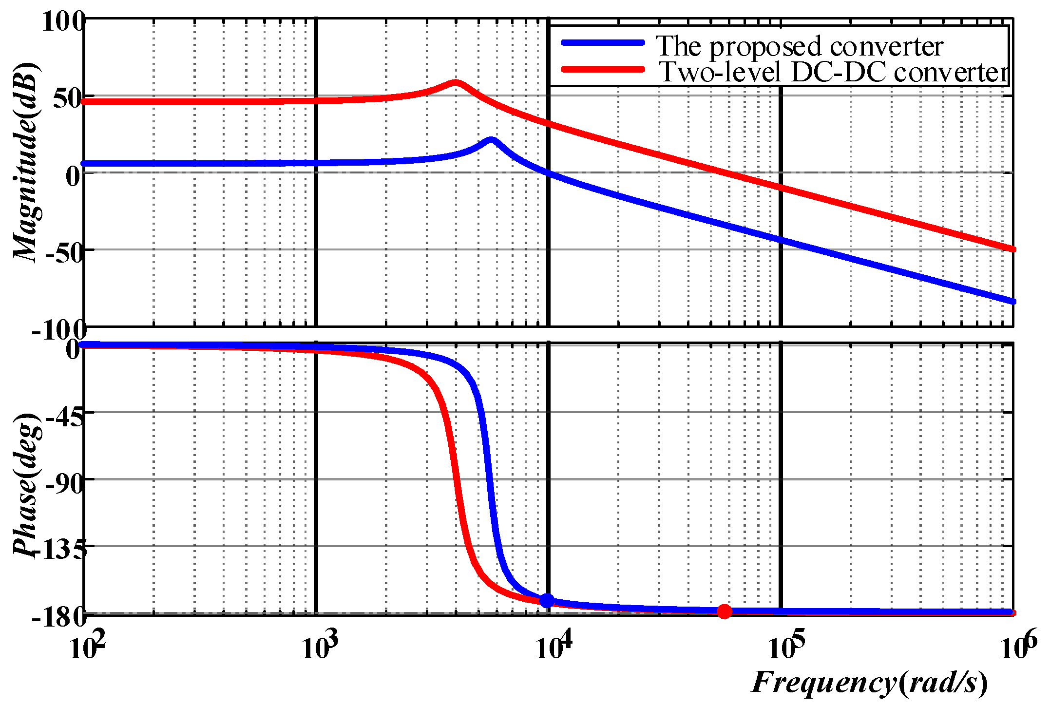
Figure 11.
PWM voltage of power semiconductor Q1 and inductor current iL.

Figure 12.
PWM voltages of power semiconductors; (a) UQ1 and UQ2; (b) UQ3 and UQ5.

Figure 13.
Voltage stress and gate signal of synchronous rectification power switch Q4.
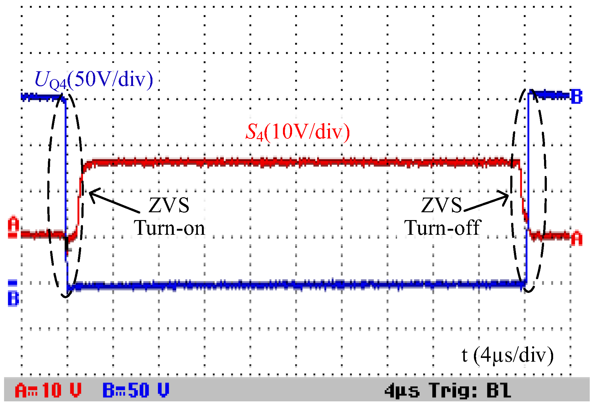
Figure 14.
Output voltage and capacitor voltage stress when Ulow = 25 V.

Figure 15.
The output voltage and the wide-range changed input voltage from 25 V to 60 V in step-up mode.
Figure 15.
The output voltage and the wide-range changed input voltage from 25 V to 60 V in step-up mode.

Figure 16.
The PWM voltage of power semiconductor Q3 and inductor current iL1.

Figure 17.
The PWM voltages of power semiconductors; (a) UQ1 and UQ2; (b) UQ3 and UQ5.

Figure 18.
Gate signal and voltage stress of synchronous rectification power semiconductor Q1.

Figure 19.
Output voltage and capacitor voltage stress when Uhigh = 200 V.

Figure 20.
The output voltage and the wide-range changed input voltage from 200 V to 75 V in step-down mode.
Figure 20.
The output voltage and the wide-range changed input voltage from 200 V to 75 V in step-down mode.

Figure 21.
The output current waveforms of the battery and the super-capacitor (SC).

Figure 22.
Efficiencies with different input voltages; (a) Step-up mode; (b) Step-down mode.


Table 1.
Experiment parameters.
| Parameters | Values |
|---|---|
| Rated power Pn | 320 W |
| Storage/filter capacitor Clow and Chigh | 260 uF |
| Clamp capacitor C1 | 260 uF |
| Storage/filter inductor L | 114 uH |
| High-voltage side Uhigh | 200 V |
| Low-voltage side Ulow | 25~60 V |
| Switching frequency f | 20 kHz |
| Power semiconductors Q1–Q5 | IXTH 88N30P |
© 2018 by the authors. Licensee MDPI, Basel, Switzerland. This article is an open access article distributed under the terms and conditions of the Creative Commons Attribution (CC BY) license (http://creativecommons.org/licenses/by/4.0/).
Share and Cite
MDPI and ACS Style
Bi, H.; Wang, P.; Wang, Z. Common Grounded H-Type Bidirectional DC-DC Converter with a Wide Voltage Conversion Ratio for a Hybrid Energy Storage System. Energies 2018, 11, 349. https://doi.org/10.3390/en11020349
AMA Style
Bi H, Wang P, Wang Z. Common Grounded H-Type Bidirectional DC-DC Converter with a Wide Voltage Conversion Ratio for a Hybrid Energy Storage System. Energies. 2018; 11(2):349. https://doi.org/10.3390/en11020349
Chicago/Turabian StyleBi, Huakun, Ping Wang, and Zhishuang Wang. 2018. "Common Grounded H-Type Bidirectional DC-DC Converter with a Wide Voltage Conversion Ratio for a Hybrid Energy Storage System" Energies 11, no. 2: 349. https://doi.org/10.3390/en11020349
Note that from the first issue of 2016, this journal uses article numbers instead of page numbers. See further details here.