Article

A Single-Stage Asymmetrical Half-Bridge Flyback Converter with Resonant Operation

1
Graduate Institute of Electronics Engineering, National Taiwan University, Taipei 106, Taiwan
2
Department of Electronic and Computer Engineering, National Taiwan University of Science and Technology, Taipei 106, Taiwan
*
Author to whom correspondence should be addressed.
Energies 2018, 11(7), 1721; https://doi.org/10.3390/en11071721
Submission received: 8 May 2018 / Revised: 17 June 2018 / Accepted: 26 June 2018 / Published: 1 July 2018
(This article belongs to the Section F: Electrical Engineering)

Abstract

:
This paper proposes a single-stage asymmetrical half-bridge fly-back (AHBF) converter with resonant mode using dual-mode control. The presented converter has an integrated boost converter and asymmetrical half-bridge fly-back converter and operates in resonant mode. The boost-cell always operates in discontinuous conduction mode (DCM) to achieve high power factor. The presented converter operates simultaneously using a variable-frequency-controller (VFC) and pulse-width-modulation (PWM) controller. Unlike the conventional single-stage design, the intermediate bus voltage of this controller can be regulated depending on the main power switch duty ratio. The asymmetrical half-bridge fly-back converter utilizes a variable switching frequency controller to achieve the output voltage regulation. The asymmetrical half-bridge fly-back converter can achieve zero-voltage-switching (ZVS) operation and significantly reduce the switching losses. Detailed analysis and design of this single-stage asymmetrical half-bridge fly-back converter with resonant mode is described. A wide AC input voltage ranging from 90 to 264 Vrms and output 19 V/120 W prototype converter was built to verify the theoretical analysis and performance of the presented converter.

1. Introduction

A conventional power supply was designed with a two-stage scheme that can be divided into two parts. The first stage achieves power-factor-correction (PFC) to reduce the input current harmonics. The second stage is a DC/DC converter that regulates the output voltage. However, the two-stage scheme has several defects, such as high cost and power supply system complexity. In recent years, a single-stage scheme was proposed [1,2,3,4,5] that integrates a boost stage and a DC/DC stage to share a common switch. The boost-cell stage operates in discontinuous conduction mode (DCM) to provide high power factor while the DC/DC stage can be responsible for output voltage regulation. Unfortunately, the single-stage scheme presents major problems in which the intermediate bus voltage cannot be regulated, such as the boost integrated flyback rectifier energy DC/DC (BIFRED) converter, single-stage fly-back converter and single-stage LLC resonant converter [6,7,8,9,10]. When voltage is input for universal applications, the intermediate bus voltage could be as high as 1000 V, causing difficulty in selecting converter components, with voltage stress issues throughout the capacitors and switches. The wide intermediate bus voltage variation will cause output voltage regulation design difficulty and also cause lower conversion efficiency though the DC/DC stage. The single-stage scheme intermediate bus voltage cannot be regulated at light loads and universal input voltage. The zero-voltage-switching (ZVS) fly-back converters have been used widely in industry and are suitable for low-to-medium power applications, such as LED-driver and desktop computer power supplies. Various kinds of ZVS schemes have been proposed, such as the active-clamp network and asymmetrical half-bridge circuit [11,12]. The active-clamp fly-back converter [13] employs the active clamp network to achieve ZVS operation; however, the voltage stresses on the switches are greater than input voltage which will cause high conduction losses in the power switches. The asymmetrical half-bridge fly-back converter (AHBF) with resonant mode [14,15,16,17,18,19,20] was developed to achieve ZVS and reduce the voltage stresses on the switches to less than that of the active-clamp fly-back converter, so the power density and conversion efficiency can be effectively increased. Furthermore, it can operate under changed duty cycles or variable switching frequencies for regulated output voltage.
This paper proposes a new single-stage asymmetrical half-bridge fly-back converter with resonant mode. The proposed converter integrates a boost converter and an asymmetrical half-bridge fly-back converter with resonant mode using dual-mode control. The converter intermediate bus voltage can be regulated by the pulse-width-modulation control (PWM). The variable-frequency-controller (VFC) can regulate the converter output voltage. Therefore, this proposed converter can operate in universal input voltage and solves the voltage stress issues throughout the capacitors and switches. The proposed converter utilizes the ZVS technique to decrease the switching losses, resulting in high conversion efficiency. The operational principle for the proposed converter is analyzed, a prototype converter with AC input voltage of 90–264 Vrms and output voltage/current of 19 V/8 A is built to verify the analytical results.

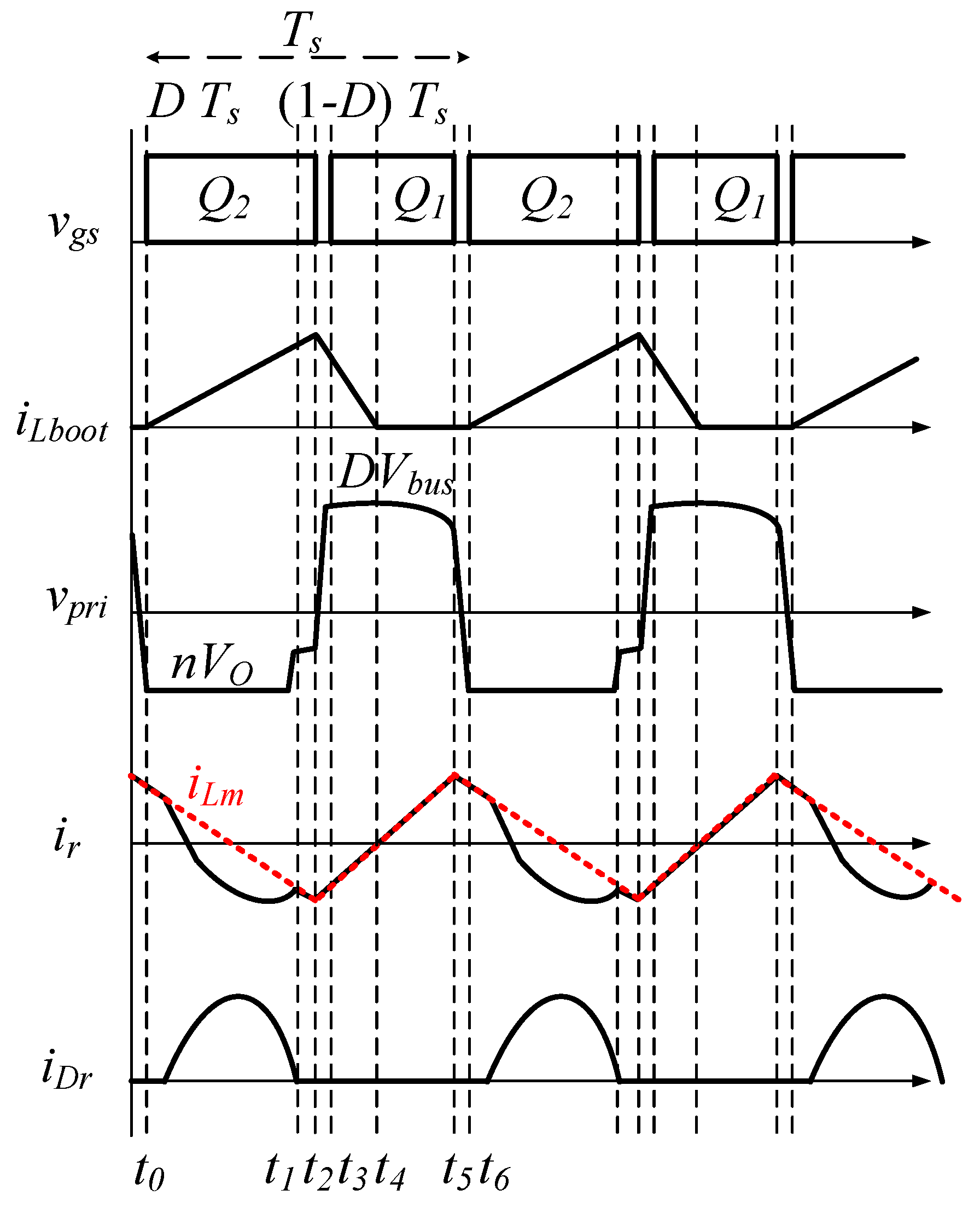
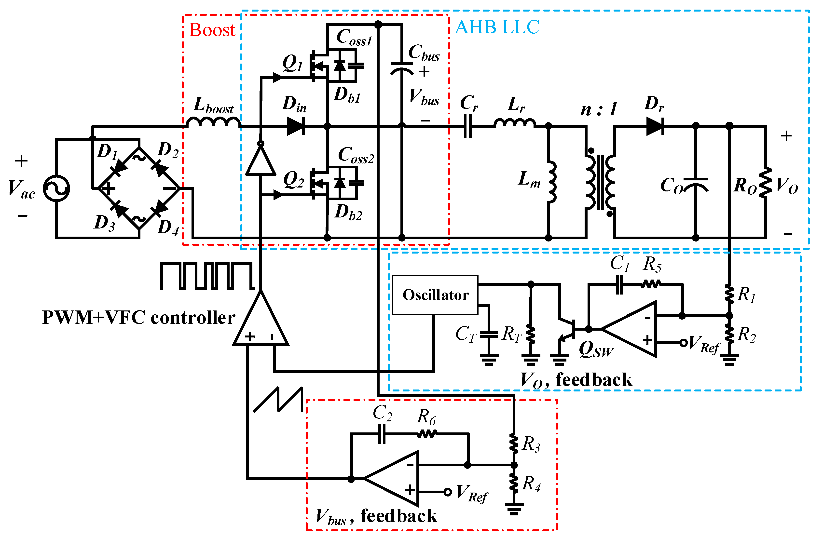
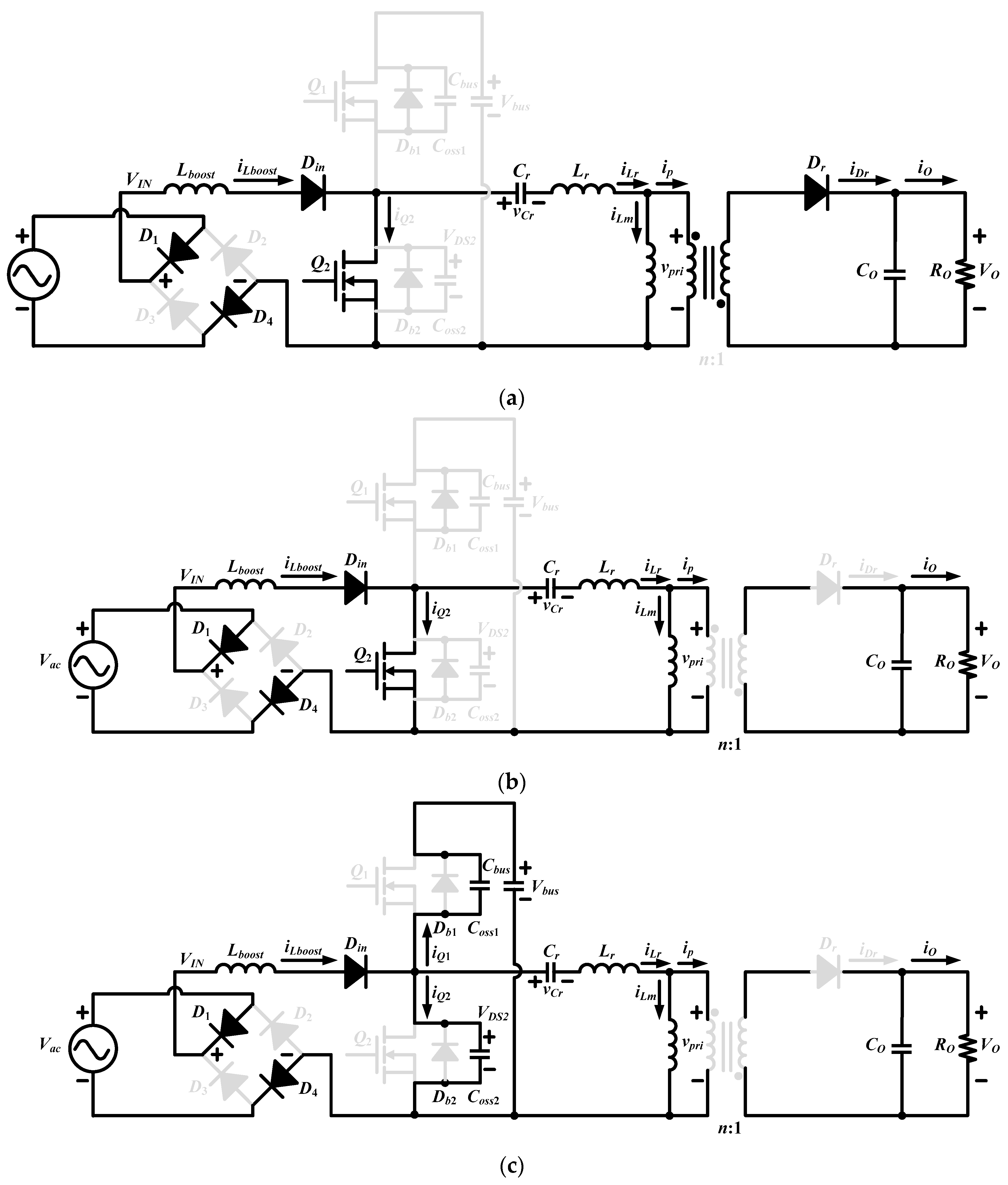
2. Circuit Description and Principle Operation of Proposed Converter

Figure 1 shows the circuit configuration for the single-stage asymmetrical half-bridge fly-back converter with resonant mode. The primary switches Q1 and Q2 operate at asymmetrical duty ratio. Db1 and Db2 are the anti-paralleled power MOSFETs. The primary side diode Din is a braking diode. The Lboost is a boost-cell inductor. The resonant inductor Lr, resonant capacitor Cr and magnetizing inductor Lm for are the resonant tank for the asymmetrical half-bridge fly-back converter. The secondary diode Dr is a rectifier diode, the Cbus is boost cell output capacitor and CO is the asymmetrical half-bridge fly-back converter output capacitor.
The following assumptions were made to analyze the proposed single-stage asymmetrical half-bridge fly-back converter:
-
These conduction losses of all switches, diodes and layout traces, and the copper losses of the transformer are neglected.
-
The turn ratio of the transformer windings is n = N1/N2.
-
The resonant inductor Lr is composed of a leakage inductor and external inductor, where Lr = Leakage + Lex.
-
The conduction times for Q1 are (1 − D)Ts and Q2 is DTs, respectively, where D is the duty cycle for Q2, and Ts denotes the switching period. In addition, the dead time is much smaller than that other of conduction times.
-
In the steady state the bus capacitance Cbus and output capacitance CO are large enough so that the bus voltage Vbus and output voltage VO are a constant value.
Both the boost-cell stage and asymmetrical half-bridge fly-back converter stage share the common switches Q1 and Q2, and furthermore there is bus capacitor Cbus between the two stages. The boost-cell stage was presented in [21]. When the switch Q2 is turned on and the switch Q1 is turned off, this results in a positive voltage VLboost = VIN across the inductor Lboost causing a linear increase in the inductor current iLboost. Conversely, when the switch Q1 is turned on and the switch Q2 is turned off, the inductor Lboost is releases energy to the bus capacitor Cbus. Therefore, from the flux-balance of Lboost under the steady-state, Vbus can be determined as:
V b u s V I N = 1 2 + 1 + 2 D 2 R L b u s L f s 2
In the DC/DC stage, when the switch Q1 is turned on, the intermediate bus voltage Vbus will charge Cr, Lr and Lm. Conversely, when the switch Q2 is turned on, the secondary diode Dr conducts and Lm is releases energy to the output load. When the asymmetrical half-bridge fly-back converter operates in resonant mode, the voltage transfer ratio can be expressed as:
M = n V O V b u s = ( 1 D ) 1 cos [ ω r ( D f s ) ] Z r ω r 1 D ω r [ 1 n 2 R o + D 2 L m f s ] sin [ ω r ( D f s ) ] + ( 1 D ) 2 n 2 R o f s + 1 cos [ ω r ( D f s ) ] Z r ω r
where:
ω r = 1 C r L r
Z r = L r C r
From Equation (2), the voltage transfer ratio of the asymmetrical half-bridge fly-back converter includes relation between the duty ratio D and switching frequency fs simultaneously. Figure 2 shows the relation between the duty ratio D, switching frequency fs and voltage transfer ratio. It shows that when the duty-ratio D is decreased from 0.35 to 0.65, to maintain fixed voltage gain, the switching frequency can shift from fc to fa correspondingly. However, Figure 2 also shows that when the switching frequency fs or duty ratio D decreases the voltage gain will be increased. In contrast, when the switching frequency fs or duty ratio D increase, the voltage gain will be decreased.
From Figure 1, the resistors R3 and R4 can measure output voltage Vbus and it can be to through the compensator, which is composed of C2, R6 and operational amplifier (OPA). The output voltage of compensator can provide a DC level for PWM + VFC controller, so that the duty ratio can be changed according to Vbus. On the other hand, the Q2 is the boost-cell stage main switch, therefore the intermediate bus voltage Vbus is regulated by the D to Q2 duty ratio. Unfortunately, changing the D to Q2 duty ratio will affect the asymmetrical half-bridge fly-back converter output voltage. For example, when the D to Q2 duty ratio is increased, the asymmetrical half-bridge fly-back converter output voltage will decrease. Conversely, when the D to Q2 duty ratio is decreased, the asymmetrical half-bridge fly-back converter output voltage will increase. To overcome the change in D to Q2 duty ratio causing unstable asymmetrical half-bridge fly-back converter output voltage, a VFC has been added to the feedback control loop.
From the section of VO-feedback of Figure 1, the resistors R1 and R2 can measure output voltage VO, and the feedback-voltage can be to through the compensator, which is composed of C1, R5 and OPA. Therefore, the output of OPA will adjust QSW at basis-terminal voltage, so that the oscillator can be changed the frequency of saw-tooth wave in output-terminal. When the asymmetrical half-bridge fly-back converter output voltage is decreased, the switching frequency fs will decrease to provide larger voltage gain for regulated output voltage. Conversely, when the output voltage is increased, the switching frequency fs will be increased to provide lower voltage gain. According to the above analysis, the intermediate bus voltage Vbus and output voltage VO of the proposed converter can be regulated simultaneously from the PWM control and VFC.
Figure 3 depicts the key waveforms of the proposed single-stage asymmetrical half-bridge fly-back converter with resonant mode. Six states are required to complete a switching cycle. The conduction paths for each operating state are illustrated in Figure 4.
Mode 1 [t0, t1]:
As shown in Figure 4, Q2 is turned on with the ZVS operating condition. In the meantime the rectifier diode Dr is conducted and the energies stored in the transformer magnetizing inductors are transferred to the output load. The output voltage is reflected to the primary side, therefore, the primary transformer is clamped to −nVO, and iLm decreases linearly. During this period, the resonant inductor Lr and resonant capacitor Cr begin to resonate. On the other hand, the diode Din is conducted and the voltage across the input inductor Lboost is equal to the input voltage VIN so the input inductor current iLboost increases linearly. The input current iLboost can be expressed as:
i L b o o s t ( t ) = V b u s L b o o s t ( t t 0 )
The resonant inductor current iLr and the resonant capacitor voltage vCr are given as:
i L r ( t ) = i L r ( t 0 ) cos [ ω r ( t t 0 ) ] v C r ( t 0 ) + n V o Z r sin [ ω r ( t t 0 ) ]
v C r ( t ) = n V O + [ v C r ( t 0 ) + n V O ] cos [ ω r ( t t 0 ) ] + Z r i L r ( t 0 ) sin [ ω r ( t t 0 ) ]
The magnetizing current iLm of transformer can be expressed as
i L m ( t ) = i L m ( t 0 ) n V O ( t t 0 ) L m
This interval is ended when iLr equals iLm at t1.
Mode 2 [t1, t2]:
At time t1 the input inductor current iLboost increases linearly. The resonant inductor current iLr is the same as the magnetizing current iLm therefore, no current is transferred to the secondary side so the rectifier diode Dr is turned off. During this mode, the resonant circuit is composed of Cr, Lr and Lm. Moreover, Lm is equal to series with Lr and Lm is much larger than Lr, so that the resonant cycle is much longer than the previous state. The iLm, iLr and vCr are expressed as:
i L r ( t ) = i L r ( t 1 ) cos [ ω r 2 ( t t 1 ) ] ω r 2 C r v c r ( t 1 ) sin [ ω r 2 ( t t 1 ) ]
v C r ( t ) = v C r ( t 1 ) cos [ ω r 2 ( t t 1 ) ] + L m i L r ( t 1 ) ω r 2 sin [ ω r 2 ( t t 1 ) ] + L r i L r ( t 1 ) ω r 2 sin [ ω r 2 ( t t 1 ) ]
i L m ( t ) = i L r ( t )
here:
ω r 2 = 1 C r ( L m + L r )
When Q2 is turned off this interval is ended.
Mode 3 [t2, t3]:
The mode begins when Q2 is turned off at t = t2. The magnetizing current iLm charges the Q2 junction capacitors and discharges the Q1 junction capacitors until the Q2 junction capacitors equal Vbus and the Q1 body diode conducts. Therefore, at time t3, Q1 can be turned on to achieve ZVS. During this period, which is used to allow enough time to achieve ZVS, as well as prevent shoot through in the two switches, the iLr and vCr are expressed as
i L r ( t ) = i L r ( t 2 ) cos [ ω r 1 ( t t 2 ) ] ω r 2 C r v c r ( t 1 ) sin [ ω r 1 ( t t 2 ) ]
v C r ( t ) = i L r ( t 2 ) ω r 1 C r sin [ ω r 1 ( t t 2 ) ] + v c r ( t 2 ) cos [ ω r 1 ( t t 2 ) ]
where:
ω r 1 = 1 ( L m + L r ) ( C e q | | C r ) C o s s 1 = C o s s 2 ; C e q = C o s s 1 = C o s s 2
The input current iLboost can be expressed as:
i L b o o s t ( t ) = V I N V b u s L b o o s t ( t t 2 )
Mode 4 [t3, t4]:
In this state, Q1 is turned on which carries the resonant inductor current iLr and input inductor current iLboost. The voltage across the input inductor Lboost is about (VINVbus) so the input inductor current iLboost linearly decreasing. Referring to Figure 4d, the rectifier diode Dr is reverse-biased and in the meantime the input energy is stored in the primary magnetizing inductance Lm, while the output capacitors CO provide energy to the output load. The resonant inductor current iLr, magnetizing inductance current iLm and resonant capacitors voltage vCr can be expressed as:
i L r ( t ) = i L r ( t 3 ) cos [ ω r 2 ( t t 3 ) ] + ω r 2 C r v b u s sin [ ω r 2 ( t t 3 ) ] ω r 2 C r v c r ( t 3 ) sin [ ω r 2 ( t t 3 ) ]
v C r ( t ) = v c r ( t 3 ) + i L r ( t 3 ) cos [ ω r 2 ( t t 3 ) ] + ω r 2 C r v b u s sin [ ω r 2 ( t t 3 ) ] ω r 2 C r v c r ( t 3 ) sin [ ω r 2 ( t t 3 ) ]
i L m ( t ) = i L r ( t )
The input current iLboost are given as:
i L b o o s t ( t ) = V I N V b u s L b o o s t ( t t 3 )
When input current iLboost reach zero level, this interval is ended.
Mode 5 [t4, t5]:
During this stage, Q1 remains turned on so that the direction of iLr is reversed. As with Stage 4 the primary magnetizing inductance Lm stores energy and the output capacitors CO continue to provide energy through the output load. The current in Lboost stays at zero (DCM operation) so the PFC feature can be achieved. In the meantime, diode Din is in reverse bias. The resonant inductor current iLr, magnetizing inductance current iLm and the resonant capacitor voltage vCr are given as:
i L r ( t ) = i L r ( t 4 ) cos [ ω r 2 ( t t 4 ) ] + ω r 2 C r v b u s sin [ ω r 2 ( t t 4 ) ] ω r 2 C r v c r ( t 4 ) sin [ ω r 2 ( t t 4 ) ]
v C r ( t ) = v c r ( t 4 ) + i L r ( t 4 ) cos [ ω r 2 ( t t 4 ) ] + ω r 2 C r v b u s sin [ ω r 2 ( t t 4 ) ] ω r 2 C r v c r ( t 4 ) sin [ ω r 2 ( t t 4 ) ]
i L m ( t ) = i L r ( t )
where:
ω r 2 = 1 C r ( L m + L r )
When Q1 turned off, this interval is ended.
Mode 6 [t5, t6]:
In this stage, Q1 and Q2 are turned off and the input current iLboost remains at zero, while the output capacitors continue to provide energy through the output load. At this interval, the resonant current iLr charges the Q1 junction capacitors and discharges the Q2 junction capacitors. When Q1 equals Vbus and the body diode across Q2 conducts, this interval is ended and the operating state returns to Stage 1 to begin the next switching cycle. The resonant inductor current iLr, magnetizing inductance current iLm and resonant capacitor voltage vCr can be expressed as:
i L r ( t ) = i L r ( t 5 ) cos [ ω r 1 ( t t 5 ) ] + ω r 1 C r v C r ( t 5 ) sin [ ω r 1 ( t t 5 ) ]
v C r ( t ) = I L r ( t 5 ) ω r 1 C r sin [ ω r 1 ( t t 5 ) ] + v C r ( t 5 ) cos [ ω r 2 ( t t 5 ) ]
i L m ( t ) = i L r ( t )
When Stage 6 ends the operating state returns to Stage 1 and the next switching cycle begins.

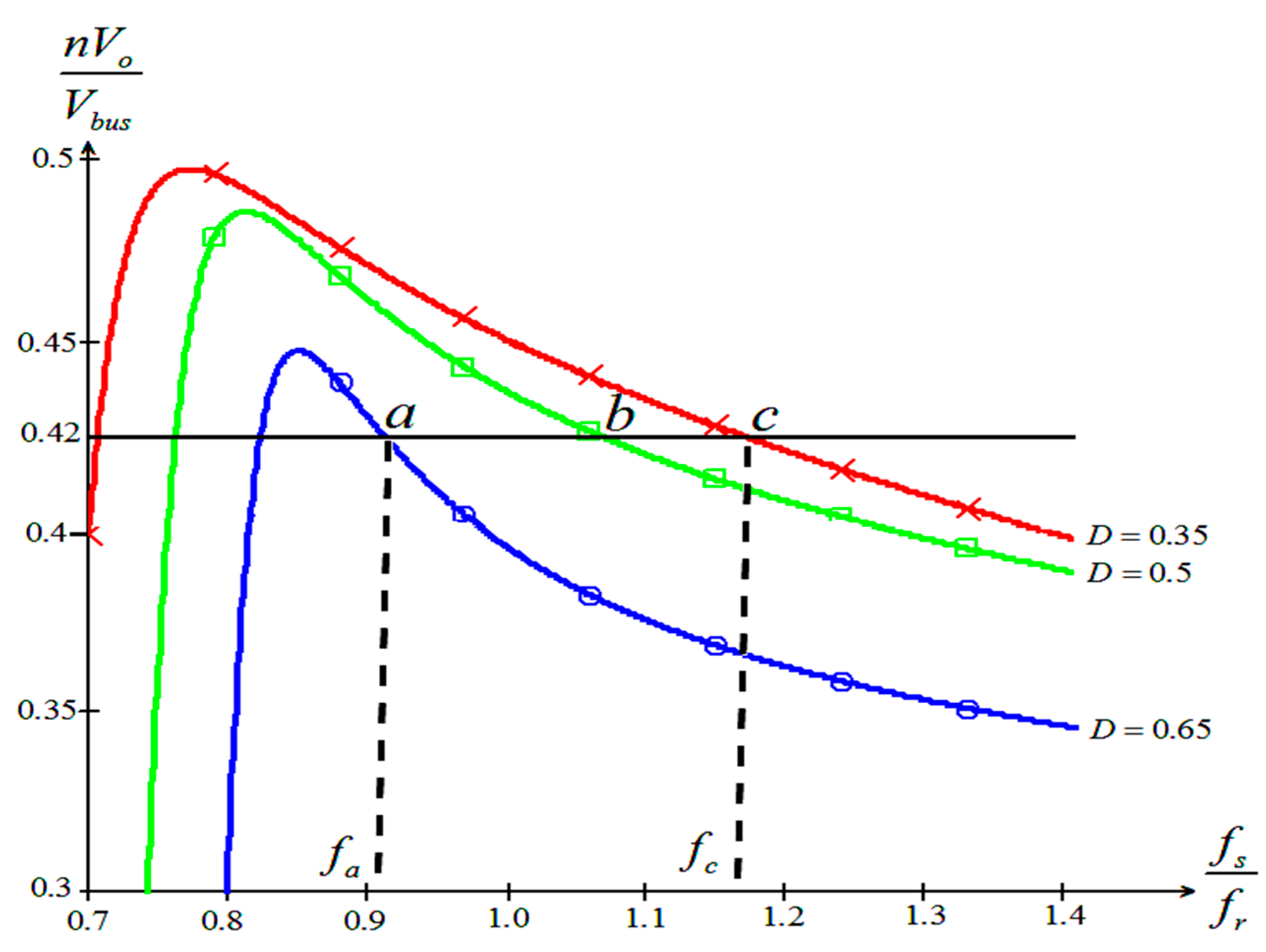
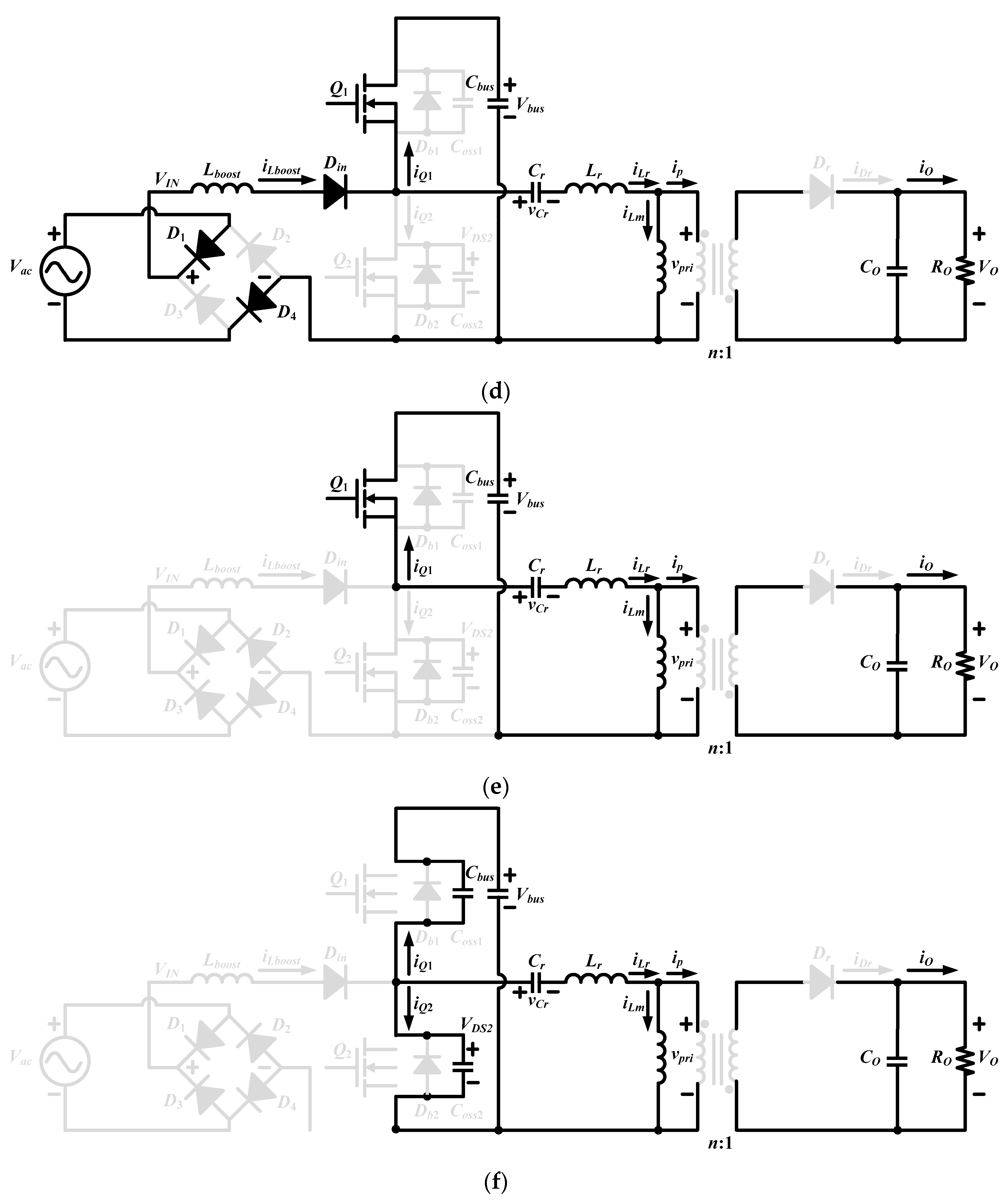
3. Circuit Design for the Proposed Converter

Dmax is the maximum duty cycle for the proposed converter. For to achieve high power-factor the input inductor current must be operated in DCM so the input inductor Lboost can be expressed as:
L b o o s < V b u s T s 2 i I N peak f s min ( D max ) ( 1 D max ) 2
where iIN peak is the maximum peak-current of the input inductor Lboost, and fsmin is the lowest switching frequency for the proposed converter. From Equation (25), when Lm is greater than the resonant inductor Lr, the voltage gain can be approximated as:
V O = 1 n V b u s ( 1 D )
Therefore, the turn ratio of the transformer primary winding to secondary winding can be equal to:
n = V b u s V O ( 1 D )
At t = t3, to ensure the ZVS operation for Q1, the magnetizing inductance current iLm must discharge the Coss1 until the voltage is equal to zero so the minimum iLm at t3 can be given as
i L m ( t 3 ) min = n V O 2 L m D min T s
According to Equation (28), the maximum magnetizing inductance Lm can be expressed as:
L m ( t 3 ) max = n V O t d e a d 2 V b u s ( C o s s 1 + C o s s 2 ) f s D min
On the other hand, at t = t6, to ensure ZVS operation for Q2, the magnetizing inductance current iLm must discharge Coss2 until the voltage is equal to zero so the minimum iLm at t6 can be given as:
i L m ( t 6 ) min = n V O 2 L m f s ( 1 D max )
According to Equation (30), the maximum magnetizing inductance Lm can be expressed as:
L m ( t 6 ) max = n V O t d e a d 2 V b u s ( C o s s 1 + C o s s 2 ) f s ( 1 D max )
From Figure 4a, the resonant capacitor Cr and the resonant inductor Lr are resonating from t0 to t1, this time interval is during the Q2 turn-on time, which is about half the resonant period and can be approximately expressed as:
C r ( 2 D max ω r ) 2 L r
The output filter capacitance CO can be calculated as:
C O P O V O ( 1 D max ) Δ V O f s
where fs is the switching frequency and △VO is the output voltage ripple. The voltage stresses of Q1 and Q2 are equal to Vbus. The voltage stresses of the secondary diode Dr is:
D r = D max V b u s n + V O
The peak secondary diode current is expressed as:
I D r , max = π 2 ( 1 D max ) I O

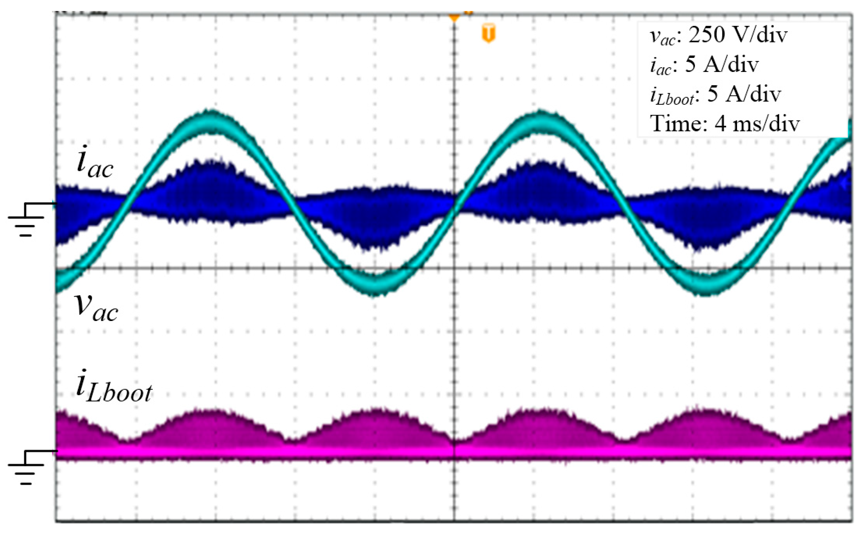
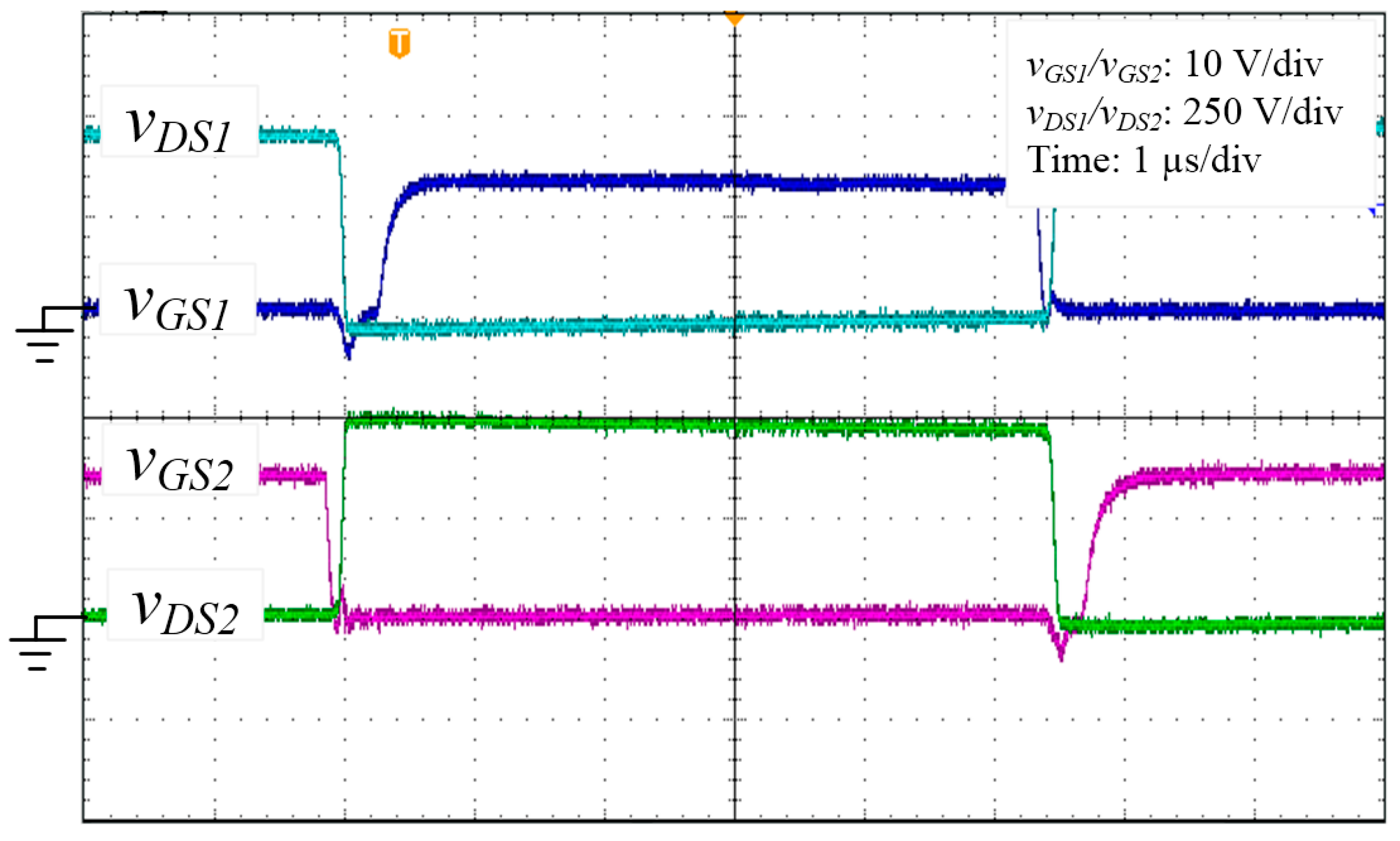
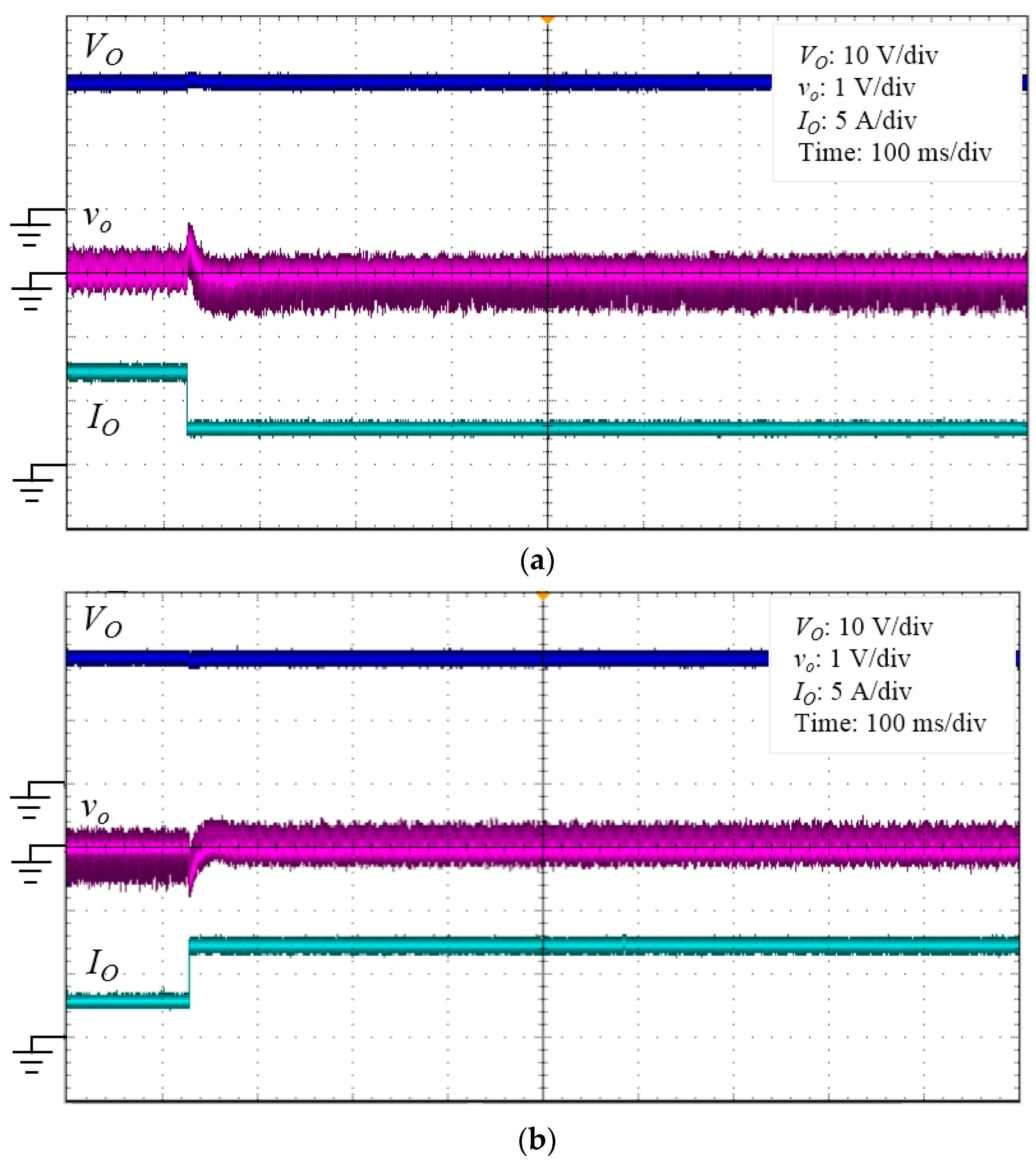
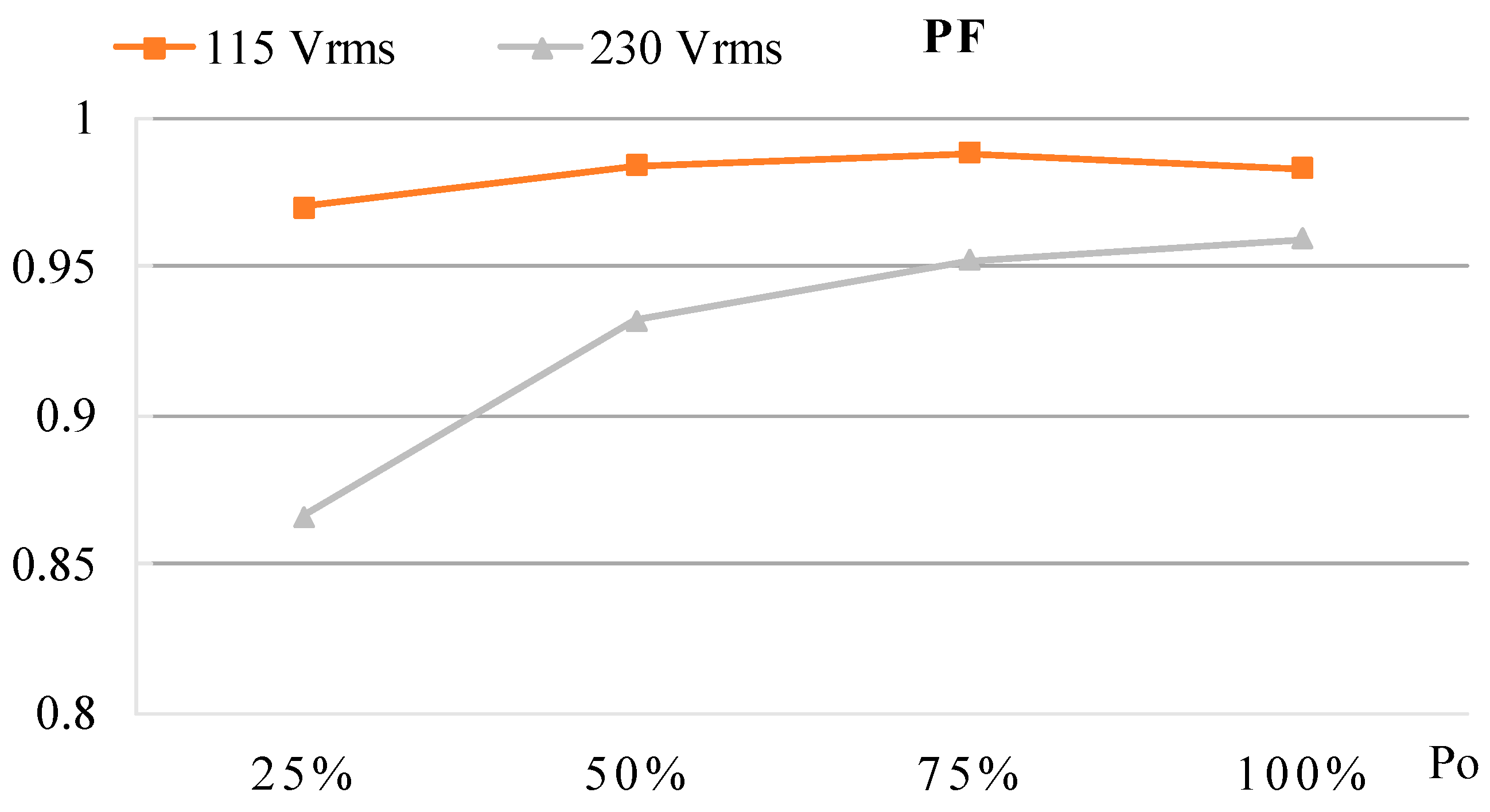
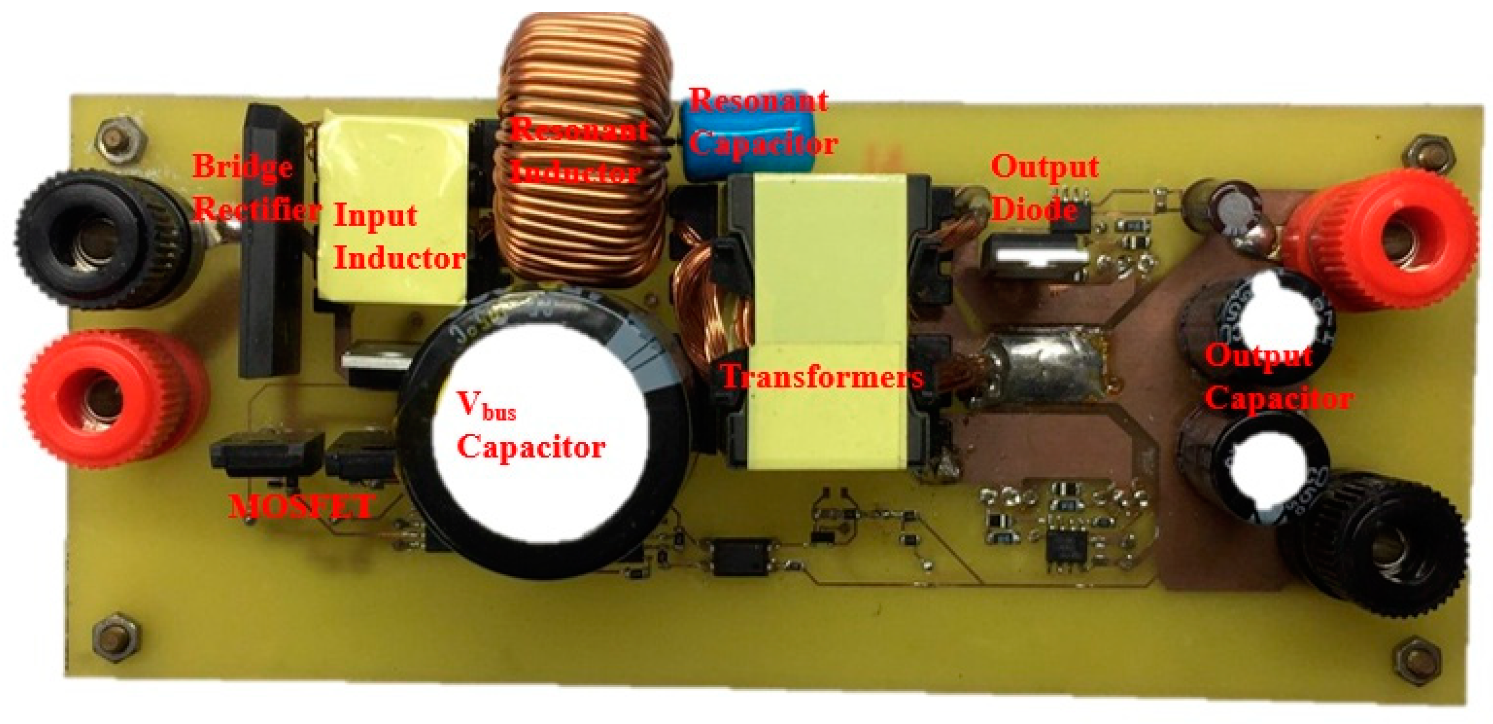
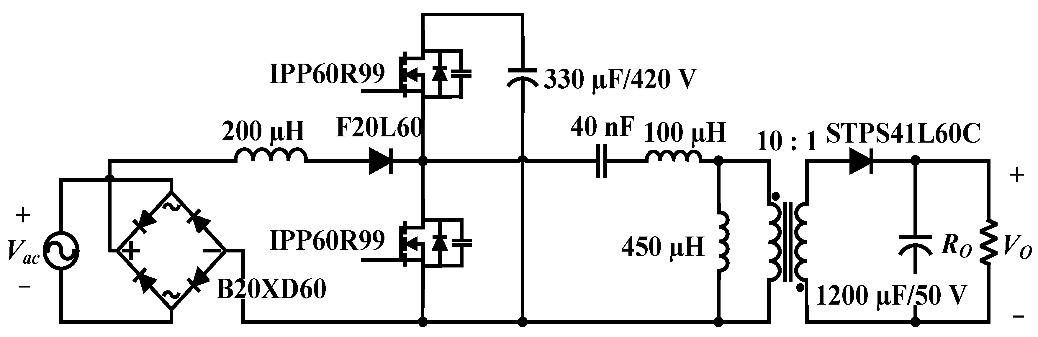
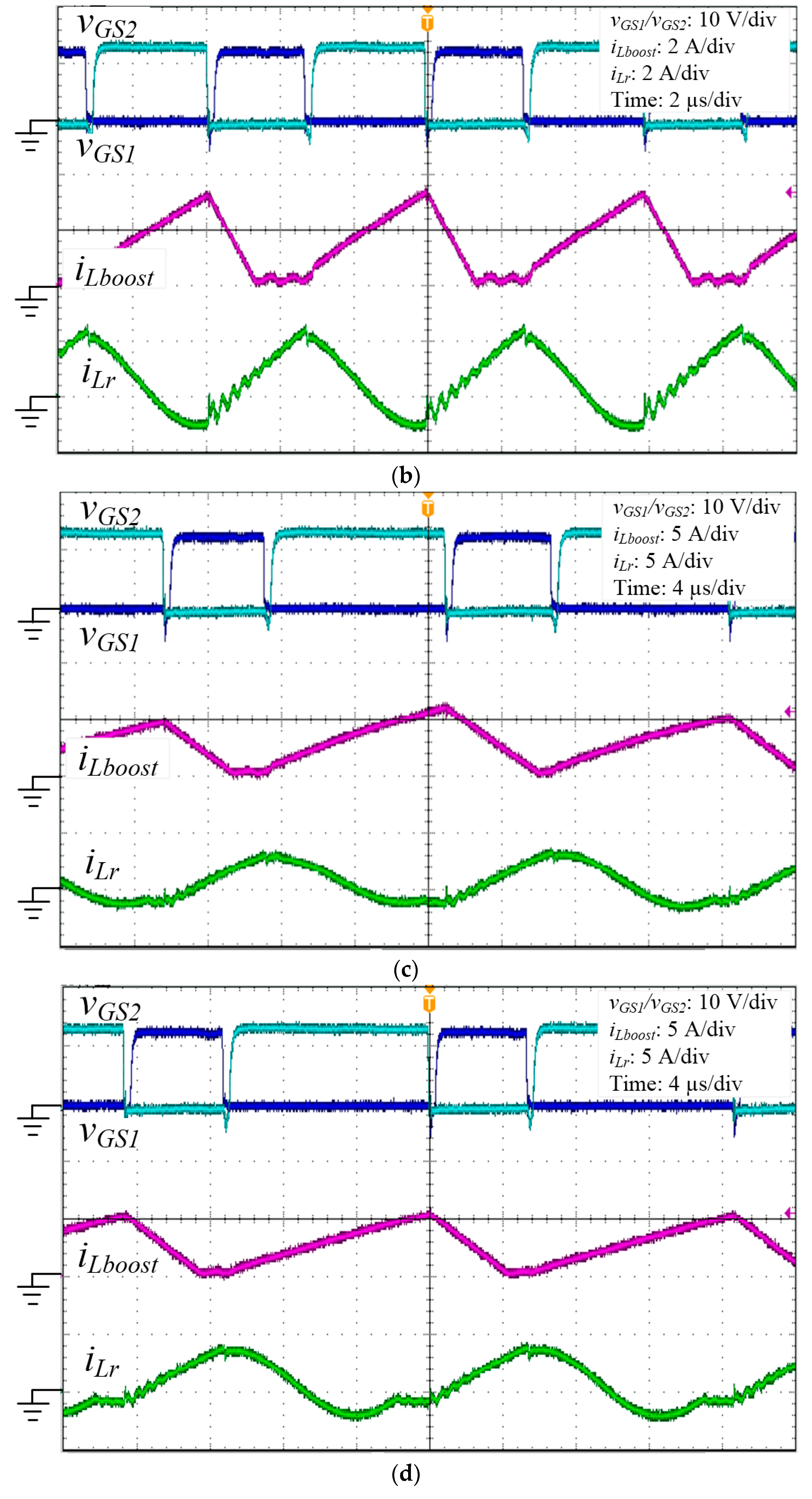
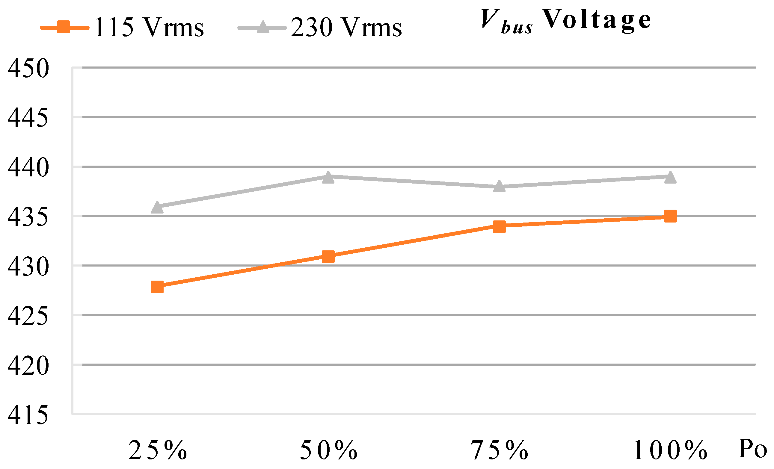
4. Experimental Results

In order to verify the feasibility of the proposed converter, a 120 W prototype converter is built in the laboratory. Figure 5 shows the proposed converter and the experimental parameters are designed in Table 1.
A PQ26/20 TDK core is used for the input inductor. The PQ32/30 core is used for the isolation transformer and the transformer turn ratio is calculated from Equation (26). The magnetizing inductance Lm is designed from Equation (29) at approximately 450 µH. The IPP60R99 MOSFET is used producing output capacitance COSS of about 130 pF at a 430 V drain-to-source voltage, including the output capacitances of Q1 and Q2 it is about 260 pF. Therefore, to ensure ZVS operations, 330 ns dead time was inserted between the Q1 and Q2 gate signals. The resonant frequency fr is placed at about 80 kHz so the resonant capacitor Cr and resonant inductor Lr can be calculated from Equation (32). The output voltage ripple △VO is required to be smaller than 0.95 V. The output capacitor CO is calculated to be greater than 474 µF from Equation (33). Therefore, a 1200 µF output capacitor is used.
Figure 6 shows the experimental results for vGS1, vGS2, iLboost and iLr at different output currents and at VIn,main. Referring to Figure 3, six operation states can be observed in Figure 6. When Q1 is turned on and Q2 is turned off, the iLboost linearly decreases and iLr linearly increases. When Q1 and Q2 are turned off, ZVS operation can be achieved. During the Q1 turned off and Q2 turned on period, the iLboost increases linearly and the resonant inductor Lr and resonant capacitor begin to resonate. On the other hand, Figure 6 also shows that when the output load increases from light load to full load, the duty ratio of Q2 increases from 0.5 to 0.75 for regulated bus voltage Vbus, and the switching frequency decreases from about 125 kHz to 62 kHz for regulated output voltage VO. Figure 7 shows the measured input voltage vac, input current iac and input inductor current iLboost under full load conditions. The input current near sinusoidal waveform and input inductor current are shown operated in DCM so that high power factor can be achieved.
Figure 8 shows the gate-to-source waveforms and drain-to-source voltages for primary switches Q1 and Q2 at the full-load. The waveform shows that VDS1 and VDS2 reach zero levels after Q1 and Q2 are turned on. Therefore, ZVS conduction is achieved so that overall conversion efficiency is increased. The transient output voltage VO during a step load current from 1.6 to 6.3 A and from 6.3 to 1.6 A are shown in Figure 9 when input voltage of 230 Vrms, which shows that VO can still be regulated. Figure 10 depicts the bus voltage variation under 25%, 50%, 75% and 100% load condition and the bus voltage is regulated around 430 V. Figure 11 also depicts the input current power factor. It indicates that the power factor is greater than 0.9 at different load conditions. Figure 12 shows the measured efficiencies of the proposed single stage asymmetrical half-bridge fly-back converter through different outputs. The average efficiency is around 86% above which the rated full load efficiency is about 90%.
Table 2 shows the comparison among the converters proposed in [14,15,17]. Compared with the input voltage range, this presented converter can be operated in universal-voltage, and other converter just can operate in high-line voltage situations. Moreover, this proposed converter has the lowest component cost because it does not need an additional power-device or inductor for a high PF. Figure 13 shows the prototype of the proposed converter.

5. Conclusions

This paper presented a single stage asymmetrical half-bridge fly-back converter with resonant mode. The switches operate simultaneously in the variable-frequency-controller (VFC) and pulse-width-modulation (PWM) control to regulate the bus voltage and output voltage. The operating modes in a complete switching cycle were analyzed and discussed in detail. The key equations were derived and the design procedures formulated. The experimental results on an AC input voltage 90 to 264 Vrms with output 120 W prototype were recorded to verify the theoretical scheme. The measured results show that the power factor is above 0.9, the average efficiency is around 86% and the highest conversion efficiency is about 90%. The proposed single stage asymmetrical half-bridge fly-back converter is especially suitable for low-to-medium power level applications.

Author Contributions

C.-Y.T. designed, simulated the work, and wrote the paper; Y.-C.H. implemented the work and performed the experiment; J.-Y.L. provided all material for implementing the work, supervised the design, circuit simulation, analysis, experiment, and correct the paper.

Funding

This research was funded by Ministry of Science and Technology of Taiwan grant number MOST 106-2221-E-011-095-MY3 and MOST 117-3113-E-007-001-CC2.

Acknowledgments

The authors would like to acknowledge the financial support of the Ministry of Science and Technology of Taiwan through grant number MOST 106-2221-E-011-095-MY3 and MOST 117-3113-E-007-001-CC2.

Conflicts of Interest

The authors declare no conflict of interest.

References

  1. Qian, J.; Lee, F.C. A high-efficiency single-stage single-switch high-power-factor AC/DC converter with universal input. IEEE Trans. Power Electron. 1998, 13, 699–705. [Google Scholar] [CrossRef]
  2. Kang, F.S.; Park, S.J.; Kim, C.U. ZVZCS single-stage PFC AC-to-DC half-bridge converter. IEEE Trans. Ind. Electron. 2002, 49, 206–216. [Google Scholar] [CrossRef]
  3. Zhang, J.; Lee, F.C.; Jovanovic, M.M. An improved CCM single-stage PFC converter with a low frequency auxiliary switch. IEEE Trans. Power Electron. 2003, 18, 44–50. [Google Scholar] [CrossRef]
  4. Ogata, M.; Nishi, T. Graph-theoretical approach to 2-switch DC-DC converter. Int. J. Circuit Theory Appl. 2005, 33, 161–173. [Google Scholar] [CrossRef]
  5. O’Sullivan, D.L.; Egan, M.G.; Willers, M.J. A Family of Single-Stage Resonant AC/DC Converters with PFC. IEEE Trans. Power Electron. 2009, 24, 398–408. [Google Scholar] [CrossRef]
  6. Willers, M.J.; Egan, M.G.; Daly, S.; Murphy, J.M.D. Analysis and design of a practical discontinuous-conduction-mode BIFRED converter. IEEE Trans. Ind. Electron. 1999, 46, 724–733. [Google Scholar] [CrossRef]
  7. Shu, Y.; Lin, B.T. Add active clamping and soft switching to boost flyback single stage isolated power factor corrected power supplies. IEEE Trans. Power Electron. 2011, 26, 3144–3152. [Google Scholar]
  8. Chen, S.Y.; Li, Z.R.; Chen, C.L. Analysis and Design of single stage AC/DC LLC resonant converter. IEEE Trans. Ind. Electron. 2012, 59, 1538–1544. [Google Scholar] [CrossRef]
  9. Luo, S.; Wei, H.; Zhu, G.; Batarseh, I. Several Schemes of Alleviating Bus Voltage Stress in Single Stage Power Factor Correction Converters. In Proceedings of the Power Electronics and Drive Systems Conference, Hong Kong, China, 27–29 July 1999; pp. 921–926. [Google Scholar]
  10. Wu, X.; Yang, J.; Zhang, J.; Xu, M. Design Considerations of Soft-Switched Buck PFC Converter with Constant On-Time (COT) Control. IEEE Trans. Power Electron. 2011, 26, 3144–3152. [Google Scholar] [CrossRef]
  11. Wu, X.; Zhang, J.; Ye, X.; Qian, Z. Analysis and Derivations for a Family ZVS Converter Based on a New Active Clamp ZVS Cell. IEEE Trans. Ind. Electron. 2008, 55, 773–781. [Google Scholar] [CrossRef]
  12. Choi, B.; Lim, W.; Bang, S.; Choi, S. Small-signal analysis and control design of asymmetrical half-bridge DC-DC converters. IEEE Trans. Ind. Electron. 2006, 53, 511–520. [Google Scholar] [CrossRef]
  13. Watson, R.; Hua, G.C.; Lee, F.C. Characterization of an active clamp flyback topology for power factor correction applications. IEEE Trans. Power Electron. 1996, 11, 191–198. [Google Scholar] [CrossRef]
  14. Kwon, J.M.; Choi, W.Y.; Do, H.L.; Kwon, B.H. Single-stage half-bridge converter using a coupled-inductor. IEE Proc. Electr. Power Appl. 2005, 152, 748–756. [Google Scholar] [CrossRef]
  15. Jung, J.H. Feed-Forward Compensator of operating Frequency for APWM HB Flyback Converter. IEEE Trans. Power Electron. 2012, 27, 211–223. [Google Scholar] [CrossRef]
  16. Kim, H.S.; Jung, J.H.; Baek, J.W.; Kim, H.J. Analysis and design of a multioutput converter using a symmetrical PWM half-bridge flyback converter employing a parallel-series transformer. IEEE Trans. Ind. Electron. 2013, 60, 3115–3125. [Google Scholar]
  17. Kim, K.T.; Kwon, J.M.; Lee, H.M.; Kwon, B.H. Single-stage high-power factor half-bridge flyback converter with synchronous rectifier. IET Power Electron. 2014, 7, 1755–4535. [Google Scholar] [CrossRef]
  18. Buso, S.; Spiazzi, G.; Sichirollo, F. Study of the asymmetrical half-bridge flyback converter as an effective line fed solid state lamp driver. IEEE Trans. Ind. Electron. 2014, 61, 6730–6738. [Google Scholar] [CrossRef]
  19. Song, W.; Zhong, Y.; Zhang, H.; Sun, X.; Zhang, Q.; Wang, W. A Study of Z-Source Dual-Bridge Matrix Converter Immune to Abnormal Input Voltage Disturbance and with High Voltage Transfer Ratio. IEEE Trans. Ind. Inf. 2013, 9, 828–838. [Google Scholar] [CrossRef]
  20. Li, H.; Zhou, W.; Zhou, S.; Yi, X. Analysis and Design of High Frequency Asymmetrical Half Bridge Flyback Converter. In Proceedings of the Electrical Machines and Systems International Conference, Wuhan, China, 17–20 October 2008; pp. 1902–1904. [Google Scholar]
  21. Tse, C.K.; Chow, M.H.L. New Single-Stage Power-Factor-Corrected Regulators Operating in Discontinuous Capacitor Voltage Mode. In Proceedings of the 28th IEEE Power Electronics Specialists Conference, Saint Louis, MO, USA, 27–27 June 1997; pp. 371–377. [Google Scholar]
Figure 1. Schematic of the proposed single-stage asymmetrical half-bridge fly-back converter with resonant mode.
Energies 11 01721 g001
Figure 2. Voltage transfer ratio versus normalized switching frequency.
Energies 11 01721 g002
Figure 3. Key waveforms of the proposed single-stage asymmetrical half-bridge fly-back converter with resonant mode.
Energies 11 01721 g003
Figure 4. Operation Modes of the proposed single-stage asymmetrical half-bridge fly-back converter during one switching period: (a) Mode 1; (b) Mode 2; (c) Mode 3; (d) Mode 4; (e) Mode 5; (f) Mode 6.
Energies 11 01721 g004aEnergies 11 01721 g004b
Figure 5. Implementation of the proposed single-stage asymmetrical half-bridge fly-back converter with resonant mode.
Energies 11 01721 g005
Figure 6. Waveforms for vGS1, vGS2, iLboost and iLr at different load current: (a) 1.6 A; (b) 3.2 A; (c) 4.7 A; (d) 6.3 A.
Energies 11 01721 g006aEnergies 11 01721 g006b
Figure 7. Waveforms for vac, iac and iLboost at vac = 230 Vrms.
Energies 11 01721 g007
Figure 8. Zero-voltage turn-on switching for Q1 and Q2.
Energies 11 01721 g008
Figure 9. Load transient response under different loads: (a) 20% to 100%; (b) 100% to 20%.
Energies 11 01721 g009
Figure 10. Vbus voltage variation curve for 115 Vrms and 230 Vrms.
Energies 11 01721 g010
Figure 11. PF curve for 115 Vrms and 230 Vrms.
Energies 11 01721 g011
Figure 12. Efficiency curve for 115 Vrms and 230 Vrms.
Energies 11 01721 g012
Figure 13. The prototype of the proposed converter.
Energies 11 01721 g013
Table 1. Experimental parameters of the proposed converter.
ParametersValue
Input ac voltage range:85–264 Vrms
Output voltage:VO = 19 V
Output voltage ripple:VO = 0.95 V
Intermediate bus voltage:Vbus = 420 V
Maximum output current:IO = 6.32 A
Input inductor:Lboost = 200 µH
Magnetizing inductance:Lm = 450 µH
Turns ratio:n = Np/Ns = 3T
Resonant inductor:Lr = 100 µH
Maximum duty cycle:Dmax = 0.75
Resonant capacitors:Cr = 40 nF
Switching frequency:fs = 60–150 kHz
Output capacitor:CO = 1200 µF
Table 2. Comparison to the other published methods.
Proposed Converter2005 [14]2012 [15]2014 [17]
Input Voltage90–264 Vrms180–265 Vrms180–270 Vrms180–265 Vrms
Output Voltage19 V24 V24 V24 V
Switching Frequency60–150 kHz100 kHz99–119 kHz100 kHz
Efficiency90%91%91.5%92%
Power Factor98%99%None99%
ZVS/ZCSYesYesYesYes
Control Techniques for power factorVCF and PWMCoupled InductorFrequency CompensatorPWM
CostLowHighMiddleHigh

