Article

Sliding-Mode Control of Distributed Maximum Power Point Tracking Converters Featuring Overvoltage Protection

by
Carlos Andres Ramos-Paja
1,
Daniel Gonzalez Montoya
2,* and
Juan David Bastidas-Rodriguez
3
1
Departamento de Energia Eléctrica y Automática, Universidad Nacional de Colombia, Carrera 80 No 65-223—Facultad de Minas, Medellín 050041, Colombia
2
Departamento de Electrónica y Telecomunicaciones, Instituto Tecnológico Metropolitano, Carrera 31 No 54-10, Medellín 050013, Colombia
3
Escuela de Ingenierías, Eléctrica, Electrónica y de Telecomunicaciones, Universidad Industrial de Santander, Bucaramanga 68002, Colombia
*
Author to whom correspondence should be addressed.
Energies 2018, 11(9), 2220; https://doi.org/10.3390/en11092220
Submission received: 10 July 2018 / Revised: 14 August 2018 / Accepted: 15 August 2018 / Published: 24 August 2018
(This article belongs to the Special Issue Control and Nonlinear Dynamics on Energy Conversion Systems)

Abstract

:
In Photovoltaic (PV) systems with Distributed Maximum Power Point Tracking (DMPPT) architecture each panel is connected to a DC/DC converter, whose outputs are connected in series to feed a grid-connected inverter. The series-connection forces the output voltage of those converters to be proportional to the converter’ output power; therefore, under mismatched conditions, the output voltage of a highly-irradiated converter may exceed the rating (safe) value, causing an overvoltage condition that could damage the converter. This paper proposes a sliding-mode controller (SMC) acting on each converter to regulate both the input and output voltages, hence avoiding the overvoltage condition under partial shading. The proposed control strategy has two operation modes: maximum power point tracking (MPPT) and Protection. In MPPT mode the SMC imposes to the PV panel the voltage reference defined by an MPPT technique. The Protection mode is activated when the output voltage reaches the safety limit, and the SMC regulates the converter’ output voltage to avoid overvoltage condition. The SMC has a bilinear sliding surface designed to provide a soft transition between both MPPT and Protection modes. The SMC analysis, parameters design and implementation are presented in detail. Moreover, simulation and experimental results illustrate the performance and applicability of the proposed solution.

1. Introduction

The continuous growing of Photovoltaic (PV) systems in the last years has consolidated PV technology as one of the most important renewable energy sources. Only in 2017 approximately 96 GW were installed, i.e., 29% more with respect to 2016, reaching a global installed PV capacity of 402.5 GW , approximately [1].
Most of the PV installed capacity corresponds to grid-connected PV systems (GCPVS) aimed at supplying electricity demand in different applications. In general, a GCPVS is composed by a PV generator, one or more DC/DC power converters, an inverter and a control system [2]. The PV generator transforms the sunlight into electric power, which depend on the environmental conditions (irradiance and temperature) and the operation point. The DC/DC converters allows the modification of the PV generator operation point and the DC/AC converter delivers the electrical power to the grid. The control system can be divided into two main parts: maximum power point tracking (MPPT) and inverter control. On the one hand, the MPPT uses the DC/DC power converters to find and track the PV generator operation point where it delivers the maximum power (MPP). On the other hand, the inverter control has two main tasks, the first one is to synchronize the AC voltage with the grid, and the second one is to inject the AC current to the grid, which is proportional to the power delivered by the PV generator and the DC/DC converters [3,4].
The inverter control is particularly important in a GCPVS because the stability and the power quality injected to the grid depend on it [2,3,4]. For this controller, the PV generator, the DC/DC converters and the MPPT are represented by a voltage [2] or a current [3,4] source, which feeds a link capacitor to form a DC bus. The DC voltage is converted to AC with a set of switches, and a filter eliminates the high frequency components [2]. The voltage-source two-level inverters with L, LC or LCL filters are widely used in commercially available inverters [2,5] and the inverter controller is usually a cascaded control where inner loop regulates voltage and the outer loop controls the current injected to the grid and keeps the DC bus voltage around its reference value [2]. Nonetheless, other authors propose cascaded controller where the inner loop regulates the current injected to the grid [3,4,6,7] and the current references are generated from a Droop controller [7], active and reactive power references [6] or form the maximum power provided by the PV source and the reactive power demanded by the load [3,4]. Moreover, some papers propose linear current controllers [6], while other papers combine linear regulators with state feedback [3,7] or Lyapunov-based [4] controllers to regulate the current injected to the grid.
Notwithstanding the important role of the inverter controller in a GCPVS, the maximum power delivered by the PV generator does not depend on this controller, since the MPPT is in charge of finding and tracking the MPP of the PV generator for different irradiance and temperature conditions. When all the the PV panels in a generator are operating under the same irradiance and temperature conditions (i.e., homogeneous conditions), there is a single MPP in the power vs. voltage (P-V) curve of the generator. However, GCPVS in urban environments (i.e., homes, buildings, companies, etc.) are surrounded by different objects, which may produce partial shadings over the PV array, which forces the PV panels of the array to operate under different (mismatched) irradiance and temperature conditions. Moreover, mismatching conditions may also be produced by the aging, soiling, early degradation and manufacturing tolerances in the PV panels [8].
When a PV generator is operating under mismatching conditions, the power produced is significantly reduced [9,10]; therefore, it is important to mitigate their effects. In general, it is possible to find three different architectures to mitigate the adverse effects of the mismatching conditions in PV installations: centralized systems (CMPPT), distributed systems (DMPPT), and reconfiguration systems [11]. However, CMPPT and DMPPT architectures are the most widely used architectures in urban applications; hence they are briefly discussed below.
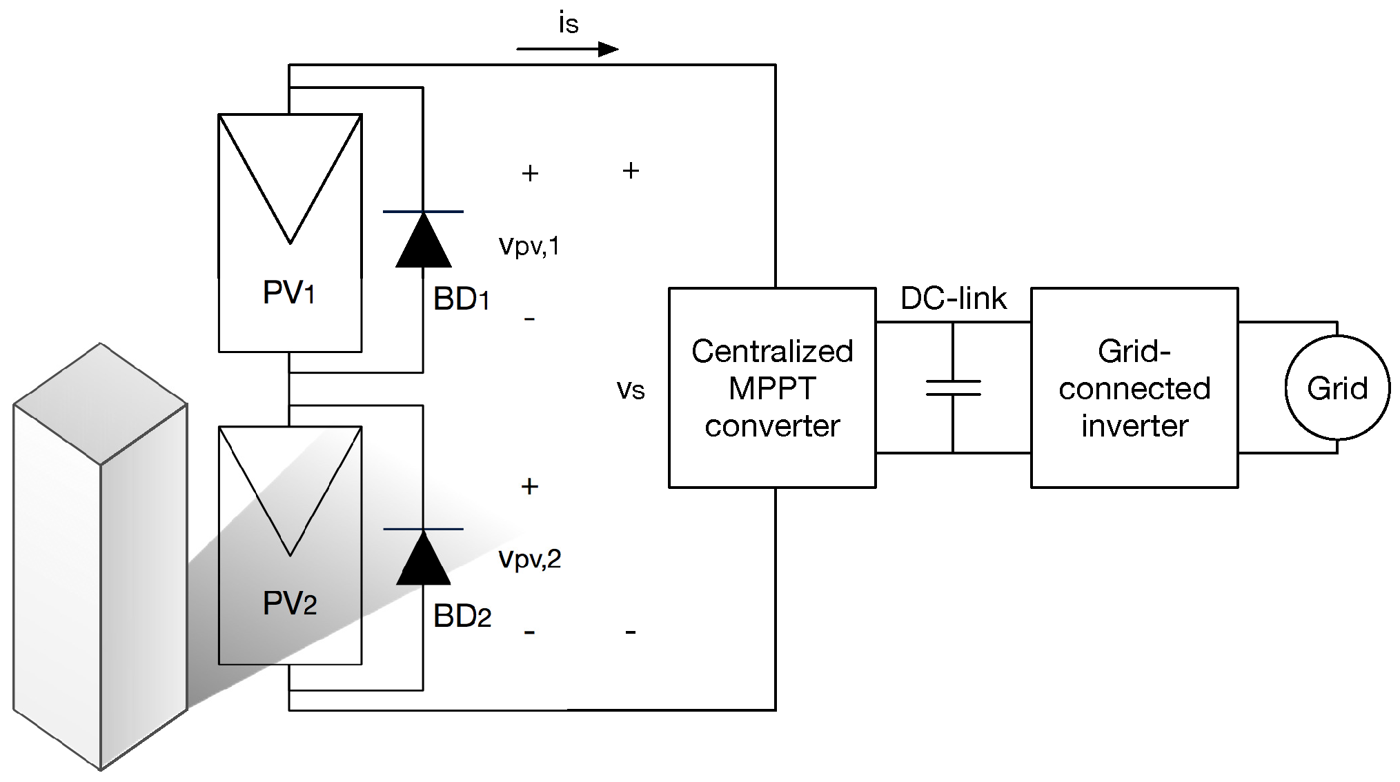
In CMPPT systems, depicted in Figure 1, the complete PV array is connected to a single DC/DC power converter, whose output is connected to the grid through an inverter. The DC/DC converter modifies the operation voltage of the PV array, in order to track the MPP through the MPPT. Under mismatching conditions, the maximum current (i.e., the short-circuit current) produced by a shaded PV panel is less than the short-circuit current of the unshaded panels; hence, when the array current is greater than the short-circuit current of the shaded panel, the excess of current flows through the bypass diode (BD) connected in antiparallel to the panel (see Figure 1). As consequence, for a particular shading profile over the PV panels and a particular array current, some BDs are active and the rest are inactive. This activation and deactivation of the bypass diode produce multiple MPPs in the array P-V curve, which means that there are local MPPs and one global MPP (GMPP) [12].
In general, MPPT techniques for CMPPT architectures are complex [11,12] because they should be able to track the global MPP of the PV array in any condition. Moreover, mismatching conditions continuously change along the day and year due to the sun trajectories in the sky, and also due to the changes in the surrounding objects. As consequence, the number of MPPs and the location of the global MPP continuously change in the P-V curve of a PV array. CMPPT techniques can be classified into three main groups [13]: conventional techniques, soft computing techniques and other techniques. The first group includes techniques based on Perturb & Observe (P&O), incremental conductance and hill climbing, as well as other GMPP search techniques and adaptive MPPTs. Soft computing techniques uses artificial intelligence methods to find the GMPP, like evolutionary algorithm, genetic programming, fuzzy system, among others. The last group includes methods like Fibonacci search, direct search, segmentation search, and others to locate the GMPP.
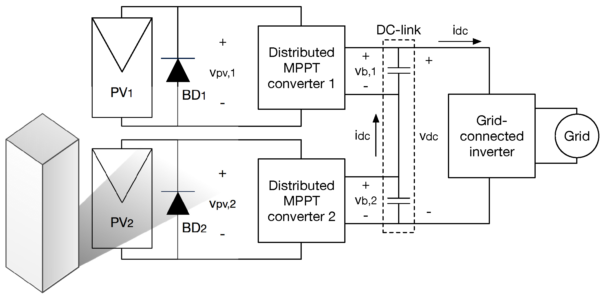
In DMPPT architectures the PV array is divided into smaller arrays, or sub-arrays, to reduce the number of MPPs in each sub-array. Then, each sub-array is connected to a DC/DC power converter, which has an MPPT technique much more simple than the ones used in CMPPT systems [11,14,15]. The double stage DMPPT system, presented in Figure 2, is one of the most widely adopted architectures in literature [11,14,15], where each panel is connected to a DC/DC converter to form a DMPPT unit (DMPPT-U) and all DMPPT-Us are connected in series to feed an inverter. Boost converters are widely used as DC/DC converter in double stage DMPPT system, while other approaches uses buck, buck-boost or more complex converters to improve the voltage gain or the efficiency [13,15].
The main advantage of the double stage DMPPT systems is that each PV panel can operate at its MPP even under mismatching conditions [15]. Moreover, no communication is required among the DMPPT-Us or with the inverter, and the the dynamics of the DMPPT-Us are decoupled from the dynamics of the GCPVS inverter, due to the high capacitance in the DC link that forms the DC bus [15]. However, one of the main limitations of double stage DMPPT systems is that the output voltage of each DMPPT-U is proportional to its output power; therefore, under mismatching conditions, the output voltage of a DMPPT-U with a highly irradiated PV panel may exceed the maximum voltage of the DMPPT-U output capacitor and the maximum open-circuit voltage of the switching devices. Such a condition is denominated overvoltage and must be avoided to protect the DC/DC converter [16,17,18]. Although overvoltage condition is important to assure a secure operation of the DMPPT-Us, it is not discussed in some papers devoted to analyzing double stage DMPPT systems, like [19,20], nor in review papers about MPPTs for PV generators under mismatching conditions [13,15,21,22].
In general, overvoltage can be faced by two main approaches. The first one is to design the DMPPT-U with an output capacitor and switching devices able to endure voltages that may be close to the DC bus voltage in the link with the inverter [18]. Nevertheless, this solution increases the size and cost of each DMPPT-U, hence, this effect is multiplied by the number of DMPPT-Us in the PV system. The second approach is to monitor the DMPPT-U output voltage and if it is greater than a reference value, the control objective must be changed to regulate the DMPPT-U output voltage under its maximum value. This operating mode is denominated Protection mode.
Therefore, the DMPPT-U control strategy must consider two basic operation modes: MPPT and Protection. In MPPT mode the control objective is to extract the maximum power from the PV generator, while monitors the output voltage of the DMPPT-U. If such a voltage surpasses a reference value, then MPPT mode is disabled and Protection mode is activated to keep the DMPPT-U output voltage below its maximum value. Although in literature there is a significant number of control systems for double stage DMPPTs, as shown in different review papers [13,14,15], after an exhaustive review the authors have found just a few control systems that consider the overvoltage problem and implement MPPT and Protection modes [16,23,24,25,26,27,28,29,30]. That is why, the literature review in this paper is focused on these references.
In [23,24,25] the authors propose centralized strategies to perform the MPPT and to avoid the condition v b > V m a x on DMPPT-Us implemented with Boost converters, where v b and V m a x are the output voltage of the DC/DC converter and its maximum value, respectively. In [23,24] the authors propose to monitor v b of each DMPPT-U, if there is at least one DMPPT-U with v b > V m a x , then the input voltage of the inverter ( v d c ) is reduced. Moreover, when v d c is reduced below 80 % of its nominal value, the DMPPT-Us with v b > V m a x change their operating mode from MPPT to v b regulation. Nevertheless, the authors use linear controllers for v p v and v b , which no not guarantee the DMPPT-U stability in the full operation range. Additionally, the paper does not provide information about the implementation of the v b controller and it does not discuss how to perform the transition between MPPT and Protection mode (and viceversa) or the stability issues of those transitions. Finally, the paper does not provide guidelines or a design procedure of the proposed control system.
Another centralized control strategy for a DMPPT system, based on Particle-Swarm Optimization (PSO), is proposed in [25]. The objective of the control strategy is to find the values of v p v of each DMPPT-U that maximizes the output power of the whole system. However, the constraints of the PSO algorithm include the condition v b < V m a x for each DMPPT-U. Therefore, the proposed control system is able to track the MPPT in each DMPPT-U avoiding the overvoltage condition. Although the authors provide some considerations to set the PSO parameters, they not explain how regulate the PV panel voltage with the power converters and they do not analyze the stability of the DMPPT-Us. Moreover, the authors do not provide information for the implementation of the proposed control system because they implemented it on a dSpace control board. It is worth noting that the centralized strategies proposed in [23,24,25] require additional hardware to implement the centralized controllers and monitoring systems, hence these solutions require high calculation burden compared with other DMPPT-U control approaches like [16,26,27,28,29].
The authors in [16,26] consider DMPPT-Us implemented with Boost converters and propose to limit the duty-cycle (d) of each DMPPT-U to avoid the condition v b > V m a x . The limit of d is defined as d < 1 v p v / v b , where, v p v is the PV panel voltage [16,26]. Nevertheless, the DMPPT-U control operates in open-loop during the saturation of d, which may lead to the instability of the DMPPT-U controller. Additionally, the papers do not provide a clear explanation about how to define the duty cycle limit, since the voltage v p v of a DMPPT-U varies with the irradiance and temperature conditions as well as the mismatching profile over the PV panels. Finally, the authors in [16] focus on the analysis of double stage DMPPT systems implemented with boost converters, but they do not provide a design procedure for the DMPPT-U control in MPPT mode.
In [27,28,29] the authors propose two different control strategies for each DMPPT-U, one for MPPT mode and another for Protection mode, where the trigger for the Protection mode is the condition v b > V m a x . On the one hand, the strategy presented in [27] for Protection mode is to adopt a P&O strategy, i.e., perturb v p v and observe v b in order to fulfill the condition v b < V m a x . On the other hand, in [28,29] two PI-type regulators are proposed for each DMPPT-U: one for v p v in MPPT mode and another for v b in Protection mode. The reference of v b and v p v regulators are V m a x and the MPPT reference, respectively. The voltage regulators presented in [27,28,29] are linear-based, with fixed parameters, and designed with a linearized model in a single operation point of the DMPP-U; therefore, they cannot guarantee a consistent dynamic performance and stability of the DMPPT-U in the entire operation range. Moreover, the authors in [27,28,29] do not provide a design procedure of the proposed controllers and only [28] provide relevant information for the controller implementation.
A Sliding-Mode Controller (SMC) designed to regulate v p v and v b on a Boost-based DMPPT-U is proposed in [30]. The sliding surface ( Ψ ) has three terms: Ψ = i L k p v · v p v v m p p t · 1 O V k b v b V m a x · O V , where i L is the inductor current of the Boost converter, v m p p t is the v p v reference provided by the MPPT algorithm, O V is a binary value assuming O V = 1 when v b > V m a x and O V = 0 when v b < V m a x , and the constants k p v and k b are SMC parameters. During MPPT mode the first and second terms of Ψ are active to regulate v p v according to the MPPT algorithm; while during Protection mode the first and third terms of Ψ are active to regulate v b = V m a x . The main advantage of the SMC proposed in [30] is the capability to guarantee the global stability of the DMPPT-U in the entire operation range. Nonetheless, that paper does not analyze the dynamic restrictions of the SMC reference in MPPT to guarantee the DMPPT-U stability; additionally, the paper does not provide a design procedure for the SMC parameters ( k p v and k b ) and the sliding surface does not include integral terms, which introduces steady-state error in the regulation of v p v and v b . Finally, the authors do not provide information for the real implementation and the proposed control system is validated by simulation results only.
This paper introduces a control strategy with MPPT and Protection modes for DMPPT-Us implemented with boos converters, where the regulation of v p v , in MPPT mode, and v b , in Protection mode, is performed by a single SMC. In MPPT mode v p v reference is provided by a P&O algorithm and v b is monitored to verify if its value is less than a safe limit named V m a x . If v b V m a x , Protection mode is activated and v b is regulated to V m a x by the SMC. During Protection mode v b is monitored to verify the condition v b < V m a x , if so, MPPT mode is activated. The proposed SMC has the same structure of the SMC introduced in [30] to adapt the SMC switching function with the operation mode. However, the proposed SMC introduces two integral terms to guarantee null steady-state error in the regulation of v p v and v b ; moreover, the paper analyzes the dynamic restrictions in the P&O references to ensure the stability of the DMPPT-U in the entire operation range. The design procedure of the proposed SMC parameters is analyzed in detail as well as its implementation using embedded systems and analog circuits.
There are three main contributions of this paper. The first one is a single SMC that guarantees global stability and null steady-state error of the DMPPT-Us in the entire operation range of MPPT and Protection modes. The second contribution is a detailed design procedure of the proposed SMC parameters and the definition of the dynamic limits of P&O references that guarantee the global stability. Finally, the last contribution is the detailed description of the SMC implementation that helps the reader to reproduce the results.
The rest of the paper is organized as follows: Section 2 explains the effects of the mismatching conditions on a DMPPT system; Section 3 introduces the model of the DMPPT-U and the structure of the proposed SMC. Section 4 and Section 5 provide the analysis and parameters design of the proposed SMC in both MPPT and Protection modes. Then, Section 6 describes the implementation of the proposed SMC, and Section 7 and Section 8 present both the simulation and experimental results, respectively. Finally, the conclusions given in Section 9 close the paper.

2. Mismatched Conditions and DMPPT

In a CMPPT system operating under mismatching conditions, there are some panels subjected to a reduced irradiance due to, for example, the shadows produced by surrounding objects (see Figure 1); hence, the maximum current (short-circuit current) of those panels is lower than the short-circuit current of the non-shaded panels. Moreover, when the string current is lower than the short-circuit current of the shaded PV panel, the protection diode connected in antiparallel, i.e., bypass diode (BD), is reverse biased (inactive) and both panels contribute to the string voltage. However, when the string current is higher than the short-circuit current of the shaded panel, the BD of such panel is forward biased (active) to allow the flow of the difference between the string current and the short-circuit current of the shaded panel.
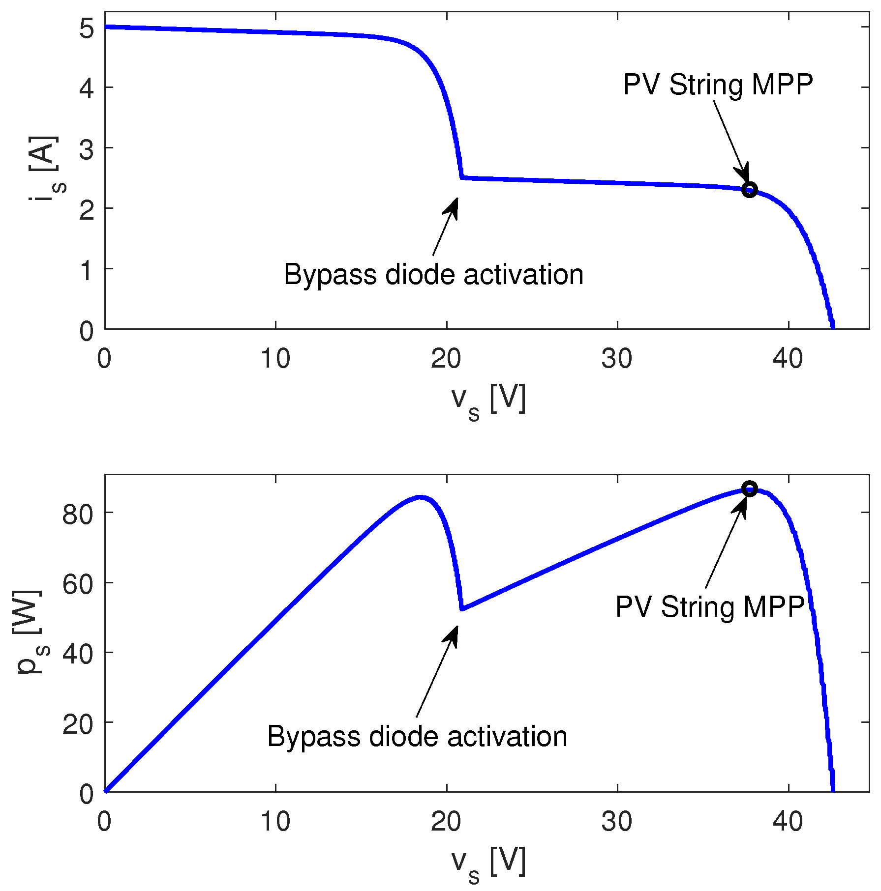
The Current vs. Voltage (I-V) and P-V curves of a PV array, composed by two PV panels, is simulated to illustrate the mismatching effects on the CMPPT system presented in Figure 1. For the simulation, the non-shaded ( PV 1 ) and shaded ( PV 2 ) panels irradiances are S 1 = 1000 W / m 2 and S 2 = 500 W / m 2 , respectively. The panels are represented by using the single-diode model expression given in Equation (1) [31], where v p v and i p v are the current and voltage of the panel, i p h is the photovoltaic current, A is the inverse saturation current, R s is the series resistance and R h is the parallel resistance. B is defined as B = N s · η · k · T / q where N s is the number of cells in the panel, η is the ideality factor, k is the Boltzmann constant, q is the electron charge, and T is panel temperature in K. The parameters used for the simulations are calculated using the equations presented in [32]: A = 154.15 μ A , B = 1.1088 V 1 , R s = 0.0045 Ω and R h = 109.405 Ω .
i p v = i p h A · exp v p v + R s · i p v B 1 v p v + R s · i p v R h
The BD activation of the shaded PV panel in Figure 1 produces an inflection point in the I-V curve, which in turns produces two MPPs in the P-V curve as it is shown in Figure 3. Therefore, the maximum power produced by the CMPPT system ( 86.52 W ) is less than 123.28 W , which is the sum of the maximum power that can be produced by both PV 1 ( 84.25 W ) and PV 2 ( 39.03 W ).
In a double stage DMPPT system, each panel is connected to a DC/DC converter to form a DMPPT unit (DMPPT-U), and the converters’ outputs are connected in series to obtain the input voltage of an inverter, as reported in Figure 2. The boost converter is a widely used topology to implement the DMMPT-Us [11,14,16,23,24,25,26,27,29,30], since it is necessary to step-up the PV panel voltage to match the inverter input voltage. Moreover, the boost structure is simple and the stress voltages of both output capacitor and switch are smaller in comparison with other step-up topologies [33]. Furthermore, the series connection of the DMPPT-U outputs impose low boosting factors to the boost converters, which enables those topologies to operate in a high efficiency condition.
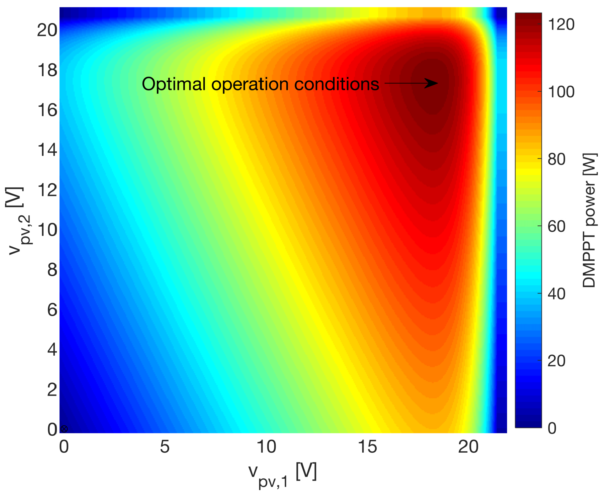
To illustrate the theoretical power extraction provided by a double stage DMPPT solution, the system of Figure 2 is simulated considering the same mismatching conditions adopted for the CMPPT solution: S 1 = 1000 W / m 2 and S 2 = 500 W / m 2 . The simulation results are presented in Figure 4. In this case, both PV panels are able to operate at any voltage, hence the maximum power achievable in each panel is extracted. Therefore, the theoretical optimal operation conditions v p v , 1 = 18.43 V , v p v , 2 = 17.64 V correspond to the MPP conditions in each panel as reported in Figure 4, in which PV 1 has a maximum power of 84.25 W and PV 2 has a maximum power of 39.03 W , hence the maximum power provided by the DMMPT system is 123.28 W ; this is considering loss-less converters.
However, from Figure 2 it is observed that the DC-link is formed by the output capacitors of the DMPPT converters, which are connected in series. Therefore, the DC-link voltage v d c is equal to the sum of the output capacitors voltages v b , 1 and v b , 2 . For a general system, with N DMPPT converters associated to N PV panels, such a voltage condition is expressed in Equation (2):
v b , 1 + v b , 2 + + v b , i + + v b , N = j = 1 N v b , j = v d c
Moreover, the series connection of the output capacitors imposes the same current at the output of the DMPPT converters. Therefore, the power delivered to the DC-link p d c , which is transferred to the grid-connected inverter, is equal to the sum of the power delivered by each converter, p b , 1 and p b , 2 . In the general system formed by N converters, the following expression holds:
p b , 1 + p b , 2 + + p b , i + + p b , N = j = 1 N p b , j = p d c
Finally, the voltage imposed to the i-th output capacitor is obtained from Equations (2) and (3) as follows:
v b , i = v d c · p b , i j = 1 N p b , j
That expression put into evidence that the voltage imposed to any of the output capacitors depends on the power delivered by all the DMPPT converters. Moreover, grid-connected inverters, like the one described in Figure 2, regulate the DC-link voltage at its input terminals to ensure a correct and safe operation [34]. In light of the previous operation conditions, Equations (2) and (4) reveal that the DC-link voltage v d c , imposed by the inverter, is distributed into the output capacitor voltages v b , i proportionally to the power delivered by the associated PV panel p p v , i with respect to the total power delivered by all the PV sources. Hence, the converter providing the higher power will exhibit the higher output voltage, which could lead to over-voltage conditions.
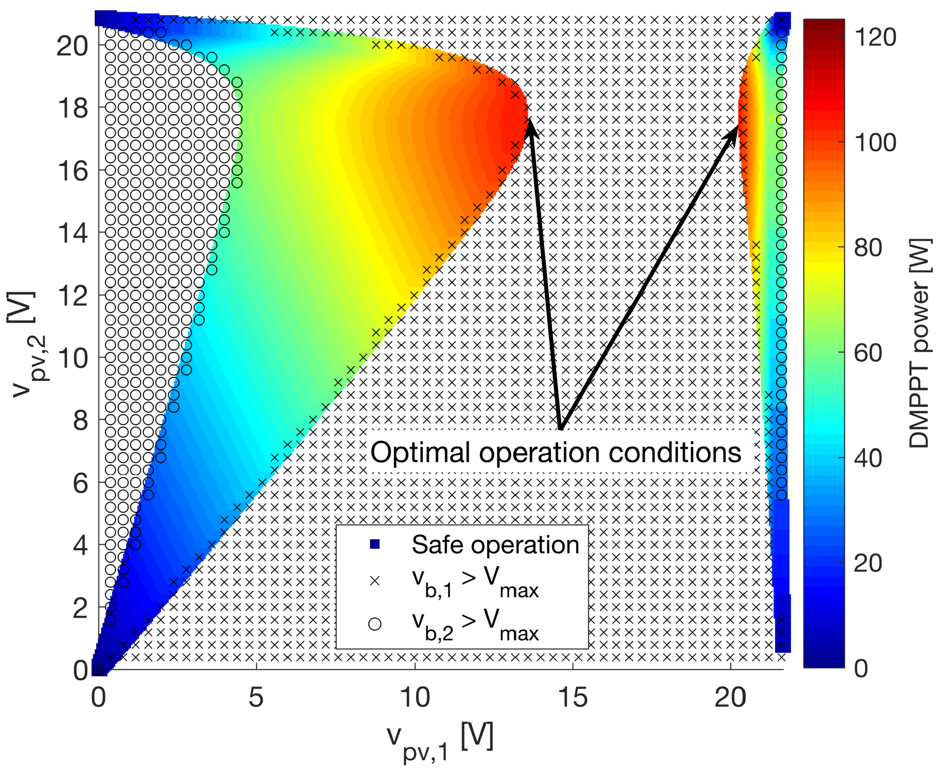
Considering the DMPPT system of Figure 2 with a DC-link voltage imposed by the inverter equal to v d c = 80 V , and output capacitors with maximum voltage rating equal to V m a x = 50 V , the DMPPT system operates safely if both PV panels produce the same power since v b , 1 = v b , 2 = 40 V . However, in the mismatched conditions considered ( S 1 = 1000 W / m 2 and S 2 = 500 W / m 2 ), the DMPPT system is subjected to overvoltage conditions as it is reported in Figure 5: at the theoretical optimal operation conditions v p v , 1 = 18.43 V , v p v , 2 = 17.64 V the output voltage of the first converter is 54.67 V , which is higher than the rating voltage V m a x producing an overvoltage condition that could damage the converter. Figure 5 shows the conditions for safe operation, overvoltage in the first converter ( v b , 1 > V m a x ) and overvoltage in the second converter ( v b , 2 > V m a x ).
The simulation puts into evidence that new optimal operation condition appear due to the overvoltage conditions. In this example, the first optimal operation points of the PV panels are v p v , 2 = 17.64 V (MPP voltage) and v p v , 1 = 13.33 V (no MPP voltage), while the second optimal operation point is v p v , 2 = 17.64 V (MPP voltage) and v p v , 1 = 20.39 V (no MPP voltage). This result is analyzed as follows: the first PV panel must be driven far enough from the MPP condition so that the power provided to the DC-link by the associated converter is, at most, 62.5 % of the total power. That percentage is calculated from Equation (4) replacing the output voltage by the rating voltage V m a x and using the values of the DC-link voltage v d c and the total power delivered to the DC-link as follows:
max p b , i = V m a x · j = 1 N p b , j v d c
Equation (5) shows that, in the cases when the theoretical optimal operation conditions are out of the safe voltages, the new optimal operation voltages are located at the frontier of the safe conditions, which ensures the maximum power extraction from the PV panel associated to the converter near the overvoltage condition. This analysis is confirmed by the simulation results presented in Figure 5.
Therefore, to ensure the maximum power extraction for any irradiance and mismatching profile, the DMPPT converters must be operated in two different modes:
  • MPPT mode: when the output capacitor voltage v b , i is under the safe (rating) limit, the converter must be controlled to track the MPP condition.
  • Protection mode: when the output capacitor voltage v b , i reaches the safe limit, the converter must be controlled to set v b , i at the maximum safe value V m a x .
The following sections propose a control system, based on the sliding-mode theory, to impose the previous behavior to the DMPPT converters.

3. Converter Model and Structure of the Control System

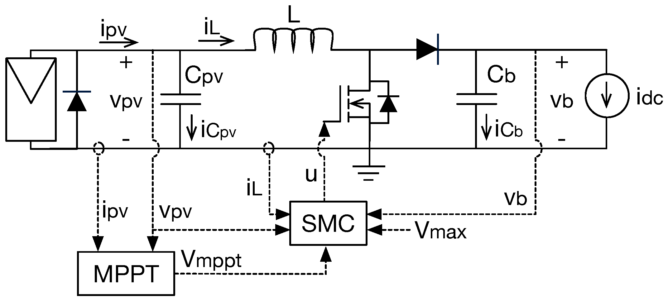
As discussed before, boost converters are widely used in DMPPT systems; hence, this paper considers a DMPPT-U system implemented with a boost converter. The electrical model of the adopted DMPPT converter is presented in Figure 6, which includes the MPPT algorithm that provides the reference for the SMC. Moreover, a current source is used to model the current i d c imposed by the inverter to regulate the DC-link voltage.
The differential equations describing the dynamic behavior of the DMMPT converter are given in Equations (6)–(8), in which u represents the binary signal that defines the MOSFET and diode states: u = 1 for MOSFET on and diode off; u = 0 for MOSFET off and diode on.
d v p v d t = i p v i L C p v
d v b d t = i L · 1 u i d c C b
d i L d t = v p v v b · 1 u L
Sliding-mode controllers are widely used to regulate DC/DC converters because they provide stability and satisfactory dynamic performance in the entire current and voltage operation ranges [35,36]. Furthermore, SMCs also provide robustness against parametric and non-parametric uncertainties [37]. In particular, in PV systems implemented with boost converters, SMCs have been adopted to improve the dynamic performance of the DC/DC converter in CMPPT systems [37,38] and to regulate the input and output voltages of a DMPPT-U operating in both MPPT and Protection modes [30]. Therefore, this paper adopts that type of controllers.
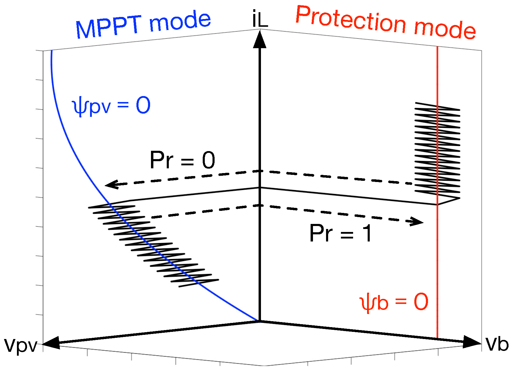
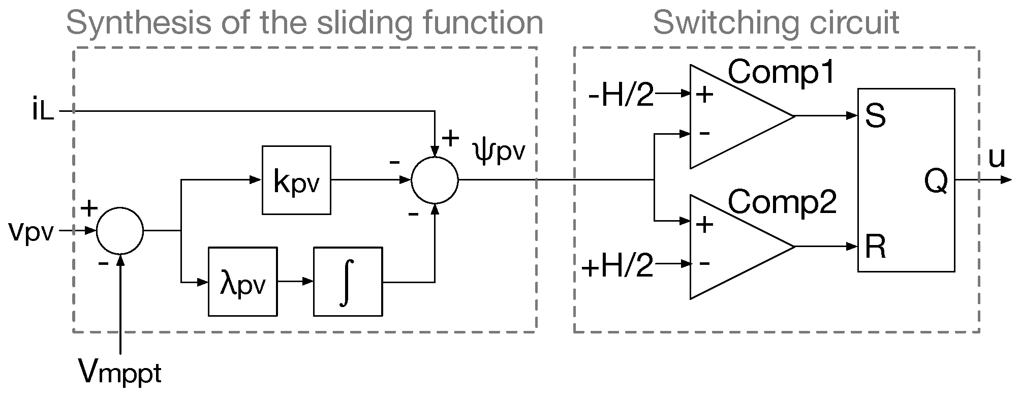
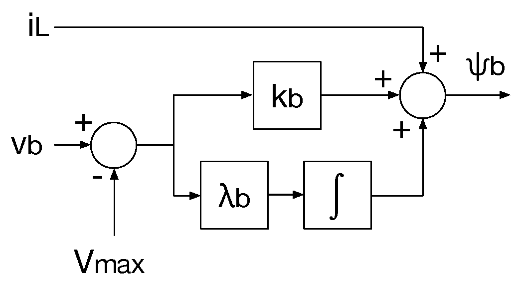
The proposed control system uses one switching function for each operation mode: Ψ p v for MPPT mode and Ψ b for protection mode, which leads to the unified sliding surface ( Φ ) given in Equation (9). Therefore, the system operating at Ψ = 0 is in the sliding-mode with null error, while Ψ 0 corresponds to a system operating far from the reference, hence with an error. The surface includes a binary parameter P r to switch between the two operation modes, depending on the voltage value v b exhibited by the output capacitor, as it is reported in expression (10).
Φ = Ψ p v · 1 P r + Ψ b · P r = 0
if v b < V m a x P r = 0 , Φ = Ψ p v = 0 if v b V m a x P r = 1 , Φ = Ψ b = 0
The switching functions Ψ p v and Ψ b , designed for each mode, are given in Equations (11) and (12), respectively, in which k p v , λ p v , k b and λ b are parameters, i L corresponds to the inductor current of the boost converter, v p v corresponds to the voltage at the PV panel terminals, v m p p t corresponds to the reference provided by the MPPT algorithm, v b corresponds to the output voltage of the DMPPT converter and V m a x is the maximum safe voltage at the converter output terminals.
Ψ p v = i L k p v · v p v v m p p t λ p v · v p v v m p p t d t
Ψ b = i L + k b · v b V m a x + λ b · v b V m a x d t
Both switching functions were designed to share the inductor current, so that the transition between such sliding-mode controllers is not abrupt since the inductor current keeps the same value when P r changes the active sliding function. Figure 7 illustrates the concept of the two operation modes in the proposed control system.
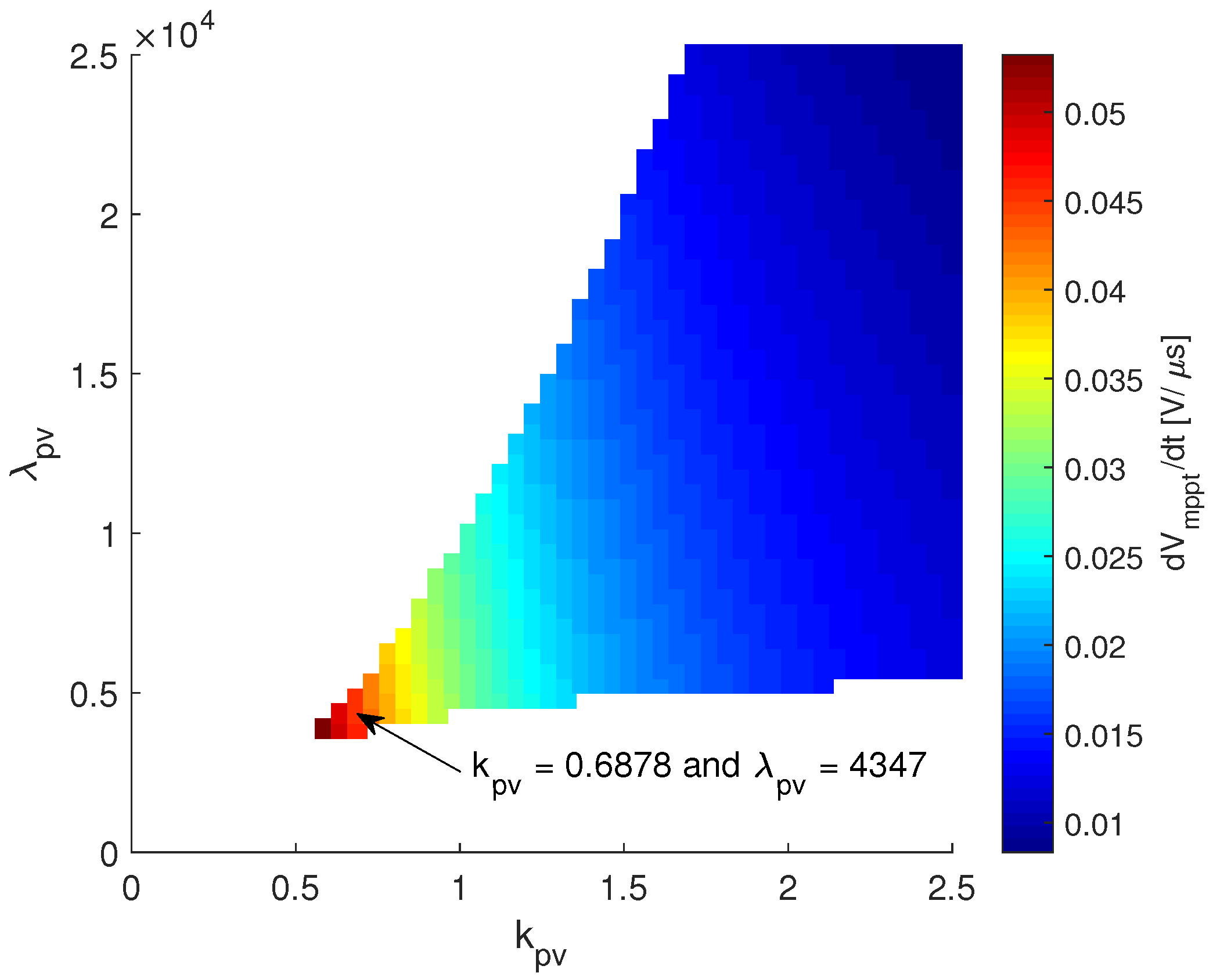
The following section analyzes the stability conditions of the proposed SMC, the equivalent dynamics of the closed loop system, the SMC parameters design, and the implementation of the proposed control system, in both MPPT ( Φ = Ψ p v = 0 ) and Protection ( Φ = Ψ b = 0 ) modes.

4. Analysis of the Proposed SMC

The design process of the sliding-mode control is performed by means of equivalent control method [35]. This technique was used to develop a method for testing convergence, global stability and performance of sliding-mode controllers acting on DC/DC converters, which is based on three considerations: transversality, reachability and equivalent control. Nevertheless, the authors in [35] demonstrated that sliding-mode controllers for DC/DC converters fulfilling the reachability conditions also fulfill the equivalent control condition. Transversality and reachability conditions of the proposed SMC in MPPT and Protection modes are analyzed in Section 4.1 and Section 4.2, respectively. Moreover, the equivalent dynamic model of the DC/DC converter with the SMC is analyzed in Section 4.3 for MPPT and Protection modes.

4.1. Transversality Condition

The transversality condition analyses the ability of the controller to modify the sliding function trajectory. This condition is formalized in Equation (13), which evaluates that the MOSFET control signal u is present into the sliding function derivative [35,36] for MPPT and Protection modes. If the transversality conditions, given in Equation (13), are not fulfilled, the SMC has no effect on the sliding function trajectory and the system is not controllable. The left and right parts of the transversality condition must be fulfilled in MPPT and Protection modes, respectively; therefore, the following subsections analyze the transversality condition in each operation mode.
d d u d Ψ p v d t P r = 0 0 d d u d Ψ b d t P r = 1 0

4.1.1. Transversality Condition in MPPT Mode

In this mode the SMC follows a voltage reference v m p p t provided by an external MPPT algorithm as depicted in Figure 6. In this work it is considered a Perturb and Observe (P&O) MPPT algorithm due to its positive compromise between efficiency and simplicity [39]. In MPPT mode the derivative of the switching function is obtained from Equation (11) as:
d Ψ p v d t = d i L d t k p v · d v p v d t d v m p p t d t λ p v · v p v v m p p t
Replacing the PV voltage and inductor current derivatives, given in Equations (6)–(8), into Equation (14):
d Ψ p v d t = v p v v b · 1 u L k p v · i p v i L C p v + k p v d v m p p t d t λ p v · v p v v m p p t
Finally, the transversality condition is evaluated by replacing Equation (15) into Equation (13), which leads to Equation (16).
d d u d Ψ p v d t = v b L > 0
Since the output voltage is always positive, the transversality value (16) is also positive, which ensures that the transversality condition (13) is fulfilled in any operation condition of MPPT mode. Therefore, the switching function Ψ p v designed for the MPPT mode is suitable to implement a SMC.
Moreover, the positive sign of the transversality value provides information concerning the behavior of a SMC implemented with Ψ p v : d d u d Ψ p v d t > 0 implies that a positive values of u ( u = 1 ) causes a positive change in d Ψ p v d t [35]. In contrast, negative values of u ( u = 0 ) causes a negative change in d Ψ p v d t ; those considerations are used in Section 4.2 to analyze the reachability conditions.

4.1.2. Transversality Condition in Protection Mode

In this mode, the SMC limits the output voltage v b to the maximum acceptable voltage V m a x using the switching function Ψ b introduced in Equation (12). In this mode the derivative of the switching function is obtained from Equation (12) as:
d Ψ b d t = d i L d t + k b · d v b d t d V m a x d t + λ b · v b V m a x
In this mode, the reference V m a x is constant, hence, d V m a x d t = 0 . Replacing that value and the output voltage and inductor current derivatives, in Equations (7) and (8), into Equation (17):
d Ψ b d t = v p v v b · 1 u L + k b · i L · 1 u i d c C b + λ b · v b V m a x
The transversality condition is evaluated by replacing Equation (18) into Equation (13), which leads to expression (19).
d d u d Ψ b d t = v b L k b · i L C b > 0
In expression (19), the transversality condition is defined positive to simplify the circuital implementation of the proposed SMC, as will be shown in Section 6.1. Therefore, the following restriction must be fulfilled by k b :
k b < v b · C b L · i L
Since the design of k b , presented afterwards, takes into account the restriction imposed by expression (20), the transversality condition in expression (13) is fulfilled in any operation condition of the Protection mode. Therefore, the switching function Ψ b designed for the Protection mode is suitable to implement a SMC.
Similar to the MPPT mode, the positive sign of the transversality value in Equation (19) imposes the switching conditions for Ψ b , which are used in the next subsection to analyze the reachability conditions.

4.2. Reachability Conditions and Equivalent Control

The reachability conditions enables the analysis of the conditions in which the SMC successfully tracks the desired surface Φ = Ψ p v = 0 in MPPT mode and Φ = Ψ b = 0 in Protection mode. Considering that the transversality condition is positive for MPPT and Protection modes, the reachability analysis is based on the following conditions [35]: when the switching function of the system is under the surface, the derivative of the switching function must be positive to reach the surface; on the contrary, when the switching function is above the surface, the derivative of the switching function must be negative. Those conditions are formalized in Equations (21) and (22) for MPPT and Protection modes, respectively, which take into account the effect of the transversality value on the switching function derivative explained at the end of Section 4.1.2.
lim Ψ p v 0 d Ψ p v d t u = 1 > 0 lim Ψ p v 0 + d Ψ p v d t u = 0 < 0
lim Ψ b 0 d Ψ b d t u = 1 > 0 lim Ψ b 0 + d Ψ b d t u = 0 < 0
It is worth noting that the equivalent control condition is not included in the stability analysis of the proposed SMC, because Sira-Ramirez demonstrated in [35] that sliding-mode controllers for DC/DC converters fulfilling the reachability conditions also fulfill the equivalent control condition.

4.2.1. Reachability in MPPT Mode

Replacing the explicit expression of the switching function derivative, shown in Equation (15), into expression (21) becomes:
k p v · d v m p p t d t > v p v L + k p v · i p v i L C p v + λ p v · v p v v m p p t
k p v · d v m p p t d t < v p v v b L + k p v · i p v i L C p v + λ p v · v p v v m p p t
From the electrical model in Figure 6 it can be observed that the current of the input capacitor can be defined as i C p v = i p v i L . According to the charge balance principle [40], i C p v = 0 A , which implies that i L and PV current i p v exhibit the same average value, i.e., i p v = i L , otherwise the PV voltage will not be stable. Hence, the only difference between i L and i p v is the high-frequency current ripple present in the inductor, which produces ripples around zero in i p v i L . Therefore, assuming that both inductor and PV currents are approximately equal ( i p v i L ) does not introduce a significant error in the analysis of expressions (23) and (24). This assumption will be validated in simulation results shown in Section 7, where the switching function remains within the hysteresis band in MPPT mode for different operation conditions.
Moreover, the maximum and minimum values of the term v p v v m p p t , assuming a correct operation of the SMC, are Δ v m p p t and Δ v m p p t , respectively, where Δ v m p p t is the size of the voltage perturbation introduced by the P&O algorithm, i.e., max v p v v m p p t = Δ v m p p t and min v p v v m p p t = Δ v m p p t . Finally, the most restrictive case for expression (23) occurs at the minimum values of v p v and v p v v m p p t , while the most restrictive case for expression (24) occurs for the maximum values of v p v and v p v v m p p t , and the minimum value of v b , in which v p v < v b is ensured by boost topology.
In light of the previous considerations, expressions (23) and (24) are rewritten as follows:
d v m p p t d t > 1 k p v min v p v L λ p v · Δ v m p p t
d v m p p t d t < 1 k p v max v p v min v b L + λ p v · Δ v m p p t
Inequalities (25) and (26) impose a dynamic restriction to the reference provided by the MPPT algorithm to guarantee the reachability of the sliding-surface. The main effect of these restrictions is that changes in vmppt cannot be performed in steps, but in ramps that fulfill expressions (25) and (26) [38]. Therefore, if the output of the P&O algorithm fulfills those restrictions the SMC will be able to track the reference in any operation condition. However, those limits depend on the SMC parameters, hence, inequalities (25) and (26) must be evaluated after the design of k p v and λ p v . It is important to note that k p v and λ p v need to be designed in order to provide the highest possible values of d v m p p t / d t limit, in this way, the dynamic restriction of the MPPT algorithm will be reduced. Section 5.3 shows an analysis of d v m p p t / d t limits as well as a numerical example, which illustrates that d v m p p t / d t limit may be in the order of tens of m V / μ s ( kV / s ); hence, the voltage variations can be performed in a small time compared with the perturbation period of the P&O algorithm, which means that restrictions imposed by expressions (25) and (26) do not affect considerably the dynamic performance of the DMPPTU.
In conclusion, the SMC in MPPT mode, i.e., operating with Ψ p v given in Equation (11), is stable if restrictions (25) and (26) are fulfilled.

4.2.2. Reachability in Protection Mode

Replacing the explicit expression of the switching function derivative, Equation (18), into the inequalities introduced in expression (22) leads to:
v p v L k b · i d c C b + λ b · v b V m a x > 0
v p v v b L + k b · i L i d c C b + λ b · v b V m a x < 0
From the electrical model reported in Figure 6, and the power balance principle [40], the loss-less relation between input and output currents and voltages gives i d c i L · v p v / v b , which is used to simplify the reachability analysis. Moreover, fulfilling the reachability conditions ensures a correct operation of the SMC, hence inside the sliding-mode v b = V m a x . Finally, reorganizing expressions (27) and (28) it can be demonstrated that the most restrictive case occurs at the maximum value of i L , which corresponds to the maximum PV current max i L = i p h due to the charge balance condition. The values of v p v and v b are not considered in the worst case, since v b is constant ( v b = V m a x ) and v p v do not influence in the inequalities that define the worst case.
Under the light of the previous considerations, expressions (27) and (28) lead to the same restriction for k b given in expression (20). Therefore, the SMC in Protection mode, i.e., operating with Ψ b given in Equation (12), is stable if the inequality (20) is fulfilled.

4.3. Equivalent Dynamics

The equivalent dynamics correspond to the closed-loop behavior of the system under the action of the SMC. In this case, the equivalent dynamics are calculated by replacing the open-loop differential equation describing the inductor current, Equation (8), with the sliding-surface imposed by the SMC: Ψ p v = 0 in MPPT mode (i.e., Equation (11)), and the sliding-surface imposed by Ψ p v = 0 in Protection mode (i.e., Equation (12)).

4.3.1. Equivalent Dynamics in MPPT Mode

Expressions given in (29) describe the dynamic behavior of the system in MPPT mode, which are obtained replacing Equation (11) in Equation (8). In expression (29), the differential equation describing v p v (Equation (6)) is the same, but the differential equation describing v b (Equation (7)) has been modified to depend on the converter duty cycle d. The converter duty cycle d is defined as the the average value of the signal u within the switching period T s w , as shown in Equation (30). This modification is performed because the MOSFET signal u is imposed by the SMC; hence, the equivalent dynamics disregards the switching ripple in u and it only depends on the average value of the control signal u within the switching period T s w (i.e., d).
d v p v d t = i p v i L C p v d v b d t = i L · 1 d i d c C b i L = k p v · v p v v m p p t + λ p v · v p v v m p p t d t
d = 1 T s w · 0 T s w u d t
The main challenge to analyze the dynamic behavior of Equation (29) corresponds to the non-linear relation between i p v and v p v shown in Equation (1). To overcome this problem, it is necessary to linearize the relation between i p v and v p v around a given operation point. Then, it is possible to obtain the transfer function between the PV panel voltage (controlled variable) and the voltage reference provided by the P&O algorithm. However, it is worth noting that the locations of the poles and zeros of the transfer function vary depending on the operation point where the relation between i p v and v p v is linearized. Hence, the transfer function must be analyzed in different operation points to analyze the dynamic behavior of the system under the action of the proposed SMC.
The small signal relationship between i p v and v p v in a given operation point is reported in Equation (31), where i P V and v P V (uppercase subscripts) are the panel small signal current and voltage, respectively, and Y p v is the PV panel admittance evaluated in a given operation point. Y p v is defined in Equation (32), which is obtained by deriving i p v in Equation (1) with respect to v p v .
i P V = Y p v · v P V
Y p v = i p v v p v = A B exp v p v + R s · i p v B + 1 R h 1 + A · R s B exp v p v + R s · i p v B + R s R h
Replacing Equation (31) into Equation (29), and applying the Laplace transformation, leads to the transfer function between the PV voltage and the reference voltage provided by the P&O algorithm shown in Equation (33), in which V p v ( s ) and V m p p t ( s ) are the Laplace transformations of v P V and v m p p t , respectively.
V p v ( s ) V m p p t ( s ) = k p v C p v · s + λ p v C p v s 2 + k p v Y p v C p v · s + λ p v C p v
Equations (29) and (33) put into evidence that v p v is decoupled from v b due to the action of the SMC, hence, the variations in v b caused by mismatched conditions will not disturb the MPPT action.
However, the transfer function in Equation (33) depends on Y p v , which in turn depends on the operation point of the PV panel; therefore, the variation range of Y p v must be analyzed to perform a correct design of the SMC parameters k p v and λ p v . Considering the same BP585 PV panel used in the previous examples, the current and power curves of such a PV panel are given in Figure 8 for multiple photo-induced currents (i.e., different irradiance conditions) at the expected PV panel temperature ( 298 K ). The data show that the MPP conditions are constrained within the voltage range 16 V < v p v < 19 V , and taking into account that the SMC reference is provided by an MPPT algorithm, then the analysis of Y p v must be performed within the same voltage range.
Figure 9 shows the admittance of the BP585 PV panel, calculated using Equation (32), for the interest voltage range 16 V < v p v < 19 V . The figure put into evidence that Y p v is almost independent from the photo-induced current, which is also observed in Equation (32) because i p v / v p v does not depend directly on i p h . Finally, the admittance range used to design the parameters k p v and λ p v is 0.40 Ω 1 Y p v 0.03 Ω 1 . It must be noted that the analysis of Y p v must be performed for the particular PV panels to be used in the photovoltaic installation.

4.3.2. Equivalent Dynamics in Protection Mode

As in the previous case, the equivalent dynamics are calculated by replacing the open-loop differential equation describing the inductor current, Equation (8), with the sliding-surface imposed by Ψ b = 0 in Equation (12). This procedure is reported in expression (34), in which the differential equation describing v b , Equation (7), has been modified to depend on the converter duty cycle d. Hence the equivalent dynamics disregard the switching ripple.
d v p v d t = i p v i L C p v d v b d t = i L · 1 d i d c C b i L = k b · v b V m a x λ b · v b V m a x d t
The dynamic system in Equation (34) is used to analyze the deviation of v b from V m a x caused by perturbations in the other DMPPT converters connected in series. Applying the Laplace transformation to the previous expression leads to the following transfer function between the output V b ( s ) and reference V m a x ( s ) voltages:
V b ( s ) V m a x ( s ) = 1 d · k b C b · s + 1 d · λ b C b s 2 + 1 d · k b C b · s + 1 d · λ b C b
The dynamic behavior of Equation (35) changes with the duty cycle d, which must be analyzed to design k b and λ b . For the example developed in this paper, the range of the PV voltage is 16 V < v p v < 19 V , which leads to 0.37 < d < 0.68 because v b = V m a x = 50 V . As in the MPPT mode, this analysis of d must be performed for the particular PV panel and dc-link voltage to be used in the photovoltaic installation.

5. Parameters Design of the Proposed SMC

Equivalent dynamic models, introduced in Section 4.3, are used in Section 5.1 and Section 5.2 for the design of the surface parameters k p v , λ p v , k b and λ b to impose a desired close loop dynamics of v p v and v b . Such dynamic behavior is defined as a maximum settling time and a maximum overshoot for all the operation conditions of the DMPPT-U. Furthermore, dynamic restrictions of the proposed SMC are discussed in Section 5.3, while the switching frequencies and hysteresis bands are analyzed in Section 5.4.

5.1. Parameters Design in MPPT Mode

The proposed procedure starts by defining a maximum settling-time ( t s * ) and a maximum overshoot ( M O * ) for v p v considering the restrictions imposed by the MPPT technique. The next step is to identify the feasible couples of parameters k p v , λ p v . A couple k p v , λ p v is feasible if the small signal voltage ( v P V ) settling time ( t s ) and maximum overshoot ( M O ) fulfill t s t s * and M O M O * , for all the possible operation points defined by min Y p v Y p v max Y p v ; where t s and M O , for a given value of Y p v , are calculated from Equation (33). Finally, the feasible couples k p v , λ p v are compared using a proposed indicator and the exact values are selected close to the indicator’s maximum value.
The definition of t s * and M O * is based on the MPPT parameters and power efficiency to provide the following time response criteria:
  • Settling-time t s , which must be shorter than the perturbation period T a of the P&O algorithm to ensure the MPPT stability [41].
  • Maximum Overshoot M O , which must be limited to avoid large deviations from the MPP voltage that produces high power losses.
The evaluation of those criteria requires the calculation of the time response of the PV voltage. Taking into account that the P&O produce step perturbations of Δ v m p p t volts each T a seconds, the PV voltage response is given by Equation (36).
V p v ( s ) = k p v C p v · s + λ p v C p v s 2 + k p v Y p v C p v · s + λ p v C p v · Δ v m p p t s
The time-domain expression of the small signal PV voltage for a particular Y p v ( v P V ( t ) ) is calculated by applying the inverse Laplace transformation to Equation (36), i.e., v P V ( t ) = L 1 V p v ( s ) , which corresponds to the step-response of a second-order system with a real zero.
Appendix A reports the time-domain expressions for the step-response of a canonical second-order system with a real zero for the three possible types of poles: real and different, real and equal, and conjugated complex values. Therefore, V p v ( s ) is rewritten as given in Equation (37) to take profit of the Appendix A expressions.
V p v ( s ) = a · s + b s + p · s + q · 1 s with a = k p v C p v · Δ v m p p t b = λ p v C p v · Δ v m p p t p + q = k p v Y p v C p v p · q = λ p v C p v
Appendix A also reports the expressions for the voltage derivative d v P V ( t ) d t and for the time t M O at which the maximum overshoot M O occurs, i.e., the earliest time for d v P V ( t ) d t = 0 .
Then, the maximum overshoot M O is calculated as shown in Equation (38).
M O = v P V ( t M O )
Similarly, the settling time t s is calculated from Equation (39), which corresponds to the instant in which v P V ( t ) enters into a band of ± ϵ % around the final value Δ v m p p t and keeps trapped inside. Commonly accepted values for the band are ϵ = 2 % , ϵ = 5 % and ϵ = 10 % [42].
v P V ( t s ) Δ v m p p t 1 = ϵ v P V ( t ) Δ v m p p t 1 < ϵ t > t s
Equations (38) and (39) can be solved using different tools: processing the time-domain expressions for v p v ( t ) , given in Appendix A, to calculate both M O and t s as reported in [43]; transforming Equation (36) into differential equations, which must be simulated using numerical methods [44] to find the solutions of Equations (38) and (39); or using specialized functions like stepinfo() from the Control systems toolbox of Matlab [45], which calculates both M O and t s values.
To ensure a correct behavior of the PV voltage, within the MPP range defined in Section 4.3.1, by using the small signal approximation, the SMC parameters k p v and λ p v must ensure that the small signal PV voltage exhibits settling times and maximum overshoots lower than the desired limits t s * and M O * , respectively, for all the admittance values within the interesting range:
M O M O * t s t s * min Y p v Y p v max Y p v
Therefore, a feasible couple k p v , λ p v must fulfill expression (40), where t s and M O are evaluated by using expressions (38) and (39) for each value of Y p v . In this paper, feasible couples k p v , λ p v are identified by using a Monte Carlo analysis [46] to evaluate a wide range of k p v and λ p v values. An example of the obtained results, for t s * = 0.5 ms , ϵ = 5 % , M O * = 10 % , C p v = 22 μ F , Δ v m p p t = 0.5 V , is shown in Figure 10, which reports the valid k p v and λ p v values that fulfill restrictions (40) at the minimum and maximum values of Y p v considering a DMPPT-U formed by a BP585 PV panel, a boost converter constructed with an input capacitor C p v = 22 μ F , and governed by a P&O algorithm with a perturbation magnitude Δ v m p p t = 0.5 V .
The results reported in Figure 10 are useful to analyze the influence of k p v and λ p v into the performance criteria: increasing k p v and λ p v reduce both the settling time and maximum overshoot. However, increasing the values of k p v and λ p v also increases the magnitude of the switching noise transferred into the control system [47]. Therefore, this paper proposes to select k p v and λ p v near the lowest values fulfilling restrictions (40). The selection is performed using the Balance Ratio B R defined in Equation (41), which enables to compare the k p v and λ p v values fulfilling (40) in the entire interest range of the PV admittance.
B R = max 1 2 · t s t s * + 1 2 · M O M O * Y p v min Y p v , max Y p v t s t s * M O M O *
The Balance Ratio for a couple k p v , λ p v is not valid if M O > M O * or t s > t s * in at least one admittance condition. Moreover, the Balance Ratio is equal to one if M O = M O * and t s = t s * in at least one admittance condition. Hence, k p v and λ p v must be selected near the highest Balance Ratio calculated for the DMPPT converter, since a low value of B R implies an increment in k p v and λ p v and, as consequence, an unnecessary increment in both the control effort and the switching noise transferred to the control system [47]. Figure 11 shows the B R values for the example developed in this subsection, where it is observed that the higher values of B R are obtained for the lower feasible values of k p v and λ p v . These results help to select the values k p v = 0.6878 and λ p v = 4347 . Those values provide a B R = 0.8678 , which is close to the maximum condition max B R = 0.9618 , but it is not at the validity frontier. This selection provides a safety margin against tolerances in the elements of the PV system and small differences between the PV voltage and its small signal approximation used to calculate t s and M O for min Y p v Y p v max Y p v .
Figure 12 shows the simulation of equivalent dynamics in the PV voltage, given in Equation (36), considering the designed k p v and λ p v values for the admittance values obtained in the previous subsection. The simulation confirms that both settling time and maximum overshoot of the PV voltage are below the imposed limits in all the admittance conditions. Therefore, the SMC based on Ψ p v (11), and implemented with the selected designed parameters, always fulfills the performance criteria imposed by the expression (40).
In conclusion, this section presented a design process to calculate the parameters of Ψ p v to fulfill both t s t s * and M O M O * , which ensures a correct operation of the associated P&O algorithm and avoids excessive power losses due to transient voltage deviations from the MPP.

5.2. Parameters Design in Protection Mode

The proposed procedure is similar to the one in MPPT mode. The first step is to define the maximum settling-time ( t s * ) and the maximum overshoot ( M O * ) for v b . The second step is to identify the feasible couples of parameters k b , λ b . Finally, the feasible couples k b , λ b are compared by using the Balance Ratio ( B R ) and the exact values are defined close to the maximum value of B R . A couple k b , λ b is feasible if the output voltage ( v b ) t s and M O fulfill t s t s * and M O M O * , for all the possible operation points defined by min d d max d ; where t s and M O , for a given value of d, are calculated from Equation (35).
The evaluation of t s and M O requires to calculate the time response of the output voltage for a perturbation. In this case, it is considered the fastest perturbation possible, which corresponds to a deviation step of magnitude Δ V m a x in v b .
The time-domain expression of the output voltage v b ( t ) , in response to the step perturbation Δ V m a x , corresponds to the step-response of a second-order system with a real zero. Appendix A reports the time-domain expressions for this type of system in canonical form. The Laplace representation of V b ( s ) is rewritten as given in (42) to take profit from the Appendix A expressions.
V b ( s ) = a · s + b s + p · s + q · 1 s with a = 1 d · k b C b · Δ V m a x b = 1 d · λ b C b · Δ V m a x p + q = 1 d · k b C b p · q = 1 d · λ b C b
From the expressions of the voltage derivate and the time t M O , at which the maximum overshoot M O occurs, the following conditions are formulated:
M O = v b ( t M O )
v b ( t s ) Δ V b 1 = ϵ v b ( t ) Δ V b 1 < ϵ t > t s
As discussed in the MPPT mode, Equations (43) and (44) can be solved using different tools. To ensure a correct behavior of the output voltage within the range defined in the previous subsection, the SMC parameters k b and λ b must be analyzed in all the operation range of the Protection mode ( min d d max d ) as given in expression (45), in which t s * and M O * are the desired maximum settling time and maximum overshoot, respectively.
M O M O * t s t s * min d d max d
A feasible couple k b , λ b fulfills expression (45), where M O and t s are calculated by using expressions (43) and (44) for each value of d. As in MPPT mode, feasible k b , λ b are identified using a Monte Carlo analysis for different values of k b and λ b . An example of the obtained results for max d and min d is shown in Figure 13 for t s * = 0.5 ms , ϵ = 2 % , M O * = 5 % , C b = 44 μ F . Such a figure reports the valid k b and λ b values at the minimum and maximum values of d.
The results reported in Figure 13 help to analyze the influence of the parameters into the performance criteria. Moreover, Figure 14 shows the Balance Ratio ( B R ) values for the example developed in this paper, which helps to select the values k b = 1.303 and λ b = 221 . Those values provide a tradeoff between settling-time and overshoot; furthermore, the selected B R = 0.76 provides a safety margin between t s and M O of v b and the limits t s * and M O * for the different operating conditions of the Protection mode.

5.3. Dynamic Restrictions

Dynamic restrictions are only present in MPPT mode, since in Protection mode the reference V m a x is a constant value. Moreover, the reachability analysis in Protection mode (Section 4.2.2) showed that the proposed SMC is stable if expression (20) is fulfilled. Nevertheless, in the analysis of the reachability conditions in MPPT mode (Section 4.2.1) it was demonstrated that dynamic restrictions reported in expressions (25) and (26) must be fulfilled to ensure a stable operation. Those restrictions impose limits to the slew-rate of the voltage reference v m p p t provided by the P&O algorithm.
The example developed up to now is used to illustrate the evaluation of expressions (25) and (26), adopting an inductor L = 330 μ H for the construction of the DMPPT converter. Moreover, the same DC-link voltage levels analyzed in Section 2 are considered, i.e., v d c = 80 V and V m a x = 50 V , and the interesting range of the PV voltage defined in Section 4.3 is also needed, i.e., 16 V < v p v < 19 V . From that information the voltage parameters needed to compute expressions (25) and (26) are calculated: min v p v = 16 V , max v p v = 19 V , min v b = v d c V m a x = 30 V .
Figure 15 reports the limit values for d v m p p t d t to fulfill the dynamic restrictions imposed by expressions (25) and (26). Moreover, the figure also puts into evidence that high values of k p v and λ p v reduce significantly the maximum slew-rate allowed for v m p p t , which could constraint the speed of the P&O algorithm. Therefore, as proposed in the previous subsection, k p v and λ p v must be selected near to the smallest valid values. For example, the adopted values k p v = 0.6878 and λ p v = 4347 impose a d v m p p t d t = 0.0453 V / μ s , which is near to the maximum limit 0.0532 V / μ s achieved at the left-side frontier in Figure 15. In contrast, the highest values for k p v and λ p v reported in Figure 15 will impose a maximum slew-rate equal to 0.0083 V / μ s , which is 5.5 times smaller than the adopted one, hence slowing-down the system response.
This slew-rate limitation for the P&O output signal could be done inside the micro-processor running the MPPT algorithm or using an analog circuit based on operational amplifiers.

5.4. Switching Frequency and Hysteresis Band

Practical implementations of sliding-mode controllers require to add an hysteresis band H around the sliding-surface to constrain the switching frequency to the limits supported by commercial MOSFETs [38]. This section shows the procedure to define H in MPPT and Protection modes to warrant a switching frequency less than a maximum value.

5.4.1. Switching Frequency and Hysteresis Band in MPPT Mode

The practical implementation of Ψ p v requires the transformation of the sliding-surface from Ψ p v = 0 to:
Ψ p v ( t ) < H 2
Due to the SMC operation, in steady state v p v = v m p p t , which imposes an almost constant PV voltage, hence the integral term of v p v v m p p t in Ψ p v is constant in steady-state. In addition, due to the flux balance principle [40], the steady-state inductor current is formed by two components, a constant average value I L and a triangular current ripple δ i L ( t ) with peak amplitude Δ i L . Those conditions impose the following steady-state behavior:
In steady state : k p v · v p v v m p p t 0 λ p v · v p v v m p p t d t I L
Therefore, the steady-state expression for the modified switching function Ψ p v ( t ) is equal to the waveform of the inductor current ripple:
H 2 < Ψ p v ( t ) = δ i L ( t ) < H 2
The peak value Δ i L of δ i L ( t ) is calculated from the differential equation of the inductor current, Equation (8), as given in Equation (49), in which F s w represents the switching frequency and d = v b v p v v b is the duty cycle. Since Ψ p v ( t ) has peak values ± H 2 imposed by the hysteresis band in Equation (48), the value of H that ensures the desired steady-state switching frequency is given by Equation (50).
Δ i L = v p v · d 2 · L · F s w
H = v p v · v b v p v v b · L · F s w
The value of H must be designed for the worst-case scenario of Equation (50) to limit the switching frequency to the MOSFET’s admissible conditions; such a worst-case scenario is obtained by analyzing the minimum values of H. The worst-case value of v b is analyzed using the partial derivative of H, with respect to v b , given in Equation (51): increments in v b produce reductions in H / v b , hence the worst-case corresponds to the maximum value of v b , i.e., V m a x .
H v b = v p v 2 L · F s w · v b 2 > 0
Similarly, the worst-case value of v p v is analyzed using the partial derivative given in Equation (52): if v b > 2 · v p v then the worst-case corresponds to the maximum value of v p v ; if v b < 2 · v p v then the worst-case corresponds to the minimum value of v p v .
H v p v = v b 2 · v p v L · F s w · v b H v p v > 0 if v b > 2 · v p v H v p v < 0 if v b < 2 · v p v
The conditions of the example developed up to now impose v b > 2 · v p v : V m a x = 50 V , min v p v = 16 V and max v p v = 19 V . Hence, to ensure a maximum switching frequency F s w = 40 kHz , the hysteresis band must be set to H = 0.8924 A .

5.4.2. Switching Frequency and Hysteresis Band in Protection Mode

The practical implementation of Ψ b requires to transform the sliding-surface from Ψ b = 0 to:
Ψ b ( t ) < H 2
For the steady-state operation of the SMC it is possible to assume v b = V m a x , hence the integral of v b V m a x in Ψ b is constant. Moreover, as in the MPPT mode, the steady-state inductor current is formed by a constant average value I L and a triangular current ripple δ i L ( t ) with peak amplitude Δ i L . Those conditions impose the following steady-state behavior:
In steady state : k b · v b V m a x 0 λ b · v b V m a x d t I L
Therefore, the steady-state expression of Ψ b ( t ) is given in Equation (55). This expression is analogous to the modified switching function Ψ p v ( t ) of the MPPT mode given in Equation (48), hence the value of H that ensures the desired steady-state switching frequency is the same one obtained for the MPPT mode, i.e., expression (50).
H 2 < Ψ b ( t ) = δ i L ( t ) < H 2
Moreover, the analysis of H developed for the MPPT mode also holds for the Protection mode. Therefore, H = 0.8924 A is calculated for the example developed in the paper, which is the same value obtained for the MPPT mode.

6. Implementation of the Proposed SMC

The explanation of the proposed SMC implementation is divided into two main parts. The first one is introduced in Section 6.1, which focuses on the explanation of the block diagrams to calculate the switching functions Ψ p v and Ψ b , as well as the block diagram of the switching circuit to generate u from Ψ p v , Ψ b and H. The second part is presented in Section 6.2 and it explains the proposed approach to implement the SMC by using a combination of a microprocessor and an analog circuit.

6.1. Implementation Structure

The implementation of the proposed SMC based on Ψ p v and Ψ b includes three main block diagrams: the synthesis of the sliding function Ψ p v , synthesis of the sliding function Ψ b and the switching circuit. It is worth noting that only one switching circuit is required because the transversality sign and value of H are the same in MPPT and Protection modes.

6.1.1. Implementation Structure in MPPT Mode

The on-line calculation of Ψ p v , shown in Equation (11), requires the measurement of the inductor current i L , the PV voltage v p v and the reference provided by the MPPT algorithm with the dynamic restriction analyzed in Section 5.3. Figure 16 presents the block diagram proposed to synthesize Ψ p v , which could be implemented using analog circuits, i.e., Operational Amplifiers (OPAM), or using a digital microprocessor with Analog-to-Digital Converters (ADC) and Digital-to-Analog Converters (DAC). In the digital case, both the calculation of Ψ p v and the limitation of the slew-rate of v m p p t can be implemented in the same microprocessor in charge of processing the P&O algorithm to reduce the complexity, size and cost of the implementation.
The switching law, shown in expression (21), is in charge of producing the MOSFET control signal u. However, due to the introduction of the hysteresis band (see Equation (48)), the modified switching law that must be implemented is introduced in Equation (56).
Ψ p v H 2 set u = 1 ( MOSFET on ) Ψ p v + H 2 set u = 0 ( MOSFET off )
The switching circuit implementing this law is constructed using two analog comparators and a Flip-Flop S-R. The comparators, Comp1 and Comp2, detect the switching conditions to trigger the change of u in the Flip-Flop. Figure 16 presents the proposed switching circuit.

6.1.2. Implementation Structure in Protection Mode

The implementation of the SMC based on Ψ b requires the synthesis of the sliding function and the switching circuit. However, since the transversality sign and value of H are the same ones required to implement Ψ p v , the switching circuit is the same one described in Figure 16.
The block diagram to calculate on-line Ψ b , Equation (12), is presented in Figure 17. This circuit measures the inductor current i L , the output voltage v b and the reference. As in the MPPT mode, the proposed structure could be implemented using analog circuits or a digital microprocessor. The advantage of using a digital implementation concerns the integration of the sliding function calculation for both MPPT and Protection modes into a single device.

6.2. Control System Implementation and Modes Transition

Both SMC components based on Ψ p v and Ψ b are implemented into a single circuit to provide a simple and low cost solution. This is possible, in part, due to the fact that both SMC components exhibit a positive transversality value, Equations (16) and (19), which enable the adoption of the same switching circuit for both modes. Moreover, the structure of the switching functions makes it simple to unify the online calculation of Ψ into a single device. For that purpose, this paper proposes to divide the calculation process of Ψ into two steps: a digital step to process the calculations based on the voltages, and an analog step to process the calculations based on the faster changes present in the inductor current. This approach has been successfully used to implement other SMC for PV systems [38] and to implement SMC with variable switching functions [48], which is the type of solution proposed in this paper.
Then, the calculation of Ψ p v and Ψ b is performed as follows:
  • Digital step: it is executed inside a microprocessor, which measures v p v , i p v and v b , to calculate the intermediate variables i L , p v * and i L , b * reported in Equations (57)–(60), respectively, where the terms int p v and int b are the discrete integral terms of Ψ p v and Ψ b , respectively, processed with the forward Euler method, while δ t corresponds to the time between two measurements performed by the ADC of the microprocessor. Intermediate variables i L , p v * and i L , b * correspond to the algebraic sum of second and third terms of Ψ p v (Equation (11)) and Ψ b (Equation (12)), respectively.
    i L , p v * = k p v · v p v v m p p t λ p v · int p v
    int p v = int p v + δ t · v p v v m p p t
    i L , b * = k b · v b V m a x + λ b · int b
    int b = int b + δ t · v b V m a x
  • Analog step: it adds the measurement of i L with i L , p v * or i L , b * , provided by DAC of the microprocessor, to complete the calculation of Ψ = Ψ p v or Ψ = Ψ b depending on the active mode as reported in Equation (61), where P r was already defined in Equation (10). This process is performed using OPAMs to provide a negligible delay between i L and Ψ ; this is needed to detect the instants in which u must be changed following Equation (48).
    Ψ = i L + i L * with i L * = i L , p v * for P r = 0 i L , b * for P r = 1
Finally, the analog value of Ψ is delivered to the switching circuit, which produces the control signal u driving the MOSFET of the DMPPT converter in both modes.
Figure 18 summarizes the hybrid analog-digital implementation of the proposed solution. The figure also shows the digital implementation of the P&O algorithm and the slew-rate limitation, both operating only in MPPT mode. This avoids the divergence of the P&O algorithm from the MPP zone when the DMPPT converter is operating in Protection mode. In the slew-rate limitation block the term δ V m p p t ( t ) describes the variation of the MPPT reference ( v m p p t ) for each time step ( δ t ), which must fulfill the dynamic restriction in d v m p p t d t imposed by expressions (25) and (26).
Figure 18 also describes the transitions between MPPT and Protection modes:
  • MPPT to Protection: this transition occurs when the output voltage v b reaches the maximum safe value V m a x , which activates the routine for Protection mode ( P r is set to 1). This routine starts by initializing the integral term of Ψ b as given in Equation (62), which forces the inductor current to be close to the value previously defined by the MPPT mode; without this initialization the inductor current will be reset to zero, or to any other value far from its previous condition, which could produce strong perturbations on the DMPPT voltages.
    int b = int b , 0 = i L * λ b
  • Protection to MPPT: this transition occurs when the PV voltage v p v enters the MPPT range, which in the example is 16.5 V < v p v < 18.5 V for the adopted BP585 panel. In such a condition the algorithm sets the variable P r equal to 0, which activates the MPPT mode routine. This routine starts by initializing the integral term of Ψ p v as given in Equation (63) to ensure a stable inductor current in the transition. Entering the MPPT mode enables the operation of the P&O algorithm, which delivers the reference value calculated at the end of the last MPPT mode activation.
    int p v = int p v , 0 = i L * λ p v

7. Simulation Results

The DMPPT system formed by two DMPPT converters connected in series, previously presented in Figure 2, was implemented in the power electronics simulator PSIM to validate the previous analyses. Each DMPPT converter drives a BP585 PV panel with the same circuital implementation presented in Figure 6. The SMC in each DMPPT converter corresponds to the hybrid analog-digital implementation described in Figure 18. Finally, the BP585, boost converter and controller parameters were the same ones defined in the previous sections of the paper: C p v = 22 μ F , L = 330 μ H and C b = 44 μ F for the boost converters, A = 154.15 μ A , B = 1.1088 V 1 , R s = 0.0045 Ω and R h = 109.405 Ω for the BP585 panels and k p v = 0.6878 , λ p v = 4347 , k b = 1.303 , λ b = 221 , Δ v m p p t = 0.5 V , T a = 1 ms , H = 0.8924 , V m a x = 50 V , and d v m p p t d t = 0.0453 V / μ s for the controller.
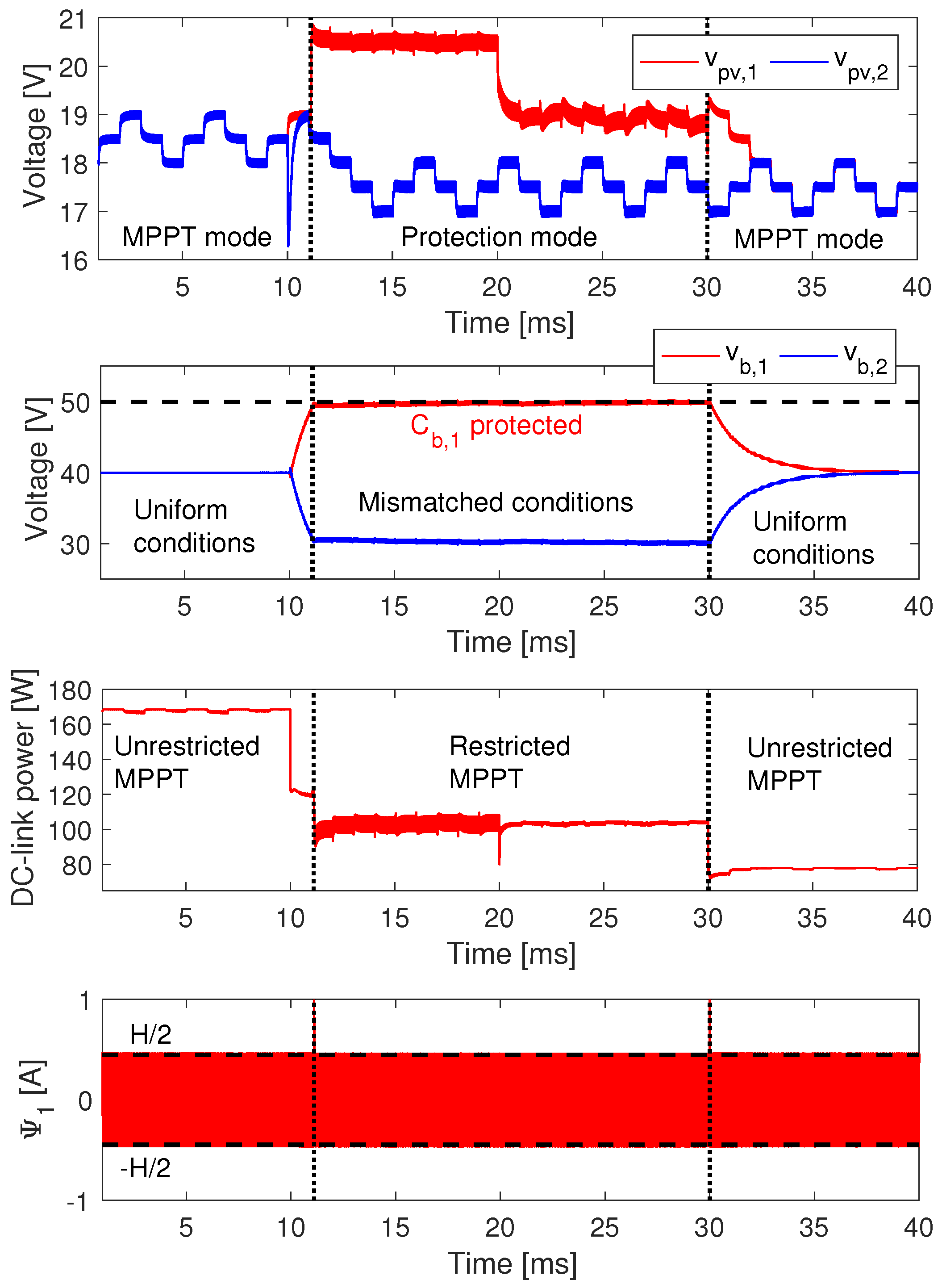
The simulation starts considering the two PV panels operating at 1000 W / m 2 , i.e., in uniform conditions, which forces the output voltages of the DMPPT converters to be equal to 40 V . Figure 19 presents the simulation results, which depicts the operation in MPPT mode of both converters. Then, at 10 ms the irradiance of the second panel drops to 500 W / m 2 , producing a mismatched condition that forces the output voltage of the first DMPPT converter to grow. After 1.1 ms v b , 1 reaches the maximum safe voltage V m a x = 50 V , which triggers the Protection mode. From that moment the PV voltage v p v , 1 of the first panel diverges from the MPP value to reduce the power production, so that the output voltage is limited.
At 20 ms the irradiance of the first PV panel drops to 800 W / m 2 , which requires the system to remain in Protection mode to avoid an overvoltage in C b , 1 . Finally, at 30 ms the irradiance of the first panel drops to 500 W / m 2 , leaving both panels in uniform conditions. Hence, 2.5 μ s latter, the system enters in MPPT mode to start again the tracking of the MPP under safe conditions. The simulation also puts into evidence that the SMC is always stable: the switching function Ψ 1 , corresponding to the DMPPT converter entering in both MPPT and Protection modes, operates inside the hysteresis band H 2 < Ψ 1 < H 2 in both modes under the presence of perturbations in the irradiance, output voltage and P&O reference. However, at the instants in which the modes transition occur ( 11.1060 ms and 30.0025 ms ) the SMC leaves the hysteresis band, but the fulfillment of the reachability conditions forces the SMC to enter again in the band.
Figure 20 shows a zoom of the circuital simulation to verify the design requirements. The figure at the top shows the waveforms of the PV voltage and P&O reference for the first DMPPT-U operating in MPPT mode, which occurs between 6 ms and 8 ms. During that time the PV panel of the first DMPPT-U operates under an irradiance equal to 1000 W/m2, and the SMC successfully fulfills the desired settling time t s 0.5 ms. Similarly, the overshoot is under the 10%. The figure at the middle also shows the waveforms of the PV voltage and P&O reference for the first DMPPT-U operating in MPPT mode, but this time under at irradiance equal to 500 W/m2, which occurs between 36 ms and 38 ms. Again, the SMC successfully fulfills the desired settling time t s 0.5 ms and overshoot ( M O 10 % ). The waveforms described in both MPPT conditions are in agreement with the equivalent dynamics analyses: at 1000 W/m
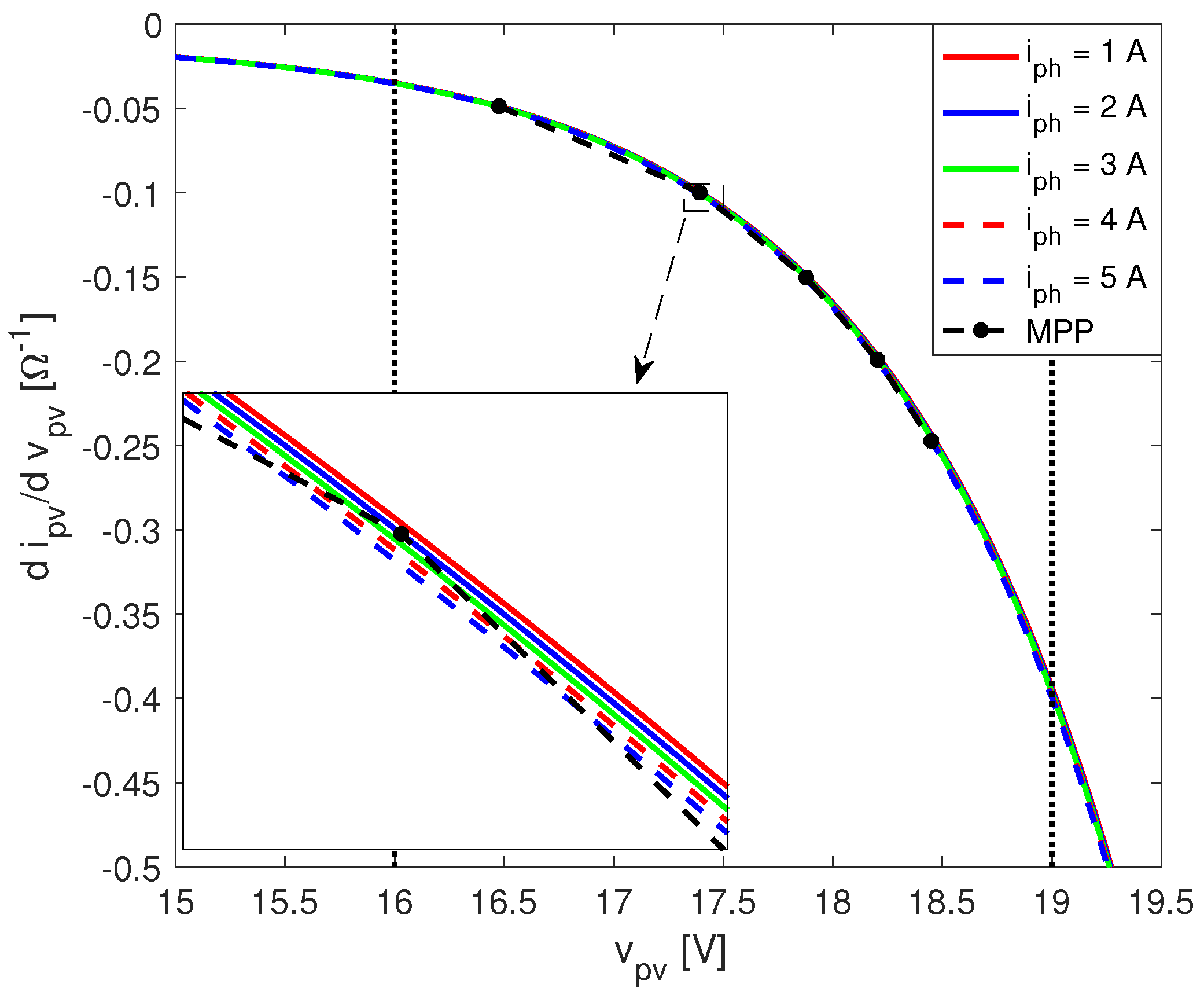
2 the MPP voltage is near 19 V, which corresponds to a PV module admittance near 0.4 Ω 1 according to the data reported in Figure 9. Then, from Figure 12 it is noted that such an admittance describes a PV voltage waveform without any overshoot and with a settling time equal to 0.5 ms, which corresponds to the waveform described by v p v , 1 at the top of Figure 20. Similarly, at 500 W/m2 the MPP voltage is near 18 V, which corresponds to a PV module admittance near 0.16 Ω 1 ; and Figure 12 reports that such an admittance describes a PV voltage waveform without any overshoot and with a settling time much shorter than 0.5 ms, which is equal to the waveform described by v p v , 1 in the middle of Figure 20.
Finally, the bottom of Figure 20 shows the waveform of the output voltage v b , 1 for the first DMPPT-U operating in Protection mode, which occurs between 26 ms and 28 ms. During that time the SMC regulates v b , 1 to avoid an overvoltage condition. The perturbations in v b , 1 are caused by the MPPT action of the second DMPPT-U, which perturbs the overall output power, thus changing the relation between the output voltages of both DMPPT-Us. For example, at 25.9 ms the first DMPPT converter provides 65 W while the second one provides 39 W, which imposes v b , 1 = 50 V and v b , 2 = 30 V ; at 26 ms the SMC of the second DMPPT converter receives a perturbation command from the P&O algorithm, forcing that converter to provide 38.64 W, which in turns changes the output voltages to v b , 1 = 49.72 V and v b , 2 = 30.28 V . However, the simulation confirms that the SMC imposes the desired settling time t s = 0.5 ms to the first DMPPT-U in the regulation of the output voltage v b , 1 under Protection mode. In this case no overshoot is observed.
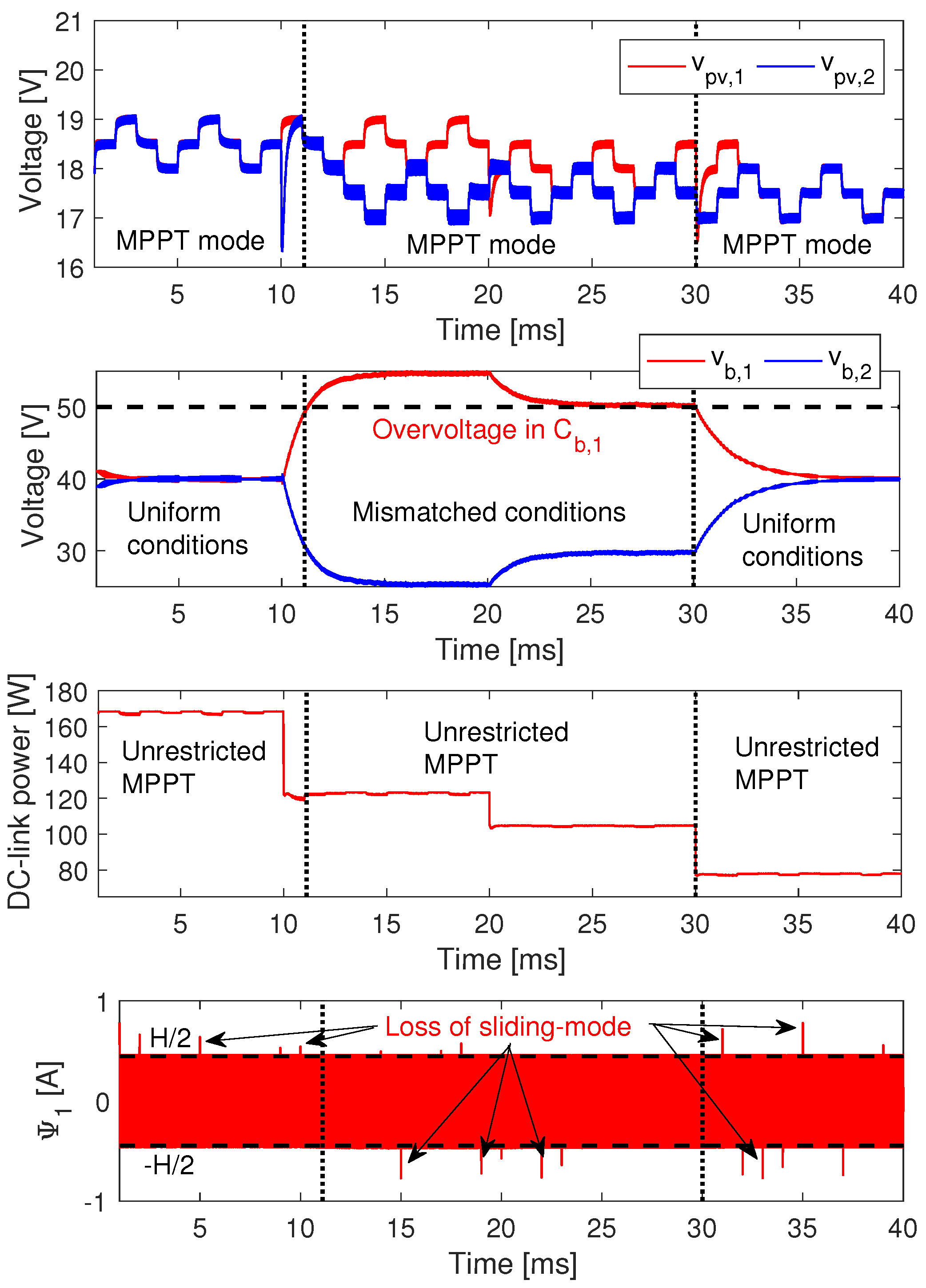
In contrast, Figure 21 shows the simulation of the DMPPT system without activating both the Protection mode and slew-rate limitation. This simulation shows the overvoltage condition that occurs due to the operation in MPPT mode under the mismatching condition, which could destroy C b , 1 and subsequently the DMPPT converters. Moreover, the SMC exhibits loss of the sliding-mode since the switching function Ψ 1 operates outside the hysteresis band due to the lack of dynamic constraints in the P&O reference.
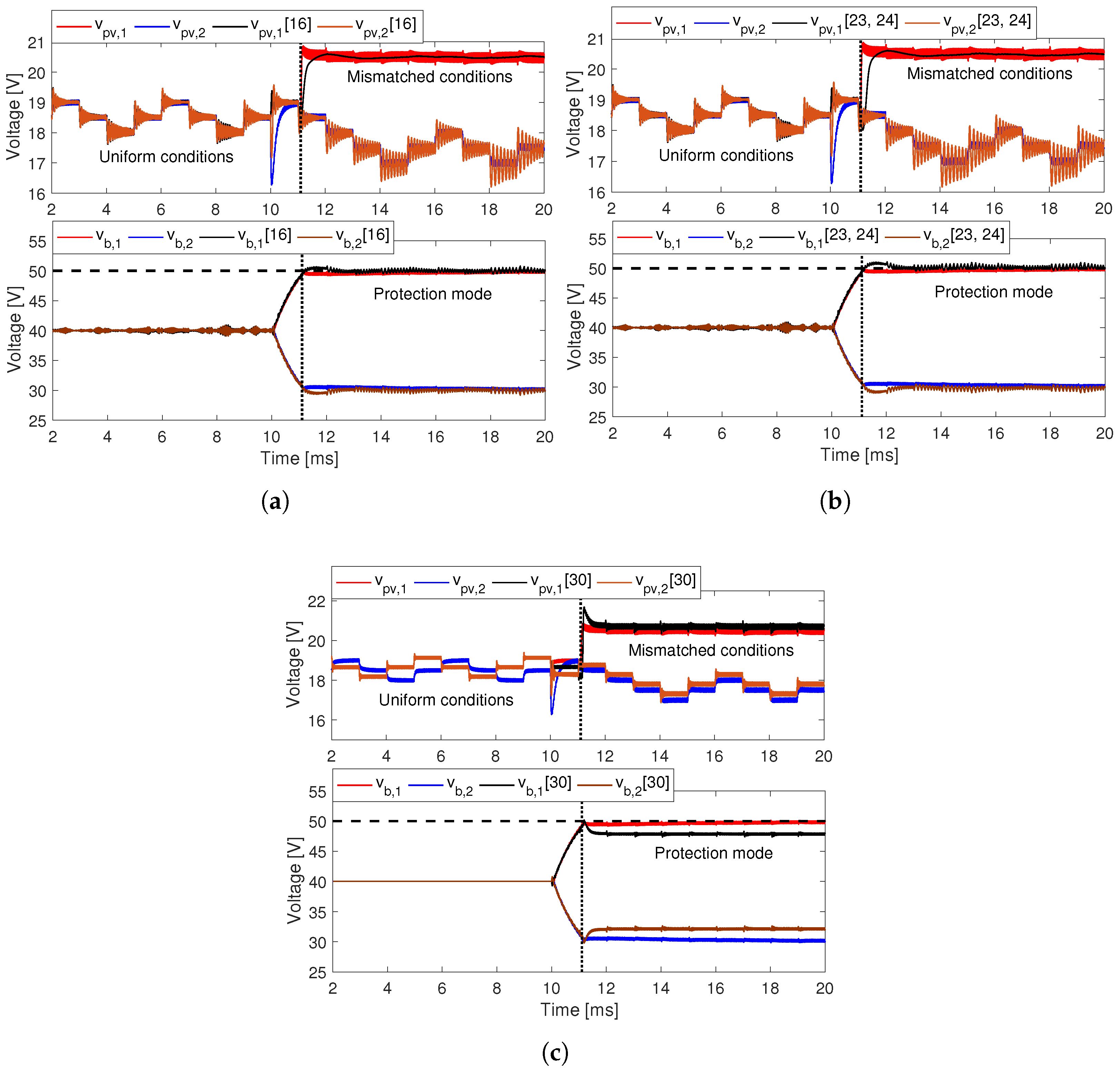
Three DMPPT solutions were implemented to compare their performance with the proposed control strategy, where two of them are some of the most cited papers in double stage DMPPT systems, [16,23,24], and the other is based on SMC [30]. Simulation results introduced in Figure 22 show the comparison of the proposed control strategy with the solutions proposed in [16,23,24,30] respectively.
In [16] the authors use P&O in MPPT mode and fix the duty cycle to keep v b below its maximum value in Protection mode. Results in Figure 22a shows an overshoot in v b , 1 in the transition of the DMPPT-U from MPPT to Protection mode. Such an overshoot surpasses V m a x , which may damage the output capacitor or the switching devices of the DMPPT-U. Moreover, the solution proposed in [16] operates in open-loop during Protection mode and it cannot guarantee the regulation of v b if there are perturbations like variations in the operation points of the other DMPPT-Us or oscillations introduced by the inverter. It is worth noting that the oscillations of v p v obtained with linear regulator are greater than the ones of the proposed SMC. Those oscillations are smaller for high values of v p v and larger for low values of v p v . Additionally, the amplitude of the oscillations increments when one DMPPT-U is in Protection mode.
Solution proposed in [23,24] uses a proportional controller to regulate v b when the DMPPT-U operates in Protection mode. The effect of the proportional controller produces an overshoot in v b , 1 (see Figure 22b) that may damage the output capacitor and switching devices of the boost converter. Additionally, the proportional controller may introduce steady-state errors in and it is not able to reject perturbations produced by the inverter or changes in the operation condition. Even though solution in [23,24] uses Extremum Seeking Control in MPPT mode, the same P&O used in the other solutions were implemented in order to perform a fair comparison in the performance of the DMPPT-U during the transition and regulation in Protection mode.
In [30] the DMPPT-U control is implemented with a SMC in MPPT and Protection modes, however, the SMC does not include integral terms to regulate v p v and v b in the proposed switching function. There is no overshoot in the transition between MPPT and Protection modes (see Figure 22c). Nevertheless, there is a steady-state error in v b , 1 , which forces the DMPPT system to operate in a non-optimal condition, because the optimal condition of a DMPPT in Protection mode is v b = V m a x , as demonstrated in Section 2 and Figure 5. Moreover, the steady-state error in v b is proportional to the current of the DMPPT-U to the DC link, therefore, it is difficult to predict. Solution introduced in [30] also exhibits a steady-state error in v p v and small overshoots, with respect to the proposed solution. That steady-state error is partially compensated by the P&O v p v but deviates the MPPT technique from the MPP.
In conclusion, the simulation results put into evidence the correctness of the design equations and considerations developed in this paper. Moreover, the proposed solution guarantees zero steady-state error in MPPT and Protection modes, no overshoots in v b , and predictable dynamic behaviors in v p v and v b in the entire operation range of the DMPPT-Us.

8. Experimental Implementation and Validation

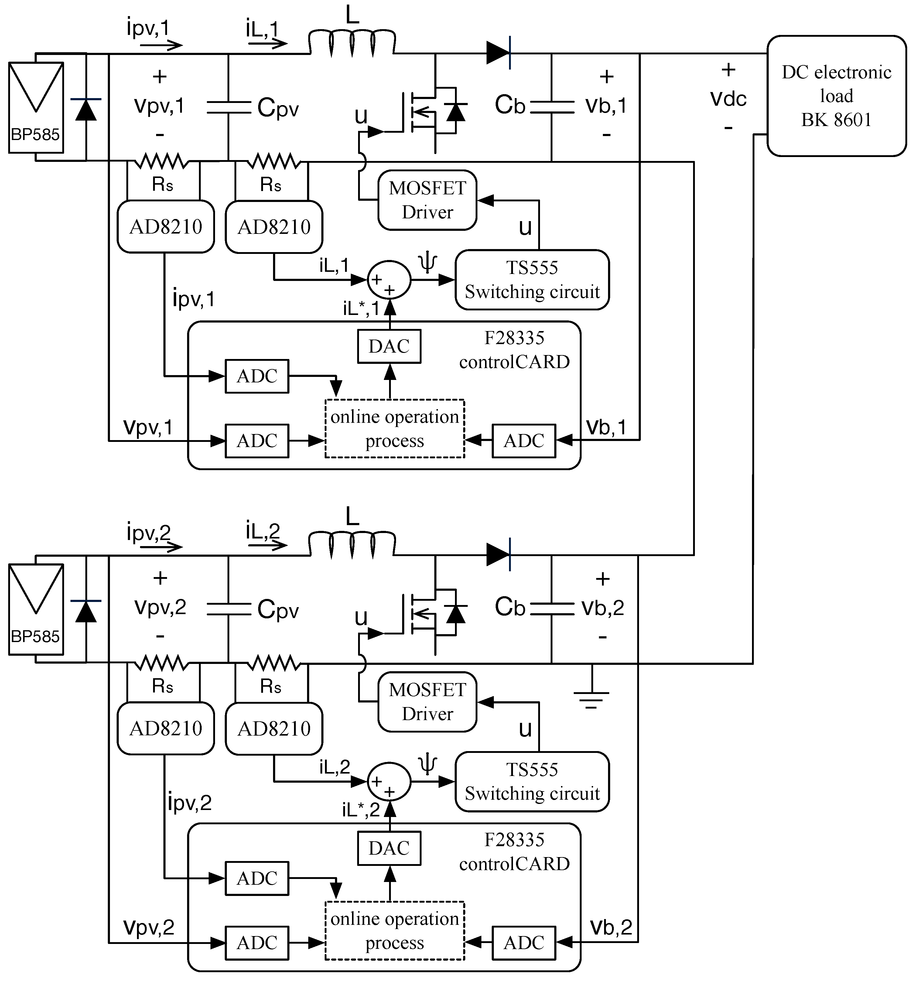
An experimental prototype was developed to validate the proposed solution. The prototype follows the structure adopted in the simulations: it is formed by two DMPPT converters connected in series, each one of them interacting with a BP585 PV panel. The circuital scheme of the prototype is depicted in Figure 23, which reports the implementation of the proposed SMC. The digital steps of the SMC are processed using a DSP F28335 controlCARDs, which have ADC to acquire the current and voltage measurements needed. Both PV and inductor currents are measured using AD8210 circuits and shunt resistors to provide a high-bandwidth, and a MCP4822 DAC (labeled DAC in Figure 23) was used to produce the signals i L , 1 * and i L , 2 * needed to generate the switching functions Ψ . The DSP executes the designed sliding function presented in the structure defined in Figure 18, the result of this operation is converted to an analog value and injected to a circuit based on operational amplifiers, which performs the control action u by means of the TS555 device, based on the implementation presented in [49]. This implementation gives the advantage of computing the high frequency signal ( i L ) by means of analog circuits and the low frequency signal ( i L * ) in a digital form.
The grid-connected inverter reported in Figure 2 was emulated using a BK8601 DC electronic load. Such an electronic load, configured in constant voltage mode, emulates the input voltage control imposed by a traditional grid-connected inverter. 
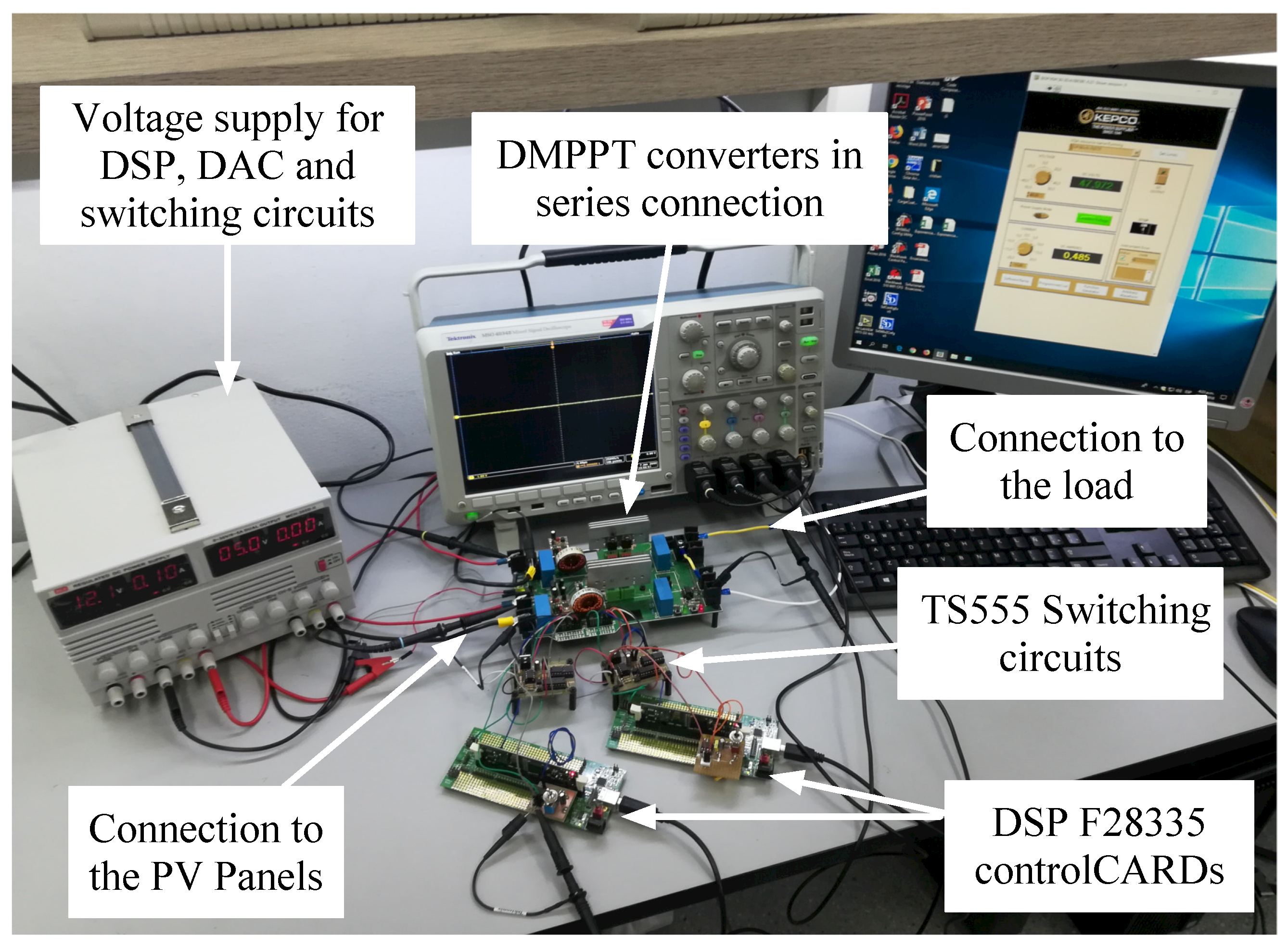
Figure 24 shows the experimental setup, which depicts the two DMPPT converters in series connection. Moreover, the figure also shows the controlCARDs, the TS555 switching circuits, and the connections to both the PV panels and electronic load. Finally, the experimental setup includes a voltage supply used to power the DSP, DAC and switching circuits.
The electrical elements used in the platform are: 2218-H-RC inductors from from Bourns Inc. with L = 330 μ H , MKT1813622016 capacitors from Vishay BC with C p v = 22 μ F and C b = 44 μ F , IRF540N MOSFETs from International Rectifier and MOSFET drivers A3120 from Vishay Semiconductors. The shunt-resistors used to measure the currents were WSL12065L000FEA18 from Vishay Dale with R s = 5 m Ω . Finally, the SMC parameters were the same ones adopted for the simulations. However, the MPPT parameters were changed to Δ v m p p t = 1 V and T a = 1 s due to dynamic limitations of the BK8601 DC electronic load.
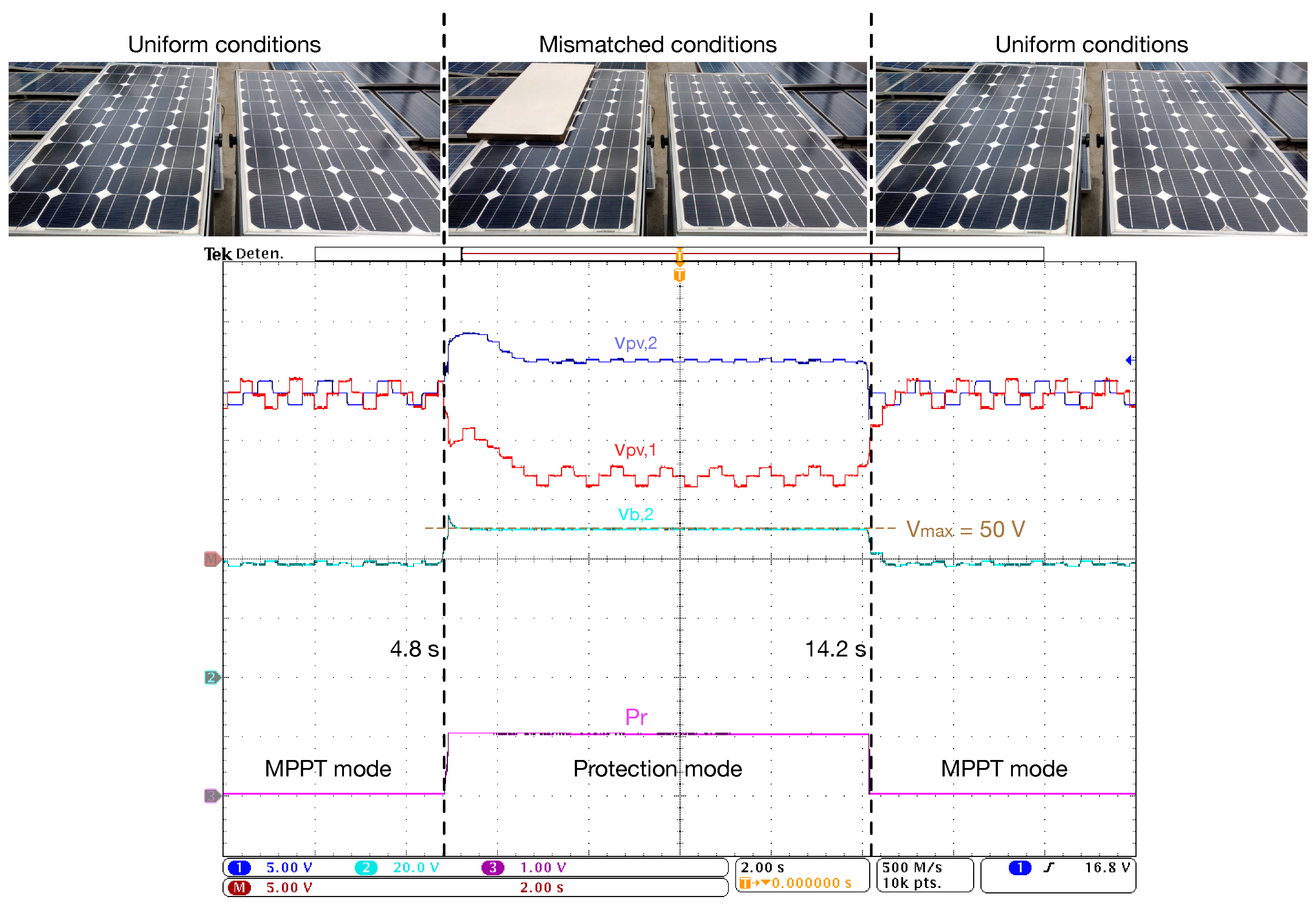
Figure 25 reports the experimental measurements of the prototype. The experiment starts with both BP585 PV panels under uniform conditions, which makes both DMPPT-U operate at the same MPP voltage and power. Therefore, the output voltages of both series-connected DMPPT converters are equal to 40 V , which is under the overvoltage limit V m a x = 50 V . Such conditions force the proposed SMC to operate in MPPT mode, which is evident from the three-point behavior described by both PV voltage profiles v p v , 1 and v p v , 2 . This is also confirmed by signal P r , which is equal to 0 at the start of the experiment.
To emulate a mismatched condition, the first PV panel is partially shaded using an obstacle as it is shown at the top of Figure 25. Therefore, from 4.8 s the first PV panel produces less power than the second PV panel, which forces the output voltage of the second DMPPT converter to grow. Subsequently, the SMC of the second DMPPT-U enters in Protection mode to prevent an overvoltage condition, i.e., P r = 1 , while the SMC of the first DMPPT-U keeps working in MPPT mode. The experiments confirm the correct protection of the second DMPPT converter provided by the proposed SMC.
The obstacle is removed at 14.2 s, which imposes uniform conditions again. Therefore, the SMC of the second DMPPT-U tracks the MPP voltage of the second PV panel by returning to MPPT mode.
In conclusion, the experiment reports a correct operation of the proposed SMC, in both Protection and MPPT modes, under the series-connection.

9. Conclusions

A control strategy based on sliding-mode theory, for DMPPT-Us in double-stage DMPPT architectures, has been presented. The proposed controller is able to perform the MPPT on each PV panel when v b < V m a x (MPPT mode), and to avoid the DMPPT-Us overvoltage under mismatching conditions (Protection mode). The SMC has a single sliding surface able to regulate v p v and v b in MPPT and Protection modes, respectively, including i L into the switching function to provide a soft transition between the two operation modes. Moreover, a detailed design procedure for the SMC parameters and hardware implementation have been provided.
Simulations demonstrate the stability of the DMPPT-Us operating in both MPPT and Protection modes, and also during the transitions between both modes. Moreover, the dynamic performance reported by the simulations fulfills the design restrictions in terms of maximum setting time and overshoot. Furthermore, an experimental platform was developed to show a practical implementation of this new solution. The experimental measurements put into evidence the correct behavior of the practical SMC under real operation conditions.
The proposed control strategy ensures the stability and the dynamic performance of the DMPPT-Us in the entire operation range without a centralized controller or a communication link. Moreover, the control strategy can be implemented using low-cost hardware, which is an important characteristic for commercial DMPPT architectures. This solution can be further improved by implementing observes for both the PV and inductor currents, which will reduce the number of current sensors. Such an approach will reduce both the implementation costs and conduction losses, and it is currently under investigation.

Author Contributions

C.A.R.-P. conceived and developed the theory of the proposed solution; D.G. conceived and performed the experiments; J.D.B.-R. analyzed the data; C.A.R.-P., J.D.B.-R. and D.G. wrote the paper.

Funding

This work was supported by the Universidad Nacional de Colombia, the Instituto Tecnológico Metropolitano, the Universidad Industrial de Santander and Colciencias (Fondo nacional de financiamiento para ciencia, la tecnología y la innovación Francisco José de Caldas) under the projects UNAL-ITM-39823/P17211, “Estrategia de transformación del sector energético Colombiano en el horizonte de 2030—Energetica 2030”—“Generación distribuida de energía eléctrica en Colombia a partir de energía solar y eólica” (Code: 58838, Hermes: 38945) and the doctoral scholarship 2012-567 from Colciencias.

Conflicts of Interest

The authors declare no conflict of interest.

Appendix A. Step Response of the Second Order System with a Zero

This appendix reports the time-domain expressions for the step response and performance criteria for a canonical second-order system with a zero:
v ( t ) = L 1 a · s + b s + p · s + q · 1 s

Appendix A.1. Overdamped System (p and q Are Real and Different)

Time response expression:
v ( t ) = b p q + e p t b a p p p q e q t b a q q p q
Derivative of the time response expression:
d v ( t ) d t = e q t b a q p q e p t b a p p q
Time value at which the M O occurs d v ( t ) d t = 0 :
t M O = ln b a p b a q p q

Appendix A.2. Critically Damped System (p = q Are Real)

Time response expression:
v ( t ) = b p 2 b e p t p 2 t e p t b a p p
Derivative of the time response expression:
d v ( t ) d t = b e p t p + t e p t b a p e p t b a p p
Time value at which the M O occurs d v ( t ) d t = 0 :
t M O = a b a p

Appendix A.3. Under Damped System (p and q Are Complex)

Time response expression:
v ( t ) = b p q b e ( p + q ) t 2 cosh t ( p + q ) 2 4 p q χ p q where χ = sinh t ( p + q ) 2 4 p q ( p + q ) 2 + a p q b ( p + q ) b ( p + q ) 2 4 p q
Derivative of the time response expression:
d v ( t ) d t = b ( p + q ) e ( p + q ) t 2 cosh χ t γ sinh χ t χ 2 p q b e ( p + q ) t 2 χ sinh χ t γ sinh χ t p q where χ = ( p + q ) 2 4 p q γ = ( p + q ) 2 + a p q b ( p + q ) b
Time value at which the M O occurs d v ( t ) d t = 0 :
t M O = ln abs χ ( p + q ) 2 4 p q where χ = 2 p q a 2 ( p + q ) a b + b 2 2 b a ( p + q ) + 2 a ( p + q ) 2 4 p q

References

  1. IEA. 2018 Snapshot of Global Photovoltaic Markets; Technical Report; International Energy Agency: St. Ursen, Switzerland, 2018. [Google Scholar]
  2. Sharkh, S.M.; Abusara, M.A.; Orfanoudakis, G.I.; Hussain, B. Power Electronic Converters for Microgrids; John Wiley & Sons, Singapore Pte. Ltd.: Singapore, 2014. [Google Scholar] [CrossRef]
  3. Mehrasa, M.; Adabi, M.E.; Pouresmaeil, E.; Adabi, J. Passivity-Based Control Technique for Integration of DG Resources into the Power Grid. Int. J. Electr. Power Energy Syst. 2014, 58, 281–290. [Google Scholar] [CrossRef]
  4. Mehrasa, M.; Ebrahim Adabi, M.; Pouresmaeil, E.; Adabi, J.; Jørgensen, B.N. Direct Lyapunov Control (DLC) Technique for Distributed Generation (DG) Technology. Electr. Eng. 2014, 96, 309–321. [Google Scholar] [CrossRef]
  5. Bastidas-Rodríguez, J.D.; Ramos-Paja, C. Types of Inverters and Topologies for Microgrid Applications Tipos de Inversores y Topologías Para Aplicaciones de Microrredes. UIS Ingenierías 2017, 16, 8. [Google Scholar]
  6. Mehrasa, M.; Godina, R.; Pouresmaeil, E.; Vechiu, I.; Rodriguez, R.L.; Catalao, J.P.S. Synchronous Active Proportional Resonant-Based Control Technique for High Penetration of Distributed Generation Units into Power Grids. In Proceedings of the PES Innovative Smart Grid Technologies Conference Europe (ISGT-Europe), Torino, Italy, 26–29 September 2017; pp. 1–6. [Google Scholar] [CrossRef]
  7. Mehrasa, M.; Rezanejhad, M.; Pouresmaeil, E.; Catalao, J.P.S.; Zabihi, S. Analysis and Control of Single-Phase Converters for Integration of Small-Scaled Renewable Energy Sources into the Power Grid. In Proceedings of the 7th Power Electronics and Drive Systems Technologies Conference (PEDSTC), Tehranm, Iran, 16–18 February 2016; pp. 384–389. [Google Scholar] [CrossRef]
  8. Petrone, G.; Ramos-Paja, C.A.; Spagnuolo, G. Photovoltaic Sources Modeling; John Wiley & Sons, Ltd: Chichester, UK, 2017. [Google Scholar] [CrossRef]
  9. Serna-Garcés, S.; Bastidas-Rodríguez, J.; Ramos-Paja, C. Reconfiguration of Urban Photovoltaic Arrays Using Commercial Devices. Energies 2016, 9, 2. [Google Scholar] [CrossRef]
  10. Pendem, S.R.; Mikkili, S. Modelling and Performance Assessment of PV Array Topologies under Partial Shading Conditions to Mitigate the Mismatching Power Losses. Sol. Energy 2018, 160, 303–321. [Google Scholar] [CrossRef]
  11. Bastidas-Rodriguez, J.D.; Franco, E.; Petrone, G.; Ramos-Paja, C.A.; Spagnuolo, G. Maximum power point tracking architectures for photovoltaic systems in mismatching conditions: A review. IET Power Electron. 2014, 7, 1396–1413. [Google Scholar] [CrossRef]
  12. Belhachat, F.; Larbes, C. A Review of Global Maximum Power Point Tracking Techniques of Photovoltaic System under Partial Shading Conditions. Renew. Sustain. Energy Rev. 2018, 92, 513–553. [Google Scholar] [CrossRef]
  13. Das, S.K.; Verma, D.; Nema, S.; Nema, R. Shading Mitigation Techniques: State-of-the-Art in Photovoltaic Applications. Renew. Sustain. Energy Rev. 2017, 78, 369–390. [Google Scholar] [CrossRef]
  14. Kasper, M.; Bortis, D.; Kolar, J.W. Classification and comparative evaluation of PV panel-integrated DC-DC converter concepts. IEEE Trans. Power Electron. 2014, 29, 2511–2526. [Google Scholar] [CrossRef]
  15. Khan, O.; Xiao, W. Review and Qualitative Analysis of Submodule-Level Distributed Power Electronic Solutions in PV Power Systems. Renew. Sustain. Energy Rev. 2017, 76, 516–528. [Google Scholar] [CrossRef]
  16. Femia, N.; Lisi, G.; Petrone, G.; Spagnuolo, G.; Vitelli, M. Distributed Maximum Power Point Tracking of Photovoltaic Arrays: Novel Approach and System Analysis. IEEE Trans. Ind. Electron. 2008, 55, 2610–2621. [Google Scholar] [CrossRef]
  17. Femia, N.; Giovanni, P.; Giovanni, S.; Massimo, V. Distributed Maximum Power Point Tracking of Photovoltaic Arrays. In Power Electronics and Control Techniques for Maximum Energy Harvesting in Photovoltaic Systems; Industrial Electronics; CRC Press: Boca Raton, FL, USA, 2012; pp. 139–249. [Google Scholar] [CrossRef]
  18. Huusari, J.; Suntio, T. Interfacing Constraints of Distributed Maximum Power Point Tracking Converters in Photovoltaic Applications. In Proceedings of the 15th International Power Electronics and Motion Control Conference (EPE/PEMC), Novi Sad, Serbia, 4–6 September 2012. [Google Scholar] [CrossRef]
  19. Wang, F.; Zhu, T.; Zhuo, F.; Yang, Y. Analysis and Comparison of FPP and DPP Structure Based DMPPT PV System. In Proceedings of the 8th International Power Electronics and Motion Control Conference (IPEMC-ECCE Asia), Hefei, China, 22–26 July 2016; pp. 207–211. [Google Scholar] [CrossRef]
  20. Wang, F.; Lee, F.C.; Yue, X.; Zhuo, F. Quantified Evaluation and Criteria Analysis for DMPPT PV System. In Proceedings of the 17th European Conference on Power Electronics and Applications (EPE’15 ECCE-Europe), Geneva, Switzerland, 8–10 September 2015; pp. 1–6. [Google Scholar] [CrossRef]
  21. Lyden, S.; Haque, M. Maximum Power Point Tracking Techniques for Photovoltaic Systems: A Comprehensive Review and Comparative Analysis. Renew. Sustain. Energy Rev. 2015, 52, 1504–1518. [Google Scholar] [CrossRef]
  22. Mohapatra, A.; Nayak, B.; Das, P.; Mohanty, K.B. A Review on MPPT Techniques of PV System under Partial Shading Condition. Renew. Sustain. Energy Rev. 2017, 80, 854–867. [Google Scholar] [CrossRef]
  23. Bratcu, A.I.; Munteanu, I.; Bacha, S.; Picault, D.; Raison, B. Power Optimization Strategy for Cascaded DC-DC Converter Architectures of Photovoltaic Modules. In Proceedings of the 2009 IEEE International Conference on Industrial Technology, Gippsland, VIC, Australia, 10–13 February 2009; pp. 1–8. [Google Scholar] [CrossRef]
  24. Bratcu, A.I.; Munteanu, I.; Bacha, S.; Picault, D.; Raison, B. Cascaded DCDC converter photovoltaic systems: Power optimization issues. IEEE Trans. Ind. Electron. 2011, 58, 403–411. [Google Scholar] [CrossRef]
  25. Renaudineau, H.; Donatantonio, F.; Fontchastagner, J.; Petrone, G.; Spagnuolo, G.; Martin, J.P.; Pierfederici, S. A PSO-based global MPPT technique for distributed PV power generation. IEEE Trans. Ind. Electron. 2015, 62, 1047–1058. [Google Scholar] [CrossRef]
  26. Balato, M.; Vitelli, M. A new control strategy for the optimization of Distributed MPPT in PV applications. Int. J. Electr. Power Energy Syst. 2014, 62, 763–773. [Google Scholar] [CrossRef]
  27. Balato, M.; Vitelli, M. Optimization of distributed maximum power point tracking PV applications: The scan of the Power vs. Voltage input characteristic of the inverter. Int. J. Electr. Power Energy Syst. 2014, 60, 334–346. [Google Scholar] [CrossRef]
  28. Sitbon, M.; Leppäaho, J.; Suntio, T.; Kuperman, A. Dynamics of Photovoltaic-Generator-Interfacing Voltage-Controlled Buck Power Stage. IEEE J. Photovolt. 2015, 5, 633–640. [Google Scholar] [CrossRef]
  29. Ramos-paja, C.A.; Vitelli, M. Distributed Maximum Power Point Tracking with Overvoltage Protection for Pv Systems Seguimiento Distribuido Del Punto De Maxima Potencia Con Proteccion De Sobrevoltaje. Dyna 2013, 80, 141–150. [Google Scholar]
  30. Ramos-Paja, C.A.; Saavedra-Montes, A.J. Overvoltage protection for distributed maximum power point tracking converters in series connection. In Applied Computer Sciences in Engineering, Proceedings of the Third Workshop on Engineering Applications (WEA 2016), Bogotá, Colombia, 21–23 September 2016; Springer International Publishing: Berlin, Germany, 2016; pp. 308–319. [Google Scholar]
  31. Bastidas, J.D.; Franco, E.; Petrone, G.; Ramos-Paja, C.A.; Spagnuolo, G. A model of photovoltaic fields in mismatching conditions featuring calculation speed. Electr. Power Syst. Res. 2013, 96, 81–90. [Google Scholar] [CrossRef]
  32. Accarino, J.; Petrone, G.; Ramos-Paja, C.A.; Spagnuolo, G. Symbolic algebra for the calculation of the series and parallel resistances in PV module model. In Proceedings of the 2013 International Conference on Clean Electrical Power (ICCEP), Alghero, Italy, 11–13 June 2013; pp. 62–66. [Google Scholar] [CrossRef]
  33. Balato, M.; Vitelli, M.; Femia, N.; Petrone, G.; Spagnuolo, G. Factors limiting the efficiency of DMPPT in PV applications. In Proceedings of the 3rd International Conference on Clean Electrical Power: Renewable Energy Resources Impact (ICCEP), Ischia, Italy, 14–16 June 2011; pp. 604–608. [Google Scholar] [CrossRef]
  34. Mastromauro, R.A.; Liserre, M.; Dell’Aquila, A. Control issues in single-stage photovoltaic systems: MPPT, current and voltage control. IEEE Trans. Ind. Inf. 2012, 8, 241–254. [Google Scholar] [CrossRef]
  35. Sira-Ramirez, H. Sliding Motions in Bilinear Switched Networks. IEEE Trans. Circuits Syst. 1987, 34, 919–933. [Google Scholar] [CrossRef]
  36. Tan, S.C.; Lai, Y.; Tse, C.K. General Design Issues of Sliding-Mode Controllers in DC-DC Converters. IEEE Trans. Ind. Electron. 2008, 55, 1160–1174. [Google Scholar] [CrossRef] [Green Version]
  37. Chatrenour, N.; Razmi, H.; Doagou-Mojarrad, H. Improved double integral sliding mode MPPT controller based parameter estimation for a stand-alone photovoltaic system. Energy Convers. Manag. 2017, 139, 97–109. [Google Scholar] [CrossRef]
  38. Montoya, D.G.; Ramos-Paja, C.A.; Giral, R. Improved Design of Sliding-Mode Controllers Based on the Requirements of MPPT Techniques. IEEE Trans. Power Electron. 2016, 31, 235–247. [Google Scholar] [CrossRef]
  39. Nicola, F.; Giovanni, P.; Giovanni, S.; Massimo, V. Maximum Power Point Tracking. In Power Electronics and Control Techniques for Maximum Energy Harvesting in Photovoltaic Systems; Industrial Electronics; CRC Press: Boca Raton, FL, USA, 2012; pp. 35–87. [Google Scholar] [CrossRef]
  40. Erickson, R.W.; Maksimovic, D. Fundamentals of Power Electronics, 2nd ed.; Kluwer Academic Publishers: New York, NY, USA, 2001. [Google Scholar]
  41. Petrone, G.; Ramos-Paja, C.A.; Spagnuolo, G.; Vitelli, M. Granular control of photovoltaic arrays by means of a multi-output Maximum Power Point Tracking algorithm. Prog. Photovolt. Res. Appl. 2012, 21. [Google Scholar] [CrossRef]
  42. Golnaraghi, F.; Kuo, B.C. Automatic Control Systems, 9th ed.; John Wiley & Sons, Inc.: Hoboken, NJ, USA, 2010. [Google Scholar]
  43. Ramos-Paja, C.A.; González, D.; Saavedra-Montes, A.J. Accurate calculation of settling time in second order systems: A photovoltaic application. Revista Facultad de Ingenieria 2013, 104–117. [Google Scholar]
  44. Press, W.H.; Teukolsky, S.A.; Vetterling, W.T.; Flannery, B.P. Numerical Recipes in C: The Art of Scientific Computing, 2nd ed.; Cambridge University Press: Cambridge, UK, 1988. [Google Scholar] [CrossRef]
  45. Matworks. Rise Time, Settling Time, and Other Step-Response Characteristics—MATLAB Stepinfo. Available online: http://www.mathworks.com/help/control/ref/stepinfo.html (accessed on 24 August 2018).
  46. Hammersley, J.M.; Handscomb, D.C.; Weiss, G. Monte Carlo Methods, 2nd ed.; Wiley-VCH: Hoboken, NJ, USA, 2008. [Google Scholar]
  47. Kapat, S.; Krein, P.T. Formulation of PID control for DC-DC converters based on capacitor current: A geometric context. IEEE Trans. Power Electron. 2012, 27, 1424–1432. [Google Scholar] [CrossRef]
  48. Serna-Garcés, S.I.; Gonzalez-Montoya, D.; Ramos-Paja, C.A. Sliding-mode control of a charger/discharger DC/DC converter for DC-bus regulation in renewable power systems. Energies 2016, 9, 245. [Google Scholar] [CrossRef]
  49. Montoya, D.G.; Paja, C.A.R.; Giral, R. Maximum power point tracking of photovoltaic systems based on the sliding mode control of the module admittance. Electr. Power Syst. Res. 2016, 136, 125–134. [Google Scholar] [CrossRef]
Figure 1. Centralized MPPT system based on a double-stage structure.
Energies 11 02220 g001
Figure 2. Distributed MPPT system based on a double-stage structure.
Energies 11 02220 g002
Figure 3. Electrical behavior of a mismatched PV string with two PV panels.
Energies 11 02220 g003
Figure 4. Theoretical power production of the DMPPT system in Figure 2.
Energies 11 02220 g004
Figure 5. Safe power production of the DMPPT system in Figure 2.
Energies 11 02220 g005
Figure 6. Electrical model of a DMPPT boost converter.
Energies 11 02220 g006
Figure 7. Concept of the proposed operation modes and sliding surfaces.
Energies 11 02220 g007
Figure 8. Current and power curves of the BP585 PV panel for 1 A < i p h < 5 A .
Energies 11 02220 g008
Figure 9. Admittance of the BP585 PV panel for 16 V < v p v < 19 V and 1 A < i p h < 5 A .
Energies 11 02220 g009
Figure 10. k p v and λ p v values that fulfill restrictions in expression (40) for min Y p v and max Y p v conditions.
Energies 11 02220 g010
Figure 11. Balance Ratio for k p v and λ p v values that fulfill restrictions in expression (40).
Energies 11 02220 g011
Figure 12. Simulation of the equivalent dynamics in the PV voltage for k p v = 0.6878 and λ p v = 4347 .
Energies 11 02220 g012
Figure 13. k b and λ b values that fulfill restrictions in expression (45) for min d and max d conditions.
Energies 11 02220 g013
Figure 14. Balance Ratio for k b and λ b values that fulfill restrictions in expression (45).
Energies 11 02220 g014
Figure 15. Limit values for d v m p p t d t to fulfill the dynamic restrictions imposed by expressions (25) and (26).
Energies 11 02220 g015
Figure 16. Block diagram implementation of the SMC for the MPPT mode.
Energies 11 02220 g016
Figure 17. Block diagram to synthesize Ψ b in Protection mode.
Energies 11 02220 g017
Figure 18. Implementation of the control system.
Energies 11 02220 g018
Figure 19. Simulation of the DMPPT system with the proposed control structure.
Energies 11 02220 g019
Figure 20. Zoom of the simulations in both MPPT and Protection modes.
Energies 11 02220 g020
Figure 21. Simulation of the DMPPT system without activating both the Protection mode and slew-rate limitation.
Energies 11 02220 g021
Figure 22. Comparison of the proposed solution with other DMPPT control strategies with Protection mode. (a) Comparison with DMPPT control proposed in [16]. (b) Comparison with DMPPT control proposed in [23,24]. (c) Comparison with DMPPT control proposed in [30].
Energies 11 02220 g022
Figure 23. Circuital scheme of the experimental prototype.
Energies 11 02220 g023
Figure 24. Experimental setup.
Energies 11 02220 g024
Figure 25. Experimental measurements.
Energies 11 02220 g025

