Rapid Processing of Wafer-Scale Anti-Reflecting 3D Hierarchical Structures on Silicon and Its Templation


1
Amity Institute of Nanotechnology, Amity University Uttar Pradesh, Noida 201301, UP, India
2
School of Pharmacy, The University of Queensland, Brisbane, QLD 4102, Australia
*
Authors to whom correspondence should be addressed.
Materials 2018, 11(12), 2586; https://doi.org/10.3390/ma11122586
Submission received: 30 November 2018
/
Revised: 11 December 2018
/
Accepted: 15 December 2018
/
Published: 18 December 2018
(This article belongs to the Special Issue Anodized Nanoporous Materials: Porous Silicon, Nanoporous Alumina, and Titania Nanotube Arrays)
Abstract
:Hierarchically structured silicon (Si) surfaces with a combination of micro/nano-structures are highly explored for their unique surface and optical properties. In this context, we propose a rapid and facile electroless method to realize hierarchical structures on an entire Si wafer of 3″ diameter. The overall process takes only 65 s to complete, unlike any conventional wet chemical approach that often combines a wet anisotropic etching of (100) Si followed by a metal nanoparticle catalyst etching. Hierarchical surface texturing on Si demonstrates a broadband highly reduced reflectance with average R% ~ 2.7% within 300–1400 nm wavelength. The as-fabricated hierarchical structured Si was also templated on a thin transparent layer of Polydimethylsiloxane (PDMS) that further demonstrated prospects for improved solar encapsulation with high optical clarity and low reflectance (90% and 2.8%).
1. Introduction
There has been an exponential growth in the field of micro/nano-texturing of a silicon (Si) surface due to its attractive properties like controllable surface wettability and optical properties [1,2,3]. Especially hierarchical structures with a unique combination of micro/nano-structures on Si that makes them highly useful for applications like self-cleaning, solar cell, photoluminescence, contamination prevention, etc. [3,4,5]. Various techniques like vapor-liquid-solid (VLS), reactive ion etching (RIE), electrochemical etching, and wet anisotropic electroless etching have been used for fabricating micro and nano-structures on Si surfaces [5,6,7,8,9]. However, methods like VLS and RIE are expensive and complicated. Despite the ease and simple process of wet electrochemical and electroless etching, they result in a non-uniform and poorly controllable porous structure. Furthermore, the type of micro/nano pattern generated using wet chemical etching is dependent on the crystal orientation. For example, chemical etching of (100) Si crystal orientation generates pyramid like structures, whereas anisotropic etching of (110) Si results in the generation of micro-structures with vertical side walls [10,11]. The reason behind the growth of pyramid shaped micro-structure in (100) Si is due to the presence of two dangling bonds and two back bonds in each atom of (100) Si. Thus a low activation energy is required to remove an atom from the (100) lattice; hence, (100) Si experiences faster etching with alkaline etchant solution than other surface orientations [12]. Nanotexturing on Si surface using metal nanoparticle assisted etching has also been reported [4,13,14,15,16]. Electroless etching using metal nanoparticles is a rather rapid and facile process. There are several reports where wet chemical anisotropic etching (in potassium hydroxide (KOH)) and metal nanoparticle assisted etching process has been combined to realize hierarchical structures on Si [2,3,17]. Superhydrophobicity with a water contact angle (WCA) as high as 166° on the Si surface using conventional KOH based etching combined with gold nanoparticle assisted etching followed by a treatment with perfluorooctyl trichlorosilane (PFTOS), has been demonstrated in the literature [2]. However, the superhydrophobicity is imparted by the self-assembled monolayer (SAM) of PFTOS that are known to be adversely affected by environmental conditions. Besides superhydrophobicity, hierarchical texturing on Si surface have also been demonstrated to exhibit improved broadband anti-reflection property. The literature has demonstrated a WCA of 165° and an average optical reflectance of 4% over a wavelength of 450–2500 nm on a hierarchically textured Si surface [3]. Other than the metal nanoparticle assisted etching technique, hierarchical structuring on Si has also been described using e-beam lithography inductively coupled with plasma etching, etc. Si surfaces with reflection as low as 2% have been created using these techniques, however, most of these processes are complex, expensive, and time consuming [18,19].
Additionally, inverted micro/nano-pyramid structures developed using micro/nano structured Si templates have also shown bright prospects towards light trapping [20,21,22,23,24,25,26,27]. Due to their V-shaped architecture, the incident light experiences multiple internal reflections along the side walls that overall leads to minimized reflection of light than the vertically grown pyramid micro-structures. According to previous literature, micro-scaled inverted pyramidal structures were fabricated by metal nanoparticle assisted etching technique [20,21,22,23], whereas fabrication of nano-scale pyramids employed a combination of wet alkaline etching and photolithography technique [24,25,26,27]. However, due to the complexity and high cost, the photolithography process may not be preferred for high throughput commercial fabrication. The formation of inverted pyramidal structures on Si depends on substrate orientation. This implies the occurrence of faster Si etching initiating along direction (100) and terminating at (111) plane, and overall it forms an inverted pyramidal architecture (upright if etched with an alkaline solution). Comparative to (100) configuration metal assisted etching performed on (110) Si and (111) Si, results in the formation of rhombus shaped and triangular/hexagonal shaped structures, respectively [23]. According to Chen et al. these rhombus and triangular shaped structures formed on (110) Si (110) and (111) Si offers poor light management comparative to inverted pyramid structures formed on (100) Si [23].
It is clear that most reports on the anti-reflecting surface of Si involve either a three-step process [3,17,28] or a single step etching of longer duration [21]. Lack of a simple and rapid process to generate anti-reflecting Si surface has motivated us to develop a fast and facile electroless method to fabricate uniform hierarchical micro/nano-structures on Si over a large area. Unlike the previous literature based on the fabrication of hierarchical structure on Si wafer using three-step texturing process; our proposed two-step method was made possible by selecting the unpolished side of a commercial (100) Si wafer that was pre-textured with micron dimension square shaped indents. These square micro-structures often result during the polishing step of a Si wafer during the lapping process. Further, nanotexturing on this micro-structured Si surface using a conventional silver (Ag) nanoparticle assisted etching process resulted in the formation of nanoscale pits on its surface. The as-obtained hierarchical structured Si was further used as a template to pattern a thin PDMS layer for potential application as a solar encapsulation material. Here, we demonstrate the fabrication of a wafer-scale hierarchically textured Si template (3″ diameter) and imprinting of a thin PDMS layer thereof. The patterned PDMS layer was identified to have excellent anti-reflection and high transmittance.
2. Materials and Methods
2.1. Materials
A 3″ diameter single side polished (100) plane n-type (phosphorus doped) Si wafer (Vinkarola), Sylgard 184 PDMS kit (Dow Corning), hydrofluoric acid (40 wt%), nitric acid (68 wt%), silver nitrate, n-hexane, and hydrogen peroxide (30 wt%) were purchased from Merck (Burlington, MA, USA). For coating, the structurally engineered Si wafer, 1-trichloro (1H,1H,2H,2H-perfluorooctyl) silane, was obtained from Sigma Aldrich (India). All chemicals and salts used were analytical grade. DI water (18 MΩ cm) was used to prepare all the solutions.
2.2. Methodology
2.2.1. Fabrication of Hierarchically Structured Si
Si wafers were cleaned using standard RCA cleaning protocol and stored in a vacuum desiccator till further experiments were conducted. The detailed method for metal nanoparticle assisted etching using Ag nanoparticles has been adopted from previous literature [3,14,15,29]. In brief, a mixed aqueous solution of 0.01 M of silver nitrate (AgNO3) and 4.6 M hydrofluoric acid (HF) was prepared at room temperature. Important Note: Hydrofluoric acid (HF) is a highly corrosive and toxic acid, thus any exposure to HF should be avoided. The deposition of Ag nanoparticles was performed in dark condition for variable time intervals of 30 s, 60 s, and 120 s. The wafers were gently cleaned and dried before the next processing step. Further, the Si wafers deposited with Ag nanoparticles were etched in a solution of hydrofluoric acid (HF), hydrogen peroxide (H2O2), and DI water mixed in a volume ratio of 1:5:10 at room temperature. Etching was performed for three different time durations for 5 s, 10 s, and 20 s under dark condition. The etched samples were then washed thoroughly in DI water and further dipped in nitric acid (HNO3) to remove the Ag nanoparticles deposited on the Si surface. After repeated washing in DI water and ultrasonication, the etched Si samples were dried and systematically analyzed. The micro/nano-dimension features on the Si surface (SEM image) were measured using ImageJ (free image analysis tool developed by the National Institutes of Health, NIH, USA) software.
2.2.2. Patterning PDMS
Before spin coating the PDMS pre-polymer mix, the etched Si wafer was treated with a self-assembled monolayer (SAM) of 1-Trichloro (1H,1H,2H,2H-perfluorooctyl) silane to make the Si surface super-hydrophobic so that cured PDMS could be easily peeled off. After pre-treatment of the Si template, PDMS pre-polymer and curing agent were mixed in a ratio of 10:1 w/w and degassed to remove the bubbles generated during the mixing process. The mixture was then diluted with n-hexane with 1:1 v/v and spin coated onto the Si wafer and cured at 120 °C for 10 min. The cured PDMS layer was then peeled off from the Si surface. Dilution was necessary to lower the viscosity of the PDMS pre-polymer mix so as to ensure its capillary filling inside the pores of the etched Si. The process of hierarchical patterning of PDMS is schematically illustrated in Scheme 1.
2.2.3. Physical and Optical Characterization
A Zeiss-EVO 18-448Scanning electron microscope. with EDX detector attachment (Zeiss, Germany) was used for structural analysis. UV-Vis-NIR spectrophotometer (Shimadzu-UV 2600, Japan). equipped with integrating sphere (ISR-2600 plus) attachment was used for the transmission and reflection measurements. Optical measurements were measured from five different positions of the etched Si wafer and patterned PDMS. The integrating sphere is equipped with two detectors—photomultiplier tube (PMT) and InGaAs and can scan wavelengths from 220 nm to 1400 nm. During diffused reflectance measurement, the incident beam of light is directed to the sample surface at an incidence angle of 0° and for specular reflectance measurement, the light is directed at an incident angle of 8° on the sample surface. All the transmission measurements performed on the PDMS membrane were a direct measurement. Further, reflection and transmission measurements were acquired at five different positions of the etched Si wafer and patterned PDMS.
3. Results
3.1. Structural Analysis of Ag Nanoparticle Deposited Si Wafer
The scanning electron microscope (SEM) image in Figure 1 shows the surface morphology of the unpolished side of a Si wafer. The unpolished side of the Si wafer comprises of square-shaped indented micro-structure with an average dimension of 25 µm × 35 µm × 3 µm (l × b × h). A magnified view of the lapped micro-structures is shown in the inset.
Three different time intervals of 30 s, 60 s, and 120 s were used for electroless deposition of Ag nanoparticles on the unpolished side of the Si wafer. Ag nanoparticles, when deposited for a time span of 30 s, resulted in low surface area coverage on Si as shown in Figure 2a and clearly visible in the magnified view shown in the corresponding inset. Increasing the deposition time to 60 s resulted in an improved surface coverage with uniform inter-particle spacing (Figure 2b). The average dimension of the Ag nanoparticles was measured between 150 nm and 170 nm (using ImageJ) as can be observed from the inset of Figure 2b. On further increasing the time duration up to 120 s, an excess growth of Ag nano-structures was observed as shown in Figure 2c. By doubling the deposition time a vigorous increase in particle growth rate is experienced, however, a more intense particle growth is observed across the edges of square micro-structures. Comparative to inner space, the Ag nanoparticles across the edges were experiencing a faster growth rate and an increased deposition time allowed them to transform into branched structures (inset of Figure 2c). Presence of dendritic Ag micro/nano-structures masked the entire substrate (Si) that limited its exposure during HF etching. Moreover, due to excessive multilayered growth, the Ag dendrites appeared to physically detach from the underlying Si surface. Thus, Ag deposition time of 60 s was chosen due to uniform Ag coverage, controlled moderate interparticle-spacing, and strong adhesion between the nanoparticles and the Si surface. EDX was performed to confirm the formation of Ag nanoparticles on the Si surface. The EDX spectrum shown in Figure 2d clearly indicates deposition of Ag nanoparticles on Si.
Digital image of the Si wafer before and after Ag nanoparticle deposition (for 60 s) is shown in Figure 3a,b. A distinct and uniform color transformation can be observed in Figure 3b, which confirms uniform deposition of the Ag nanoparticles. The effect of Ag nanoparticle deposition on the optical properties of the Si was studied by measuring diffused reflectance spectrum in 300–1400 nm wavelength range. Figure 3c shows the comparative reflectance spectra on the unpolished side of a Si wafer, and Ag nanoparticles deposited on it for various time durations (30 s, 60 s, and 120 s). Due to the pre-textured surface, the unpolished side of Si showed a moderately low reflectance of 11% within 300–1400 nm wavelength in comparison to the reflectance of the polished side of the Si wafer ~48% in the same wavelength range. The reflectance shows a marginal increase in average reflectance with 30 s deposition of Ag nanoparticles. As observed from the SEM image shown in Figure 2a, Ag nanoparticle deposition performed for a time duration of 30 s resulted in less surface area coverage, which is also justified by the corresponding reflectance spectrum. In contrast to the reflectance spectrum of Si with Ag nanoparticles deposited for 30 s, the 60 s deposition shows a significant reduction in average reflectance to ~4% within 300–1400 nm spectral range. The significant reduction in the reflectance may be accounted for by the reduced interparticle (Ag–Ag) distance, which increases the occurrence of multiple internal reflections to ultimately trap the light inside. On further increasing the deposition time to 120 s, the reflectance was rather observed to increase again with an average value of 13.5% within the same wavelength range. The increasing trend is expected due to agglomeration of the Ag nanoparticles into dendrites, resulting in enhanced backscattering off the Si surface that eventually limits the occurrence of internal reflections and allows a major portion of incident light to reflect back [30]. Thus, based on the present optical reflectance results, chemical etching of the Si wafer using HF was considered to be optimum when Ag nanoparticles were deposited for 60 s.
3.2. Structural Analysis and Optical Performance of Hierarchically Textured Si Substrate
Figure 4 shows surface morphology of the hierarchically textured Si surface after Ag nanoparticle assisted etching in a mixture of HF and H2O2 for 5 s, followed by nanoparticle removal in HNO3. Etching in HF and H2O2 mixture was also performed for 10 s and 20 s that resulted in deeper nanopits and uneven erosion onto the unpolished side of the Si wafer (SEM images not shown).
Digital image of the 5 s etched Si wafer (after removing Ag nanoparticles) is shown in Figure 5a. A distinct difference in the appearance of the Si wafer was observed in comparison to the wafer’s appearance as shown in Figure 3a,b, that was clicked before and after Ag nanoparticle deposition. Figure 5b shows the reflectance spectrum of the unpolished side of the Si wafer etched for 5 s, 10 s, and 20 s. Here, reflectance spectra were measured from five different regions of each wafer marked as #1, #2, #3, #4, and #5. The reflectance spectrum shown in Figure 5b is an average of five reflectance spectra as shown in Figure 5c. The mean reflectance for the 5 s etched Si was measured to be as low as ~2.7% within 300–1400 nm spectral range. Interestingly, as seen in Figure 5c, only a marginal variation of 2.7 ± 0.2 nm was observed in comparison with the reflectance observed from the different regions of the Si wafer. Further, as the etching time increased from 5 s to 10 s, and 20 s, an increasing trend in the reflectance was observed. The minor variation in the values of mean reflectance at different positions of the Si wafer indicates a good uniformity of the etched structures throughout the Si wafer surface. The reduced reflectance on the 5 s etched Si wafer surface may be attributed to the formation of nanotextures that tend to bend the light inwards and also trap the incoming light with multiple internal reflections, which lead to reduced surface reflection. Moreover, it is also understood from Fresnel’s theory that with variation in the volume ratio, the nano-structured pits of uniform depth act as a graded index layer between air and Si which effectively minimizes the overall light reflection [31,32]. However, optical results shown in Figure 5b indicate that a longer etching duration (>5 s) leads to a higher reflectance. This may have been generated due to uneven etch rates on the exposed (uncovered with Ag nanoparticles) and unexposed parts of the Si wafer as the H2O2 concentration used in our study was quite high (10 M). It is likely that the high concentration of H2O2 may have oxidized the exposed regions of Si as well, but at a much lower rate than the region underneath Ag nanoparticles catalyst, where oxidation and dissolution of Si occur preferentially.
Table 1 summarizes a list of literature on anti-reflection properties of textured Si surface. It is observed that the majority of the literature in Table 1 demonstrates reflectance varying from 1% to 5% in a textured Si surface, and the processing time is ranging from 1 h to 8 h [3,20,21,28]. In comparison to these reports, our process is significantly faster (only 65 s) to realize hierarchical texturing on Si that takes only 65 s. There are few pieces of literature that have demonstrated Si etching with a lesser time duration. For instance, Wang et al. [22] and Chen et al. [23] performed Cu metal assisted chemical etching on Si to improve the light trapping mechanism. Interestingly, this was a one-step process and the time duration for processing was ~15 min. A temperature higher than room temperature (50 °C) was required but the reflectance value obtained was 5% which is higher than our results (R ~ 2.7%).
In addition, Yeo et al. [16] reported reflectance of etched Si as low as 1.6% in the spectral range of 300–1100 nm with an etch time of 13 min [16]. This process involves depositing a thin film of Ag ink on Si wafer, which was further sintered at a higher temperature (170 °C) for 3 min followed by metal assisted chemical etching for 10 min. In comparison to the method demonstrated by Yeo et al. our technique is still relatively rapid, and it is performed at room temperature only. Interestingly Yeo et al. demonstrated a reflectance of only 1.6% on the etched Si wafer, however, it is seen from their reflectance spectrum graph that there is a continuous increase in the reflectance value with an increase in the wavelength, especially beyond 1000 nm. Whereas, in our work, although the average reflectance value is slightly higher i.e., 2.7%; there is less variation in the reflectance with wavelength indicating a high broadband stability.
Overall, it can be suggested that our proposed method is superior to the previous literature, as mentioned in Table 1, in terms of experimentation time, simplicity, and enhancement in anti-reflection property.
3.3. Structural and Optical Analysis of the Patterned PDMS Layer Using Hierarchical Si Template
Solar cell modules are conventionally packaged with an encapsulation layer that protects it from environmental degradation and often improves the passage of incoming light by providing surface anti-reflection. Often polymer materials like ethylene vinyl acetate (EVA), thermoplastic polyurethane (TPU), and PDMS are employed as solar encapsulants [33,34,35]. PDMS has already shown its prospects for application as a solar encapsulant material [34] with inherent properties like high optical clarity, low UV degradability, low refractive index close to air (n = 1.41), hydrophobicity, etc. In this work, surface modification of a PDMS layer was performed using the as-prepared hierarchically textured Si wafer (shown in Figure 5a) as a template. The digital image of the patterned PDMS is shown in Figure 6a. The image clearly indicates the optical clarity of the PDMS layer. A comparative digital image of the patterned and plain PDMS is shown in Figure S1 (Supporting Information). The digital photographs clearly show the suppression of reflection on patterned PDMS relative to the plain PDMS, where clear areas of high reflection are observed and marked in yellow. The SEM image of the patterned PDMS layer is shown in Figure 6b. A negative imprint of the Si template is visible on the PDMS layer. Optical measurements were further performed on the patterned PDMS. A comparative optical spectrum (T% and R%) between textured and planar PDMS is shown in Figure 6c. Planar PDMS (without any texturing) shows an average transmittance of 85% in the wavelength range of 350–1400 nm, whereas the hierarchically textured PDMS displays an increased transmittance to approximately 90.7%. Increase in transmittance in the nano-textured PDMS layer is mainly due to the decrease in the reflectance, which is measured to be at 2.8% over a broad wavelength of 350–1400 nm (Figure 6c). Further, the surface homogeneity was evaluated by analyzing the surface reflectance across different regions of the patterned PDMS membrane (Figure 6d) in the same way as that was done for the etched Si wafer template. The mean reflectance value was measured ~2.8% as shown in Figure 6a which matched with the reflectance value acquired on the entire patterned PDMS membrane with only a minor variation of ±0.04 nm. This indicated that homogenous surface patterning occurred over the entire surface of the PDMS membrane. Overall, an improved optical property of the hierarchically textured PDMS indicates that its use as a solar encapsulant can bring distinct improvement in the efficiency and durability of an encapsulated solar cell.
Table 2 compares the optical results on micro-nano-patterned PDMS reported in previous literature with our current approach. Dudem et al. (as mentioned in Table 2) demonstrated an average transmittance as high as 95% in the spectral range of 300–800 nm [36]. In this report, prototyping of PDMS was done from a 2 × 2 cm2 pyramidal micro-structured Si template that was prepared by etching for 40 min in an alkaline solution. It has been detected that wet anisotropic etching using alkaline solution often leads to the formation of hillocks when performed for a longer duration of time due to the evolution of a large amount of hydrogen bubbles in the entire process. Thus, the realization of a large-sized etched Si template using alkaline solution is not feasible due to lack of uniform surface texturing. Leem et al. performed LASER interface lithography and reactive ion etching (using SiCl4 plasma) to pattern nanoscaled features on Si that demonstrated optical clarity as high as 94.2% [37]. However, the gases used in the reactive ion etching process (e.g., SiCl4) are quite toxic and corrosive; and often are limited by re-deposition of non-volatile compounds, and needs specialized (expensive) equipment.
Other than the textured Si template, PDMS has also been patterned using templates like surface SU-8 epoxy resin [38], polymer [39], and glass [40]. PDMS patterned from a nanotextured SU-8 resin template offered optical clarity as high as up to 95% [38]. However, SU-8 resin is not very cost effective and has a low shelf-life. Senn et al. fabricated PDMS micro-lenses of 1 mm dimension by patterning from a nanotextured polystyrene template [39]. The resulted PDMS offered optical clarity ~90% over a broad wavelength range (350–850 nm). However, here the authors used a complex combination UV-nanoimprint lithography (UV-NIL) and thermoforming process to surface texture polystyrene. Using a surface modified glass template Galeotti et al. reported patterning of PDMS with an optical transmittance up to 94% in the wavelength range of 400–900 nm [40]. Here the surface patterning was performed on a 1.5 × 1.5 cm2 glass substrate by self-assembling polymer nanospheres of poly[9,9-di(2-(2-tetrahydropyranyloxy) hexyl) fluorene-alt-9,9-dioctyl fluorene] (PFOTHP). Although here the master template fabrication technique is facile as reported in reference [41], synthesis of nanospheres of PFOTHF is a complex process with an overall preparation time of four days. Moreover, self-assembly process on a large area often leads to the formation of micro defects. In our previous literature we used biomimicking process to pattern PDMS using rose petals. Biomimicking using rose petals demonstrated very high transmittance (~96%) and low reflectance (~3%). Although it is a green and cost-effective process, but it is limited by the size of the available template [42,43]. Biomimicking using rose petals can only pattern small size PDMS that may be suitable for encapsulating only small-sized PV devices (1 in. × 1 in.).
An overview of Table 2 shows that patterning of PDMS membranes has been widely explored on bio-templates as well as other templates like hard Si, textured glass, polyethylene terephthalate PET film, etc. Our current method of patterning PDMS on an easily obtainable hard Si template offers simplicity and enhanced optical properties on the patterned PDMS surface.
4. Conclusions
A rapid, simple, and low-cost fabrication process has been established for realizing hierarchically textured surface on the unpolished side of a Si wafer using an electroless Ag nanoparticle assisted catalytic etching. The surface texturing on Si can be performed on large areas with high uniformity. Further, the nanotexturing process demonstrated here using Ag nanoparticles assisted etching can also be replaced with nickel (Ni) nanoparticles as reported in the literature that can further reduce the cost of fabrication of hierarchical structured Si template. The hierarchical structuring on the unpolished side of the Si surface has demonstrated significant broadband anti-reflecting property that is strongly dependent on the dimension of the nano-structures. This anti-reflecting property of Si can be well utilized for several optical and optoelectronic device applications, such as photovoltaic devices, optical detectors, etc. Moreover, the simplicity of the fabrication process can initiate a high throughput production.
The hierarchically structured Si surface was further utilized as a hard template for prototyping thin PDMS membrane. PDMS replication using the hard Si template also supports multiple usages of the template till physically damaged, thus indicating high throughput patterning of PDMS. Excellent optical clarity and low broadband anti-reflecting features of the as-patterned PDMS makes it a potential candidate for use as an efficient solar encapsulant material. The anti-reflective property of textured Si also indicates the bright potential for applications as an anti-reflective surface for several optical and optoelectronic devices, such as photovoltaic devices and optical detectors.
Supplementary Materials
The following are available online at https://www.mdpi.com/1996-1944/11/12/2586/s1.
Author Contributions
R.N. and T.K. conceptualized the idea, while H.S.B. and J.R. carried out the experiments including fabrication and physical & optical characterization of the hierarchical Si structure and PDMS imprints. The data interpretation was carried out by all the authors. H.S.B. and J.R. drafted the initial manuscript, which was extensively edited by R.N. and T.K.
Funding
This research has not been funded by any external funding agency.
Acknowledgments
H.S.B. and R.N. are thankful to the Amity University Uttar Pradesh, India for providing research infrastructure. HSB acknowlwdges Council of Scientific & Industrial Research (CSIR) for Senior Research Fellowship [09/915(008)/2018/EMR-I]. T.K. acknowledges National Health and Medical Research Council of Australia for the Early Career Fellowship (Grant number -GNT1143296) and The University of Queensland for HABS Seeding Grant and funds for setting up Electrochemical Nanofabrication facility.
Conflicts of Interest
The authors declare no conflict of interest.
References
- Cao, Y.; Liu, A.; Li, H.; Liu, Y.; Qiao, F.; Hu, Z.; Sang, Y. Fabrication of silicon wafer with ultra low reflectance by chemical etching method. Appl. Surf. Sci. 2011, 257, 7411–7414. [Google Scholar] [CrossRef]
- Xiu, Y.; Zhu, L.; Hess, D.W.; Wong, C. Hierarchical silicon etched structures for controlled hydrophobicity/superhydrophobicity. Nano Lett. 2007, 7, 3388–3393. [Google Scholar] [CrossRef]
- Qi, D.; Lu, N.; Xu, H.; Yang, B.; Huang, C.; Xu, M.; Gao, L.; Wang, Z.; Chi, L. Simple approach to wafer-scale self-cleaning antireflective silicon surfaces. Langmuir 2009, 25, 7769–7772. [Google Scholar] [CrossRef]
- Kuan, W.-F.; Chen, L.-J. The preparation of superhydrophobic surfaces of hierarchical silicon nanowire structures. Nanotechnology 2008, 20, 035605. [Google Scholar] [CrossRef]
- Xiu, Y.; Zhang, S.; Yelundur, V.; Rohatgi, A.; Hess, D.W.; Wong, C. Superhydrophobic and low light reflectivity silicon surfaces fabricated by hierarchical etching. Langmuir 2008, 24, 10421–10426. [Google Scholar] [CrossRef]
- Tellier, C.; Brahim-Bounab, A. Anisotropic etching of silicon crystals in koh solution. J. Mater. Sci. 1994, 29, 6354–6378. [Google Scholar] [CrossRef]
- Barillaro, G.; Nannini, A.; Piotto, M. Electrochemical etching in hf solution for silicon micromachining. Sens. Actuators A Phys. 2002, 102, 195–201. [Google Scholar] [CrossRef]
- Schmidt, V.; Senz, S.; Gösele, U. Diameter-dependent growth direction of epitaxial silicon nanowires. Nano Lett. 2005, 5, 931–935. [Google Scholar] [CrossRef]
- Marty, F.; Rousseau, L.; Saadany, B.; Mercier, B.; Français, O.; Mita, Y.; Bourouina, T. Advanced etching of silicon based on deep reactive ion etching for silicon high aspect ratio microstructures and three-dimensional micro-and nanostructures. Microelectron. J. 2005, 36, 673–677. [Google Scholar] [CrossRef]
- Dutta, S.; Imran, M.; Kumar, P.; Pal, R.; Datta, P.; Chatterjee, R. Comparison of etch characteristics of koh, tmah and edp for bulk micromachining of silicon (110). Microsyst. Technol. 2011, 17, 1621. [Google Scholar] [CrossRef]
- Rao, A.N.; Swarnalatha, V.; Pal, P. Etching characteristics of si in 20 wt% koh with addition of hydroxylamine for the fabrication of bulk micromachined mems. Micro Nano Syst. Lett. 2017, 5, 23. [Google Scholar] [CrossRef]
- Seidel, H.; Csepregi, L.; Heuberger, A.; Baumgärtel, H. Anisotropic etching of crystalline silicon in alkaline solutions i. Orientation dependence and behavior of passivation layers. J. Electrochem. Soc. 1990, 137, 3612–3626. [Google Scholar] [CrossRef]
- Gielis, S.; Van der Veen, M.; De Gendt, S.; Vereecken, P.M. Silver-assisted etching of silicon nanowires. ECS Trans. 2011, 33, 49–58. [Google Scholar]
- Peng, K.; Wu, Y.; Fang, H.; Zhong, X.; Xu, Y.; Zhu, J. Uniform, axial-orientation alignment of one-dimensional single-crystal silicon nanostructure arrays. Angew. Chem. Int. Ed. 2005, 44, 2737–2742. [Google Scholar] [CrossRef]
- Peng, K.Q.; Hu, J.J.; Yan, Y.J.; Wu, Y.; Fang, H.; Xu, Y.; Lee, S.T.; Zhu, J. Fabrication of single-crystalline silicon nanowires by scratching a silicon surface with catalytic metal particles. Adv. Funct. Mater. 2006, 16, 387–394. [Google Scholar] [CrossRef]
- Yeo, C.I.; Song, Y.M.; Jang, S.J.; Lee, Y.T. Wafer-scale broadband antireflective silicon fabricated by metal-assisted chemical etching using spin-coating ag ink. Opt. Express 2011, 19, A1109–A1116. [Google Scholar] [CrossRef] [PubMed]
- Dimitrov, D.Z.; Du, C.-H. Crystalline silicon solar cells with micro/nano texture. App. Surf. Sci. 2013, 266, 1–4. [Google Scholar] [CrossRef]
- Dudem, B.; Leem, J.W.; Yu, J.S. A multifunctional hierarchical nano/micro-structured silicon surface with omnidirectional antireflection and superhydrophilicity via an anodic aluminum oxide etch mask. RSC Adv. 2016, 6, 3764–3773. [Google Scholar] [CrossRef]
- Liu, Y.; Das, A.; Lin, Z.; Cooper, I.B.; Rohatgi, A.; Wong, C. Hierarchical robust textured structures for large scale self-cleaning black silicon solar cells. Nano Energy 2014, 3, 127–133. [Google Scholar] [CrossRef]
- Gao, K.; Shen, H.; Liu, Y.; Tang, Q.; Jiang, Y.; Yang, W.; Li, Y.; Huang, C. Fabrication of black silicon by ni assisted chemical etching. Mater. Res. Express 2018, 5, 015020. [Google Scholar] [CrossRef]
- Lu, Y.-T.; Barron, A.R. Anti-reflection layers fabricated by a one-step copper-assisted chemical etching with inverted pyramidal structures intermediate between texturing and nanopore-type black silicon. J. Mater. Chem. A 2014, 2, 12043–12052. [Google Scholar] [CrossRef]
- Wang, Y.; Liu, Y.; Yang, L.; Chen, W.; Du, X.; Kuznetsov, A. Micro-structured inverted pyramid texturization of si inspired by self-assembled cu nanoparticles. Nanoscale 2017, 9, 907–914. [Google Scholar] [CrossRef]
- Chen, W.; Liu, Y.; Yang, L.; Wu, J.; Chen, Q.; Zhao, Y.; Wang, Y.; Du, X. Difference in anisotropic etching characteristics of alkaline and copper based acid solutions for single-crystalline si. Sci. Rep. 2018, 8, 3408. [Google Scholar] [CrossRef] [PubMed]
- Mavrokefalos, A.; Han, S.E.; Yerci, S.; Branham, M.S.; Chen, G. Efficient light trapping in inverted nanopyramid thin crystalline silicon membranes for solar cell applications. Nano Lett. 2012, 12, 2792–2796. [Google Scholar] [CrossRef] [PubMed]
- Deng, T.; Chen, J.; Wu, C.; Liu, Z. Fabrication of inverted-pyramid silicon nanopore arrays with three-step wet etching. ECS J. Solid State Sci. Technol. 2013, 2, P419–P422. [Google Scholar] [CrossRef]
- Fan, Y.; Han, P.; Liang, P.; Xing, Y.; Ye, Z.; Hu, S. Differences in etching characteristics of tmah and koh on preparing inverted pyramids for silicon solar cells. Appl. Surf. Sci. 2013, 264, 761–766. [Google Scholar] [CrossRef]
- You, J.S.; Kim, D.; Huh, J.Y.; Park, H.J.; Pak, J.J.; Kang, C.S. Experiments on anisotropic etching of si in tmah. Sol. Energy Mater. Sol. Cells 2001, 66, 37–44. [Google Scholar] [CrossRef]
- Pranaitis, M.; Jaraminė, L.; Čyras, V.; Selskis, A.; Galdikas, A. Antireflective structures on silicon surface using catalytic nickel nanoparticles. J. Appl. Phys. 2013, 114, 163523. [Google Scholar] [CrossRef]
- Chartier, C.; Bastide, S.; Lévy-Clément, C. Metal-assisted chemical etching of silicon in hf–H2O2. Electrochim. Acta 2008, 53, 5509–5516. [Google Scholar] [CrossRef]
- Thouti, E.; Chander, N.; Dutta, V.; Komarala, V.K. Optical properties of ag nanoparticle layers deposited on silicon substrates. J. Opt. 2013, 15, 035005. [Google Scholar] [CrossRef]
- Boutry, G.-A. Augustin fresnel: His time, life and work, 1788–1827. Sci. Prog. 1948, 36, 587–604. [Google Scholar]
- Shao, W.; Lu, P.; Li, W.; Xu, J.; Xu, L.; Chen, K. Simulation and experimental study on anti-reflection characteristics of nano-patterned si structures for si quantum dot-based light-emitting devices. Nanoscale Res. Lett. 2016, 11, 317. [Google Scholar] [CrossRef] [PubMed]
- Kempe, M. Overview of scientific issues involved in selection of polymers for pv applications. In Proceedings of the 2011 37th IEEE Photovoltaic Specialists Conference, Seattle, WA, USA, 19–24 June 2011. [Google Scholar]
- Thompson, J.; Putzer, M.; Gonsior, N.; Miller, C. Silicone Encapsulation Enhances Durability, Efficiency, and Enables New pv Cell and Modules Technologies; Momentive: New York, NY, USA, 2014. [Google Scholar]
- American Chemistry Council. Introduction to Polyurethanes; American Chemistry Council: Washington, DC, USA, 2016; p. 1. [Google Scholar]
- Dudem, B.; Heo, J.H.; Leem, J.W.; Yu, J.S.; Im, S.H. Ch 3 nh 3 pbi 3 planar perovskite solar cells with antireflection and self-cleaning function layers. J. Mater. Chem. A 2016, 4, 7573–7579. [Google Scholar] [CrossRef]
- Leem, J.W.; Kim, S.; Lee, S.H.; Rogers, J.A.; Kim, E.; Yu, J.S. Efficiency enhancement of organic solar cells using hydrophobic antireflective inverted moth-eye nanopatterned pdms films. Adv. Energy Mater. 2014, 4, 1301315. [Google Scholar] [CrossRef]
- Wu, D.; Zhao, Y.-B.; Wu, S.-Z.; Liu, Y.-F.; Zhang, H.; Zhao, S.; Feng, J.; Chen, Q.-D.; Ma, D.-G.; Sun, H.-B. Simultaneous efficiency enhancement and self-cleaning effect of white organic light-emitting devices by flexible antireflective films. Opt. Lett. 2011, 36, 2635–2637. [Google Scholar] [CrossRef]
- Senn, T.; Kutz, O.; Weniger, C.; Li, J.; Schoengen, M.; Löchel, H.; Wolf, J.; Göttert, P.; Löchel, B. Integration of moth-eye structures into a poly (dimethylsiloxane) stamp for the replication of functionalized microlenses using uv-nanoimprint lithography. J. Vac. Sci. Technol. B Nanotechnol. Microelectron. Mater. Process. Meas. Phenom. 2011, 29, 061601. [Google Scholar] [CrossRef]
- Galeotti, F.; Trespidi, F.; Timò, G.; Pasini, M. Broadband and crack-free antireflection coatings by self-assembled moth eye patterns. ACS Appl. Mater. Interfaces 2014, 6, 5827–5834. [Google Scholar] [CrossRef] [PubMed]
- Bolognesi, A.; Galeotti, F.; Moreau, J.; Giovanella, U.; Porzio, W.; Scavia, G.; Bertini, F. Unsoluble ordered polymeric pattern by breath figure approach. J. Mater. Chem. 2010, 20, 1483–1488. [Google Scholar] [CrossRef]
- Bindra, H.S.; Kumar, A.K.; Nayak, R. Optical properties of a biomimetically prepared hierarchical structured polydimethyl siloxane template for potential application in anti-reflection and photovoltaic encapsulation. Mater. Res. Express 2017, 4, 055501. [Google Scholar] [CrossRef]
- Rajput, D.; Bindra, H.S.; Saha, A.; Nayak, R. A simple low-cost approach of fabricating nanostructured polydimethylsiloxane layer for application in solar cell encapsulation. Adv. Sci. Eng. Med. 2016, 8, 533–537. [Google Scholar] [CrossRef]
- Kang, S.M.; Ahn, N.; Lee, J.-W.; Choi, M.; Park, N.-G. Water-repellent perovskite solar cell. J. Mater. Chem. A 2014, 2, 20017–20021. [Google Scholar] [CrossRef]
- Ghymn, Y.H.; Jung, K.; Shin, M.; Ko, H. A luminescent down-shifting and moth-eyed anti-reflective film for highly efficient photovoltaic devices. Nanoscale 2015, 7, 18642–18650. [Google Scholar] [CrossRef] [PubMed]
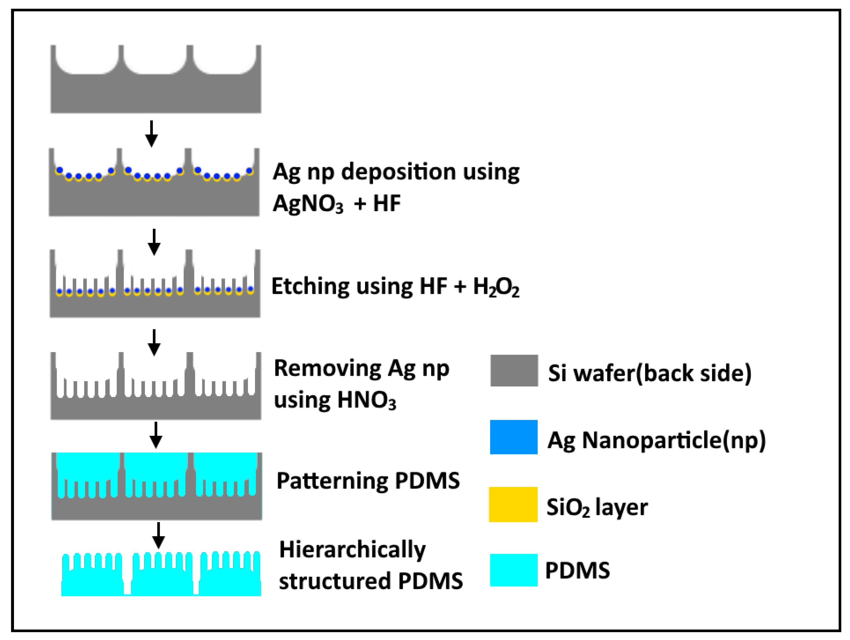
Scheme 1.
Fabrication technique for texturing the lapped unpolished side of a (100) Si wafer and surface patterning of polydimethylsiloxane (PDMS) using the textured Si template. The process involves deposition of a uniform layer of Ag nanoparticles through an electroless deposition using an aqueous electrolyte mixture of AgNO3 and HF followed by treatment with an aqueous solution of HF and H2O2 for 5 s. This resulted in the generation of a hierarchical micro/nano-structure with excellent broadband antireflection property. The textured Si surface can also be used as a template to prepare light trapping structures in PDMS for photovoltaic applications.

Figure 1.
SEM image of the unpolished side of a Si wafer showing regularly distributed square indents; inset shows a higher magnification SEM image.
Figure 1.
SEM image of the unpolished side of a Si wafer showing regularly distributed square indents; inset shows a higher magnification SEM image.

Figure 2.
SEM images of Ag nanoparticles deposited on the unpolished side of the Si wafer for time periods (a) 30 s; (b) 60 s; (c) 120 s (Insets: higher magnification SEM); (d) EDX analysis of Ag nanoparticle deposited (60 s) Si wafer.
Figure 2.
SEM images of Ag nanoparticles deposited on the unpolished side of the Si wafer for time periods (a) 30 s; (b) 60 s; (c) 120 s (Insets: higher magnification SEM); (d) EDX analysis of Ag nanoparticle deposited (60 s) Si wafer.

Figure 3.
Digital photographs of (a) untreated unpolished side of Si wafer; (b) Ag nanoparticles deposited (60 s) on the unpolished side of Si wafer showing a significant change in color; (c) reflectance spectrum of the unpolished side of Si wafer with Ag nanoparticle deposition for different time intervals.

Figure 4.
SEM image of the 5 s etched unpolished side of Si wafer after Ag nanoparticle removal (inset: magnified image showing the formation of nano-structured pits over the Si surface).
Figure 4.
SEM image of the 5 s etched unpolished side of Si wafer after Ag nanoparticle removal (inset: magnified image showing the formation of nano-structured pits over the Si surface).

Figure 5.
(a) Digital photograph of 5 s etched Si wafer (unpolished side) after removal of Ag nanoparticles. (b) Diffused reflectance spectrum of the unpolished side of Si wafer etched for different time intervals varying from 0 s to 20 s. (c) Reflectance spectra from five different regions of the 5 s etched Si wafer. Note: Reflectance spectrum shown is a mean of reflectance measured from five different regions of the wafer marked as #1 (left), #2 (top), #3 (right), #4 (bottom) and #5 (central area).

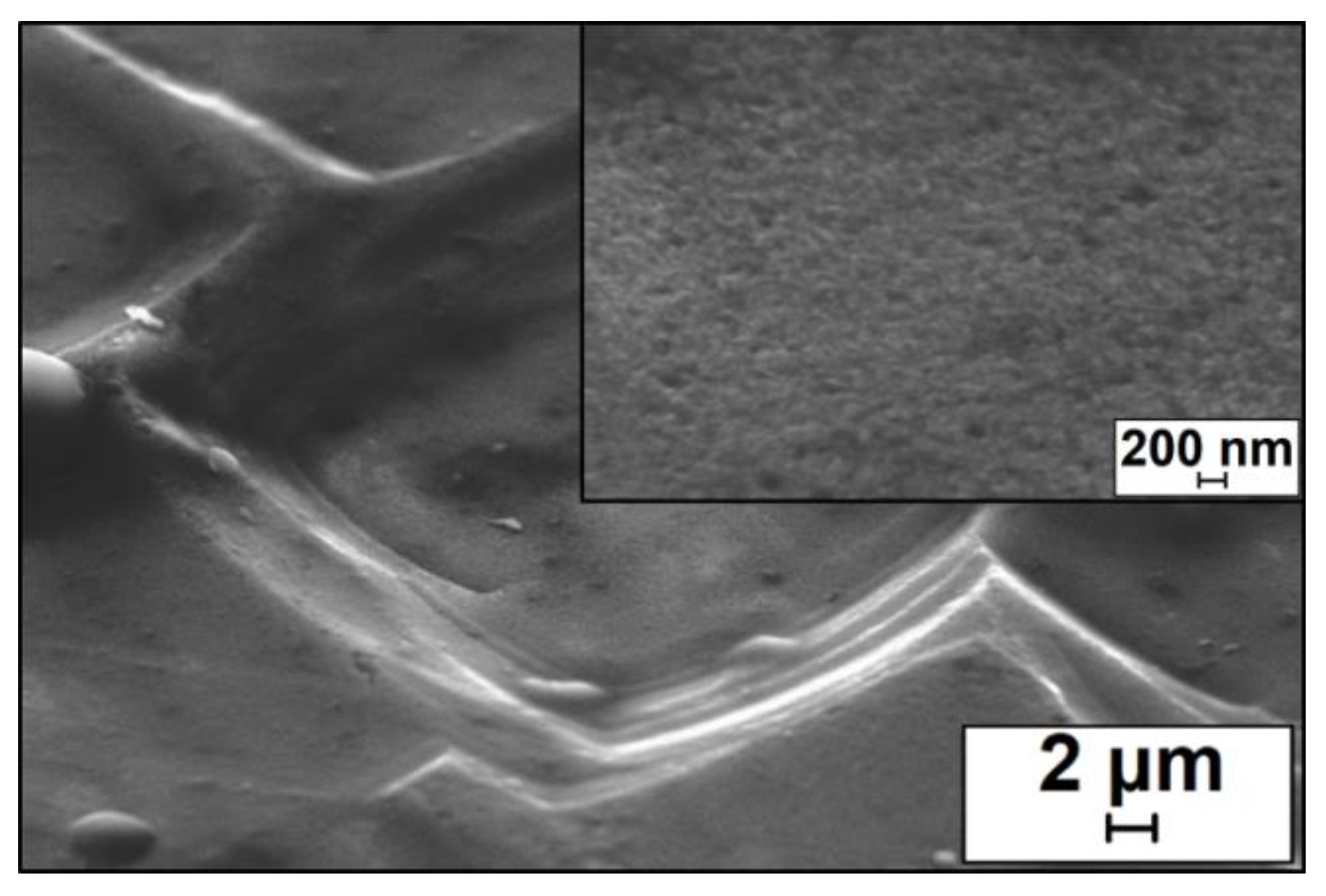
Figure 6.
(a) Digital image of the patterned PDMS membrane (b) SEM image of the hierarchically patterned PDMS; (c) transmittance and reflectance spectrum comparison between planar and patterned PDMS. (d) Variation in surface reflectance across different regions of patterned PDMS; note: Point 1 is the extreme left area, point 2 is the top area, point 3 is the extreme right area, point 4 is the bottom area, and point 5 is the central area.


Table 1.
Surface reflectance comparison on hierarchical structured and inverted micro-pyramidal structured Si.
Table 1.
Surface reflectance comparison on hierarchical structured and inverted micro-pyramidal structured Si.
| Etching Technique | Appearance | Total Etch Time (s) | Bath Temperature (°C) | Average Reflectance (%) | Wavelength Range (nm) | Reference |
|---|---|---|---|---|---|---|
| Anisotropic wet chemical etching + Ag np assisted etching | Hierarchical structure (upright micro-pyramids with nanogrooves) | 1 h 30 min | RT | 4 | 450–2500 | [3] |
| Ag np assisted etching | 1D nano-structures | 50 min | 50°C | 1.46 | 300–600 | [14] |
| Ag ink assisted etching | Vertically standing disordered nano-structures | 13 min | Ag sintering at 170 °C Etching at RT | 1.6 | 300–1100 | [16] |
| Wet chemical etching + Ag np assisted etching | Hierarchical structures (upright micro-pyramids with nano-grooves) | 53 min | RT | 3 | 300–900 | [17] |
| Ni np assisted etching | Inverted micro-pyramid | 1 h | RT | 2.5 | 400–900 | [20] |
| Cu np assisted etching | Inverted micro-pyramid | 8 h | RT | 1 | 300–1000 | [21] |
| Cu np assisted etching | Inverted micro-pyramid | 15 min | 50°C | 5 | 300–1000 | [22,23] |
| Wet chemical etching + Ni np assisted etching | Hierarchical structure (upright micro-pyramids with nano-grooves) | 73 min | RT | 5 | 300–1100 | [28] |
| Ag np assisted etching | Hierarchical structures | 65 s | RT | 2.7 | 300–1400 | [Current work] |
RT: Room temperature; np: Nanoparticle.
Table 2.
Comparative summary of literature reports outlining the recent progress in the realization of patterned PDMS.
Table 2.
Comparative summary of literature reports outlining the recent progress in the realization of patterned PDMS.
| Surface Morphology of Patterned PDMS | Master Template Used and Fabrication Technique | Average Reflectance (%) | Average Transmittance (%) | Reference |
|---|---|---|---|---|
| Micro pyramidal patterned PDMS | Wet anisotropic etching using KOH on Si | 4.7% (300–800 nm) | 95% (300–800 nm) | [36] |
| Nanoscaled inverted moth-eye textured PDMS | Photolithography followed by RIE on Si | 5.5% (350–800 nm) | 94.2% (350–800 nm) | [37] |
| Nanopillar arrayed PDMS membrane | Pre-textured nanohole SU-8 template | - | 94.5% (400–800 nm) | [38] |
| Nanoscaled moth eye featured PDMS stamp | UV-nanoimprint lithography followed by thermoforming process on polystyrene foil | - | 90% (350–850 nm) | [39] |
| Randomly arranged nanoscale moth Eye patterned PDMS | Self-assembly of PFOTHP on glass substrate | - | 94% (400–900 nm) | [40] |
| Hierarchical structure PDMS membrane | Biomimicking using rose petal | 3% (400–1400 nm) | 96% (400–1400 nm) | [42] |
| Hierarchical micro pyramid structured PDMS | Mechanical cutting to pattern inverted micro pyramid on PET film | 5.2% (350–800 nm) | 80% (350–800 nm) | [44] |
| Quantum dot filled nanotextured moth-eye patterned PDMS | Polystyrene beads assisted O2 plasma etching on Si | 8–10% (300–800 nm) | - | [45] |
| Micro-structured PDMS membrane | Metal assisted wet chemical etching | 2.8% (350–1400 nm) | 90% (350–1400 nm) | Present work |
© 2018 by the authors. Licensee MDPI, Basel, Switzerland. This article is an open access article distributed under the terms and conditions of the Creative Commons Attribution (CC BY) license (http://creativecommons.org/licenses/by/4.0/).
Share and Cite
MDPI and ACS Style
Bindra, H.S.; R., J.; Kumeria, T.; Nayak, R. Rapid Processing of Wafer-Scale Anti-Reflecting 3D Hierarchical Structures on Silicon and Its Templation. Materials 2018, 11, 2586. https://doi.org/10.3390/ma11122586
AMA Style
Bindra HS, R. J, Kumeria T, Nayak R. Rapid Processing of Wafer-Scale Anti-Reflecting 3D Hierarchical Structures on Silicon and Its Templation. Materials. 2018; 11(12):2586. https://doi.org/10.3390/ma11122586
Chicago/Turabian StyleBindra, Harsimran Singh, Jaikrishna R., Tushar Kumeria, and Ranu Nayak. 2018. "Rapid Processing of Wafer-Scale Anti-Reflecting 3D Hierarchical Structures on Silicon and Its Templation" Materials 11, no. 12: 2586. https://doi.org/10.3390/ma11122586
Note that from the first issue of 2016, this journal uses article numbers instead of page numbers. See further details here.