Advancements, Challenges and Prospects of Chemical Vapour Pressure at Atmospheric Pressure on Vanadium Dioxide Structures


1
Delta Nano-Engineering Solutions Ltd., Paddock Wood, Kent TN12 6EL, UK
2
Center of Materials Technology and Photonics, School of Applied Technology, Technological Educational Institute of Crete, 710 04 Heraklion, Crete, Greece
3
Institute of Electronic Structure and Laser, Foundation for Research & Technology-Hellas, P.O. Box 1527, Vassilika Vouton, 711 10 Heraklion, Crete, Greece
*
Author to whom correspondence should be addressed.
Materials 2018, 11(3), 384; https://doi.org/10.3390/ma11030384
Submission received: 1 February 2018
/
Revised: 23 February 2018
/
Accepted: 27 February 2018
/
Published: 5 March 2018
(This article belongs to the Special Issue Advances in Chemical Vapor Deposition)
Abstract
:Vanadium (IV) oxide (VO2) layers have received extensive interest for applications in smart windows to batteries and gas sensors due to the multi-phases of the oxide. Among the methods utilized for their growth, chemical vapour deposition is a technology that is proven to be industrially competitive because of its simplicity when performed at atmospheric pressure (APCVD). APCVD’s success has shown that it is possible to create tough and stable materials in which their stoichiometry may be precisely controlled. Initially, we give a brief overview of the basic processes taking place during this procedure. Then, we present recent progress on experimental procedures for isolating different polymorphs of VO2. We outline emerging techniques and processes that yield in optimum characteristics for potentially useful layers. Finally, we discuss the possibility to grow 2D VO2 by APCVD.
1. Chemical Vapour Deposition
1.1. General Information
CVD is a practical method of atomistic or near atomistic deposition having the ability to synthesize well-controlled dimensions and structures at reasonably low temperatures, high purity and in multiple formats such as single layer, multi-layer, composite and finally functional coatings. In its simplest incarnation, CVD encompasses a single precursor gas flowing into a chamber containing the substrate to be coated. Although, there are exceptions, the vapour of the reactive compound, usually an easily volatilized liquid or in some cases a solid, is sublimed directly and transported to the reaction zone by a carrier gas. A thin film is then deposited by chemical reaction or decomposition of the gas mixture on the substrate surface or in its vicinity at a defined temperature.
The precursors used within a variety of CVD techniques can be single source or dual source in origin. Single source precursors contain all the groups/elements required for successive thin film production. On the other hand, dual source precursors involve the interaction between multiple precursors for the synthesis of thin films. In each case, it is vital for production of thin films to deliver the gas phase precursors with a carrier gas. The most common carrier gases are N2, He or Ar, especially when highly reactive or pyrophoric reactants are used and in some cases, reactions entail an energy input from the carrier gas, e.g., H2 or O2 enrichment.
Reactor systems in CVD processes must allow controlled transport of the reactant and diluent gases to the reaction zone, maintain a defined substrate temperature and safely remove the gaseous by-products. These functions should be fulfilled with sufficient control and maximal effectiveness, which requires optimum engineering design and automation. The reactor in which the thin film deposition actually takes place is the essential part of the system and must be designed according to the specific chemical process parameters. To coat layers using Chemical Vapour Deposition at Atmospheric Pressure (APCVD), four basic types can be classified according to their gas flow and operation principles:
- Horizontal tube displacement flow type.
- Rotary vertical batch type.
- Continuous—deposition type using premixed gas flow.
- Continuous—deposition type employing separate gas streams.
1.2. CVD Processes
Any CVD process including APCVD involves the subsequent operations. First, the reacting gas is directed into the reactor. The gas moves towards its thermal equilibrium temperature and composition through gas-phase collisions and reactions. Near-equilibrated species are then transported to the reaction surface, the surface chemical reactions commence and the thin film is formed. The processes are summarized below (Figure 1) [1]:
- Creation of active gaseous reactants.
- Transport of the precursor to the CVD reactor.
- Decomposition of gas phase precursor to remove gaseous by-products and grow reactive intermediates.
- Gaseous reactants transportation onto substrate area.
- Surface diffusion for nucleation and thin film growth.
- Desorption of by-products and mass transport away from active reactive zone.
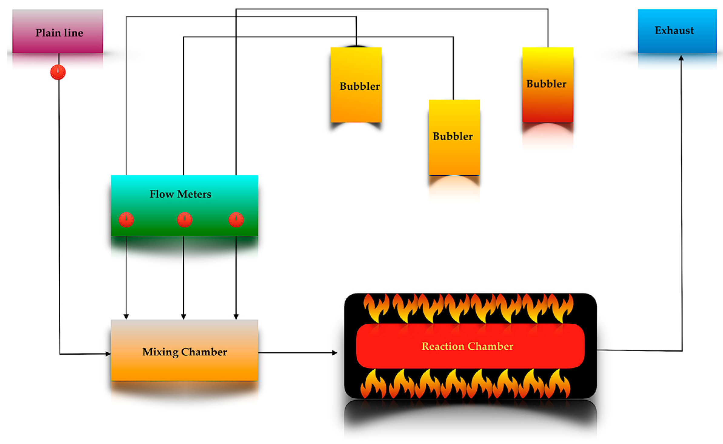
1.3. APCVD
A schematic presentation of the APCVD system is shown in Figure 2. It is designed with no joints in all outlet lines to avoid blocking. A flow of inert gas, usually nitrogen, is passed through the apparatus during all operations. The amount of the precursor delivered into the reactor is calculated from the Equation (1)
where a, is the amount of precursor (mol min−1), VP, is the vapour pressure of precursor at the bubbler’s temperature (mm Hg), F, is the nitrogen flow rate through the bubbler (L min−1) and 24.4, is a constant for the molar volume of an ideal gas at standard temperature and pressure (L mol−1).
In a typical APCVD experiment, once all temperatures are stabilized over time, the N2 is passed through the bubblers and then the precursor gas flow rate is directed into the mixing chamber where the mixture begins in order to be utilized before entering the reaction chamber for the deposition to take place. Once the allotted time is complete, the precursor bubbler is closed. The reactor heater is turned off and the substrate is allowed to cool down under an atmosphere of N2. Ideally, the carrier gas inlet flows should be fully saturated with precursor vapour; this can be achieved with knowledge of the precursor volatility and vapour pressure and then controlled by the carrier gas flow and bubbler temperature using flow meters and heating jackets.
2. Vanadium Oxides
The binary Vanadium-Oxygen phase diagram consists of a large number of phases between V2O3 and VO2 of the form VnO2n−1 commonly known as the Magneli phases [2] that exhibit distinctive electrical and optical properties. The variety of Vanadium-Oxygen stoichiometries emerges from the ability of vanadium atoms to adopt multiple oxidation states, which consequently results in synthetic challenges to control the structure of the materials [3].
More than ten kinds of crystalline phases of VO2 have been reported elsewhere, whereas some examples are monoclinic VO2 (M), tetragonal VO2 (R) and several metastable forms of VO2 (A), VO2 (B) and VO2 (C) [4]. Among these phases, only the rutile VO2 (R/M) phase undergoes a fully reversible metal insulator transition at a critical temperature (Tc) [1], where an abrupt alteration in optical and electronic properties is observed making it ideal for optoelectronic switches [5], memristors [6], artificial neuron networks [7,8] and intelligent window coatings [9,10].
The high temperature phase (T > Tc), has a tetragonal type structure characterized by chains of edge sharing [VO6] octahedral along the c-axis with equidistant vanadium atoms (V-V = 2.88 Å) [11]. While, the low temperature structure involves V4+-V4+ pairing with alternate shorter (0.265 nm) and longer (0.312 nm) V4+-V4+ distances along the a-axis and tilting with respect to the rutile c--axis [11]. At 25 °C, the lattice has unit cell parameters; a = 5.75 Å, b = 4.52 Å, c = 5.38 Å and β = 122.60° [12]. The lattice is the result of the distortion occurring at the high temperature metallic tetragonal phase.
The mechanism of metal insulator transition in VO2 has been investigated through computational, experimental and theoretical studies [13,14,15]. Nevertheless, the mechanism of the transition remains unresolved, since the VO2 phases exhibit diverse lattice structures but have analogous electronic properties.
3. Advancements
There have been numerous studies on the VO2 grown by APCVD since Maruyama and Ikuta utilized vanadium (III) acetylacetonate (V(acac)3) as a single-precursor to deposit polycrystalline pure VO2 films on fused quartz and sapphire single crystals [16]. In this review article, we will focus on the progress taking place during the last four years regarding the control of the processing parameters to isolate the VO2 phases strengthening the functional properties of APCVD VO2 layers.
The growth of amorphous pure and tungsten doped VO2 coatings is possible on SnO2-precoated glass substrates using vanadyl (V) triisopropoxide (VO(OC3H7)3) as single-precursor [9,10,17,18]. It is interesting to note that the presence of tungsten in the lattice of VO2 changed the surface morphology to worm-like (Figure 3) from granular structure [9]. This approach has several advantages including the high vapour pressure of the precursor (i.e., decomposition over time and transport of unknown species are prevented). Additionally, the operations are simplified by removing the commonly necessary oxygen source, which is usually provided either in the form of pure gas or from an extra bubbler through H2O or alcohol. Vanadyl (IV) acetylacetonate (VO(acac)2) along with propanol, ethanol and O2 gas as oxygen sources is accomplished to grow VO2 of different crystalline orientations [19,20]. The a--axis textured monoclinic is enhanced with propanol and ethanol, while the 022-oriented single phase VO2 is obtained with O2 gas possessing grains (a--axis coatings) and agglomeration of grains forming rod-like structures (002-oriented phases). On controlling the oxygen gas flow rate (Figure 4), isolated monoclinic and metastable VO2 phases can also be achieved using VO(acac)2 as vanadium precursor on flexible [21] and SnO2-precoated glass substrates [22].
SnO2 was chosen as a substrate due to the similar crystalline structure with VO2, which can act as a template for the growth of rutile VO2 and promote the crystallinity of the oxide [23].
4. Challenges
A comparative study among VO(acac)2 and VCl4, the most utilized vanadium precursors for APCVD VO2, indicated that the transport rate of VO(acac)2 is lower than VCl4 [24]. This can be handled by increasing the temperature and the N2 flow rate in the bubbler. However, this is not anticipated because the precursor may decompose over time leading to irreproducible delivery rates and the transport of unknown species. On the other hand, VCl4 is highly reactive with H2O resulting in inhomogeneous films [25]. A new approach uses the ethyl acetate (EtAc) as an excellent oxygen precursor resulting in the precise control of the growth rate and porosity of the films after the optimization of VCl4/EtAc system [26]. A route to improve this system involves the combination of X-ray photoelectron spectroscopy (XPS) and X-ray absorption near-edge structure (XANES) to determine the effect of the substrate choice on the VO2 formation for functional properties such as thermochromism [27]. It is then possible to grow VO2 (Figure 5) onto substrates that induce lattice matching (SnO2) or others (F-doped SnO2) that promote a destabilization of V4+ ions and a further increase in V5+ deteriorating the functional properties (Figure 6).
Furthermore, monoclinic VO2 exhibits poor adhesion and is chemically susceptible to attack, restricting the use as solar control coating. In that respect, multi-functional, robust APCVD VO2/SiO2/TiO2 films on glass substrates demonstrates excellent solar modulation properties, high transparency and resistance to abrasion compared to single VO2 films of the same thickness [28].
5. Prospects and Outlook
In the field of APCVD VO2, the altering of the processing parameters and the manipulation of the substrate surface is just starting to be understood. New evolvements in experimental procedures such as the utilization of single vanadium precursor and the oxygen source have addressed APCVD routes in isolating the intrinsic material properties. There are numerous exciting challenges in developing VO2 with functional properties, which expand our understanding of the underlying chemistry and potentially lead to anticipated applications.
Two-dimensional (2D) VO2 can also be possible by APCVD through Computational Fluid Dynamics (CFD) simulations. CFD simulations are performed to evaluate and define the whole experimental process, before, while and after the experimental procedure isolating the intrinsic material properties (Figure 7). CFD results of exhaust and quartz tube presented the simulation procedure regarding the flow rates and the temperature distribution along the boundaries of the metallic parts. The flow rate of N2 was set at 0.1 L min−1 and the temperature in the inner boundaries was at 300 °C. Every aspect of the APCVD process is simulated to approach the optimal characteristics of the oxide in tandem to the surface to be deposited. Prospects in developing the growth of high-quality large-area materials with well-defined sizes, high dispersion and excellent control on layer thickness will then appear. The potential impact is illustrated by considering the exploitation possibilities of the high-performance materials by APCVD to create advanced devices for practical applications.
Acknowledgments
The authors would like to thank Pilkington Glass, UK for the supply of substrates and Aleka Manousaki for the help with the SEM characterization.
Conflicts of Interest
The authors declare no conflict of interest.
References
- Drosos, C.; Vernardou, D. Perspectives of energy materials by APCVD. Sol. Energy Mater. Sol. C 2015, 140, 1–4. [Google Scholar] [CrossRef]
- Chen, X.; Wang, X.; Wang, Z.; Wan, J.; Liu, J.; Qian, Y. An ethylene glycol reduction approach to metastable VO2 nanowire arrays. Nanotechnology 2004, 15, 1685–1687. [Google Scholar] [CrossRef]
- Graf, D.; Schläfer, J.; Garbe, S.; Klein, A.; Mathur, S. Interdepedence of structure, morphology and phase transitions in CVD grown VO2 and V2O3 nanostructures. Chem. Mater. 2017, 29, 5877–5885. [Google Scholar] [CrossRef]
- Wang, S.; Liu, M.; Kong, L.; Long, Y.; Jiang, X.; Yu, A. Recent progress in VO2 smart coatings: Strategies to improve the thermochromic properties. Prog. Mater. Sci. 2016, 81, 1–54. [Google Scholar] [CrossRef]
- Joushaghani, A.; Jeong, J.; Paradis, S.; Alain, D.; Aitchison, J.S.; Poon, J.K.S. Wavelength-size hybrid Si-VO2 waveguide electroabsorption optical switches and photodetectors. Opt. Express 2015, 23, 3657–3688. [Google Scholar] [CrossRef] [PubMed]
- Driscoll, T.; Kim, H.-T.; Chae, B.-G.; Ventra, M.D.; Basov, D.N. Phase-transition driven memristive system. Appl. Phys. Lett. 2009, 95, 043503. [Google Scholar] [CrossRef]
- Pickett, M.D.; Medeiros-Ribeiro, G.; Williams, R.S. A scalable neuristor built with Mott memristors. Nat. Mater. 2013, 12, 114–117. [Google Scholar] [CrossRef] [PubMed]
- Zhou, Y.; Ramanathan, S. Memory and neuromorphic devices. Proc. IEEE 2015, 103, 1289–1310. [Google Scholar] [CrossRef]
- Louloudakis, D.; Vernardou, D.; Spanakis, E.; Suchea, M.; Kenanakis, G.; Pemble, M.E.; Savvakis, C.; Katsarakis, N.; Koudoumas, E.; Kiriakidis, G. Atmospheric pressure chemical vapour deposition of amorphous tungsten doped vanadium dioxide for smart window applications. Adv. Mater. Lett. 2016, 7, 192–196. [Google Scholar] [CrossRef]
- Vernardou, D.; Louloudakis, D.; Spanakis, E.; Katsarakis, N.; Koudoumas, E. Amorphous thermochromic VO2 coatings grown by APCVD at low temperatures. Adv. Mater. Lett. 2015, 6, 660–663. [Google Scholar] [CrossRef]
- Morrison, V.R.; Chatelain, R.P.; Tiwari, K.L.; Hendaoui, A.; Bruhács, A.; Chaker, M.; Siwick, B.J. A photoinduced metal-like phase of monoclinic VO2 revealed by ultrafast electron diffraction. Science 2014, 346, 445–448. [Google Scholar] [CrossRef] [PubMed]
- Eyert, V. The metal-insulator transition of VO2: A band theoretical approach. Ann. Phys. 2002, 11, 650–704. [Google Scholar] [CrossRef]
- Warwick, M.E.A.; Binions, R. Advances in thermochromic vanadium dioxide films. J. Mater. Chem. A 2014, 2, 3275–3292. [Google Scholar] [CrossRef]
- Goodenough, J.B. The two components of the crystallographic transition in VO2. J. Solid State Chem. 1971, 3, 490–500. [Google Scholar] [CrossRef]
- Wentzcovitch, R.M.; Schulz, W.W.; Allen, P.B. VO2: Peierls or Mott-Hubbard? A view from band theory. Phys. Rev. Lett. 1994, 72, 3389–3392. [Google Scholar] [CrossRef] [PubMed]
- Maruyama, T.; Ikuta, Y. Vanadium dioxide thin films prepared by chemical vapour deposition from vanadium(III) acetylacetonate. J. Mater. Sci. 1993, 28, 5073–5078. [Google Scholar] [CrossRef]
- Louloudakis, D.; Vernardou, D.; Spanakis, E.; Katsarakis, N.; Koudoumas, E. Thermochromic vanadium oxide coatings grown by APCVD at low temperatures. Phys. Procedia 2013, 46, 137–141. [Google Scholar] [CrossRef]
- Vernardou, D.; Louloudakis, D.; Spanakis, E.; Katsarakis, N.; Koudoumas, E. Thermochromic amorphous VO2 coatings grown by APCVD using a single-precursor. Sol. Energy Mater. Sol. C 2014, 128, 36–40. [Google Scholar] [CrossRef]
- Vernardou, D.; Bei, A.; Louloudakis, D.; Katsarakis, N.; Koudoumas, E. Oxygen source-oriented control of atmospheric pressure chemical vapour deposition of VO2 for capacitive applications. J. Electrochem. Sci. Eng. 2016, 6, 165–173. [Google Scholar] [CrossRef]
- Louloudakis, D.; Vernardou, D.; Spanakis, E.; Dokianakis, S.; Panagopoulou, M.; Raptis, G.; Aperathitis, E.; Kiriakidis, G.; Katsarakis, N.; Koudoumas, E. Effect of O2 flow rate on the thermochromic performance of VO2 coatings grown by atmospheric pressure CVD. Phys. Status Solidi C 2015, 12, 856–860. [Google Scholar] [CrossRef]
- Vernardou, D.; Louloudakis, D.; Spanakis, E.; Katsarakis, N.; Koudoumas, E. Functional properties of APCVD VO2 layers. Int. J. Thin Films Sci. Technol. 2015, 4, 187–191. [Google Scholar] [CrossRef]
- Vernardou, D.; Apostolopoulou, M.; Louloudakis, D.; Katsarakis, N.; Koudoumas, E. Electrochemical performance of vanadium oxide coatings grown using atmospheric pressure CVD. Chem. Vap. Depos. 2015, 21, 369–374. [Google Scholar] [CrossRef]
- Zhang, Z.; Gao, Y.; Luo, H.; Kang, L.; Chen, Z.; Du, J.; Kanehira, M.; Zhang, Y.; Wang, Z.L. Solution-based fabrication of vanadium dioxide on F:SnO2 substrates with largely enhanced thermochromism and low-emissivity for energy-saving applications. Energy Environ. Sci. 2011, 4, 4290–4297. [Google Scholar] [CrossRef]
- Vernardou, D.; Pemble, M.E.; Sheel, D.W. The growth of thermochromic VO2 films on glass by atmospheric-pressure CVD: A comparative study of precursors, CVD methodology and substrates. Chem. Vap. Depos. 2006, 12, 263–274. [Google Scholar] [CrossRef]
- Béteille, F.; Mazerolles, L.; Livage, J. Microstructure and metal-insulating transition of VO2 thin films. Mater. Res. Bull. 1999, 34, 2177–2184. [Google Scholar] [CrossRef]
- Malarde, D.; Powell, M.J.; Quesada-Cabrera, R.; Wilson, R.L.; Carmalt, C.J.; Samkar, G.; Parkin, I.P.; Palgrave, R.G. Optimized atmospheric-pressure chemical vapour deposition thermochromic VO2 thin films for intelligent window applications. ACS Omega 2017, 2, 1040–1046. [Google Scholar] [CrossRef]
- Powell, M.J.; Godfrey, I.J.; Quesada-Cabrera, R.; Malarde, D.; Teixeira, D.; Emerich, H.; Palgrave, R.G.; Carmalt, C.J.; Parkin, I.P.; Sankar, G. Qualitative XANES and XPS analysis of substrate effects in VO2 thin films: A route to improving chemical vapour deposition synthetic methods? J. Phys. Chem. C. 2017, 121, 20345–20352. [Google Scholar] [CrossRef]
- Powell, M.J.; Quesada-Cabrera, R.; Taylor, A.; Teixeira, D.; Papakonstantinou, I.; Palgrave, R.G.; Sankara, G.; Parkin, I.P. Intelligent multifunctional VO2/SiO2/TiO2 coatings for self-cleaning, energy-saving window panels. Chem. Mater. 2016, 28, 1369–1376. [Google Scholar] [CrossRef]
Figure 1.
Schematic view of CVD (Chemical Vapour Deposition) process [1].
Figure 1.
Schematic view of CVD (Chemical Vapour Deposition) process [1].

Figure 2.
Schematic presentation of an APCVD (Chemical Vapour Deposition at Atmospheric Pressure) system [1].
Figure 2.
Schematic presentation of an APCVD (Chemical Vapour Deposition at Atmospheric Pressure) system [1].

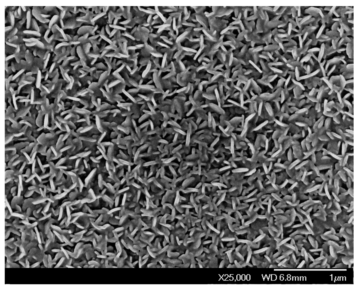
Figure 3.
Field emission-scanning electron microscopy image of the APCVD tungsten doped VO2 coating.
Figure 3.
Field emission-scanning electron microscopy image of the APCVD tungsten doped VO2 coating.

Figure 4.
Field emission-scanning electron microscopy images of APCVD vanadium oxides using oxygen flow rate of 0.4 (a) and 0.8 L min−1 (b).
Figure 4.
Field emission-scanning electron microscopy images of APCVD vanadium oxides using oxygen flow rate of 0.4 (a) and 0.8 L min−1 (b).

Figure 5.
Field emission-scanning electron microscopy image (a) and (b) Raman spectroscopy of APCVD VO2 grown on SnO2-precoated glass substrates. (c) Transmittance spectra below Tc at 25 °C and above Tc at 90 °C over the region of 250–2500 nm to study the thermochromic performance.
Figure 5.
Field emission-scanning electron microscopy image (a) and (b) Raman spectroscopy of APCVD VO2 grown on SnO2-precoated glass substrates. (c) Transmittance spectra below Tc at 25 °C and above Tc at 90 °C over the region of 250–2500 nm to study the thermochromic performance.

Figure 6.
(a) X-ray diffraction of APCVD V2O5 grown on F-doped SnO2. (b) No change in transmittance spectra observed over the region 250–2500 nm below Tc at 25 °C (black colour) and above Tc at 90 °C (red colour).
Figure 6.
(a) X-ray diffraction of APCVD V2O5 grown on F-doped SnO2. (b) No change in transmittance spectra observed over the region 250–2500 nm below Tc at 25 °C (black colour) and above Tc at 90 °C (red colour).

Figure 7.
Simulation of transport species within the components of the APCVD reactor. The simulation showed an increase of the fluid’s velocity from 2.359 × 10⁻³ m s−1 to 3.283 × 10⁻³ m s−1, i.e., an increase of velocity of 39.18% due to temperature change. (Image courtesy of Delta Nano—Engineering Solutions Ltd., London, UK).

© 2018 by the authors. Licensee MDPI, Basel, Switzerland. This article is an open access article distributed under the terms and conditions of the Creative Commons Attribution (CC BY) license (http://creativecommons.org/licenses/by/4.0/).
Share and Cite
MDPI and ACS Style
Drosos, C.; Vernardou, D. Advancements, Challenges and Prospects of Chemical Vapour Pressure at Atmospheric Pressure on Vanadium Dioxide Structures. Materials 2018, 11, 384. https://doi.org/10.3390/ma11030384
AMA Style
Drosos C, Vernardou D. Advancements, Challenges and Prospects of Chemical Vapour Pressure at Atmospheric Pressure on Vanadium Dioxide Structures. Materials. 2018; 11(3):384. https://doi.org/10.3390/ma11030384
Chicago/Turabian StyleDrosos, Charalampos, and Dimitra Vernardou. 2018. "Advancements, Challenges and Prospects of Chemical Vapour Pressure at Atmospheric Pressure on Vanadium Dioxide Structures" Materials 11, no. 3: 384. https://doi.org/10.3390/ma11030384
Note that from the first issue of 2016, this journal uses article numbers instead of page numbers. See further details here.