
Atomic Layer Deposition of Silicon Nitride Thin Films: A Review of Recent Progress, Challenges, and Outlooks

 ,
,
Abstract
:1. Introduction
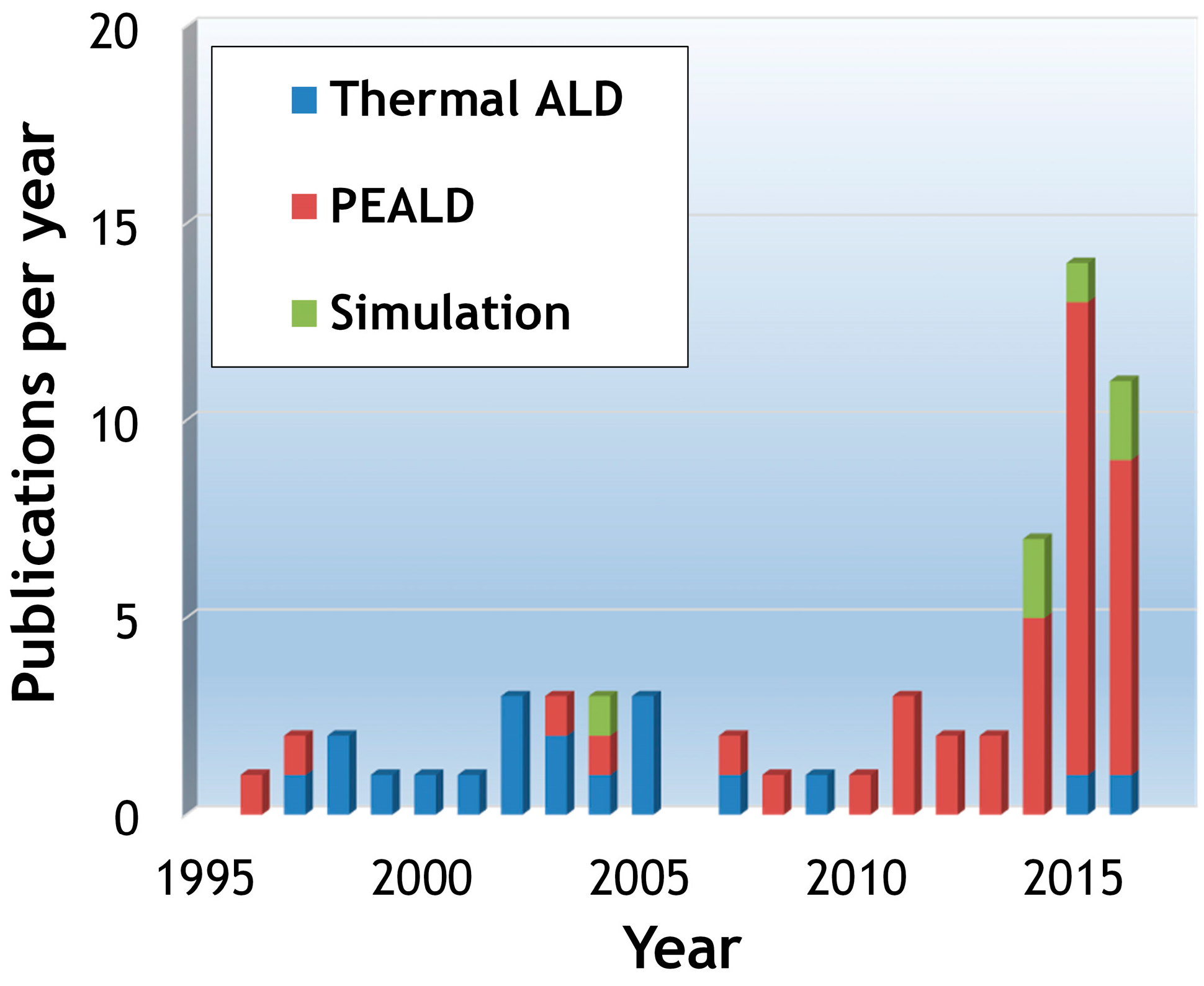
2. Current Research Progress
2.1. Growth of Silicon Nitride (SiNx) Thin Films via Atomic Layer Deposition (ALD)
2.1.1. Thermal ALD
2.1.2. Plasma-Enhanced ALD
2.2. Applications of SiNx ALD
2.2.1. Gate Spacer
- Good conformalityA gate spacer must be conformal with minimal wafer loading effects, which ensures that spacer thickness is homogeneously distributed across the wafer. Additionally, the spacer shape is a critical factor that will affect the profile of implanted dopants and will, therefore, define the p-n junction. A steeper sidewall will result in a more well-defined source/drain region [5].
- Good etch resistance
- Low deposition temperature
2.2.2. Gate Dielectric
2.2.3. Encapsulation Layer
2.2.4. Deposition of Composite Films
2.2.5. Stressor
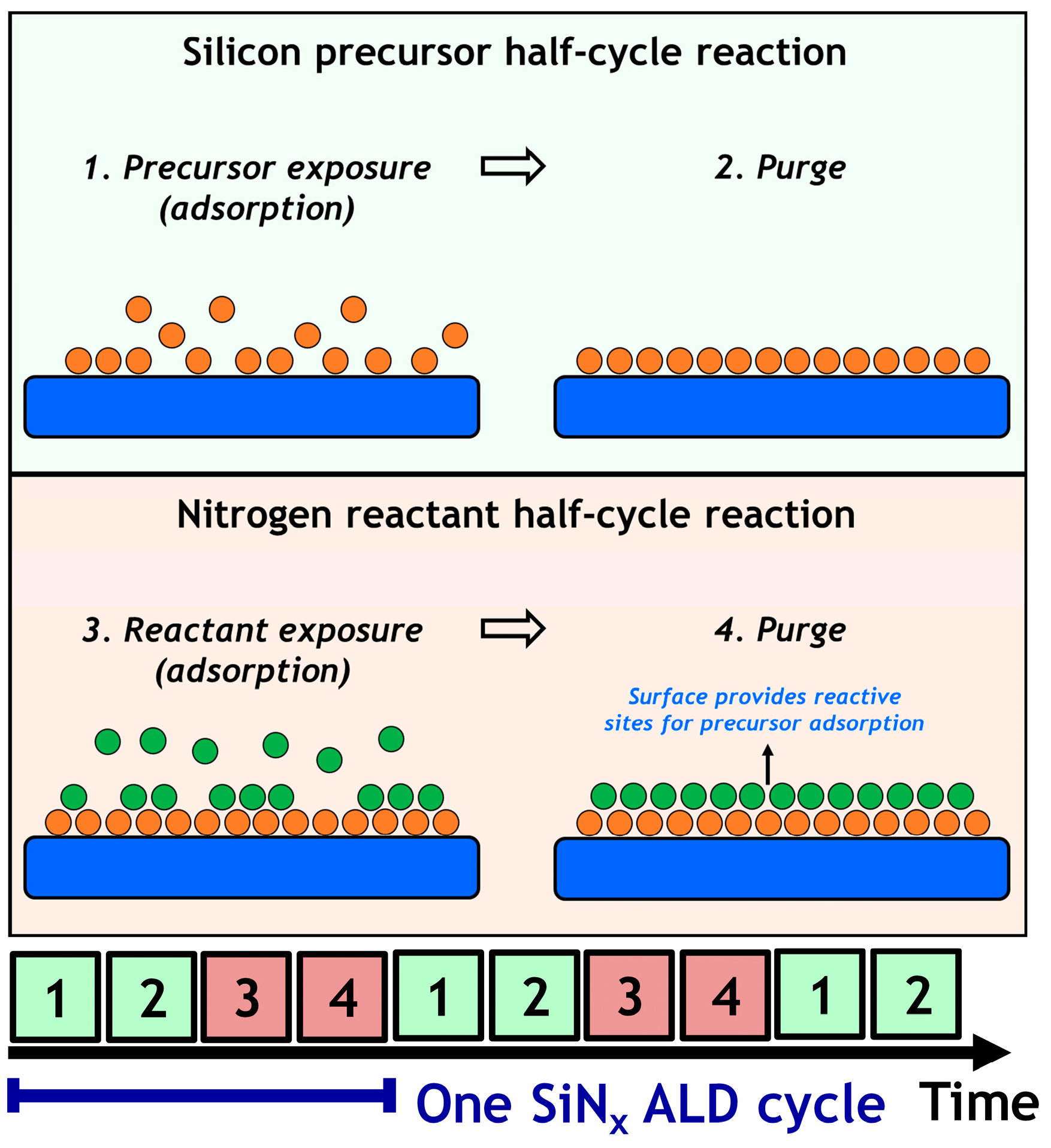
2.3. A Highlighted Topic: The Surface Reactions of SiNx ALD
3. Challenges of SiNx ALD
3.1. Thermal ALD
3.1.1. Limitation of the Deposition Temperature
3.1.2. Excess Precursor Dosage and Dosing Time
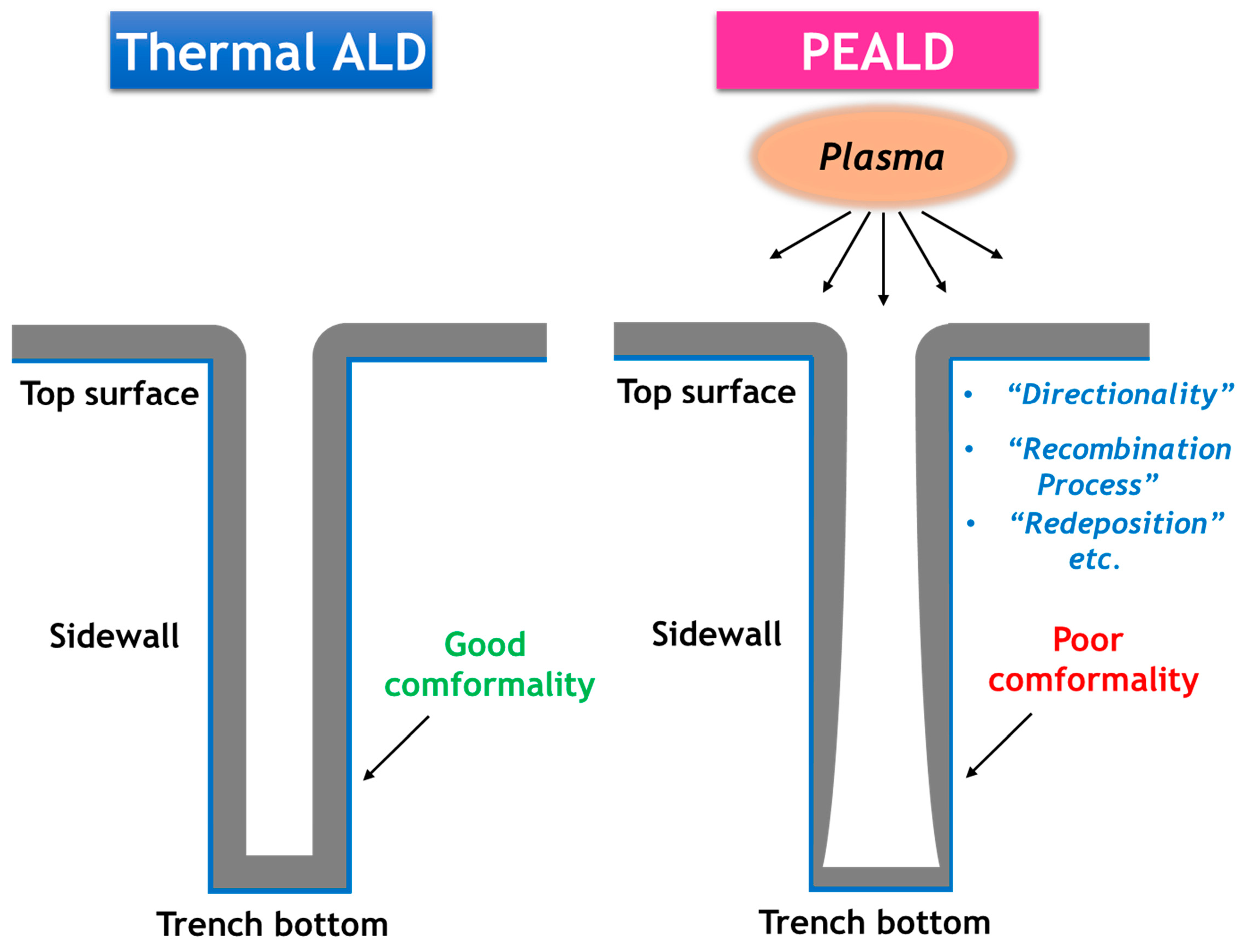
3.2. Plasma-Enhanced ALD
Degradation of the Conformality
3.3. Other Common Challenges
3.3.1. Chlorine Impurities and Byproducts from the Chlorine-Containing Precursors
3.3.2. Substrate Sensitivity
4. Conclusions and Outlooks
Acknowledgments
Conflicts of Interest
References
- Kern, W.; Schuegraf, K.K. Deposition Technologies and Applications: Introduction and Overview. In Handbook of Thin Film Deposition Processes and Techniques, 2nd ed.; Seshan, K., Ed.; William Andrew Publishing: Norwich, NY, USA, 2001; pp. 11–43. [Google Scholar]
- Jang, W.; Jeon, H.; Song, H.; Kim, H.; Park, J.; Kim, H.; Jeon, H. The effect of plasma power on the properties of low-temperature silicon nitride deposited by RPALD for a gate spacer. Phys. Status Solidi 2015, 212, 2785–2790. [Google Scholar] [CrossRef]
- Xia, L.-Q.; Chang, M. Chemical Vapor Deposition. In Handbook of Semiconductor Manufacturing Technology, 2nd ed.; Doering, R., Nishi, Y., Eds.; CRC Press: Boca Raton, FL, USA, 2007; pp. 13-1–13-87. [Google Scholar]
- King, S.W. Plasma enhanced atomic layer deposition of SiNx:H and SiO2. J. Vac. Sci. Technol. A 2011, 29, 041501. [Google Scholar] [CrossRef]
- Triyoso, D.H.; Hempel, K.; Ohsiek, S.; Jaschke, V.; Shu, J.; Mutas, S.; Dittmar, K.; Schaeffer, J.; Utess, D.; Lenski, M. Evaluation of low temperature silicon nitride spacer for high-k metal gate integration. ECS J. Solid State Sci. Technol. 2013, 2, N222–N227. [Google Scholar] [CrossRef]
- George, S.M. Atomic layer deposition: An overview. Chem. Rev. 2010, 110, 111–131. [Google Scholar] [CrossRef] [PubMed]
- Qin, X.; Cheng, L.; McDonnell, S.; Azcatl, A.; Zhu, H.; Kim, J.; Wallace, R.M. A comparative study of atomic layer deposition of Al2O3 and HfO2 on AlGaN/GaN. J. Mater. Sci. Mater. Electron. 2015, 26, 4638–4643. [Google Scholar] [CrossRef]
- Lucero, A.T.; Byun, Y.-C.; Qin, X.; Cheng, L.; Kim, H.; Wallace, R.M.; Kim, J. In-situ XPS study of ALD ZnO passivation of p-In0.53Ga0.47As. Electron. Mater. Lett. 2015, 11, 769–774. [Google Scholar] [CrossRef]
- Lucero, A.T.; Byun, Y.-C.; Qin, X.; Cheng, L.; Kim, H.; Wallace, R.M.; Kim, J. Formation of a ZnO/ZnS interface passivation layer on (NH4)2S treated In0.53Ga0.47As: Electrical and in-situ X-ray photoelectron spectroscopy characterization. Jpn. J. Appl. Phys. 2016, 55, 08PC02. [Google Scholar] [CrossRef]
- Leskelä, M.; Ritala, M. Atomic layer deposition (ALD): From precursors to thin film structures. Thin Solid Films 2002, 409, 138–146. [Google Scholar] [CrossRef]
- Leskelä, M.; Ritala, M. Atomic layer deposition chemistry: Recent developments and future challenges. Angew. Chem. Int. Ed. 2003, 42, 5548–5554. [Google Scholar] [CrossRef] [PubMed]
- Puurunen, R.L. Surface chemistry of atomic layer deposition: A case study for the trimethylaluminum/water process. J. Appl. Phys. 2005, 97, 121301. [Google Scholar] [CrossRef]
- Kim, J.; Kim, T.W. Initial surface reactions of atomic layer deposition. JOM 2009, 61, 17–22. [Google Scholar] [CrossRef]
- Profijt, H.B.; Potts, S.E.; van de Sanden, M.C.M.; Kessels, W.M.M. Plasma-assisted atomic layer deposition: Basics, opportunities, and challenges. J. Vacuum Sci. Technol. A 2011, 29, 050801. [Google Scholar] [CrossRef]
- Hyungjun, K.; II-Kwon, O. Review of plasma-enhanced atomic layer deposition: Technical enabler of nanoscale device fabrication. Jpn. J. Appl. Phys. 2014, 53, 03DA01. [Google Scholar]
- Goto, H.; Shibahara, K.; Yokoyama, S. Atomic layer controlled deposition of silicon nitride with self-limiting mechanism. Appl. Phys. Lett. 1996, 68, 3257–3259. [Google Scholar] [CrossRef]
- Morishita, S.; Sugahara, S.; Matsumura, M. Atomic-layer chemical-vapor-deposition of silicon-nitride. Appl. Surf. Sci. 1997, 112, 198–204. [Google Scholar] [CrossRef]
- Alvarez, D.; Spiegelman, J.; Heinlein, E.; Holmes, R.; Ramos, C.; Leo, M.; Webb, S. Novel oxidants and sources of nitrogen for atomic layer deposition. ECS Trans. 2016, 72, 243–248. [Google Scholar] [CrossRef]
- Klaus, J.W.; Ott, A.W.; Dillon, A.C.; George, S.M. Atomic layer controlled growth of Si3N4 films using sequential surface reactions. Surf. Sci. 1998, 418, L14–L19. [Google Scholar] [CrossRef]
- Nakajima, A.; Yoshimoto, T.; Kidera, T.; Obata, K.; Yokoyama, S.; Sunami, H.; Hirose, M. Atomic-layer-deposited silicon-nitride/SiO2 stacked gate dielectrics for highly reliable p-metal-oxide-semiconductor field-effect transistors. Appl. Phys. Lett. 2000, 77, 2855–2857. [Google Scholar] [CrossRef]
- Nakajima, A.; Yoshimoto, T.; Kidera, T.; Yokoyama, S. Low-temperature formation of silicon nitride gate dielectrics by atomic-layer deposition. Appl. Phys. Lett. 2001, 79, 665–667. [Google Scholar] [CrossRef]
- Nakajima, A.; Khosru, Q.D.M.; Yoshimoto, T.; Kidera, T.; Yokoyama, S. NH3-annealed atomic-layer-deposited silicon nitride as a high-k gate dielectric with high reliability. Appl. Phys. Lett. 2002, 80, 1252–1254. [Google Scholar] [CrossRef]
- Nakajima, A.; Khosru, Q.D.M.; Yoshimoto, T.; Kidera, T.; Yokoyama, S. Low-temperature formation of highly reliable silicon-nitride gate dielectrics with suppressed soft-breakdown phenomena for advanced complementary metal-oxide-semiconductor technology. J. Vacuum Sci. Technol. B 2002, 20, 1406–1409. [Google Scholar] [CrossRef]
- Nakajima, A.; Khosru, Q.D.M.; Yoshimoto, T.; Yokoyama, S. Atomic-layer-deposited silicon-nitride/SiO2 stack—A highly potential gate dielectrics for advanced CMOS technology. Microelectron. Reliabil. 2002, 42, 1823–1835. [Google Scholar] [CrossRef]
- Nakajima, A.; Ishii, H.; Kitade, T.; Yokoyama, S. Atomic-layer-deposited ultrathin Si-nitride gate dielectrics—A better choice for sub-tunneling gate dielectrics. In Proceedings of the 2003 IEEE International Electron Devices Meeting, IEDM ‘03 Technical Digest, Washington, DC, USA, 8–10 December 2003; pp. 28.22.21–28.22.24.
- Nakajima, A.; Khosru, Q.D.M.; Yoshimoto, T.; Kasai, T.; Yokoyama, S. High quality atomic-layer-deposited ultrathin Si-nitride gate dielectrics with low density of interface and bulk traps. Appl. Phys. Lett. 2003, 83, 335–337. [Google Scholar] [CrossRef]
- Lee, W.-J.; Lee, J.-H.; Park, C.O.; Lee, Y.-S.; Shin, S.-J.; Rha, S.-K. A comparative study on the Si precursors for the atomic layer deposition of silicon nitride thin films. J. Korean Phys. Soc. 2004, 45, 1352–1355. [Google Scholar]
- Zhu, S.; Nakajima, A. Atomic layer deposition of HfO2 and Si nitride on Ge substrates. Jpn J. Appl. Phys. 2007, 46, 7699–7701. [Google Scholar] [CrossRef]
- Yokoyama, S.; Ikeda, N.; Kajikawa, K.; Nakashima, Y. Atomic-layer selective deposition of silicon nitride on hydrogen-terminated Si surfaces. Appl. Surf. Sci. 1998, 130–132, 352–356. [Google Scholar] [CrossRef]
- Hansch, W.; Nakajima, A.; Yokoyama, S. Characterization of silicon/oxide/nitride layers by X-ray photoelectron spectroscopy. Appl. Phys. Lett. 1999, 75, 1535–1537. [Google Scholar] [CrossRef]
- Lee, W.-J.; Kim, U.-J.; Han, C.-H.; Chun, M.-H.; Rha, S.-K.; Lee, Y.-S. Characteristics of silicon nitride thin films prepared by using alternating exposures of Si2Cl6 and NH3. J. Korean Phys. Soc. 2005, 47, S598–S602. [Google Scholar]
- Park, K.; Yun, W.-D.; Choi, B.-J.; Kim, H.-D.; Lee, W.-J.; Rha, S.-K.; Park, C.O. Growth studies and characterization of silicon nitride thin films deposited by alternating exposures to Si2Cl6 and NH3. Thin Solid Films 2009, 517, 3975–3978. [Google Scholar] [CrossRef]
- Riedel, S.; Sundqvist, J.; Gumprecht, T. Low temperature deposition of silicon nitride using Si3Cl8. Thin Solid Films 2015, 577, 114–118. [Google Scholar] [CrossRef]
- Yusup, L.L.; Park, J.-M.; Noh, Y.-H.; Kim, S.-J.; Lee, W.-J.; Park, S.; Kwon, Y.-K. Reactivity of different surface sites with silicon chlorides during atomic layer deposition of silicon nitride. RSC Adv. 2016, 6, 68515–68524. [Google Scholar] [CrossRef]
- Matsumura, H. Silicon nitride produced by catalytic chemical vapor deposition method. J. Appl. Phys. 1989, 66, 3612–3617. [Google Scholar] [CrossRef]
- Mahan, A.H. An update on silicon deposition performed by hot wire CVD. Thin Solid Films 2006, 501, 3–7. [Google Scholar] [CrossRef]
- Verlaan, V.; Houweling, Z.S.; van der Werf, C.H.M.; Romijn, I.G.; Weeber, A.W.; Goldbach, H.D.; Schropp, R.E.I. Deposition of device quality silicon nitride with ultra high deposition rate (>7 nm/s) using hot-wire CVD. Thin Solid Films 2008, 516, 533–536. [Google Scholar] [CrossRef]
- Alpuim, P.; Gonçalves, L.M.; Marins, E.S.; Viseu, T.M.R.; Ferdov, S.; Bourée, J.E. Deposition of silicon nitride thin films by hot-wire CVD at 100 °C and 250 °C. Thin Solid Films 2009, 517, 3503–3506. [Google Scholar] [CrossRef]
- Potts, S.E.; Kessels, W.M.M. Energy-enhanced atomic layer deposition for more process and precursor versatility. Coord. Chem. Rev. 2013, 257, 3254–3270. [Google Scholar] [CrossRef]
- Suh, S.; Ryu, S.W.; Cho, S.; Kim, J.-R.; Kim, S.; Hwang, C.S.; Kim, H.J. Low-temperature SiON films deposited by plasma-enhanced atomic layer deposition method using activated silicon precursor. J. Sci. Technol. A Vac. Surf. Films 2016, 34, 01A136. [Google Scholar] [CrossRef]
- Park, T.J.; Sivasubramani, P.; Coss, B.E.; Kim, H.-C.; Lee, B.; Wallace, R.M.; Kim, J.; Rousseau, M.; Liu, X.; Li, H.; et al. Effects of O3 and H2O oxidants on C and N-related impurities in atomic-layer-deposited La2O3 films observed by in situ x-ray photoelectron spectroscopy. Appl. Phys. Lett. 2010, 97, 092904. [Google Scholar] [CrossRef]
- Koehler, F.; Triyoso, D.H.; Hussain, I.; Mutas, S.; Bernhardt, H. Atomic layer deposition of SiN for spacer applications in high-end logic devices. IOP Conf. Ser. Mater. Sci. Eng. 2012, 41, 012006. [Google Scholar] [CrossRef]
- Koehler, F.; Triyoso, D.H.; Hussain, I.; Antonioli, B.; Hempel, K. Challenges in spacer process development for leading-edge high-k metal gate technology. Phys. Status Solidi 2014, 11, 73–76. [Google Scholar] [CrossRef]
- Yokoyama, S.; Goto, H.; Miyamoto, T.; Ikeda, N.; Shibahara, K. Atomic layer controlled deposition of silicon nitride and in situ growth observation by infrared reflection absorption spectroscopy. Appl. Surf. Sci. 1997, 112, 75–81. [Google Scholar] [CrossRef]
- Ando, T.; Ohta, Y.; Ashihara, H.; Imai, T. A silicon nitride MIM capacitor for analog/mixed-signal integrated circuit using manufacturable atomic layer deposition equipment. ECS Trans. 2007, 11, 55–60. [Google Scholar]
- Yang, J.-H.; Park, J.-E.; Lee, J.-W.; Chu, K.-S.; Ku, J.-H.; Park, M.-H.; Lee, N.-I.; Kang, H.-S.; Oh, M.-H.; Lee, J.-H.; et al. Ultimate solution for low thermal budget gate spacer and etch stopper to retard short channel effect in sub-90 nm devices. In Proceedings of the 2003 Symposium on VLSI Technology, Digest of Technical Papers, Kyoto, Japan, 10–12 June 2003; pp. 55–56.
- Nagata, K.; Nagasaka, M.; Yamaguchi, T.; Ogura, A.; Oji, H.; Son, J.-Y.; Hirosawa, I.; Watanabe, Y.; Hirota, Y. Evaluation of stress induced by plasma assisted ALD SiN film. ECS Trans. 2013, 53, 51–56. [Google Scholar] [CrossRef]
- Provine, J.; Schindler, P.; Kim, Y.; Walch, S.P.; Kim, H.J.; Kim, K.-H.; Prinz, F.B. Correlation of film density and wet etch rate in hydrofluoric acid of plasma enhanced atomic layer deposited silicon nitride. AIP Adv. 2016, 6, 065012. [Google Scholar] [CrossRef]
- Ovanesyan, R.A.; Hausmann, D.M.; Agarwal, S. Low-temperature conformal atomic layer deposition of SiNx films using Si2Cl6 and NH3 plasma. ACS Appl. Mater. Interfaces 2015, 7, 10806–10813. [Google Scholar] [CrossRef] [PubMed]
- Li, W.-M. Towards commercialization of AlN and SiNx thin film materials via thermal and plasma-enhanced ALD. In Proceedings of the 15th International Conference on Atomic Layer Deposition, Portland, OR, USA, 28 June–1 July 2015.
- Fang, Q.; Hodson, C. Silicon nitride and silicon oxide thin films by plasma ALD. In Proceedings of the 8th International Conference on Atomic Layer Deposition, Bruges, Belgium, 29 June–2 July 2008.
- Kim, Y.; Provine, J.; Walch, S.P.; Park, J.; Phuthong, W.; Dadlani, A.L.; Kim, H.-J.; Schindler, P.; Kim, K.; Prinz, F.B. Plasma-enhanced atomic layer deposition of SiN–AlN composites for ultra low wet etch rates in hydrofluoric acid. ACS Appl. Mater. Interfaces 2016, 8, 17599–17605. [Google Scholar] [CrossRef] [PubMed]
- Knoops, H.C.M.; Braeken, E.M.J.; de Peuter, K.; Potts, S.E.; Haukka, S.; Pore, V.; Kessels, W.M.M. Atomic layer deposition of silicon nitride from bis(tert-butylamino)silane and N2 plasma. ACS Appl. Mater. Interfaces 2015, 7, 19857–19862. [Google Scholar] [CrossRef] [PubMed]
- Ande, C.K.; Knoops, H.C.M.; de Peuter, K.; van Drunen, M.; Elliott, S.D.; Kessels, W.M.M. Role of surface termination in atomic layer deposition of silicon nitride. J. Phys. Chem. Lett. 2015, 6, 3610–3614. [Google Scholar] [CrossRef] [PubMed]
- Andringa, A.-M.; Perrotta, A.; de Peuter, K.; Knoops, H.C.M.; Kessels, W.M.M.; Creatore, M. Low-temperature plasma-assisted atomic layer deposition of silicon nitride moisture permeation barrier layers. ACS Appl. Mater. Interfaces 2015, 7, 22525–22532. [Google Scholar] [CrossRef] [PubMed]
- Knoops, H.C.M.; de Peuter, K.; Kessels, W.M.M. Redeposition in plasma-assisted atomic layer deposition: Silicon nitride film quality ruled by the gas residence time. Appl. Phys. Lett. 2015, 107, 014102. [Google Scholar] [CrossRef]
- Park, J.M.; Jang, S.J.; Yusup, L.L.; Lee, W.J.; Lee, S.I. Plasma-enhanced atomic layer deposition of silicon nitride using a novel silylamine precursor. ACS Appl. Mater. Interfaces 2016, 8, 20865–20871. [Google Scholar] [CrossRef] [PubMed]
- Eom, T.-K.; Kim, S.-H.; Kang, D.-H.; Kim, H. Characteristics of plasma-enhanced atomic layer deposited RuSiN as a diffusion barrier against Cu. J. Electrochem. Soc. 2011, 158, D657–D663. [Google Scholar] [CrossRef]
- Eom, T.-K.; Kim, S.-H.; Park, K.-S.; Kim, S.; Kim, H. Formation of nano-crystalline Ru-based ternary thin films by plasma-enhanced atomic layer deposition. Electrochem. Solid State Lett. 2011, 14, D10–D12. [Google Scholar] [CrossRef]
- Karbasian, G.; Orlov, A.O.; Mukasyan, A.S.; Snider, G.L. Single-electron transistors featuring silicon nitride tunnel barriers prepared by atomic layer deposition. In Proceedings of the 2016 Joint International EUROSOI Workshop and International Conference on Ultimate Integration on Silicon (EUROSOI-ULIS), Wien, Vienna, Austria, 25–27 January 2016; pp. 32–35.
- King, S. Plasma enhanced atomic layer deposition of SiN:H using N2 and Silane. ECS Trans. 2010, 33, 365–373. [Google Scholar]
- Park, J.-S.; Kang, S.-W.; Kim, H. Growth mechanism and diffusion barrier property of plasma-enhanced atomic layer deposition Ti–Si–N thin films. J. Vacuum Sci. Technol. B 2006, 24, 1327–1332. [Google Scholar] [CrossRef]
- Jang, W.; Jeon, H.; Kang, C.; Song, H.; Park, J.; Kim, H.; Seo, H.; Leskela, M.; Jeon, H. Temperature dependence of silicon nitride deposited by remote plasma atomic layer deposition. Phys. Status Solidi 2014, 211, 2166–2171. [Google Scholar] [CrossRef]
- Jang, W.; Jeon, H.; Song, H.; Park, J.; Kim, H.; Kim, H.; Jeon, H. Low temperature silicon nitride ALD. In Proceedings of the 15th International Conference on Atomic Layer Deposition, Portland, OR, USA, 28 June–1 July 2015.
- Weeks, S.; Nowling, G.; Fuchigami, N.; Bowes, M.; Littau, K. Plasma enhanced atomic layer deposition of silicon nitride using neopentasilane. J. Vac. Sci. Technol. A Vac. Surf. Films 2016, 34, 01A140. [Google Scholar] [CrossRef]
- Gumpher, J.; Bather, W.; Mehta, N.; Wedel, D. Characterization of low-temperature silicon nitride LPCVD from bis (tertiary-butylamino) silane and ammonia. J. Electrochem. Soc. 2004, 151, G353–G359. [Google Scholar] [CrossRef]
- Bosch, R.H.E.C.; Cornelissen, L.E.; Knoops, H.C.M.; Kessels, W.M.M. Atomic layer deposition of silicon nitride from bis(tertiary-butyl-amino)silane and N2 plasma studied by in situ gas phase and surface infrared spectroscopy. Chem. Mater. 2016, 28, 5864–5871. [Google Scholar] [CrossRef]
- Chow, R.; Lanford, W.A.; Wang, K.M.; Rosler, R.S. Hydrogen content of a variety of plasma-deposited silicon nitrides. J. Appl. Phys. 1982, 53, 5630–5633. [Google Scholar] [CrossRef]
- Claassen, W.; Valkenburg, W.; Habraken, F.; Tamminga, Y. Characterization of plasma silicon nitride layers. J. Electrochem. Soc. 1983, 130, 2419–2423. [Google Scholar] [CrossRef]
- Manabe, Y.; Mitsuyu, T. Silicon nitride thin films prepared by the electron cyclotron resonance plasma chemical vapor deposition method. J. Appl. Phys. 1989, 66, 2475–2480. [Google Scholar] [CrossRef]
- Mistry, K.; Allen, C.; Auth, C.; Beattie, B.; Bergstrom, D.; Bost, M.; Brazier, M.; Buehler, M.; Cappellani, A.; Chau, R.; et al. A 45nm logic technology with high-k+metal gate transistors, strained silicon, 9 Cu interconnect layers, 193nm dry patterning, and 100% Pb-free packaging. In Proceedings of the 2007 IEEE International Electron Devices Meeting, Washington, DC, USA, 10–12 December 2007; pp. 247–250.
- Wilk, G.D.; Wallace, R.M.; Anthony, J.M. High-κ gate dielectrics: Current status and materials properties considerations. J. Appl. Phys. 2001, 89, 5243–5275. [Google Scholar] [CrossRef]
- Lee, B.; Choi, K.J.; Hande, A.; Kim, M.J.; Wallace, R.M.; Kim, J.; Senzaki, Y.; Shenai, D.; Li, H.; Rousseau, M.; et al. A novel thermally-stable zirconium amidinate ALD precursor for ZrO2 thin films. Microelectron. Eng. 2009, 86, 272–276. [Google Scholar] [CrossRef]
- Lee, B.; Park, T.J.; Hande, A.; Kim, M.J.; Wallace, R.M.; Kim, J.; Liu, X.; Yi, J.H.; Li, H.; Rousseau, M.; et al. Electrical properties of atomic-layer-deposited La2O3 films using a novel La formamidinate precursor and ozone. Microelectron. Eng. 2009, 86, 1658–1661. [Google Scholar] [CrossRef]
- McDonnell, S.; Dong, H.; Hawkins, J.M.; Brennan, B.; Milojevic, M.; Aguirre-Tostado, F.S.; Zhernokletov, D.M.; Hinkle, C.L.; Kim, J.; Wallace, R.M. Interfacial oxide re-growth in thin film metal oxide III–V semiconductor systems. Appl. Phys. Lett. 2012, 100, 141606. [Google Scholar] [CrossRef]
- Triyoso, D.H.; Jaschke, V.; Shu, J.; Mutas, S.; Hempel, K.; Schaeffer, J.K.; Lenski, M. Robust PEALD SiN spacer for gate first high-k metal gate integration. In Proceedings of the 2012 IEEE International Conference on IC Design & Technology (ICICDT), Austin, TX, USA, 30 May–1 June 2012; pp. 1–4.
- Heyns, M.; Tsai, W. Ultimate scaling of CMOS logic devices with Ge and III-V materials. MRS Bull. 2009, 34, 485–492. [Google Scholar] [CrossRef]
- Djara, V.; Deshpande, V.; Sousa, M.; Caimi, D.; Czornomaz, L.; Fompeyrine, J. CMOS-compatible replacement metal gate InGaAs-OI FinFET with Ion = 156 µA/µm at Vdd = 0.5 V and Ioff = 100 nA/µm. IEEE Electron. Device Lett. 2016, 37, 169–172. [Google Scholar] [CrossRef]
- Hong, S.H.; Jang, J.H.; Park, T.J.; Jeong, D.S.; Kim, M.; Hwang, C.S.; Won, J.Y. Improvement of the current-voltage characteristics of a tunneling dielectric by adopting a Si3N4/SiO2/Si3N4 multilayer for flash memory application. Appl. Phys. Lett. 2005, 87, 152106. [Google Scholar] [CrossRef]
- Hong, S.H.; Jang, J.H.; Park, T.J.; Jeong, D.S.; Kim, M.; Hwang, C.S. Improvement of the current-voltage characteristics of a tunneling dielectric by barrier engineering by adopting an atomic-layer-deposited SiN layer for flash memory applications. In Proceedings of the 2005 35th European Solid-State Device Research Conference (ESSDERC 2005), Grenoble, France, 12–16 September 2005; pp. 517–520.
- Oka, T.; Nozawa, T. AlGaN/GaN recessed MIS-gate HFET with high-threshold-voltage normally-off operation for power electronics applications. IEEE Electron. Device Lett. 2008, 29, 668–670. [Google Scholar] [CrossRef]
- Ishida, M.; Uemoto, Y.; Ueda, T.; Tanaka, T.; Ueda, D. GaN power switching devices. In Proceedings of the 2010 International Power Electronics Conference (IPEC), Sapporo, Japan, 21–24 June 2010; pp. 1014–1017.
- Chen, K.J.; Zhou, C. Enhancement-mode AlGaN/GaN HEMT and MIS-HEMT technology. Phys. Status Solidi 2011, 208, 434–438. [Google Scholar] [CrossRef]
- Brennan, B.; Qin, X.; Dong, H.; Kim, J.; Wallace, R.M. In situ atomic layer deposition half cycle study of Al2O3 growth on AlGaN. Appl. Phys. Lett. 2012, 101, 211604. [Google Scholar] [CrossRef]
- Qin, X.; Brennan, B.; Dong, H.; Kim, J.; Hinkle, C.L.; Wallace, R.M. In situ atomic layer deposition study of HfO2 growth on NH4OH and atomic hydrogen treated Al0.25Ga0.75N. J. Appl. Phys. 2013, 113, 244102. [Google Scholar] [CrossRef]
- Qin, X.; Dong, H.; Brennan, B.; Azacatl, A.; Kim, J.; Wallace, R.M. Impact of N2 and forming gas plasma exposure on the growth and interfacial characteristics of Al2O3 on AlGaN. Appl. Phys. Lett. 2013, 103, 221604. [Google Scholar] [CrossRef]
- Qin, X.; Dong, H.; Kim, J.; Wallace, R.M. A crystalline oxide passivation for Al2O3/AlGaN/GaN. Appl. Phys. Lett. 2014, 105, 141604. [Google Scholar] [CrossRef]
- Qin, X.; Lucero, A.; Azcatl, A.; Kim, J.; Wallace, R.M. In situ X-ray photoelectron spectroscopy and capacitance voltage characterization of plasma treatments for Al2O3/AlGaN/GaN stacks. Appl. Phys. Lett. 2014, 105, 011602. [Google Scholar] [CrossRef]
- Huang, S.; Yang, S.; Roberts, J.; Chen, K.J. Threshold voltage instability in Al2O3/GaN/AlGaN/GaN metal-insulator-semiconductor high-electron mobility transistors. Jpn. J. Appl. Phys. 2011, 50, 110202. [Google Scholar] [CrossRef]
- Lagger, P.; Ostermaier, C.; Pobegen, G.; Pogany, D. Towards understanding the origin of threshold voltage instability of AlGaN/GaN MIS-HEMTs. In Proceedings of the 2012 IEEE International Electron Devices Meeting (IEDM), San Francisco, CA, USA, 10–13 December 2012; pp. 13.11.11–13.11.14.
- Hua, M.; Liu, C.; Yang, S.; Liu, S.; Fu, K.; Dong, Z.; Cai, Y.; Zhang, B.; Chen, K.J. Characterization of leakage and reliability of SiNx gate dielectric by low-pressure chemical vapor deposition for GaN-based MIS-HEMTs. IEEE Trans. Electron. Devices 2015, 62, 3215–3222. [Google Scholar] [CrossRef]
- Yang, S.; Liu, S.; Liu, C.; Hua, M.; Chen, K.J. Gate stack engineering for GaN lateral power transistors. Semicond. Sci. Technol. 2016, 31, 024001. [Google Scholar] [CrossRef]
- Wu, T.L.; Marcon, D.; Jaeger, B.D.; Hove, M.V.; Bakeroot, B.; Stoffels, S.; Groeseneken, G.; Decoutere, S.; Roelofs, R. Time dependent dielectric breakdown (TDDB) evaluation of PE-ALD SiN gate dielectrics on AlGaN/GaN recessed gate D-mode MIS-HEMTs and E-mode MIS-FETs. In Proceedings of the 2015 IEEE International Reliability Physics Symposium (IRPS), Monterey, CA, USA, 19–23 April 2015; pp. 6C.4.1–6C.4.6.
- Choi, W.; Ryu, H.; Jeon, N.; Lee, M.; Cha, H.-Y.; Seo, K.-S. Improvement of Vth instability in normally-off GaN MIS-HEMTs employing PEALD-SiNx as an interfacial layer. IEEE Electron. Device Lett. 2014, 35, 30–32. [Google Scholar] [CrossRef]
- Choi, W.; Seok, O.; Ryu, H.; Cha, H.-Y.; Seo, K.-S. High-voltage and low-leakage-current gate recessed normally-off GaN MIS-HEMTs with dual gate insulator employing PELAD-SiNx/RF-sputtered-HfO2. IEEE Electron. Device Lett. 2014, 35, 175–177. [Google Scholar] [CrossRef]
- Choi, W.; Ryu, H.; Jeon, N.; Lee, M.; Lee, N.-H.; Seo, K.-S.; Cha, H.-Y. Impacts of conduction band offset and border traps on Vth instability of gate recessed normally-off GaN MIS-HEMTs. In Proceedings of the 2014 IEEE 26th International Symposium on Power Semiconductor Devices & IC’s (ISPSD), Waikoloa, HI, USA, 15–19 June 2014; pp. 370–373.
- Meneghesso, G.; Meneghini, M.; Bisi, D.; Rossetto, I.; Wu, T.L.; Van Hove, M.; Marcon, D.; Stoffels, S.; Decoutere, S.; Zanoni, E. Trapping and reliability issues in GaN-based MIS HEMTs with partially recessed gate. Microelectron. Reliabil. 2016, 58, 151–157. [Google Scholar] [CrossRef]
- Rossetto, I.; Meneghini, M.; Bisi, D.; Barbato, A.; Van Hove, M.; Marcon, D.; Wu, T.L.; Decoutere, S.; Meneghesso, G.; Zanoni, E. Impact of gate insulator on the DC and dynamic performance of AlGaN/GaN MIS-HEMTs. Microelectron. Reliabil. 2015, 55, 1692–1696. [Google Scholar] [CrossRef]
- Wu, T.L.; Marcon, D.; Jaeger, B.D.; Hove, M.V.; Bakeroot, B.; Lin, D.; Stoffels, S.; Kang, X.; Roelofs, R.; Groeseneken, G.; et al. The impact of the gate dielectric quality in developing Au-free d-mode and e-mode recessed gate AlGaN/GaN transistors on a 200 mm Si substrate. In Proceedings of the 2015 IEEE 27th International Symposium on Power Semiconductor Devices & IC’s (ISPSD), Hong Kong, China, 10–14 May 2015; pp. 225–228.
- Zanoni, E.; Meneghini, M.; Meneghesso, G.; Bisi, D.; Rossetto, I.; Stocco, A. Reliability and failure physics of GaN HEMT, MIS-HEMT and p-gate HEMTs for power switching applications: Parasitic effects and degradation due to deep level effects and time-dependent breakdown phenomena. In Proceedings of the 2015 IEEE 3rd Workshop on Wide Bandgap Power Devices and Applications (WiPDA), Blacksburg, VA, USA, 2–4 November 2015; pp. 75–80.
- Lewis, J. Material challenge for flexible organic devices. Mater. Today 2006, 9, 38–45. [Google Scholar] [CrossRef]
- Lewis, J.S.; Weaver, M.S. Thin-film permeation-barrier technology for flexible organic light-emitting devices. IEEE J. Sel. Top. Quant. Electron. 2004, 10, 45–57. [Google Scholar] [CrossRef]
- Ghosh, A.P.; Gerenser, L.J.; Jarman, C.M.; Fornalik, J.E. Thin-film encapsulation of organic light-emitting devices. Appl. Phys. Lett. 2005, 86, 223503. [Google Scholar] [CrossRef]
- Park, S.-H.K.; Oh, J.; Hwang, C.-S.; Lee, J.-I.; Yang, Y.S.; Chu, H.Y. Ultrathin film encapsulation of an OLED by ALD. Electrochem. Solid State Lett. 2005, 8, H21–H23. [Google Scholar] [CrossRef]
- Carcia, P.F.; McLean, R.S.; Reilly, M.H.; Groner, M.D.; George, S.M. Ca test of Al2O3 gas diffusion barriers grown by atomic layer deposition on polymers. Appl. Phys. Lett. 2006, 89, 031915. [Google Scholar] [CrossRef]
- Keuning, W.; van de Weijer, P.; Lifka, H.; Kessels, W.M.M.; Creatore, M. Cathode encapsulation of organic light emitting diodes by atomic layer deposited Al2O3 films and Al2O3/a-SiNx:H. J. Vac. Sci. Technol. A 2012, 30, 01A131. [Google Scholar] [CrossRef]
- Perrotta, A.; van Beekum, E.R.J.; Aresta, G.; Jagia, A.; Keuning, W.; van de Sanden, R.M.C.M.; Kessels, E.W.M.M.; Creatore, M. On the role of nanoporosity in controlling the performance of moisture permeation barrier layers. Microporous Mesoporous Mater. 2014, 188, 163–171. [Google Scholar] [CrossRef]
- Ozgit-Akgun, C.; Goldenberg, E.; Okyay, A.K.; Biyikli, N. Hollow cathode plasma-assisted atomic layer deposition of crystalline AlN, GaN and AlxGa1−xN thin films at low temperatures. J. Mater. Chem. C 2014, 2, 2123–2136. [Google Scholar] [CrossRef]
- Goldenberg, E.; Ozgit-Akgun, C.; Biyikli, N.; Kemal Okyay, A. Optical characteristics of nanocrystalline AlxGa1−xN thin films deposited by hollow cathode plasma-assisted atomic layer deposition. J. Vac. Sci. Technol. A 2014, 32, 031508. [Google Scholar] [CrossRef] [Green Version]
- Boutros, K.S.; McIntosh, F.G.; Roberts, J.C.; Bedair, S.M.; Piner, E.L.; El-Masry, N.A. High quality InGaN films by atomic layer epitaxy. Appl. Phys. Lett. 1995, 67, 1856–1858. [Google Scholar] [CrossRef]
- Müller, J.; Böscke, T.S.; Bräuhaus, D.; Schröder, U.; Böttger, U.; Sundqvist, J.; Kücher, P.; Mikolajick, T.; Frey, L. Ferroelectric Zr0.5Hf0.5O2 thin films for nonvolatile memory applications. Appl. Phys. Lett. 2011, 99, 112901. [Google Scholar] [CrossRef]
- Müller, J.; Böscke, T.S.; Schröder, U.; Mueller, S.; Bräuhaus, D.; Böttger, U.; Frey, L.; Mikolajick, T. Ferroelectricity in simple binary ZrO2 and HfO2. Nano Lett. 2012, 12, 4318–4323. [Google Scholar] [CrossRef] [PubMed]
- Tynell, T.; Karppinen, M. Atomic layer deposition of ZnO: A review. Semicond. Sci. Technol. 2014, 29, 043001. [Google Scholar] [CrossRef]
- Kim, J.-G.; Ahn, J.-Y.; Kim, H.-S.; Lim, J.-W.; Kim, C.-H.; Shu, H.; Hasebe, K.; Hur, S.-H.; Park, J.-H.; Kim, H.-S.; et al. A highly manufacturable low-k ALD-SiBN process for 60nm NAND flash devices and beyond. In Proceedings of the 2004 IEEE International Electron Devices Meeting, IEDM ’04 Technical Digest, San Francisco, CA, USA, 13–15 December 2004; pp. 1063–1066.
- Min, J.-S.; Park, H.-S.; Kang, S.-W. Metal-organic atomic-layer deposition of titanium-silicon-nitride films. Appl. Phys. Lett. 1999, 75, 1521–1523. [Google Scholar] [CrossRef]
- Min, J.-S.; Park, J.-S.; Park, H.-S.; Kanga, S.-W. The mechanism of Si incorporation and the digital control of Si content during the metallorganic atomic layer deposition of Ti-Si-N thin films. J. Electrochem. Soc. 2000, 147, 3868–3872. [Google Scholar] [CrossRef]
- Park, J.-S.; Kang, S.-W. Plasma-enhanced ALD of titanium-silicon-nitride using TiCl4, SiH4, and N2/H2/Ar plasma. Electrochem. Solid State Lett. 2004, 7, C87–C89. [Google Scholar] [CrossRef]
- Fillot, F.; Maîtrejean, S.; Pierre, F.; Chenevier, B. Work function tuning of TixSiyNz electrodes using partial saturation of chemisorbing surface during pulsing chemical vapor deposition. Electrochem. Solid State Lett. 2009, 12, H272. [Google Scholar] [CrossRef]
- Liu, C.W.; Maikop, S.; Yu, C.Y. Mobility-enhancement technologies. IEEE Circ. Devices Mag. 2005, 21, 21–36. [Google Scholar]
- Ghani, T.; Armstrong, M.; Auth, C.; Bost, M.; Charvat, P.; Glass, G.; Hoffmann, T.; Johnson, K.; Kenyon, C.; Klaus, J.; et al. A 90 nm high volume manufacturing logic technology featuring novel 45 nm gate length strained silicon CMOS transistors. In Proceedings of the 2003 IEEE International Electron Devices Meeting, IEDM ‘03 Technical Digest, Washington, DC, USA, 8–10 December 2003; pp. 11.16.11–11.16.13.
- Cai, M.; Ramani, K.; Belyansky, M.; Greene, B.; Lee, D.H.; Waidmann, S.; Tamweber, F.; Henson, W. Stress liner effects for 32-nm SOI MOSFFTs with HKMG. IEEE Trans. Electron. Devices 2010, 57, 1706–1709. [Google Scholar] [CrossRef]
- Belyansky, M.; Chace, M.; Gluschenkov, O.; Kempisty, J.; Klymko, N.; Madan, A.; Mallikarjunan, A.; Molis, S.; Ronsheim, P.; Wang, Y.; et al. Methods of producing plasma enhanced chemical vapor deposition silicon nitride thin films with high compressive and tensile stress. J. Vac. Sci. Technol. A 2008, 26, 517–521. [Google Scholar] [CrossRef]
- Morin, P.; Raymond, G.; Benoit, D.; Guiheux, D.; Pantel, R.; Volpi, F.; Braccini, M. Study of stress in tensile nitrogen-plasma-treated multilayer silicon nitride films. J. Vac. Sci. Technol. A 2011, 29, 041513. [Google Scholar] [CrossRef]
- Hall, M.A.; Mui, C.; Musgrave, C.B. DFT study of the adsorption of chlorosilanes on the Si(100)–2 × 1 surface. J. Phys. Chem. B 2001, 105, 12068–12075. [Google Scholar] [CrossRef]
- Widjaja, Y.; Musgrave, C.B. Ab initio study of the initial growth mechanism of silicon nitride on Si(100)–(2 × 1) using NH3. Phys. Rev. B 2001, 64, 205303. [Google Scholar] [CrossRef]
- Mui, C.; Widjaja, Y.; Kang, J.K.; Musgrave, C.B. Surface reaction mechanisms for atomic layer deposition of silicon nitride. Surf. Sci. 2004, 557, 159–170. [Google Scholar] [CrossRef]
- Huang, L.; Han, B.; Han, B.; Derecskei-Kovacs, A.; Xiao, M.; Lei, X.; O’Neill, M.L.; Pearlstein, R.M.; Chandra, H.; Cheng, H. Density functional theory study on the full ALD process of silicon nitride thin film deposition via BDEAS or BTBAS and NH3. Phys. Chem. Chem. Phys. 2014, 16, 18501–18512. [Google Scholar] [CrossRef] [PubMed]
- Murray, C.A.; Elliott, S.D.; Hausmann, D.; Henri, J.; LaVoie, A. Effect of reaction mechanism on precursor exposure time in atomic layer deposition of silicon oxide and silicon nitride. ACS Appl. Mater. Interfaces 2014, 6, 10534–10541. [Google Scholar] [CrossRef] [PubMed]
- Mustard, T.J.L.; Kwak, H.S.; Goldberg, A.; Gavartin, J.; Morisato, T.; Yoshidome, D.; Halls, M.D. Quantum mechanical simulation for the analysis, optimization and accelerated development of precursors and processes for atomic layer deposition (ALD). J. Korean Ceram. Soc. 2016, 53, 317–324. [Google Scholar] [CrossRef]
- Knoops, H.C.M.; Langereis, E.; van de Sanden, M.C.M.; Kessels, W.M.M. Conformality of plasma-assisted ALD: Physical processes and modeling. J. Electrochem. Soc. 2010, 157, G241. [Google Scholar] [CrossRef]
- Tang, S.; Kelchner, K.; Yuan, G.; Hausmann, D.; Henri, J.; Sims, J. Precursor and process effects on conformality for atomic layer deposition of silicon nitride using a nitrogen (N2) plasma. In Proceedings of the 15th International Conference on Atomic Layer Deposition, Portland, OR, USA, 28 June–1 July 2015.
- Kelchner, K.; Tang, S.; Yuan, G.; Hausmann, D.; Henri, J.; Sims, J. Plasma effects on conformality for atomic layer deposition of silicon nitride. In Proceedings of the 15th International Conference on Atomic Layer Deposition, Portland, OR, USA, 28 June–1 July 2015.
- Noda, N.; Suzuki, I.; Ko, C. Precursor effect on low temperature PEALD of SiN. In Proceedings of the 15th International Conference on Atomic Layer Deposition, Portland, OR, USA, 28 June–1 July 2015.
- Hausmann, D.; Henri, J.; Sims, J.; Kelchner, K.; Janjam, S.; Tang, S. Challenges with industrialization of atomic layer deposition of silicon nitride. In Proceedings of the Meeting Abstracts, The Electrochemical Society, Cancun, Mexico, 5–9 October 2014; p. 1608.
- Del Alamo, J.A. Nanometre-scale electronics with III-V compound semiconductors. Nature 2011, 479, 317–323. [Google Scholar] [CrossRef] [PubMed]
- Cheng, L.; Jandhyala, S.; Mordi, G.; Lucero, A.T.; Huang, J.; Azcatl, A.; Addou, R.; Wallace, R.M.; Colombo, L.; Kim, J. Partially fluorinated graphene: Structural and electrical characterization. ACS Appl. Mater. Interfaces 2016, 8, 5002–5008. [Google Scholar] [CrossRef] [PubMed]
- Edmonds, M.; Kent, T.J.; Wolf, S.; Sardashti, K.; Chang, M.; Kachian, J.; Droopad, R.; Chagarov, E.; Kummel, A.C. In0.53Ga0.47As(001)-(2 × 4) and Si0.5Ge0.5(110) surface passivation by self-limiting deposition of silicon containing control layers. In Proceedings of the 2016 International Symposium on VLSI Technology, Systems and Application (VLSI-TSA), Hsinchu, Taiwan, 25–27 April 2016; pp. 1–2.
- Cheng, L.; Yun, K.; Lucero, A.; Huang, J.; Meng, X.; Lian, G.; Nam, H.-S.; Wallace, R.M.; Kim, M.; Venugopal, A.; et al. Low temperature synthesis of graphite on Ni films using inductively coupled plasma enhanced CVD. J. Mater. Chem. C 2015, 3, 5192–5198. [Google Scholar] [CrossRef]
- Zhu, W.; Neumayer, D.; Perebeinos, V.; Avouris, P. Silicon nitride gate dielectrics and band gap engineering in graphene layers. Nano Lett. 2010, 10, 3572–3576. [Google Scholar] [CrossRef] [PubMed]
- Late, D.J.; Liu, B.; Matte, H.S.S.R.; Dravid, V.P.; Rao, C.N.R. Hysteresis in single-layer MoS2 field effect transistors. ACS Nano 2012, 6, 5635–5641. [Google Scholar] [CrossRef] [PubMed]
- Zhu, H.; McDonnell, S.; Qin, X.; Azcatl, A.; Cheng, L.; Addou, R.; Kim, J.; Ye, P.D.; Wallace, R.M. Al2O3 on black phosphorus by atomic layer deposition: An in situ interface study. ACS Appl. Mater. Interfaces 2015, 7, 13038–13043. [Google Scholar] [CrossRef] [PubMed]
- Kim, J.; Jandhyala, S. Atomic layer deposition of dielectrics for carbon-based electronics. Thin Solid Films 2013, 546, 85–93. [Google Scholar] [CrossRef]
- Banerjee, S.; Register, L.; Tutuc, E.; Basu, D.; Kim, S.; Reddy, D.; MacDonald, A. Graphene for CMOS and beyond CMOS applications. Proc. IEEE 2010, 98, 2032–2046. [Google Scholar] [CrossRef]
- Radisavljevic, B.; Radenovic, A.; Brivio, J.; Giacometti, V.; Kis, A. Single-layer MoS2 transistors. Nat. Nano 2011, 6, 147–150. [Google Scholar] [CrossRef] [PubMed]
- Wang, H.; Yu, L.; Lee, Y.-H.; Shi, Y.; Hsu, A.; Chin, M.L.; Li, L.-J.; Dubey, M.; Kong, J.; Palacios, T. Integrated circuits based on bilayer MoS2 transistors. Nano Lett. 2012, 12, 4674–4680. [Google Scholar] [CrossRef] [PubMed]
- Li, L.; Yu, Y.; Ye, G.J.; Ge, Q.; Ou, X.; Wu, H.; Feng, D.; Chen, X.H.; Zhang, Y. Black phosphorus field-effect transistors. Nat. Nano 2014, 9, 372–377. [Google Scholar] [CrossRef] [PubMed]
- Jandhyala, S.; Mordi, G.; Lee, B.; Lee, G.; Floresca, C.; Cha, P.-R.; Ahn, J.; Wallace, R.M.; Chabal, Y.J.; Kim, M.J.; et al. Atomic layer deposition of dielectrics on graphene using reversibly physisorbed ozone. ACS Nano 2012, 6, 2722–2730. [Google Scholar] [CrossRef] [PubMed]
- Lee, B.; Mordi, G.; Kim, M.J.; Chabal, Y.J.; Vogel, E.M.; Wallace, R.M.; Cho, K.J.; Colombo, L.; Kim, J. Characteristics of high-k Al2O3 dielectric using ozone-based atomic layer deposition for dual-gated graphene devices. Appl. Phys. Lett. 2010, 97, 043107. [Google Scholar] [CrossRef]
- Cheng, L.; Qin, X.; Lucero, A.T.; Azcatl, A.; Huang, J.; Wallace, R.M.; Cho, K.; Kim, J. Atomic layer deposition of a high-k dielectric on MoS2 using trimethylaluminum and ozone. ACS Appl. Mater. Interfaces 2014, 6, 11834–11838. [Google Scholar] [CrossRef] [PubMed]
- Chen, C.T.; Low, T.; Chiu, H.Y.; Zhu, W. Graphene-side-gate engineering. IEEE Electron. Device Lett. 2012, 33, 330–332. [Google Scholar] [CrossRef]
- Azcatl, A.; Qin, X.; Prakash, A.; Zhang, C.; Cheng, L.; Wang, Q.; Lu, N.; Kim, M.J.; Kim, J.; Cho, K.; et al. Covalent nitrogen doping and compressive strain in MoS2 by remote N2 plasma exposure. Nano Lett. 2016, 16, 5437–5443. [Google Scholar] [CrossRef] [PubMed]


| Precursor | Reactant | Deposition Temp. (°C) | GPC (Å/Cycle) | Refractive Index | References |
|---|---|---|---|---|---|
| SiCl4 | NH3 | 427–627 | 2.45 | 2.01 | [19] |
| SiCl4 | NH3 | 375, 550–600 | 0.9–1.5 | – | [20,21,22,23,24,25,26] |
| SiCl4 | NH3 | 500 | ~1.3 | – | [27] |
| SiCl4 | NH3 | 350–400 | 0.55 * | – | [28] |
| SiH2Cl2 | NH3 (HF) | 375 | ~1 | 1.9 | [29] |
| SiH2Cl2 | NH3 | 375, 550 | ~0.9 | – | [30] |
| SiH2Cl2 | NH3 | 500 | ~1.2 | – | [27] |
| SiH2Cl2 | NH3 | 450 | 0.8 | ~2.3 | [31] |
| Si2Cl6 | N2H4 | 525–650 | 2.3 | 2.07 | [17] |
| Si2Cl6 | NH3 | 515–557 | 2.4–2.8 | 1.7–1.8 | [32] |
| Si2Cl6 | NH3 | 300 | 0.56 | – | [34] |
| Si3Cl8 | NH3 | 300–500 | 0.3–0.6 | – | [33] |
| Precursor | Plasma Gas | Reactor/Type | Deposition Temp. (°C) | GPC (Å/Cycle) | Refractive Index | References |
|---|---|---|---|---|---|---|
| SiH3Cl | NH3 | Radical/– | 400 | – | – | [42,43] |
| SiH2Cl2 | NH3 | Remote/MW | 250–400 | 0.91 | 1.6 | [16,44] |
| SiH2Cl2 | NH3 | Remote/– | 350–400 | ~1.0 | – | [45] |
| SiH2Cl2 | NH3 | Remote/CCP | 595 | – | – | [46] |
| SiH2Cl2 | NH3 | Radical/– | 500 | – | – | [42,43] |
| SiH2Cl2 | NH3 | –/– | 350–500 | – | – | [47] |
| SiH2Cl2 | NH3 | Remote/ICP | 350 | 0.24 | – | [48] |
| Si2Cl6 | NH3 | Direct/CCP | 350–450 | 1.2 | 1.9 | [49] |
| Si2Cl6 | NH3 | –/– | 200–500 | 0.31–0.38 | – | [50] |
| SiH(N(CH3)2)3 | N2/H2 | Remote/ICP | 350 | 0.4 | 1.95 | [51] |
| SiH(N(CH3)2)3 | N2 | Remote/ICP | 350 | 0.11–0.12 | – | [48,52] |
| SiH2(NHtBu)2 | N2 | Remote/ICP | 100–500 | 0.15–0.93 | 1.63–1.96 | [53,54,55,56] |
| C9H29N3Si3 | N2 | Direct/CCP | 250–400 | 0.36 | 1.93 | [57] |
| C6H17NSi | NH3 | Direct/CCP | 325 | 0.35–0.7 | 1.7–1.8 | [40] |
| C9H25N3Si | NH3 | Direct/CCP | 325 | <0.1 | – | [40] |
| C9H25N3Si | NH3 | –/– | 270 | ~0.07 | – | [58,59] |
| C8H22N2Si | N2/H2 | Remote/ICP | – | – | – | [60] |
| SiH4 | N2 | Direct/CCP | 250–400 | 0.25–2.5 | 1.7–1.85 | [4,61] |
| SiH4 | N2/H2 | Direct/CCP | 350 | 0.1 | – | [62] |
| (SiH3)3N | N2/H2 | Direct/– | 300–400 | 1.4–2.1 | 2.04–2.16 | [5] |
| (SiH3)3N | NH3 | Remote/ICP | 150–350 | 0.65 | 1.65–1.80 | [2,63,64] |
| (SiH3)3N | N2 | Direct/CCP | 250–300 | 1.2 | 2.07–2.2 | [65] |
| (SiH3)4Si | N2 | Direct/CCP | 250–300 | 1.4 | 2.07–2.14 | [65] |
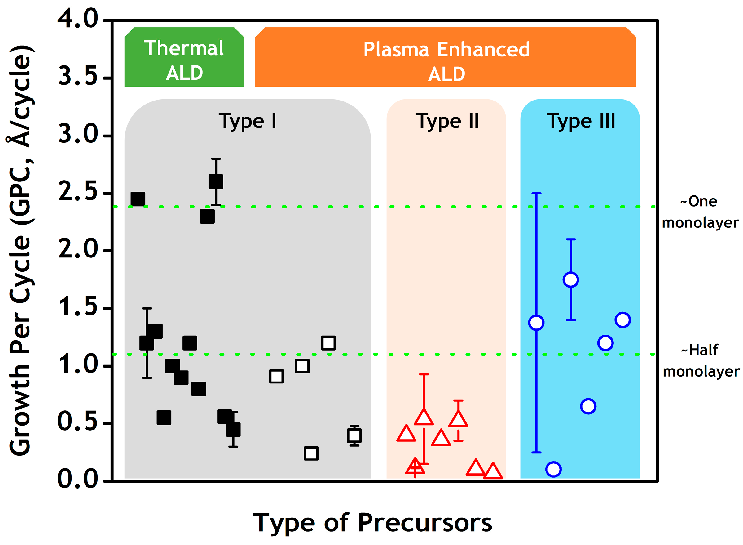
| Type | Classification | Examples | Major Potential Impurities | Deposition Method |
|---|---|---|---|---|
| I | Chlorine-containing precursors | Chlorosilanes: SiH2Cl2, Si2Cl6, etc. | Cl, H, O | PEALD, Thermal ALD |
| II | Carbon-containing precursors | Alkyl-aminosilanes: 3DMAS (SiH(N(CH3)2)3), BTBAS (SiH2(NHtBu)2), etc. | C, H, O | PEALD |
| III | Chlorine-free and carbon-free precursors | SiH4, TSA (N(SiH3)3), NPS ((SiH3)4Si), etc. | H, O | PEALD |
| ALD | Precursor | Reactant | Dosing Pressure (Torr) | Dosage (L) | Deposition Temp. (°C) | GPC (Å/Cycle) | References |
|---|---|---|---|---|---|---|---|
| Thermal | SiCl4 | NH3 | 10 | ~1 × 10¹⁰ | 427–627 | 2.45 | [19] |
| Thermal | SiCl4 | NH3 | 170 | ~5 × 10¹⁰ | 375, 550 | ~0.8 | [24] |
| Thermal | SiH2Cl2 | NH3 | – | ~6 × 10⁹ | 450 | 0.8 | [31] |
| Thermal | Si2Cl6 | NH3 | 1 | ~1 × 10⁷ | 525–650 | 2.3 | [17] |
| Thermal | Si2Cl6 | N2H4 | 1 | ~2 × 10⁸ | 515–557 | 2.4–2.8 | [32] |
| Thermal | SiH2Cl2 | NH3 (HF) | 0.06 | ~5.4 × 10⁶ | 375 | ~1 | [29] |
| Plasma | SiH2Cl2 | NH3 | 0.06 | ~5.4 × 10⁶ | 250–400 | ~0.9 | [16,44] |
| Plasma | Si2Cl6 | NH3 | ~0.07 | ~8 × 10⁵ | 350–450 | 1.2 | [49] |
| Plasma | (SiH3)3N | NH3 | 0.3 | ~6 × 10⁴ | 150–350 | 0.65 | [2,63,64] |
© 2016 by the authors; licensee MDPI, Basel, Switzerland. This article is an open access article distributed under the terms and conditions of the Creative Commons Attribution (CC-BY) license (http://creativecommons.org/licenses/by/4.0/).
Share and Cite
Meng, X.; Byun, Y.-C.; Kim, H.S.; Lee, J.S.; Lucero, A.T.; Cheng, L.; Kim, J. Atomic Layer Deposition of Silicon Nitride Thin Films: A Review of Recent Progress, Challenges, and Outlooks. Materials 2016, 9, 1007. https://doi.org/10.3390/ma9121007
Meng X, Byun Y-C, Kim HS, Lee JS, Lucero AT, Cheng L, Kim J. Atomic Layer Deposition of Silicon Nitride Thin Films: A Review of Recent Progress, Challenges, and Outlooks. Materials. 2016; 9(12):1007. https://doi.org/10.3390/ma9121007
Chicago/Turabian StyleMeng, Xin, Young-Chul Byun, Harrison S. Kim, Joy S. Lee, Antonio T. Lucero, Lanxia Cheng, and Jiyoung Kim. 2016. "Atomic Layer Deposition of Silicon Nitride Thin Films: A Review of Recent Progress, Challenges, and Outlooks" Materials 9, no. 12: 1007. https://doi.org/10.3390/ma9121007