A One-Dimensional Effective Model for Nanotransistors in Landauer–Büttiker Formalism

Department of Computational Physics, Brandenburg University of Technology Cottbus-Senftenberg, PO box 101344, 03013 Cottbus, Germany
Micromachines 2020, 11(4), 359; https://doi.org/10.3390/mi11040359
Submission received: 11 March 2020
/
Accepted: 27 March 2020
/
Published: 30 March 2020
(This article belongs to the Special Issue Miniaturized Transistors, Volume II)
Abstract
:In a series of publications, we developed a compact model for nanotransistors in which quantum transport in a variety of industrial nano-FETs was described quantitatively. The compact nanotransistor model allows for the extraction of important device parameters as the effective height of the source-drain barrier, device heating, and the quality of the coupling between conduction channel and the contacts. Starting from a basic description of quantum transport in a multi-terminal device in Landauer–Büttiker formalism, we give a detailed derivation of all relevant formulas necessary to construct our compact nanotransistor model. Here we make extensive use of the the R-matrix method.
1. Introduction
Around 2005–2010, the transistors obeying Moore’s law where strained high-k metal gate MOSFETs with channel lengths between 20–40 nm. At this point a further reduction of the transistor size in a conventional MOSFET becomes difficult because of short channel effects that reduce the gate voltage control over the conduction channel. To counteract this loss of control new transistor architectures were developed. In industrial applications the FinFET and the SOI transistor architecture hwere applied to continue Moore’s law to presently below 10nm gate length. It is now generally accepted that in this length-regime quantum transport becomes dominant and Moore’s law thus enters the domain of quantum electronics.
In a series of papers [1,2,3,4,5,6,7,8], we developed a compact transistor model in which quantum transport in a variety of industrial nano-FETs could be described quantitatively [6,7,8]. Our compact transistor model allows for the extraction of important device parameters as the effective height of the source-drain barrier of the transistor, device heating, and the overlap between the wave functions in the contacts and in the electron channel thus describing the quality of the coupling between conduction channel and contacts. Our starting point is a general description of quantum transport in a multi-terminal device in Landauer–Büttiker formalism which we formulate in the R-matrix formalism [1,2]. Using the R-matrix formalism as the essential tool, we give in this paper a systematic and comprehensive derivation of all relevant formulas necessary to construct our compact transistor model.
The concept of Landauer–Büttiker formalism was pioneered by Frenkel [9], Ehrenberg and Hönl [10], Landauer [11,12], Tsu and Esaki [13], Fisher and Lee [14], and Büttiker [15,16,17]. The central quantities of Landauer–Büttiker formalism are the transmission coefficients of the scattering solutions of the Schrödinger equation. In recent decades, Landauer–Büttiker formalism has been applied in fundamental research to numerous mesoscopic systems. Well-known examples include interferometric measurements in an Aharonov-Bohm ring [15,18], the quenching of the quantum Hall effect in small junctions [19,20], the quantized conductance in ballistic point contacts [21,22], resonant transport through double barrier systems [23], Coulomb blockade oscillations [24,25], spintronic effects [26,27,28], and Hanbury Brown and Twiss experiments on current fluctuations [29,30,31,32].
For formal developments as well as for numerical- and analytical evaluations of the mentioned transmission coefficients of the scattering functions we employ the R-matrix method. This method was introduced by Wigner and Eisenbud and has been widely used in atomic and nuclear physics (for reviews see Refs. [33,34]). A similar method was developed by Kapur and Peierls [35]. The application of the R-matrix technique to mesoscopic semiconductor systems was demonstrated by Smrčka [36] for one-dimensional structures. Since then it has been applied to a variety of other semiconductor nano-structures as point contacts [37], quantum dots [38,39], resonant tunneling in double barrier systems [40], four-terminal cross-junctions [41], gate all around and double gate MOSFETs [42,43], nanowire transistors [44], spin FETs [45], magneto-transport in nanowires [46], ballistic transport in wrinkled superlattices [47], and spin controlled logic gates [48]. A conceptual advantage of the R-matrix method is that for the construction of the transmission coefficients only properties of general wave function solutions of the time-independent Schrödinger equation are necessary (see Equation (21)). This is in contrast to the often used non-equillibrium Green’s function approach [49] which relies on the calculation of Green’s functions from which the transmission coefficients have to be calculated via the Fisher-Lee relation [14]. Moreover, the existence of the discrete representation of the R-matrix in the eigenbasis of the Wigner–Eisenbud functions (see Equation (22)) allows for the systematic construction of the one-dimensional effective transistor model used in Refs. [6,7,8] as will be described in Section 5, Section 6, Section 7 and Section 8.
2. Landauer–Büttiker Formula for Multi-Terminal Devices
Our model for a multi-terminal system was described in Refs. [1,2]. It consists of a central quantum system located in the scattering volume which is in contact with N terminals denoted with the index (see Figure 1). In the scattering volume the potential acting on charge carriers can be arbitrary. For each terminal we assume the existence of, first, a reservoir for the charge carriers in which their chemical potential is defined and, second, a contact region to the scattering volume in which coherent scattering states are formed (see Equation (4)). The are thus outgoing from this contact and they are coherent in the volume . As illustrated in Figure 1 we define in each a local coordinate system spanned by a triple or orthonormal basis vectors , , and so that we can write
where points to the origin of the local coordinate system. The coordinate varies in the longitudinal direction and and in the two transverse directions. For the interface between and one has with growing towards the interior of the contact region. Furthermore, is the surface normal vector to . We require that the potential energy V of the charge carriers (electrons) in the contact regions takes the form
Here we assume that the reservoir is grounded with the chemical potential . To each of the other reservoirs a gate voltage is applied where we formally define . Then one has . As usual in the Landauer–Büttiker approach, the scattering states which are formed in are occupied according to the Fermi–Dirac distribution function with the chemical potential . Furthermore, in the outgoing parts of the scattering states arriving in s are absorbed completely, without any back-reflection.
Following further the theoretical framework of Landauer and Büttiker we start from the scattering solutions of the stationary Schrödinger equation
in the coherence region . The relevant wave functions can be taken to vanish outside the coherence volume leading to the boundary condition where is the surface of excluding the (see Figure 1). The scattering solutions out-going from contact s can be written in each of the contacts as
Here the transverse mode functions are the solutions of the eigenvalue problem
defining the index of the transverse mode n, the composite mode index , and . The wave numbers of the harmonic waves in Equation (4) are given by
The first factor on the right hand side of Equation (4) is the in-going part characterizing the scattering state. The second factor on the r.h.s. contains the out-going components which are determined by the S-matrix . In Section 3 we construct the S-matrix in the R-matrix approach.
The total electric current in terminal s is calculated in Appendix A. We find
with the Fermi–Dirac distribution , the elementary charge e, the current transmission sum
and the current S-matrix
3. Construction of the S-matrix with the R-matrix Method
We write the general solution of Equation (3) in each of the in the form
Because of the linearity of the problem the S-matrix in Equation (4) can be defined as the linear mapping from the onto the of the form
To construct we expand the wave function in the scattering volume in the orthonormal and complete set of Wigner–Eisenbud functions ,
with
(see Appendix B). The Wigner–Eisenbud functions are the solutions of the Schrödinger equation
in the domain . Here one imposes Wigner–Eisenbud boundary conditions, i.e., Neumann boundary conditions of vanishing normal derivative on the ,
and Dirichlet boundary conditions on the remaining surface of denoted with writing
In Appendix B, we show that Wigner–Eisenbud energies are real and that the Wigner–Eisenbud functions can be chosen real. The normalization is taken as . To calculate the expansion coefficients we multiply Equation (3) from the left with and Equation (14) from the left with . Subtraction of the former equation from the latter and subsequent integration over the whole domain yields with the second Green’s identity
In the area integration of Equation (17) as well as in the remaining area integrations over the we assume according to Equation (1) the parameterization of so that
Using in Equation (17) the notation
for the outward surface derivative, applying Equation (13) on the l. h. s., and inserting the boundary conditions for the Wigner–Eisenbud functions, one obtains
For we write and establish the expansion
in the complete orthonormal and real function system of the with
An analogous expansion
holds for the surface derivative. Inserting the expansions Equations (23) and (25) in Equation (21) one obtains after a projection onto
with the R-matrix
where
Inserting in Equation (26) and one arrives at
Defining further a diagonal k-matrix we formally write
Here we exploited that for three square matrices one has . The current transmission matrix is thus seen to be symmetrical while the S-matrix is not symmetrical.
4. Transistor Model
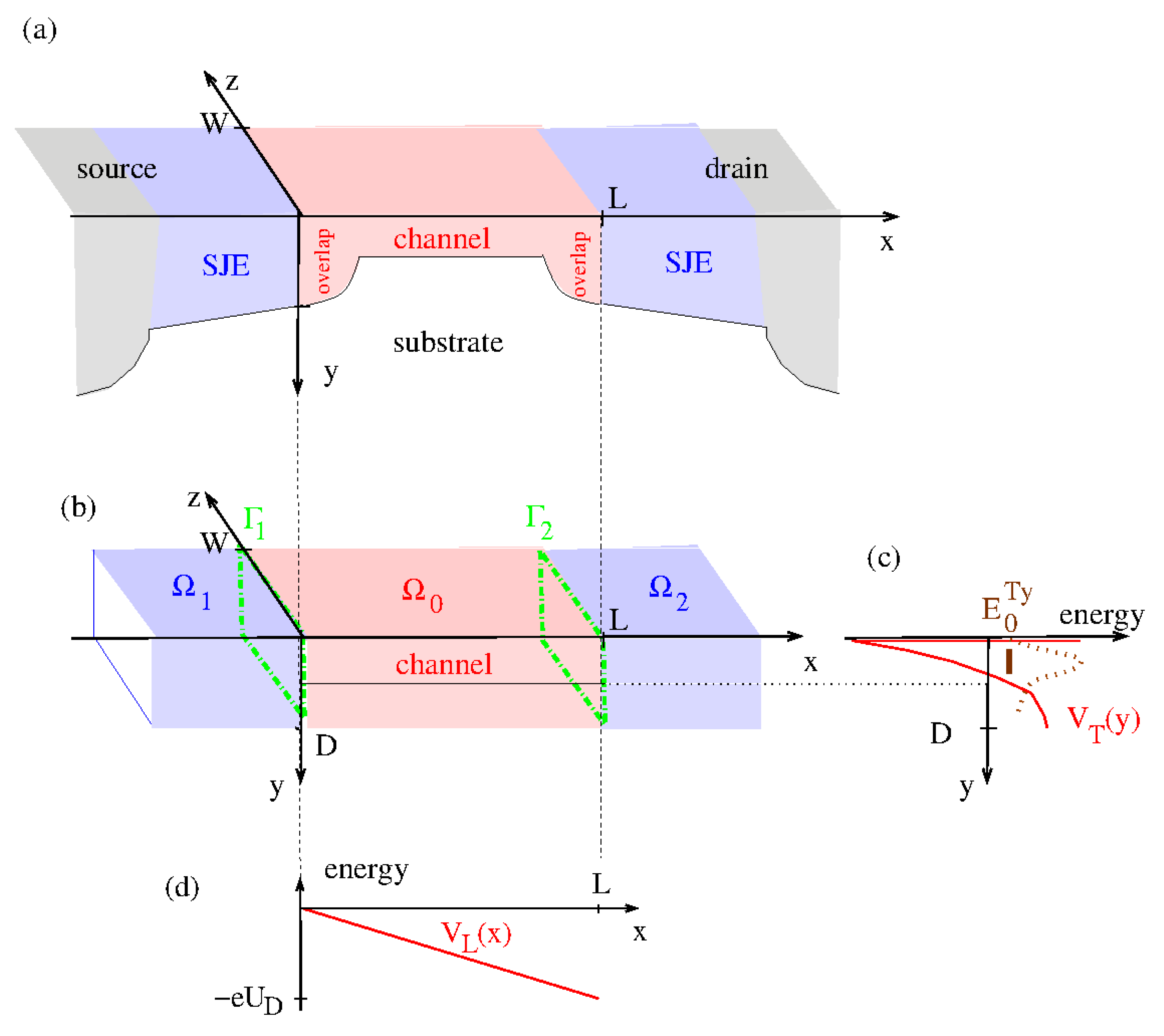
The application of our model for a general multi-terminal system in Section 2 to a conventional n-channel nano-MOSFET is discussed in Ref. [1] (see in particular Figure 3 therein) and in Ref. [2]. Neglecting tunneling currents to the gate we here treat the transistor as a two-terminal device including only the source, , and the drain, . The relevant structure elements of a nano-MOSFET can be taken from Figure 2a depicting the heavily n-doped source- and drain contact, the shallow junction extensions (SJEs) of the contacts, the conduction channel in the p-substrate, and the overlap of the conduction channel with the SJE. The semiconductor-insulator interface is located at . It is represented by a cut-off of the wave functions. The assignment of the structure elements of the nano-MOSFET to the structure elements of the general multi-terminal system in Figure 1 is shown in Figure 2b: The SJEs are assumed to be identical to having the depth D. The SJE of the source is then associated with the cubic contact region with , , and . Here W is the width of the transistor. The SJE of the drain is associated with the cubic contact region with , , and . Here and are semi-infinite corresponding to (see Figure A1). The cubic scattering region with , , and includes the conduction channel of length L and the overlap of the conduction channel with the SJEs. The interfaces are located at for and at for . The basis vectors of the local coordinate systems in Equation (1) are and for the outward normal vectors. Furthermore, we choose and . The local coordinates are , , , and . In Equation (2) we assume the simplest case renaming for . We take the limit as well as so that electron gas in the heavily doped source and drain in and can be treated as a three dimensional free Fermi gas with the chemical potential
where is the inverse function the Fermi–Dirac integral
The Fermi energy above the bottom of the conduction band is given by
with the doping concentration in the contacts (full ionization of donors), the valley-degeneracy and the effective mass taken as . Here and are the effective masses corresponding to the principle axes of the constant energy ellipsoids.
For the potential in the scattering area we choose a separable form
(see Figure 2c,d). Here the transverse potential is the confinement potential for the conduction channel of the transistor. A natural choice for is the confinement potential present in a simple MOS-structure without source- and drain contact as discussed in Refs. [50,51]. Then corresponds to the potential determined in Equation (4) of [50]. As pointed out in Refs. [50,51] in the electron channel a strong lateral sub-band quantization exists so that only the lowest subband of the channel confinement potential with a bottom energy of corresponding to in Ref. [50] is occupied (see Figure 2c and Equation (62)). Here only the two constant energy ellipsoids with the heavy mass perpendicular to the (100)-interface are occupied. This leads to a valley degeneracy of in the channel and the effective mass entering (3) is the light mass [5]. The longitudinal potential arises from the applied drain voltage assumed to fall off linearly so that
The described transistor model has several special properties which can be used to simplify our general multi-terminal model described in Section 2:
- P1
- The transistor is treated as two-terminal system.
- P2
- Axial contacts: For all the surface normal vectors are aligned so that . For our transistor model .
- P3
- Global separability (see Figure 2b): In a system with axial contacts in -direction the potential in the scattering area is the sum of a longitudinal potential varying in -direction and transverse potential varying in the two transverse directions. In the transistor model this separation is given in Equation (35).
- P4
- P5
- Planarity: For a planar device one can define one or two global transverse coordinates valid in all and in on which the potential does not depend. In our transistor model one global transverse coordinate exists which is the width-coordinate z.
- P7
- Single mode approximation: One assumes strong transverse quantization in the scattering area. Then splitting of the transverse quantum levels induced by is so strong that only the lowest transverse level has to be taken into account.
As we will demonstrate in the next sections, on account of the listed special properties the R-matrix approach allows for a systematic reduction of the general theory for a multi-terminal device to a one-dimensional effective transistor model.
5. The R-matrix in a Separable Two-Terminal System
We consider a two-terminal system as in Figure 2b which fulfills the global separability condition P3 in Section 4 (see Figure 3). Inserting the separable potential Equation (35) in Equation (14) makes possible a product ansatz for the Wigner–Eisenbud functions
with . Here the transverse functions are defined by
with the boundary conditions
The longitudinal functions are the solutions of
with the one-dimensional Wigner–Eisenbud boundary conditions
The product ansatz Equation (37) is permissible in the two-terminal system since the one-dimensional Wigner–Eisenbud boundary condition in Equation (41) is compatible with the general Wigner–Eisenbud boundary conditions in Equations (15) and (16). To construct the R-matrix with Equation (37) we write Equation (28) as
the overlap factor
The Equation (27) becomes
6. Effective Approximation and One-Dimensional Effective Scattering Problems
In effective approximation Equation (6) is simplified in the form
where is the smallest transverse mode energy, . One then finds from Equations (30) and (45)
with
The inversion of in Equation (31) can now be carried out analytically with the result
With this relation Equation (A4) becomes with
with the overlap matrix
In Appendix D, we demonstrate that instead of using Equation (48) to find with subsequent inversion one can calculate the matrices occurring in Equation (51) according to
Here the are the transmission coefficients resulting in an effective one-dimensional scattering problem associated with the 1d-Schrödinger equation
with effective scattering potential
Here the asymptotics of the source incident scattering states of the effective scattering problem associated with Equation (54) are given by
and
Appendix E contains a simple, stable and fast recursive algorithm which we used to find the effective transmission coefficients . It is seen from Equation (55) that the quantum levels of the confinement potential in the conduction channel that arise in Equation (38) act as offsets in the effective potential.
7. Planar Systems and Supply Functions
In planar systems, the potential is taken as translationally invariant in the z-direction so that and . For the interface regions we insert in Equation (5)
to find
with and
Furthermore from Equation (48) one has
with the conserved energy in the -plane
and from Equation (46) , where . In Appendix F it is derived that
with wave function overlap
and the supply function
In the limit we can write with
Upon introducing
it results that
Here the Fermi–Dirac-Integral is given by
with .
In Appendix D, we show that one can calculate the matrices in Equation (67) from the transmission coefficients resulting in a modified effective one-dimensional scattering problem. Here Equations (53)–(57) are substituted by
for
and
8. Single-Mode Approximation and One-Dimensional Effective Model
As pointed out in Section 4, for a conventional nanotransistor only the lowest subband of the channel confinement potential with a bottom energy of resulting at is occupied (see Figure 2c and Equation (62)). Taking into account only -terms Equation (67) becomes
with
(compare with Equation (1) of Ref. [8]). Here we neglected in the wave function overlap the energy dependence, and introduced the valley degeneracy of in the n-type conduction channel.
As described in Section 7 the effective transmission coefficient is calculated from the source-incident scattering states of the 1d-Schrödinger Equation (74) with the effective scattering potential given by
where set in Equation (75) (linear decrease of the drain voltage) and . The parameter is interpretable as the effective height of the source-drain barrier. The parameters and C as well as T are adjusted to experiments in Refs. [6,7,8].
9. Summary
Starting from a basic description of quantum transport in a multi-terminal device in Landauer–Büttiker formalism in Refs. [1,2] we give a detailed derivation of all relevant formulas necessary to construct a one-dimensional effective model for a nanotransistor described in Refs. [6,7,8]. In this model, quantum transport in nano-FETs can be described quantitatively. Important device parameters can be extracted as the effective height of the source-drain barrier of the transistor, device heating, and the quality of the coupling between conduction channel and contacts.
Funding
This research received no external funding.
Conflicts of Interest
The author declares no conflict of interest.
Appendix A. Derivation of the Formula for the Current
We calculate the total current in contact s starting from the decomposition
(see Figure A1). Here is the absolute value of the current in contact s created by the in-going parts of all scattering states
where . Furthermore, is the absolute value of the current in contact s created by the out-going parts of all scattering states where , and are arbitrary, thus including the case also. From current conservation one has
In Figure A1 the direction of the current contributions is given by the arrows for positive charge carriers. For n-type conduction the arrows have to be reversed.
Figure A1.
The formulation of Equation (A1) for contact in a -terminal device at (see also Figure 1). The current component directed in -direction is . The three current components in -direction are , , and . Because there are no scattering processes in it holds that and are the same in and (see dashed horizontal lines).

Appendix A.1. Current Contribution of a Single Scattering State
We decompose
where is the absolute value of the current in contact created by the out-going part of the scattering state given by
Here for
with
since from Equation (A4) the case can be excluded. In Equation (A8) is the continuum normalization constant to be constructed in Equation (A17). The issue of the k-summation in Equation (A5) is addressed in Appendix A.2. From Equation (4) we have for
and
where
The area integration in Equation (A6) leads to
where the index restricts the summation to propagating waves with real, positive .
Appendix A.2. Summation Over Scattering States
To calculate according to Equation (A5) one sums Equation (A12) over all scattering states, i. e. over all n and k, according to their occupation in the form
with the discretization
Here the constant is the density of scattering states in k-space which we will address in Equation (A16). The width of the k-intervals is assumed to be small so that the k-integration can be replaced by a Riemann sum. As usual, one determines and by assigning to each normalized propagating solution of the Schrödinger equation in of the form
the normalized scattering state which has the in-going part in Equation (A15). As is well-known, this corresponds to the expectation that each in-coming particle is represented by a wave-package. When the particle is located deeply in the interior of it does not ’feel’ the quantum system and it can be equivalently represented by a superposition of the plane waves in Equation (A15) or the in-going part of the normalized scattering states . The plane waves solutions Equation (A15) can now be counted and normalized introducing artificial boundary conditions in in the interval (see Figure A1) so that
where in the last step we included a simple spin-degeneracy factor of two. The normalization then follows from
Upon insertion in Equation (A13) one finds with
Substituting further
so that
Appendix B. Properties of the Wigner–Eisenbud Problem
- (1)
- Hermiticity:We take two functions and obeying the Wigner–Eisenbud boundary conditions Equations (15) and (16), i. e., with the Neumann boundary conditions and Dirichlet boundary condition . From second Green’s theorem it follows directly thatAs desired, one immediately obtains the hermicity condition
- (2)
- The Wigner–Eisenbud energies are real:The Wigner–Eisenbud functions are the eigenfunctions of H,obeying Wigner–Eisenbud conditions. Setting in Equation (A25) it follows that
- (3)
- The Wigner–Eisenbud functions can be chosen real:Since the are real the complex conjugate of Equation (A26) is given byTherefore, if a complex function is a solution of Equation (A26) then is a solution too and one can choose instead of two real solutions and .
- (4)
- The Wigner–Eisenbud functions are orthogonal:For two Wigner–Eisenbud functions with different energies we writeSetting in Equation (A25) andFor degenerate Wigner–Eisenbud functions two orthogonal linear combinations can be constructed with standard methods.
- (5)
- Completeness:As described in (1) the operator H is hermitic, it is second order in the derivatives and linear. Then the set of its eigenfunctions , the Wigner–Eisenbud functions, is complete. Thus, with (3) and (4) the can be chosen as a complete, real, orthonormal function system.
Appendix C. Verification of Equation (49)
We verify this equation explicitly:
Here we applied the relations in under-braces
To derive the first relation we formulate the completeness of the and the writing
Projection onto and yields immediately
The second relation in Equation (A34) is derived by inserting in the orthogonality relation
the expansion . It is seen that
Appendix D. R-matrix Theory in One Dimension
We define the Wigner–Eisenbud functions in one dimension as the solutions of the hermitic eigenvalue problem
with the effective 1d-scattering potential given in Equation (55) and von-Neumann boundary conditions
A comparison with Equation (40) yields identical eigenfunctions and eigenenergies shifted by ,
The constitute a complete orthonormal system in which the scattering states in Equation (54) can be expanded in the domain . One has
where
The left-multiplication of Equation (54) with and left-multiplication of Equation (A39) with leads after integration to
Partial integration on the left side and application of the von-Neumann boundary conditions Equation (A40) leads to
Upon multiplication with and summation one finds
with
From evaluation of this equation for and one finds in correspondence to Equation (26)
where we define the R-matrix
and the two-component vectors
We now proceed as in Equation (10) and decompose the general solution of the wave function in the contacts in an in-going part and an out-going part, , where
and
As in Equation (11), the S-matrix is the linear mapping of the in-going part onto the out-going part
with the two-component vector
The source-incident scattering states are associated with and , and . The drain-incident scattering states are associated with and , and . One finds the relation between S-matrix and the transmission- and reflection coefficients
It follows that
with the diagonal wave number matrix . From Equation (A49), , and Equation (A60) it follows that
A comparison with Equation (A55) leads to
For the current matrix we find with Equation (A52)
It is now decisive that with the definition of the in Equation (A50) it results that
identical with Equation (48). From Equation (A57) one has
In Section 6, we identified with the source-incident scattering state characterized through the asymptotic in Equations (76) and (77). Therefore we identify and Equation (A70) becomes Equation (53).
In Equation (65) we define for the planar system in Section 7
with the conserved energy in the -plane
and . Comparing Equation (A66) with Equation (A64) one can adopt the result Equation (A70) for the planar system if one identifies , , and . This way an effective one-dimensional scattering problem associated with the 1d-Schrödinger equation
results with the effective scattering potential in the limit given by
The transmission coefficients of the source-incident scattering functions of Equation (A68) yield
Appendix E. Numerical Evaluation of the Transmission Coefficients in One Dimension
In the finite difference method, the one-dimensional Schrödinger equation
becomes
Here we discretize the real axis in the form with . Requiring one has grid points in the scattering area . Furthermore, we introduce , , and . In view of Equation (81) we assume the asymptotics (source) and (drain). The source-incident scattering states then follow the asymptotic
with with and . To construct the source-incident scattering states we transform Equation (A72) for into a downward recursion
For one has
with the known asymptotic on the drain side
The the downward recursion Equation (A74) is started with, for example,
to construct in the entire range. Especially one obtains
and
Appendix F. Derivation of the Supply Function
References
- Nemnes, G.A.; Wulf, U.; Racec, P.N. Nano-transistors in the Landauer-Büttiker formalism. J. Appl. Phys. 2004, 96, 596. [Google Scholar] [CrossRef]
- Nemnes, G.A.; Wulf, U.; Racec, P.N. Nonlinear I-V characteristics of nanotransistors in the Landauer-Büttiker formalism. J. Appl. Phys. 2005, 98, 84308. [Google Scholar] [CrossRef]
- Wulf, U.; Richter, H. Scale-invariant drain current in nano-FETs. J. Nano Res. 2010, 10, 49–61. [Google Scholar] [CrossRef] [Green Version]
- Wulf, U.; Richter, H. Scaling in quantum transport in silicon nano-transistors. Solid State Phenom. 2010, 10, 156–158. [Google Scholar] [CrossRef] [Green Version]
- Wulf, U.; Richter, H. Scaling properties of ballistic nano-transistors. Nanoscale Res. Lett. 2011, 6, 365. [Google Scholar] [CrossRef] [Green Version]
- Wulf, U.; Krahlisch, M.; Kučera, J.; Richter, H.; Höntschel, J. A quantitative model for quantum transport in nano-transistors. Nanosyst. Phys. Chem. Math. 2013, 4, 800–809. [Google Scholar]
- Wulf, U.; Kučera, J.; Richter, H.; Wiatr, M.; Höntschel, J. Characterization of nanotransistors in a semiempirical model. Thin Solid Films 2016, 613, 6–10. [Google Scholar] [CrossRef]
- Wulf, U.; Kučera, J.; Richter, H.; Horstmann, M.; Wiatr, M.; Höntschel, J. Channel Engineering for Nanotransistors in a Semiempirical Quantum Transport Model. Mathematics 2017, 5, 68. [Google Scholar] [CrossRef] [Green Version]
- Frenkel, J. On the electrical resistance of contacts between solid conductors. Phys. Rev. 1930, 36, 1604. [Google Scholar] [CrossRef]
- Ehrenberg, W.; Hönl, H. Zur Theorie des elektrischen Kontakte. Zeitschrift für Phys. 1931, 68, 289. [Google Scholar] [CrossRef]
- Landauer, R. Spatial variation of currents and fields due to localized scatterers in metallic conduction. IBM J. Res. Develop. 1957, 1, 223. [Google Scholar] [CrossRef]
- Landauer, R. Electrical transport in open and closed systems. Z. Phys. B 1987, 68, 217. [Google Scholar] [CrossRef]
- Tsu, R.; Esaki, L. Tunneling in a finite superlattice. Appl. Phys. Lett. 1973, 22, 562. [Google Scholar] [CrossRef]
- Fisher, D.S.; Lee, P.A. Relation between conductivity and transmission matrix. Phys. Rev. B 1981, 23, 6851. [Google Scholar] [CrossRef] [Green Version]
- Büttiker, M.; Imry, Y.; Landauer, R.; Pinhas, S. Generalized many-channel conductance formula with application to small rings. Phys. Rev. B 1985, 31, 6207. [Google Scholar] [CrossRef] [Green Version]
- Büttiker, M. Four-terminal phase-coherent conductance. Phys. Rev. Lett. 1986, 57, 1761. [Google Scholar] [CrossRef]
- Büttiker, M. Symmetry of electrical conduction. IBM J. Res. Dev. 1988, 32, 317. [Google Scholar] [CrossRef]
- Sharvin, D.Y.; Sharvin, Y.V. Magnetic-flux quantization in a cylindrical film of a normal metal. JETP Lett. 1981, 34, 272. [Google Scholar]
- Roukes, M.L. Quenching of the Hall effect in a one-dimensional wire. Phys. Rev. Lett. 1987, 59, 3011. [Google Scholar] [CrossRef] [Green Version]
- Baranger, H.U.; Stone, A.D. Quenching of the Hall resistance in ballistic microstructures: A collimation effect. Phys. Rev. Lett. 1989, 63, 414. [Google Scholar] [CrossRef]
- van Wees, B.J.; van Houten, H.; Beenakker, C.W.J.; Williamson, J.G.; Kouwenhoven, L.P.; van der Marel, D.; Foxon, C.T. Quantized conductance of point contacts in a two-dimensional electron gas. Phys. Rev. Lett. 1988, 60, 848. [Google Scholar] [CrossRef] [Green Version]
- Wharam, D.A.; Thornton, T.H.; Newbury, R.; Pepper, M.; Ahmed, H.; Frost, J.E.F.; Hasko, D.G.; Peacock, D.C.; Ritchie, D.A.; Jones, G.A.C. One-dimensional transport and the quantisation of the ballistic resistance. J. Phys. C 1988, 21, L209. [Google Scholar] [CrossRef]
- Mizuta, H.; Tanoue, T. The Physics and Applications of Resonant Tunneling Diodes. In Cambridge Studies in Semiconductor Physics and Microelectronic Engineering 2; Cambridge University Press: Cambridge, UK, 1995. [Google Scholar]
- Meirav, U.; Kastner, M.A.; Wind, S.J. Single-electron charging and periodic conductance resonances in GaAs nanostructures. Phys. Rev. Lett. 1990, 65, 771. [Google Scholar] [CrossRef] [PubMed]
- Meir, Y.; Wingreen, N.S.; Lee, P.A. Transport through a strongly interacting electron system: Theory of periodic conductance oscillations. Phys. Rev. Lett. 1991, 66, 3048. [Google Scholar] [CrossRef] [PubMed]
- Awschalom, D.D.; Loss, D.; Samarth, N. (Eds.) Semiconductor Spintronics and Quantum Computation; Springer: Berlin, Germany, 2002. [Google Scholar]
- Greilich, A.; Yakovlev, D.R.; Shabev, A.; Efros, A.L.; Yugova, I.A.; Oulton, R.; Stavarche, V.; Reuter, D.; Wieck, A.; Bayer, M. Mode locking of electron spin coherences in singly charged quantum dots. Science 2006, 313, 341. [Google Scholar] [CrossRef] [PubMed] [Green Version]
- Koppens, F.H.L.; Buizert, C.; Tielrooij, K.J.; Nowack, K.C.; Meunier, T.; Kouwenhoven, L.P.; Vandersypen, L.M.K. Driven coherent oscillations of a single electron spin in a quantum dot. Nature 2006, 442, 766. [Google Scholar] [CrossRef]
- Brown, R.H.; Twiss, R.Q. A new type of interferometer for use in radio astronomy. Philos. Mag. 1954, 45, 663–682. [Google Scholar] [CrossRef]
- Büttiker, M. Scattering theory of current and intensity noise correlations in conductors and wave guides. Phys. Rev. B 1992, 46, 12485. [Google Scholar] [CrossRef]
- Henny, M.; Oberholzer, S.; Strunk, C.; Heinzel, T.; Ensslin, K.; Holland, M.; Schönenberger, C. The fermionic hanbury brown and twiss experiment. Science 1999, 284, 296. [Google Scholar] [CrossRef] [Green Version]
- Chen, Y.; Webb, R.A. Positive Current Correlations Associated with Super-Poissonian Shot Noise. Phys. Rev. Lett. 2006, 97, 66064. [Google Scholar] [CrossRef]
- Lane, A.M.; Thomas, R.G. R-Matrix Theory of Nuclear Reactions. Rev. Mod. Phys. 1958, 30, 257. [Google Scholar] [CrossRef]
- Burke, P.G.; Berrington, K.A. (Eds.) Atomic and Molecular Processes: An R-matrix Approach; Institute of Physics Publishing: Bristol, UK, 1993. [Google Scholar]
- Kapur, P.L.; Peierls, R. The dispersion formula for nuclear reactions. Proc. Roy. Soc. (London) 1938, A166, 277. [Google Scholar]
- Smrčka, L. R-matrix and the coherent transport in mesoscopic systems. Superlattices Microstruct. 1990, 8, 221. [Google Scholar] [CrossRef]
- Wulf, U.; Kučera, J.; Racec, P.N.; Sigmund, E. Transport through quantum systems in the R-matrix formalism. Phys. Rev. B 1998, 58, 16209. [Google Scholar] [CrossRef]
- Onac, E.; Kučera, J.; Wulf, U. Vertical magnetotransport through a quantum dot in the R-matrix formalism. Phys. Rev. B 2001, 63, 85319. [Google Scholar] [CrossRef]
- Racec, E.R.; Wulf, U.; Racec, P.N. Fano regime of transport through open quantum dots. Phys. Rev. B 2010, 82, 85313. [Google Scholar] [CrossRef] [Green Version]
- Racec, E.R.; Wulf, U. Resonant quantum transport in semiconductor nanostructures. Phys. Rev. B 2001, 64, 115318. [Google Scholar] [CrossRef]
- Jayasekera, T.; Morrison, M.A.; Mullen, K. R-matrix theory for magnetotransport properties in semiconductor devices. Phys. Rev. B 2006, 74, 235308. [Google Scholar] [CrossRef] [Green Version]
- Mil’nikov, G.; Mori, N.; Kamakura, Y.; Ezaki, T. R-matrix theory of quantum transport and recursive propagation method for device simulations. J. Appl. Phys. 2008, 104, 044506. [Google Scholar] [CrossRef]
- Mil’nikov, G.; Mori, N.; Kamakura, Y. R-matrix method for quantum transport simulations in discrete systems. Phys. Rev. B 2009, 79. [Google Scholar] [CrossRef]
- Nemnes, G.A.; Ion, L.; Antohe, S. Self-consistent potentials and linear regime conductance of cylindrical nanowire transistors in the R-matrix formalism. J. Appl. Phys. 2009, 106, 11371. [Google Scholar] [CrossRef]
- Nemnes, G.A.; Manolescu, A.; Gudmundsson, V. Reduction of ballistic spin scattering in a spin-FET using stray electric fields. J. Phys. Conf. Sert 2012, 338, 012012. [Google Scholar] [CrossRef]
- Manolescu, A.; Nemnes, G.A.; Sitek, A.; Rosdahl, T.O.; Erlingsson, S.I.; Gudmundsson, V. Conductance oscillations of core-shell nanowires in transversal magnetic fields. Phys. Rev. B 2016, 93, 205445. [Google Scholar] [CrossRef] [Green Version]
- Mitran, T.; Nemnes, G.; Ion, L.; Dragoman, D. Ballistic electron transport in wrinkled superlattices. Phys. E 2016, 81, 131. [Google Scholar] [CrossRef] [Green Version]
- Nemnes, G.A.; Dragoman, D. Reconfigurable quantum logic gates using Rashba controlled spin polarized currents. Physica E 2019, 111, 13. [Google Scholar] [CrossRef]
- Datta, S. Electronic Transport in Mesoscopic Systems; Cambridge University Press: Cambridge, UK, 1995. [Google Scholar]
- Stern, F. Self-Consistent Results for n-Type Si Inversion Layers. Phys. Rev. B 1972, 5, 4891. [Google Scholar] [CrossRef]
- Ando, T.; Fowler, A.B.; Stern, F. Electronic properties of two-dimensional systems. Rev. Mod. Phys. 1982, 54, 437. [Google Scholar] [CrossRef]
Figure 1.
Idealized multi-terminal system: terminals denoted with the index s are connected to the central scattering volume (red). Each terminal is associated, first, with a charge carrier reservoir defining the chemical potential (grey) of the carriers. Second, it is associated with a contact region (blue) in which coherent scattering states are formed. In green we plot the interfaces between the and (solid) as well as the interfaces between the and (dashed). The coherence volume of the scattering states comprises the set union of and all . Here is the surface of excluding the (magenta).

Figure 2.
(a) Structure elements of a conventional nano-MOSFET: Source- and drain contact with shallow junction extensions SJEs, the latter in blue. In red the conduction channel and the overlap between conduction channel and SJE. The semiconductor-insulator interface is located at . (b) Assignment of the above structure elements to the structure elements of the general multi-terminal system in Figure 1: The SJEs are associated with cubic contact regions . (c) In red: Transverse confinement potential of the conduction channel in the separable ansatz for the potential in Equation (35). In brown the lowest subband energy in the channel confinement potential as defined in Equation (62) (solid) and the corresponding eigenfunction (dotted). (d) Linear drop of the applied drain voltage leading to a linear longitudinal potential in Equation (35).

Figure 3.
The two-terminal system in Figure 2b where the z-direction is omitted for simplicity. Axial contacts in x-direction: points in x-direction, in minus x-direction.
Figure 3.
The two-terminal system in Figure 2b where the z-direction is omitted for simplicity. Axial contacts in x-direction: points in x-direction, in minus x-direction.

© 2020 by the author. Licensee MDPI, Basel, Switzerland. This article is an open access article distributed under the terms and conditions of the Creative Commons Attribution (CC BY) license (http://creativecommons.org/licenses/by/4.0/).
Share and Cite
MDPI and ACS Style
Wulf, U. A One-Dimensional Effective Model for Nanotransistors in Landauer–Büttiker Formalism. Micromachines 2020, 11, 359. https://doi.org/10.3390/mi11040359
AMA Style
Wulf U. A One-Dimensional Effective Model for Nanotransistors in Landauer–Büttiker Formalism. Micromachines. 2020; 11(4):359. https://doi.org/10.3390/mi11040359
Chicago/Turabian StyleWulf, Ulrich. 2020. "A One-Dimensional Effective Model for Nanotransistors in Landauer–Büttiker Formalism" Micromachines 11, no. 4: 359. https://doi.org/10.3390/mi11040359
Note that from the first issue of 2016, this journal uses article numbers instead of page numbers. See further details here.