Article

Suppressing the Initial Growth of Sidewall GaN by Modifying Micron-Sized Patterned Sapphire Substrate with H3PO4-Based Etchant

1
Department of Materials Science and Engineering, National Chaio Tung University, Hsinchu 300, Taiwan
2
Department of Photonics, National Cheng Kung University, Tainan City 701, Taiwan
3
National Nano Device Laboratories, Hsinchu300, Taiwan
*
Author to whom correspondence should be addressed.
Micromachines 2018, 9(12), 622; https://doi.org/10.3390/mi9120622
Submission received: 3 October 2018 / Revised: 22 November 2018 / Accepted: 22 November 2018 / Published: 26 November 2018
(This article belongs to the Special Issue Wide Bandgap Semiconductor Based Micro/Nano Devices)

Abstract

:
Micron-sized patterned sapphire substrates (PSS) are used to improve the performance of GaN-based light-emitting diodes (LEDs). However, the growth of GaN is initiated not only from the bottom c-plane but also from the sidewall of the micron-sized patterns. Therefore, the coalescence of these GaN crystals creates irregular voids. In this study, two kinds of nucleation layers (NL)—ex-situ AlN NL and in-situ GaN NL—were used, and the growth of sidewall GaN was successfully suppressed in both systems by modifying the micron-sized PSS surface.

1. Introduction

High-brightness GaN-based light-emitting diodes (LEDs) are used in a wide variety of applications [1,2]. However, a GaN epitaxial layer usually contains several defects due to the large lattice mismatch and the thermal expansion coefficient difference between GaN and sapphire.
An AlN (or GaN) nucleation layer (NL) is commonly introduced prior to growth of GaN epilayer to overcome this lattice mismatch problem [3,4]. Moreover, micron-sized patterned sapphire substrates (PSS) have been successfully used to reduce these defects and enhance the performance of LEDs [5,6,7,8,9,10,11,12].
When PSS are used, the growth of GaN is initiated not only from the bottom c-plane but also from the sidewall of the micron-sized patterns [13,14,15,16]. As the growth time increases, irregular voids are created during the coalescence of these GaN crystals [17].
A GaN NL is usually deposited by metal–organic chemical vapor deposition (MOCVD), and it is called in-situ GaN NL. An AlN NL can be deposited either by MOCVD or sputtered physical vapor deposition (PVD), and they are generally called in-situ AlN NL and ex-situ AlN NL, respectively. It has been found that ex-situ sputtered AlN NL has better GaN quality than in-situ GaN NL and in-situ AlN NL [15,18].
In this study, sulfuric–phosphoric acid was used to modify the micron-sized patterns in order to suppress the growth of sidewall GaN. The effect of this modification on the growth mechanism of GaN was also investigated.

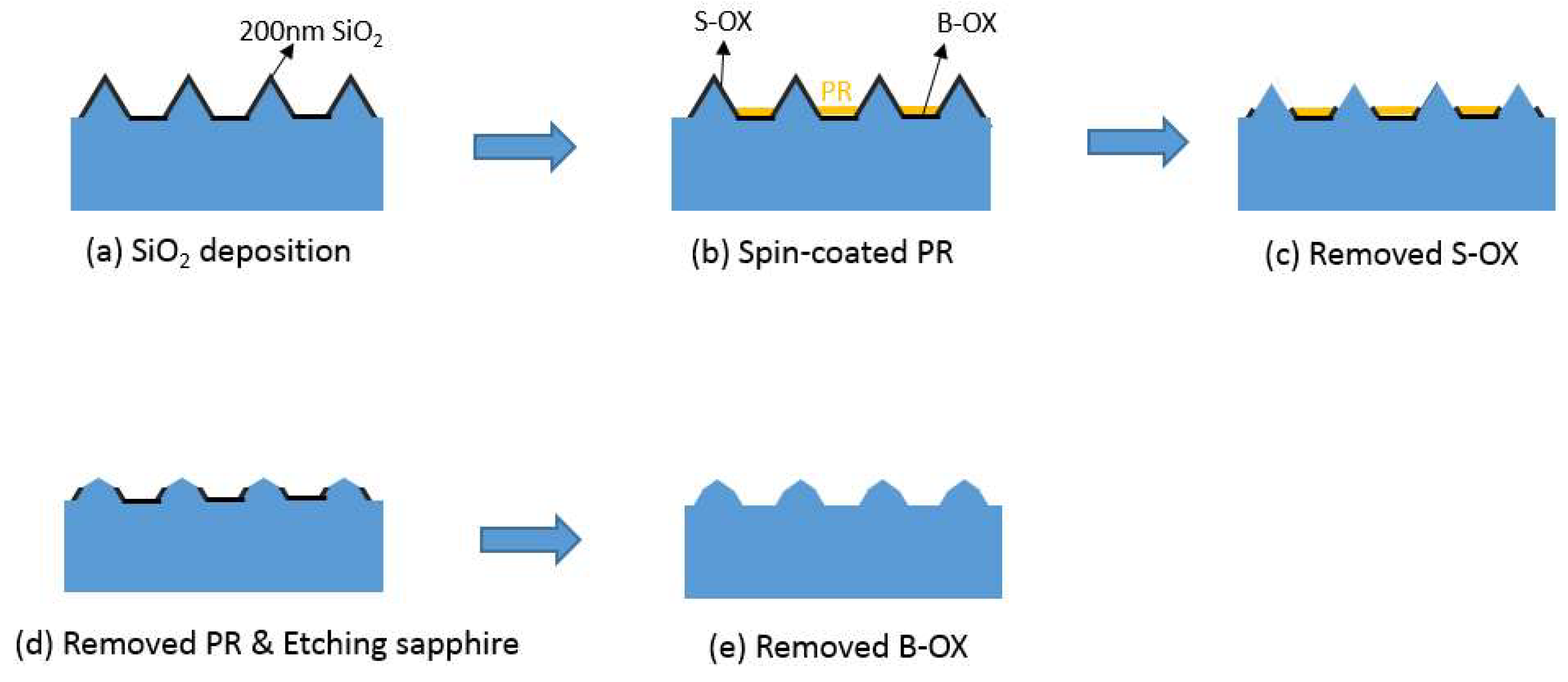
2. Materials and Methods
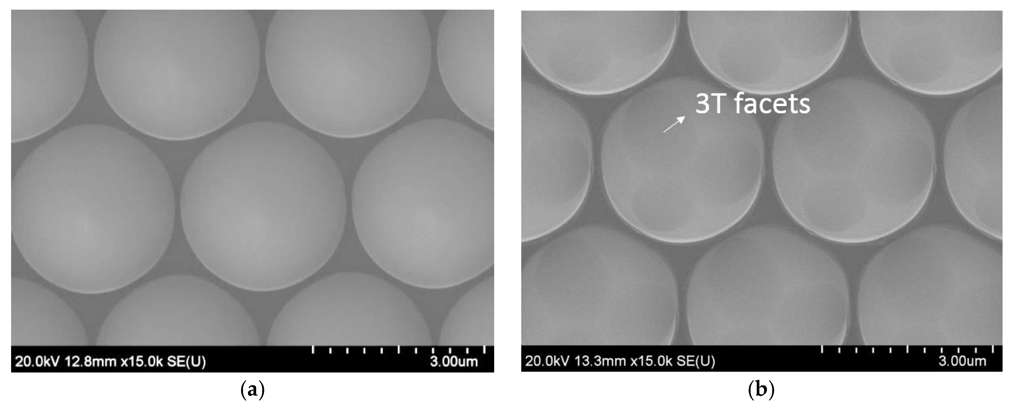
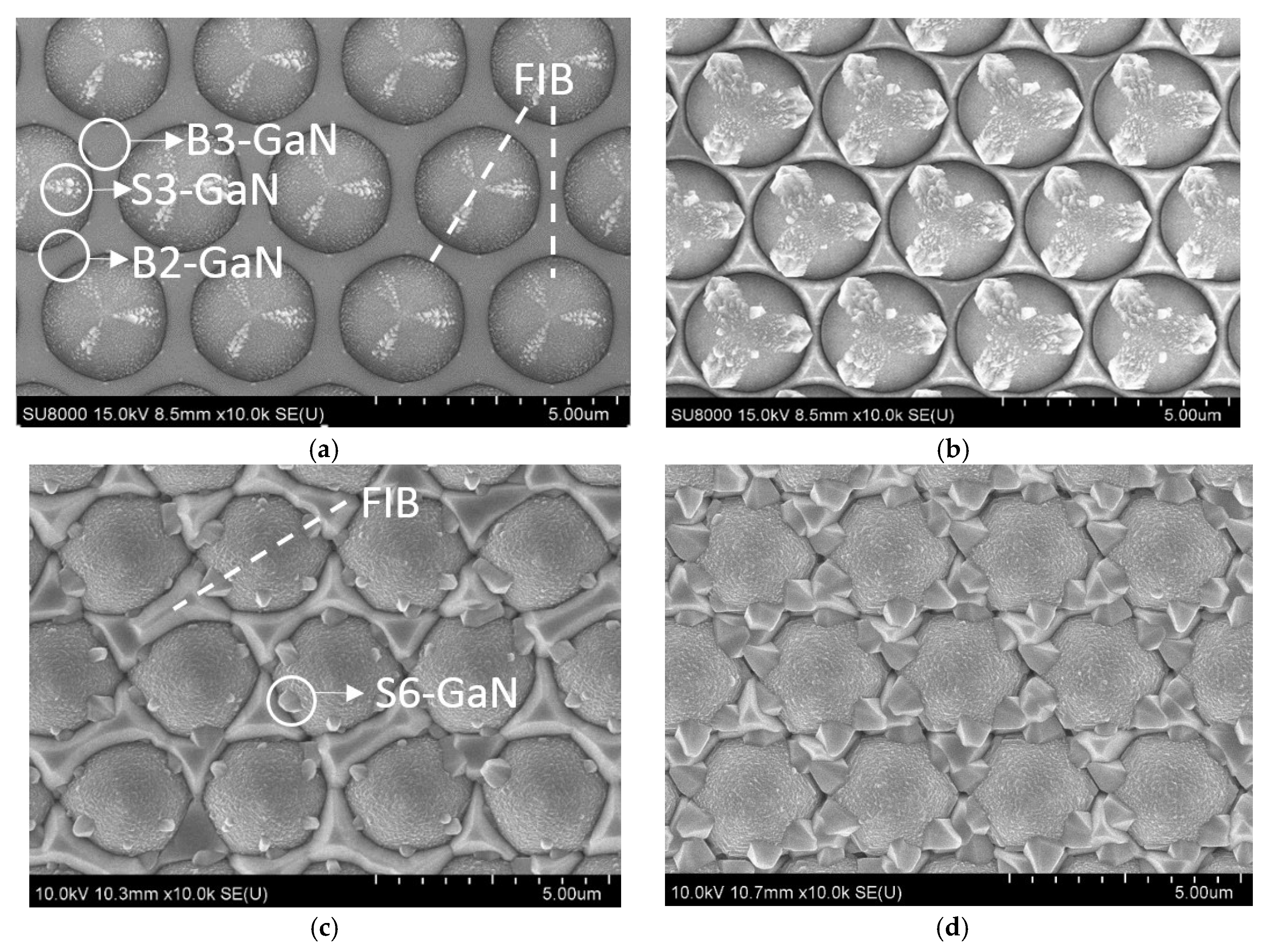
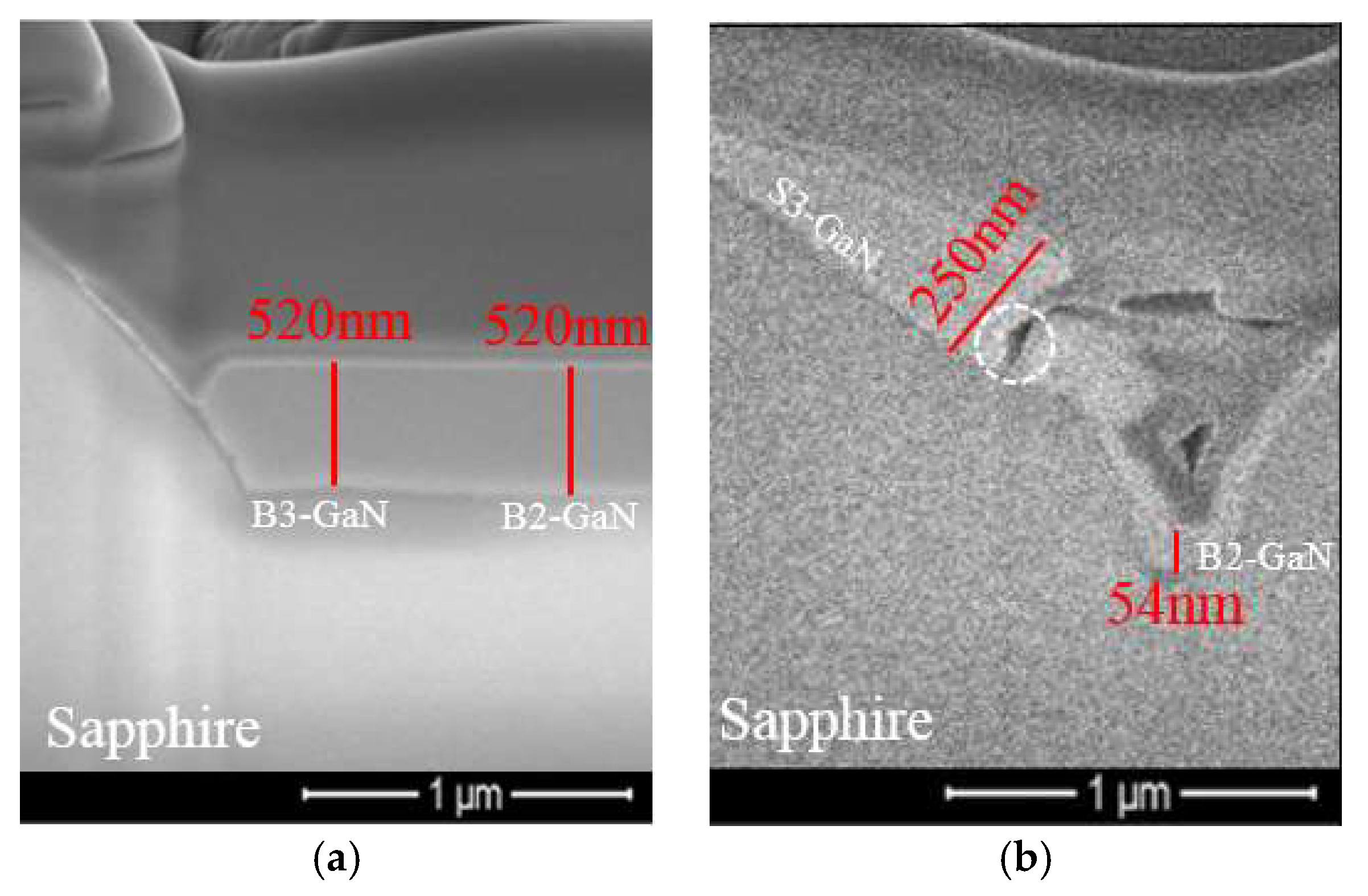
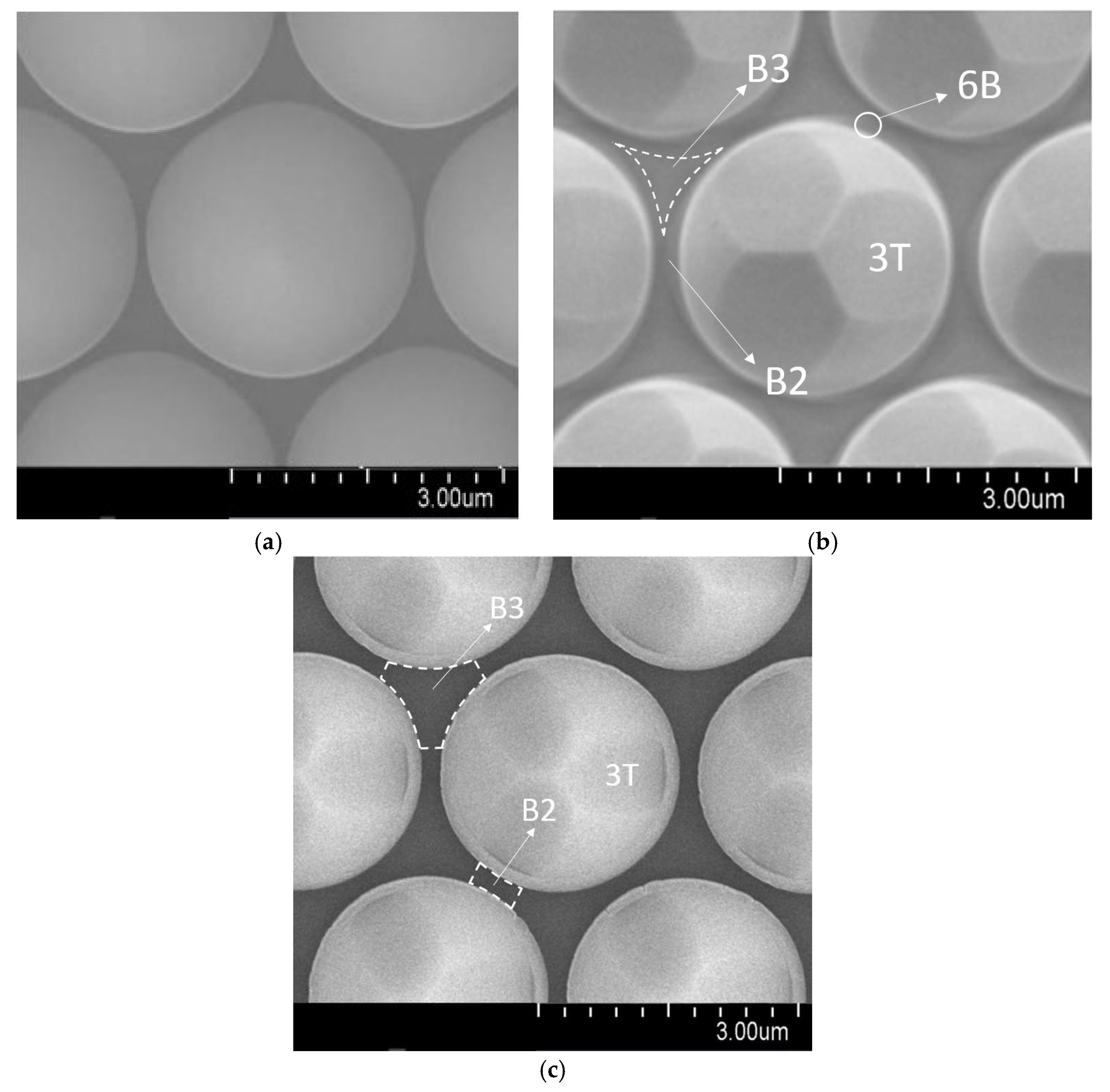
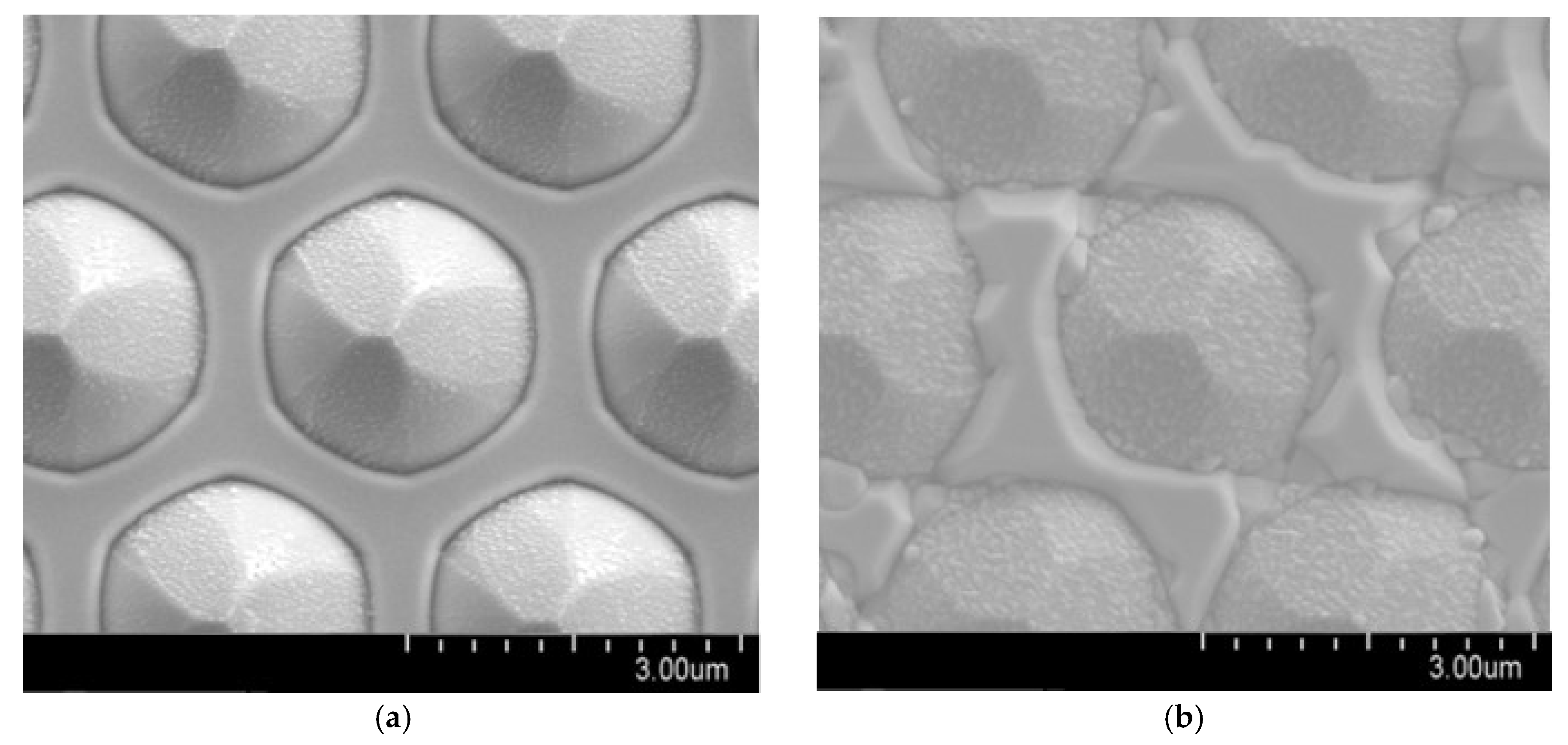
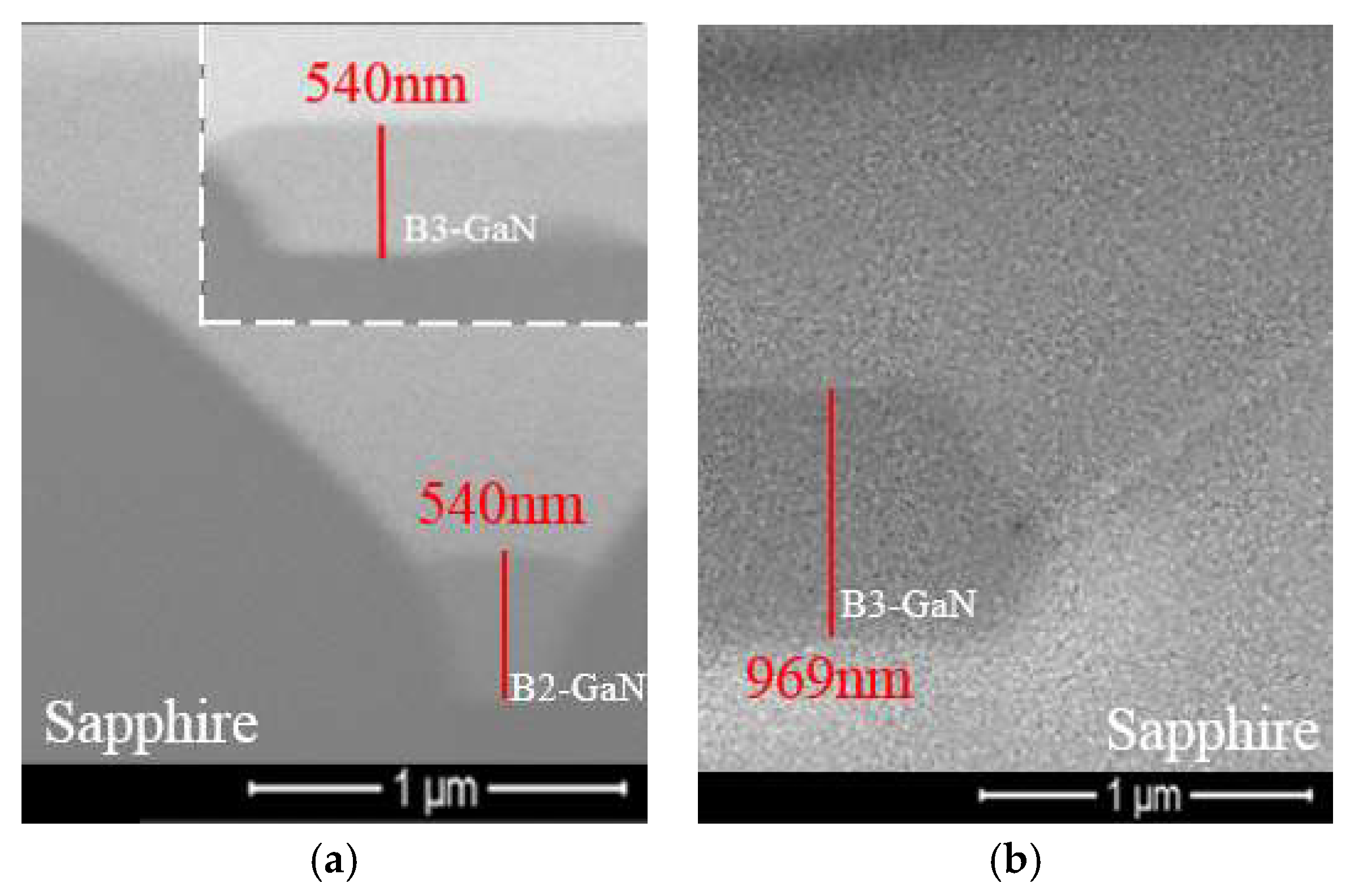
In this study, commercial dry etching c-plane micron-sized PSS (2.8 μm width and 0.2 μm spacing) was modified. As shown in Figure 1, two kinds of PSS samples were used to investigate the effect of modification of micron-sized PSS patterns on the GaN growth mechanism: (1) RPSS (regular PSS without etching) and (2) PSSE (RPSS etched in sulfuric–phosphoric acid (ratio 3:1) at 270 °C for 30 s). As shown in Figure 1b, 3T {1 1 ¯ 05} facets were observed on the pattern of PSSE [19,20,21,22,23].
Two kinds of nucleation layers (NL) were used: (1) ex-situ AlN NL and (2) in-situ GaN NL. To fabricate ex-situ AlN NL, 40 nm AlN was deposited by RF-sputter system using Al target in N2 gas at 650 °C. As for the in-situ GaN NL, an in-situ 25-nm-thick low-temperature GaN layer was deposited at 550 °C by MOCVD.
As shown in Table 1, four kinds of micron-sized PSS samples were then used to investigate the effect of modification of PSS patterns on the GaN growth mechanism: (1) AlNR (RPSS with AlN NL); (2) AlNE (PSSE with AlN NL); (3) GaNR (RPSS with GaN NL); and (4) GaNE (PSSE with GaN NL).
To investigate the GaN epitaxial behavior, high-temperature undoped GaN (HTU-GaN) was grown by MOCVD at 1060 °C with chamber pressure of 200 torr (26,664 Pa) for 2 min.

3. Results

Figure 2 shows the surface morphologies of micron-sized PSS after GaN was grown. The morphologies of bottom GaN (B-GaN) and sidewall GaN (S-GaN) were different. There were two kinds of B-GaN: (1) B3-GaN (GaN grown among three micron-sized patterns) and (2) B2-GaN (GaN grown between two patterns). Two kinds of S-GaN were found: (1) S3-GaN (with AlN as NL; Figure 2a) and (2) S6-GaN (with GaN as NL; Figure 2c). To measure the thicknesses of B-GaN and S-GaN, cross-sectional SEM was carried out by focused ion beam (FIB) cutting along the dash lines as shown in Figure 2a,c. Some of the related images are shown in Figure 3, and the measured maximum thicknesses are summarized in Table 2.

4. Discussion

A simple treatment of the MOCVD thin-film growth kinetic involves mass transport and reaction [24,25]. It is reasonable to assume that the mass transport was the same for all the samples as GaN was grown in the same conditions.
In a reaction between A and B to give products C and D, the following applies according to the balance equation:
a A + b B → c C + d D
The reaction is related to the reactant concentrations in the following way:
Rate = K [A]x[B]y
where K is the rate constant; the numbers x and y are partial orders of reaction.
In this case, there were four surface reaction constants: (1) sidewall with AlN (KSAlN), (2) bottom with AlN (KBAlN), (3) sidewall with GaN (KSGaN), and (4) bottom with GaN (KBGaN).

4.1. Ex-Situ AlN as NL

When ex-situ AlN NL was used, as shown in Figure 2a, two kinds of GaN were found on AlNR. B-GaN was initiated from the bottom c-plane as expected, while S-GaN (S3-GaN) was from sidewall surfaces, which has been reported earlier [14,15,26,27]. Both B-GaN and S3-GaN were Wurtzite structures. The orientation relationship between GaN (including B-GaN and S3-GaN) and sapphire was established as (0001)GaN // (0001) sapphire and [1 1 ¯ 00]GaN // [11 2 ¯ 0]sapphire.
As shown in Figure 3a, no void was found among GaN crystals as there was no coalescence yet between S-GaN and B-GaN.
Table 2 and Figure 3a show that the maximum thicknesses of B3-GaN (HB3-GaN) and B2-GaN (HB2-GaN) of AlNR were around 520 nm, which was much thicker than that of S3-GaN (HS3-GaN, 74 nm), indicating that KBAlN was much greater than KS3AlN [26].
However, with the modification of PSS patterns (AlNE), HS3-GaN of AlNE did not diminish but increased. As shown in Figure 2b and Figure 3b, and Table 2, compared with AlNR, the HS3-GaN of AlNE increased from 74 to 250 nm. At the same time, HB3-GaN decreased from 520 to 136 nm, and HB2-GaN decreased from 520 to 54 nm.
Moreover, as shown in Figure 3b, irregular voids (circled with dashed lines) were observed between S3-GaN and B2-GaN. These voids were created during the coalescence of GaN crystals [17].
This observation suggested that instead of reducing the reaction constant of S3-GaN (KS3AlN), modification of PSS patterns (AlNE) enhanced KSAlN and reduced KBAlN. As KBAlN should be a constant, we believe this KBAlN reduction should have been caused by the change in the area of the bottom c-plane.
Figure 4 is the high magnifications of (a) RPSS and (b) PSSE. In addition to sidewall facets, an extra six 6B {3 4 ¯ 17} facets were found on the bottom of patterns of PSSE [28], as shown in Figure 4b. The appearance of 6B facets reduced the bottom c-plane fraction as determined by estimating the B3 (B2) vs. total area on the SEM images.
Compared with RPSS, B3 fraction of PSSE reduced from 18% to 12%, while B2 fraction reduced from 3% to 0 %. This reduction of bottom c-plane made epitaxy of GaN film on PSSE very difficult [29]. Consequently, it appeared that the KBAlN of AlNE was much less than that of AlNR.
In addition, compared with AlNR, HS3-GaN of AlNE increased from 74 to 250 nm, as shown in Figure 2b and Figure 3b and Table 2. This is because the consuming of the reactants in front of the bottom c-plane can affect reactant concentrations in front of the sidewall. As shown in Figure 4, the distance between the sidewall and the bottom c-plane was only around 1 µm. As the growth rate of AlNE was much smaller than that of AlNR, the formation of B-GaN of AlNE would consume only a small portion of the reactants. As a result, the reactant concentrations in front of the sidewall of AlNE were increased. Consequently, HS3-GaN of AlNE was thicker than that of AlNR.

4.2. In-Situ GaN as NL

When in-situ GaN NL was used, as shown in Figure 2c, two kinds of GaN were found on AlNR: (1) B-GaN and (2) S6-GaN [13,14,15,16]. They were both Wurtzite structures, and the orientation relationship between GaN and sapphire was established as (0001)GaN // (0001) sapphire and [1 1 ¯ 00]GaN // [11 1 ¯ 0]sapphire.
Table 2 and Figure 3c show that HB3-GaN and HB2-GaN of GaNR were 1261 nm and 776 nm, respectively. Their thicknesses were much greater than HS6-GaN (371 nm) [14,27]. In other words, KBGaN was much greater than KS6GaN.
We also found that modification of PSS patterns (PSSE) did not diminish the growth of sidewall GaN (S6-GaN). Compared with GaNR, HS6-GaN of GaNE increased from 371 to 614 nm. At the same time, HB3-GaN decreased from 1261 to 616 nm, and HB2-GaN decreased from 776 to 157 nm, as shown in Figure 2 and Table 2. We believe that these thickness changes were also due to the reduction in the bottom c-plane of GaNE.
In both cases, beside voids between S3-GaN and B2-GaN (circled with dashed lines), voids were also found between B3-GaN and B2-GaN (squared with dashed lines). These voids were created during the coalescence of GaN crystals [17].

4.3. Bottom C-Plane Protection

To avoid the reduction of the bottom c-plane areas of micron-sized PSS, the bottom c-plane was protected by SiO2 and then etched with sulfuric–phosphoric acid. This was designated as PSSO. Figure 5 shows the PSSO fabrication processes. Micron-sized RPSS was first deposited with 200-nm-thick SiO2 film (Figure 5a). A photoresist (PR) layer was spun onto the surface to protect the bottom oxide (B-OX). Sidewall oxide (S-OX) and PR were then removed, as shown in Figure 5b,c. Samples were etched in sulfuric–phosphoric acid at 270 °C for 30 s. B-oxide was then removed (Figure 5e).
Figure 4c is the high magnification of the PSSO surface. Only sidewall 3T facets were found, and no 6B facets were observed. Compared with RPSS, B3 fraction and B2 fraction were the same as those of RPSS. There was no reduction in the bottom c-plane areas of micron-sized PSSO.
Two kinds of PSSO samples were then fabricated to investigate the growth mechanism of GaN: (1) AlNOE (PSSO with AlN NL) and (2) GaNOE (PSSO with GaN NL).
As shown in Table 2 and Figure 6, no S3-GaN was grown from AlNOE, and no S6-GaN was grown from GaNOE either. In both case, no void was found among GaN crystals, as shown in Figure 7.

5. Conclusions

In this study, the growth of sidewall GaN was successfully suppressed by modifying the surface of micron-sized PSS. Sulfuric–phosphoric acid was used to modify the surface of dry etching c-plane PSS. Two kinds of nucleation layers—ex-situ AlN NL and in-situ GaN NL—were introduced prior to growth of GaN epilayer.
After etching, three 3T {1 1 ¯ 05} facets were found on the pattern sidewall. At the same time, six 6B {3 4 ¯ 17} facets were observed on the bottom of the patterns. The appearance of 6B facets reduced the bottom c-plane fraction, which made epitaxy of GaN on bottom c-plane very difficult. Consequently, instead of reducing the growth of sidewall GaN, this modification appeared to enhance the growth of GaN from the sidewall of the patterns.
A 200-nm-thick SiO2 film was used to protect the bottom c-plane areas. After etching, only sidewall 3T facets were observed, and no 6B facet appeared. The bottom c-plane areas did not reduce. As a result, sidewall GaN was successfully suppressed in both NL systems.

Author Contributions

Conceptualization, W.-Y.H. and Y.S.W.; Formal analysis, Y.-C.L., P.-Y.W., W.-M.Y., K.-L.L. and Y.S.W.; Investigation, W.-Y.H., Y.-C.L., P.-Y.W., W.-M.Y., J.-K.S. and Y.S.W.; Methodology, W.-Y.H.; Project administration, Y.S.W.; Writing—original draft, W.-Y.H.; Writing—review & editing, Y.S.W.

Funding

This research was funded by (1) the National Science Council of the Republic of China under Grant No. MOST105-2221-E-009-051-MY3, (2) the Ministry of Science and Technology, under Grant No. MOST107-3017-F-009-002, and (3) the “Center for Semiconductor Technology Research” from The Featured Areas Research Center Program within the framework of the Higher Education Sprout Project by the Ministry of Education (MOE) in Taiwan.

Acknowledgments

Technical support from the National Nano Device Laboratory, Center for Nano Science and Technology, Nano Facility Center, and Semiconductor Laser Technology Laboratory of the National Chiao Tung University are also acknowledged.

Conflicts of Interest

The authors declare no conflict of interest.

References

  1. Mukai, T.; Nagahama, S.; Sano, M.; Yanamoto, T.; Morita, D.; Mitani, T.; Narukawa, Y.; Yamamoto, S.; Niki, I.; Yamada, M.; et al. Recent progress of nitride-based light emitting devices. Phys. Status Solidi A 2003, 200, 52–57. [Google Scholar] [CrossRef]
  2. Mukai, T.; Yamada, M.; Nakamura, S. Characteristics of InGaN-based UV/blue/green/amber/red light-emitting diodes. Jpn. J. Appl. Phys. 1999, 38, 3976–3981. [Google Scholar] [CrossRef]
  3. Amano, H.; Sawaki, N.; Akasaki, I.; Toyoda, Y. Metalorganic vapor phase epitaxial growth of a high quality GaN film using an AlN buffer layer. Appl. Phys. Lett. 1986, 48, 353–355. [Google Scholar] [CrossRef]
  4. Nakamura, S.; Mukai, T.; Senoh, M. In situ monitoring and Hall measurements of GaN grown with GaN buffer layers. J. Appl. Phys. 1992, 71, 5543–5549. [Google Scholar] [CrossRef]
  5. Wuu, D.S.; Wang, W.K.; Wen, K.S.; Huang, S.C.; Lin, S.H.; Horng, R.H.; Yu, Y.S.; Pan, M.H. Fabrication of pyramidal patterned sapphire substrates for high-efficiency InGaN-based light emitting diodes. J. Electrochem. Soc. 2006, 153, G765–G770. [Google Scholar] [CrossRef]
  6. Lee, J.H.; Oh, J.T.; Kim, Y.C.; Lee, J.H. Stress reduction and enhanced extraction efficiency of GaN-based LED grown on cone-shape-patterned sapphire. IEEE Photonics Technol. Lett. 2008, 20, 1563–1565. [Google Scholar] [CrossRef]
  7. Tsai, C.H.; Ma, M.H.; Yin, Y.F.; Li, H.W.; Lai, W.C.; Huang, J. Nanoscale epitaxial lateral overgrowth of GaN-based light-emitting diodes on an AlN nanorod-array template. IEEE J. Quantum Electron. 2015, 51, 2006–2009. [Google Scholar] [CrossRef]
  8. Lin, H.C.; Lin, R.S.; Chyi, J.I.; Lee, C.M. Light output enhancement of InGaN light-emitting diodes grown on Masklessly etched sapphire substrates. IEEE Photonics Technol. Lett. 2008, 20, 1621–1623. [Google Scholar] [CrossRef]
  9. Hsieh, C.-Y.; Lin, B.-W.; Cho, H.-J.; Wang, B.-M.; Sermon Wu, Y. Investigation of GaN Films Grown on Liquid-Phase Deposited SiO2 Nanopatterned Sapphire Substrates. ECS J. Solid State Sci. Technol. 2012, 1, Q35–Q37. [Google Scholar] [CrossRef]
  10. Lee, Y.J.; Hsu, T.C.; Kuo, H.C.; Wang, S.C.; Yang, Y.L.; Yen, S.N.; Chu, Y.T.; Shen, Y.J.; Hsieh, M.H.; Jou, M.J.; et al. Improvement in light-output efficiency of near-ultraviolet InGaN-GaN LEDs fabricated on stripe patterned sapphire substrate. Mater. Sci. Eng. B 2005, 122, 184–187. [Google Scholar] [CrossRef]
  11. Feng, Z.H.; Lau, K.M. Enhanced luminescence from GaN-based blue LEDs grown on grooved sapphire substrates. IEEE Photonics Technol. Lett. 2005, 17, 1812–1814. [Google Scholar] [CrossRef]
  12. Lee, Y.J.; Hsu, T.C.; Kuo, H.C.; Wang, S.C.; Yang, Y.L.; Yen, S.N.; Chu, Y.T.; Shen, Y.J.; Hsieh, M.H.; Jou, M.J.; et al. Enhancing the output power of GaN-based LEDs grown on wet-etched patterned sapphire substrates. IEEE Photonics Technol. Lett. 2006, 18, 1152–1154. [Google Scholar] [CrossRef]
  13. Zhou, S.; Hu, H.; Liu, X.; Liu, M.; Ding, X.; Gui, C.; Liu, S.; Guo, L.J. Comparative study of GaN-based ultraviolet LEDs grown on different-sized patterned sapphire substrates with sputtered AlN nucleation layer. Jpn. J. Appl. Phys. 2017, 56, 111001. [Google Scholar] [CrossRef]
  14. He, C.; Zhao, W.; Zhang, K.; He, L.; Wu, H.; Liu, N.; Zhang, S.; Liu, X.; Chen, Z. High-Quality GaN Epilayers Achieved by Facet-Controlled Epitaxial Lateral Overgrowth on Sputtered AlN/PSS Templates. ACS Appl. Mater. Interfaces 2017, 9, 43386–43392. [Google Scholar] [CrossRef] [PubMed]
  15. Hu, H.; Zhou, S.; Liu, X.; Gao, Y.; Gui, C.; Liu, S. Effects of GaN/AlGaN/Sputtered AlN nucleation layers on performance of GaN-based ultraviolet light-emitting diodes. Sci. Rep. 2017, 7, 1–10. [Google Scholar] [CrossRef] [PubMed]
  16. Chen, S.-W.; Yang, Y.; Wen, W.-C.; Li, H.; Lu, T.-C. Significant improvement of GaN crystal quality with ex-situ sputtered AlN nucleation layers. Int. Soc. Opt. Photonics 2016, 9768, 97681D. [Google Scholar] [CrossRef]
  17. Chang, L.C.; Chen, Y.A.; Kuo, C.H. Spatial correlation between efficiency and crystal structure in GaN-based light-emitting diodes prepared on high-aspect ratio patterned sapphire substrate with sputtered AlN nucleation layer. IEEE Trans. Electron Devices 2014, 61, 2443–2447. [Google Scholar] [CrossRef]
  18. Lai, W.C.; Yen, C.H.; Yang, Y.Y.; Wang, C.K.; Chang, S.J. GaN-Based ultraviolet light emitting diodes with Ex situ sputtered AlN nucleation layer. IEEE/OSA J. Disp. Technol. 2013, 9, 895–899. [Google Scholar] [CrossRef]
  19. Chen, Y.-C.; Hsiao, F.-C.; Lin, B.-W.; Wang, B.-M.; Sermon Wu, Y.; Hsu, W.-C. The Formation and the Plane Indices of Etched Facets of Wet Etching Patterned Sapphire Substrate. J. Electrochem. Soc. 2012, 159, D362. [Google Scholar] [CrossRef]
  20. Shen, J.; Zhang, D.; Wang, Y.; Gan, Y. AFM and SEM Study on Crystallographic and Topographical Evolution of Wet-Etched Patterned Sapphire Substrates (PSS). ECS J. Solid State Sci. Technol. 2017, 6, R24–R34. [Google Scholar] [CrossRef]
  21. Shen, J.; Zhang, D.; Wang, Y.; Gan, Y. AFM and SEM Study on Crystallographic and Topographical Evolution of Wet-Etched Patterned Sapphire Substrates (PSS). ECS J. Solid State Sci. Technol. 2017, 6, R122–R130. [Google Scholar] [CrossRef]
  22. Shen, J.; Zhang, D.; Wang, Y.; Gan, Y. AFM and SEM Study on Crystallographic and Topographical Evolution of Wet-Etched Patterned Sapphire Substrates (PSS). ECS J. Solid State Sci. Technol. 2017, 6, R163–R169. [Google Scholar] [CrossRef]
  23. Lee, Y.J.; Chiu, C.H.; Kuo, H.C.; Lu, T.C.; Wang, S.C.; Ng, K.W.; Lau, K.M.; Yang, Z.P.; Chang, S.P.; Lin, S.Y. Simultaneously enhancing internal and extraction efficiencies of GaN-based light emitting diodes via chemical-wet-etching patterned-sapphire-substrate (CWE-PSS). ECS Trans. 2007, 11, 225–230. [Google Scholar] [CrossRef]
  24. Plummer, J.D.; Deal, M.D.; Griffin, P.B. Silicon VLSI Technology Fundamentals, Practice and Modeling, 1st ed.; Prentice Hall: Upper Saddle River, NJ, USA, 2000; p. 514. [Google Scholar]
  25. Ravasio, S.; Momose, T.; Fujii, K.; Shimogaki, Y.; Sugiyama, M.; Cavallotti, C. Analysis of the gas phase kinetics active during GaN deposition from NH3 and Ga(CH3)3. J. Phys. Chem. A 2015, 119, 7858–7871. [Google Scholar] [CrossRef] [PubMed]
  26. Wu, P.-Y.; Li, J.-H.; Hsu, L.-H.; Huang, C.-Y.; Cheng, Y.-J.; Kuo, H.-C.; Wu, Y.S. Effect of Sputtered AlN Location on the Growth Mechanism of GaN. ECS J. Solid State Sci. Technol. 2017, 6, R131–R134. [Google Scholar] [CrossRef]
  27. Shang, L.; Zhai, G.; Mei, F.; Jia, W.; Yu, C.; Liu, X.; Xu, B. The effect of nucleation layer thickness on the structura evolution and crystal quality of bulk GaN grown by a two-step process on cone-patterned sapphire substrate. J. Cryst. Growth 2016, 442, 89–94. [Google Scholar] [CrossRef]
  28. Hsueh, H.H.; Ou, S.L.; Cheng, C.Y.; Wuu, D.S.; Horng, R.H. Performance of InGaN light-emitting diodes fabricated on patterned sapphire substrates with modified top-tip cone shapes. Int. J. Photoenergy 2014. [Google Scholar] [CrossRef]
  29. Chen, C.-C.; Hsiao, F.C.; Lin, B.-W.; Hsu, W.-C.; Wu, Y.S. Evolution of Bottom c-Plane on Wet-Etched Patterned Sapphire Substrate. ECS J. Solid State Sci. Technol. 2013, 2, R169–R171. [Google Scholar] [CrossRef]
Figure 1. SEM images of (a) RPSS (regular patterned sapphire substrates) and (b) PSSE (RPSS etched in sulfuric–phosphoric acid).
Micromachines 09 00622 g001
Figure 2. SEM images of GaN grown on (a) AlNR, (b) AlNE, (c) GaNR, and (d) GaNE.
Micromachines 09 00622 g002
Figure 3. Cross-sectional SEM images from Figure 2. (a) AlNR, (b) AlNE, (c) GaNR, and (d) GaNE.
Micromachines 09 00622 g003aMicromachines 09 00622 g003b
Figure 4. The high magnification SEM images of (a) RPSS, (b) PSSE, and (c) PSSO.
Micromachines 09 00622 g004
Figure 5. The flow charts of PSSO fabrication processes.
Micromachines 09 00622 g005
Figure 6. SEM images of GaN grown on (a) AlNOE and (b) GaNOE.
Micromachines 09 00622 g006
Figure 7. Cross-sectional SEM images from Figure 6. (a) AlNOE and (b) GaNOE.
Micromachines 09 00622 g007
Table 1. Summary of sample preparation parameters.
SampleAlNRAlNEGaNRGaNEAlNOEGaNOE
Nucleation layers (NL)AlNAlNGaNGaNAlNGaN
PSS substrateRPSSPSSERPSSPSSEPSSOPSSO
Table 2. The measured maximum thicknesses of GaN.
ThicknessGaN TypeAlNRAlNEAlNOEGaNRGaNEGaNOE
Thickness (nm)HB3-GaN5201365401261616969
HB2-GaN52054540776157951
HS3-GaN742500000
HS6-GaN0003716410

