Development, Modeling, Fabrication, and Characterization of a Magnetic, Micro-Spring-Suspended System for the Safe Electrical Interconnection of Neural Implants

Abstract
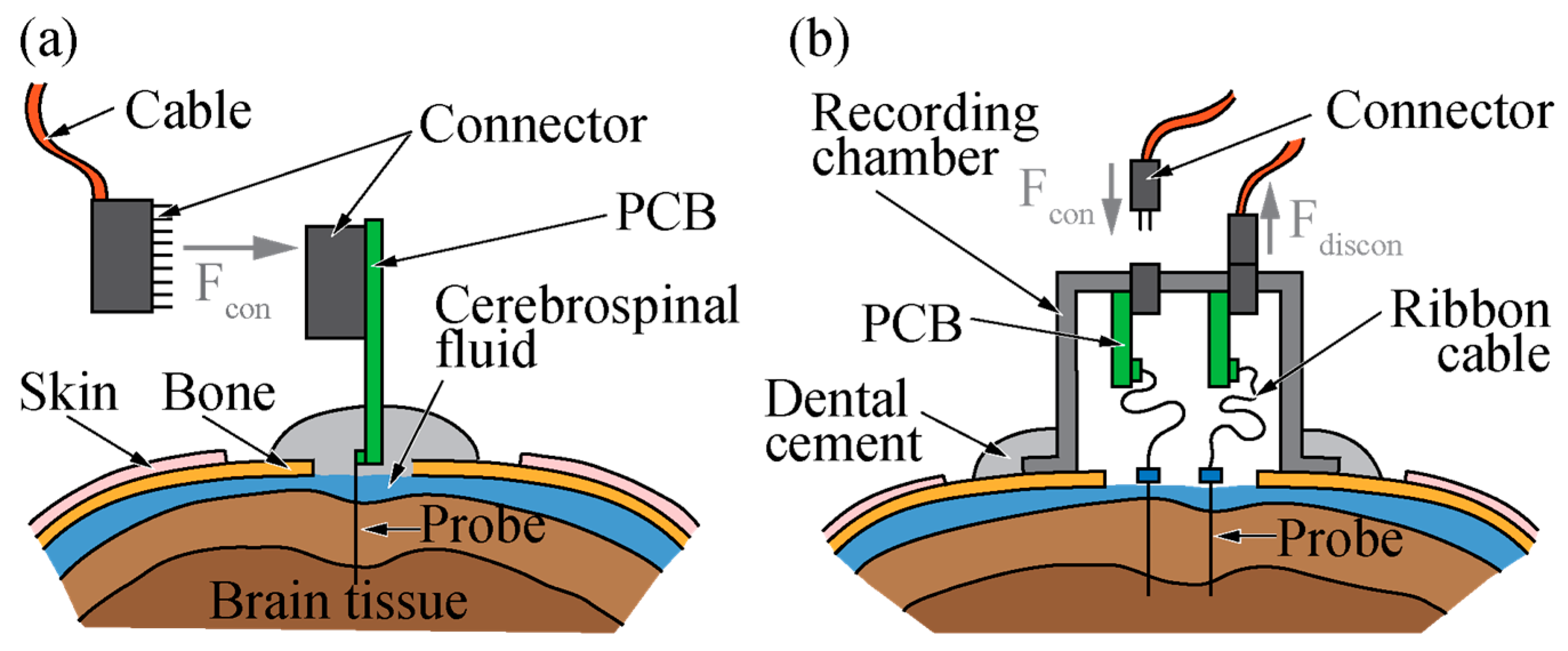
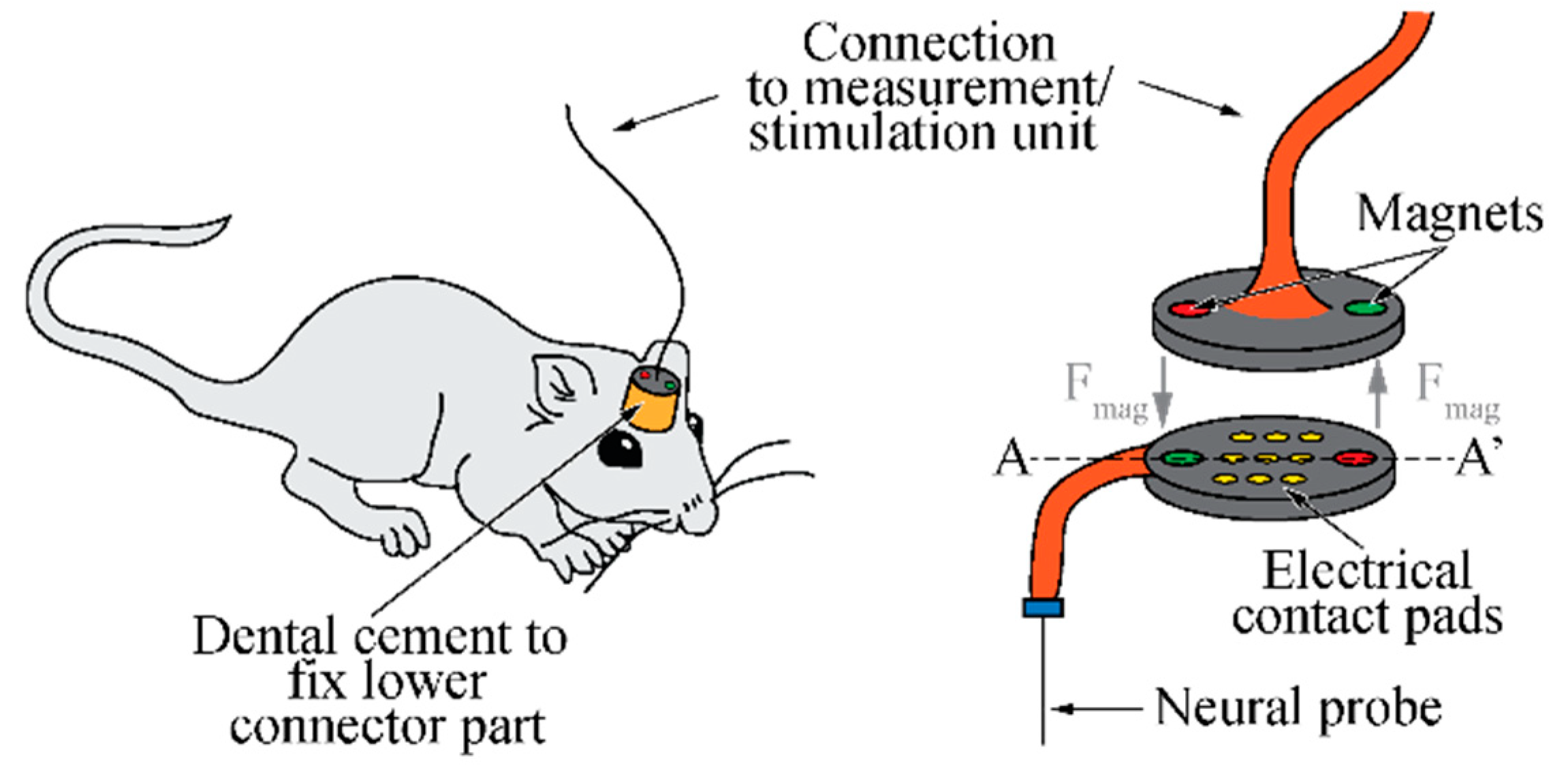
:1. Introduction
2. Materials and Methods
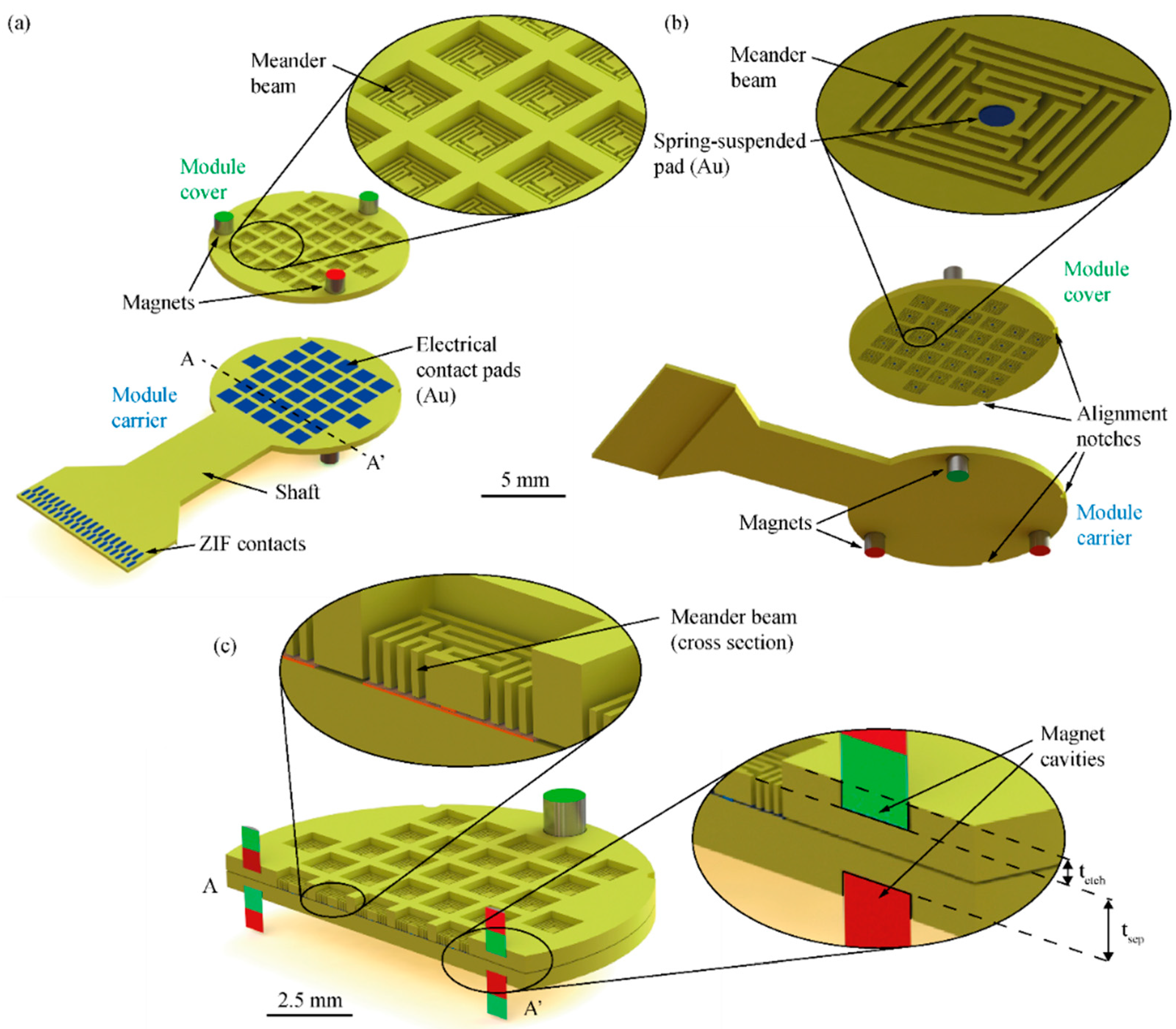
2.1. Module Design
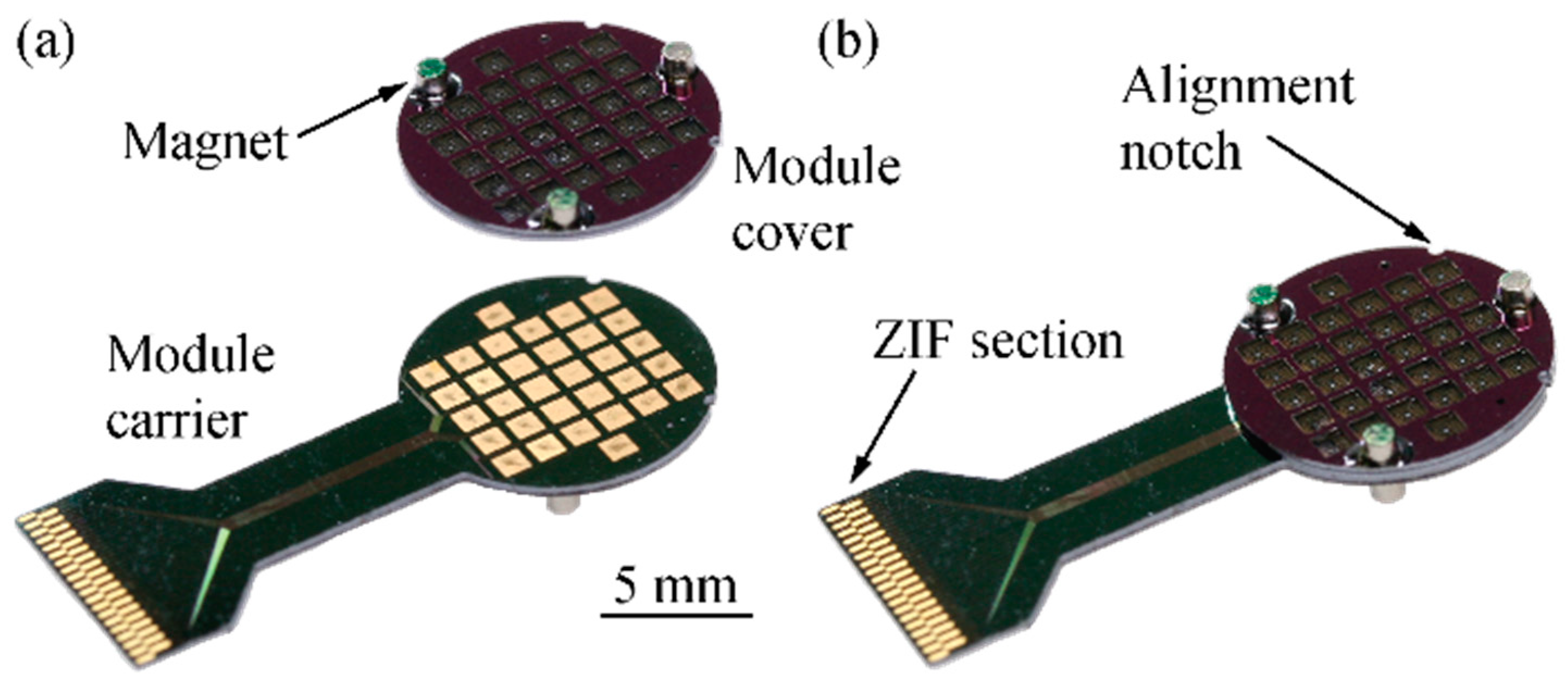
2.2. Module Fabrication
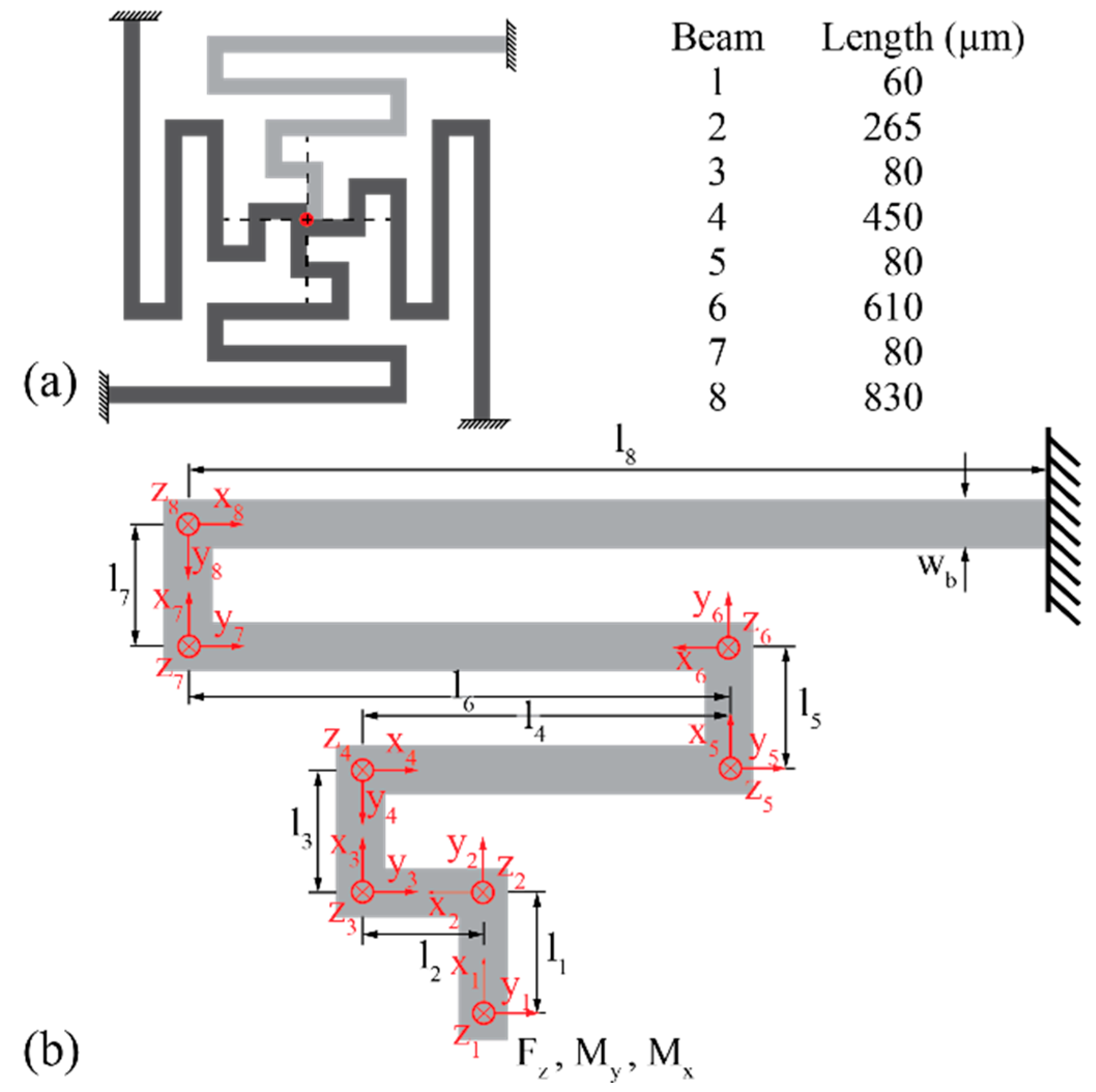
2.3. Modeling of Spring-Suspended Contact Pads
2.3.1. Analytical Model
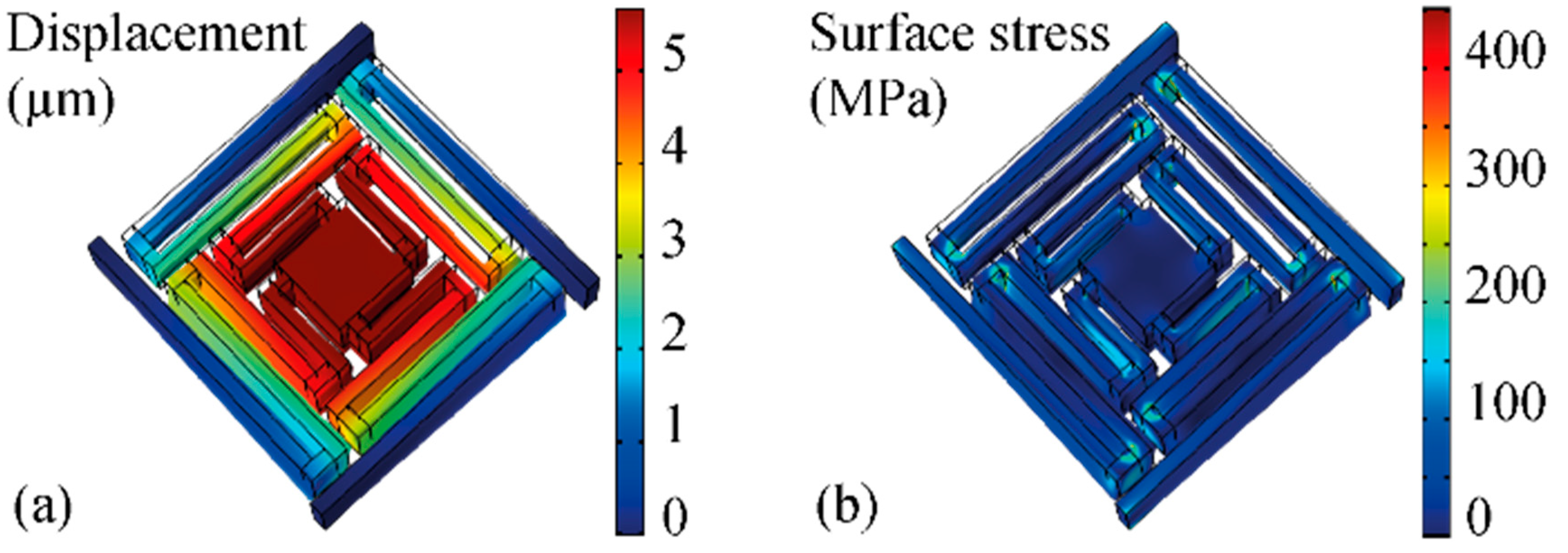
2.3.2. Finite Element Simulations
2.4. Module Characterization
2.4.1. Mechanical Tests
2.4.2. Electrical Tests
3. Results
3.1. Module Fabrication
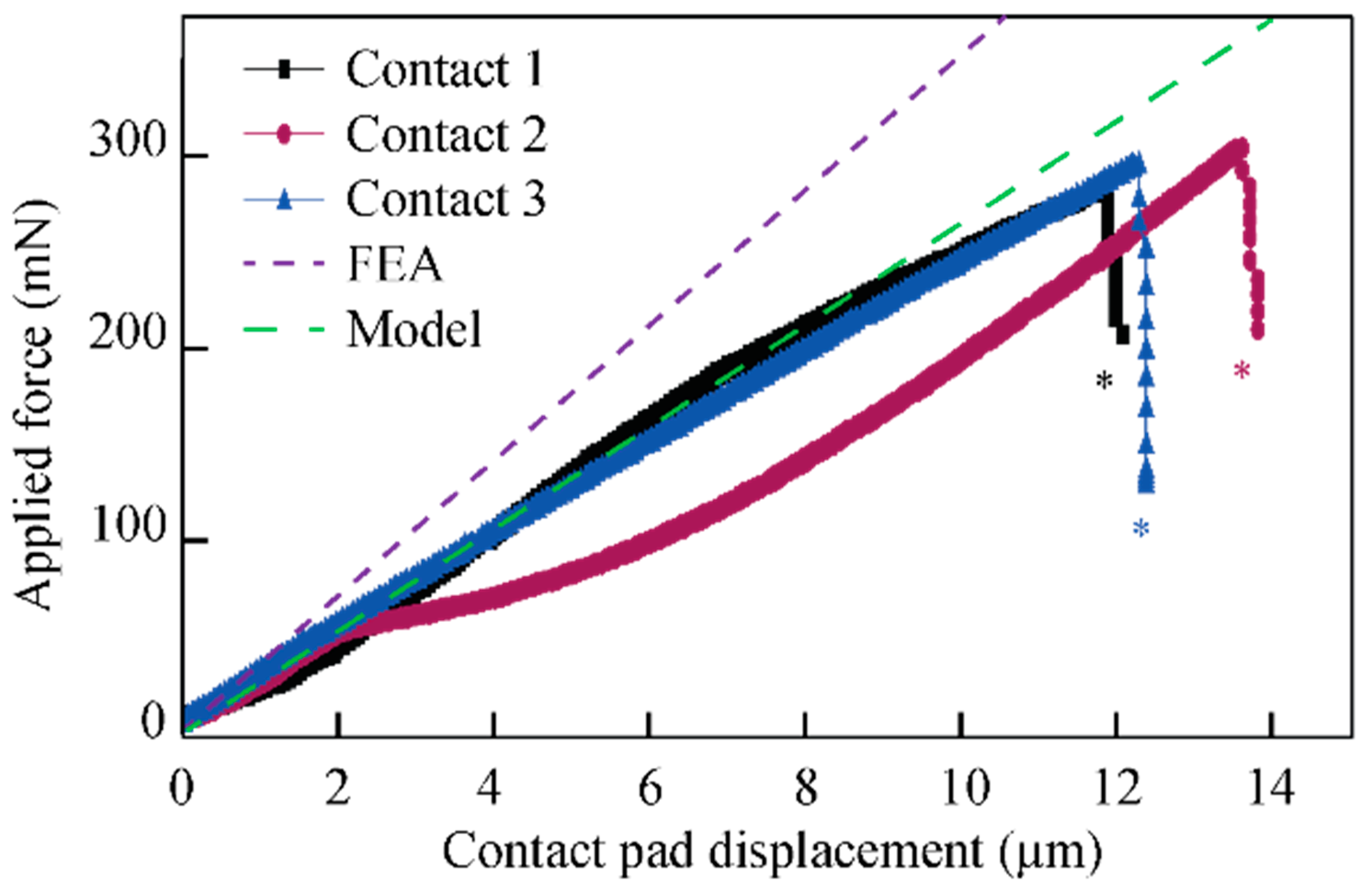
3.2. Modeling
3.3. Module Characterization
4. Discussion
5. Conclusions
Author Contributions
Funding
Acknowledgments
Conflicts of Interest
References
- Limousin, P.; Krack, P.; Pollak, P.; Benazzouz, A.; Ardouin, C.; Hoffmann, D.; Benabid, A.-L. Electrical stimulation of the subthalamic nucleus in advanced Parkinson’s disease. N. Engl. J. Med. 1998, 339, 1105–1111. [Google Scholar] [CrossRef] [PubMed]
- Duncan, J.S. Epilepsy surgery. Clin. Med. 2007, 7, 137–142. [Google Scholar] [CrossRef] [Green Version]
- Schulze-Bonhage, A.; Zentner, J. The preoperative evaluation and surgical treatment of epilepsy. Dtsch. Arztebl. Int. 2014, 111, 313–319. [Google Scholar] [CrossRef] [PubMed]
- Bittar, R.G.; Yianni, J.; Wang, S.; Liu, X.; Nandi, D.; Joint, C.; Scott, R.; Bain, P.G.; Gregory, R.; Stein, J.; et al. Deep brain stimulation for generalised dystonia and spasmodic torticollis. J. Clin. Neurosci. 2005, 12, 12–16. [Google Scholar] [CrossRef] [PubMed]
- Roche, J.P.; Hansen, M.R. On the horizon: Cochlear implant technology. Otolaryngol. Clin. N. Am. 2015, 48, 1097–1116. [Google Scholar] [CrossRef] [PubMed]
- Zierhofer, C.M.; Hochmair-Desoyer, I.J.; Hochmair, E.S. Electronic design of a cochlear implant for multichannel high-rate pulsatile stimulation strategies. IEEE Trans. Rehabil. Eng. 1995, 3, 112–116. [Google Scholar] [CrossRef]
- Da Cruz, L.; Coley, B.F.; Dorn, J.; Merlini, F.; Filley, E.; Christopher, P.; Chen, F.K.; Wuyyuru, V.; Sahel, J.; Stanga, P.; et al. The Argus II epiretinal prosthesis system allows letter and word reading and long-term function in patients with profound vision loss. Br. J. Ophthalmol. 2013, 97, 632–636. [Google Scholar] [CrossRef] [PubMed] [Green Version]
- Rathbun, D.L.; Jalligampala, A.; Stingl, K.; Zrenner, E. To what extent can retinal prostheses restore vision? In Proceedings of the 7th International IEEE/EMBS Conference on Neural Engineering (NER), Montpellier, France, 22–24 April 2015; pp. 244–247. [Google Scholar] [CrossRef]
- Berényi, A.; Somogyvári, Z.; Nagy, A.J.; Roux, L.; Long, J.D.; Fujisawa, S.; Stark, E.; Leonardo, A.; Harris, T.D.; Buzsáki, G. Large-scale, high-density (up to 512 channels) recording of local circuits in behaving animals. J. Neurophysiol. 2014, 111, 1132–1149. [Google Scholar] [CrossRef]
- Pothof, F.; Bonini, L.; Lanzilotto, M.; Livi, A.; Fogassi, L.; Orban, G.A.; Paul, O.; Ruther, P. Chronic neural probe for simultaneous recording of single-unit, multi-unit, and local field potential activity from multiple brain sites. J. Neural. Eng. 2016, 13, 046006. [Google Scholar] [CrossRef] [PubMed] [Green Version]
- Donoghue, J.P.; Nurmikko, A.; Black, M.; Hochberg, L.R. Assistive technology and robotic control using motor cortex ensemble-based neural interface systems in humans with tetraplegia. J. Physiol. 2007, 579, 603–611. [Google Scholar] [CrossRef] [PubMed] [Green Version]
- Bonini, L.; Maranesi, M.; Livi, A.; Fogassi, L.; Rizzolatti, G. Space-dependent representation of objects and other’s action in monkey ventral premotor grasping neurons. J. Neurosci. 2014, 34, 4108–4119. [Google Scholar] [CrossRef] [PubMed]
- Gierthmuehlen, M.; Wang, X.; Gkogkidis, A.; Henle, C.; Fischer, J.; Fehrenbacher, T.; Kohler, F.; Raab, M.; Mader, I.; Kuehn, C.; et al. Mapping of sheep sensory cortex with a novel microelectrocorticography grid. J. Comp. Neurol. 2014, 522, 3590–3608. [Google Scholar] [CrossRef] [PubMed]
- Ulyanova, A.V.; Koch, P.F.; Grovola, M.R.; Browne, K.D.; Russo, R.J.; Adam, C.D.; Smith, D.H.; Chen, H.I.; Johnson, V.E.; Cullen, D.K.; et al. Electrophysiological signature reveals laminar structure of the porcine hippocampus. bioRxiv 2017, 1, 201285. [Google Scholar] [CrossRef]
- Brochier, T.; Zehl, L.; Hao, Y.; Duret, M.; Sprenger, J.; Denker, M.; Grün, S.; Riehle, A. Massively parallel recordings in macaque motor cortex during an instructed delayed reach-to-grasp task. Sci. Data 2018, 5, 180055. [Google Scholar] [CrossRef] [PubMed]
- Kohler, F.; Gkogkidis, C.A.; Bentler, C.; Wang, X.; Gierthmuehlen, M.; Fischer, J.; Stolle, C.; Reindl, L.M.; Rickert, J.; Stieglitz, T.; et al. Closed-loop interaction with the cerebral cortex: A review of wireless implant technology. Brain Comput. Interface 2017, 4, 146–154. [Google Scholar] [CrossRef]
- Fiedler, E.; Ordonez, J.; Stieglitz, T. Modular assembly of flexible thin-film electrode arrays enabled by a laser-structured ceramic adapter. In Proceedings of the 6th International IEEE/EMBS Conference on Neural Engineering (NER), San Diego, CA, USA, 6–8 November 2013; pp. 657–660. [Google Scholar] [CrossRef]
- Rubehn, B.; Bosman, C.; Oostenveld, R.; Fries, P.; Stieglitz, T. A MEMS-based flexible multichannel ECoG-electrode array. J. Neural Eng. 2009, 6, 036003. [Google Scholar] [CrossRef] [PubMed]
- Bernstein, J.G.; Allen, B.D.; Guerra, A.A.; Boyden, E.S. Processes for design, construction and utilisation of arrays of light-emitting diodes and light-emitting diode-coupled optical fibres for multi-site brain light delivery. J. Eng. 2015, 2015. [Google Scholar] [CrossRef] [PubMed]
- Barz, F.; Livi, A.; Lanzilotto, M.; Maranesi, M.; Bonini, L.; Paul, O.; Ruther, P. Versatile, modular 3D microelectrode arrays for neuronal ensemble recordings: From design to fabrication, assembly, and functional validation in non-human primates. J. Neural Eng. 2017, 14, 036010. [Google Scholar] [CrossRef] [PubMed]
- Data Sheet Omnetics Nano Series. Available online: http://www.omnetics.com/products/micro-and-nano-strips/nano-nps-npd-series#1852-tab4 (accessed on 4 June 2018).
- Wise, K.D.; Sodagar, A.M.; Yao, Y.; Gulari, M.N.; Perlin, G.E.; Najafi, K. Microelectrodes, microelectronics, and implantable neural microsystems. Proc. IEEE 2008, 96, 1184–1202. [Google Scholar] [CrossRef]
- Ordonez, J.; Schuettler, M.; Boehler, C.; Boretius, T.; Stieglitz, T. Thin films and microelectrode arrays for neuroprosthetics. MRS Bull. 2012, 37, 590–598. [Google Scholar] [CrossRef]
- Luan, L.; Wei, X.; Zhao, Z.; Siegel, J.J.; Potnis, O.; Tuppen, C.A.; Lin, S.; Kazmi, S.; Fowler, R.A.; Holloway, S.; et al. Ultraflexible nanoelectronic probes form reliable, glial scar-free neural integration. Sci. Adv. 2017, 3, 1601966. [Google Scholar] [CrossRef] [PubMed]
- News for “Break Away” Power Cords on Electric Deep Fryers. Available online: http://www.dowell.com.hk/breakawaycord_news.htm (accessed on 6 May 2017).
- Rohrbach, M.D.; Doutt, M.E.; Andre, B.K.; Lim, K.; DiFonzo, J.C.; Gery, J.-M. Magnetic Connector for Electronic Device. U.S. Patent 7,311,526, 25 December 2007. [Google Scholar]
- Kwon, K.Y.; Gnade, A.G.; Rush, A.D.; Patten, C.D. Head-mounted LED for optogenetic experiments of freely-behaving animal. In Proceedings of the SPIE BiOS, San Francisco, CA, USA, 13–18 February 2016; pp. 1–9. [Google Scholar] [CrossRef]
- Smith, C.F.; Guillory, K.S. High-Density, Low-mating-force, magnetically-coupled, percutaneous connector for implanted electrode arrays. In Proceedings of the 3rd International IEEE EMBS Conference on Neural Engineering, Kohala Coast, HI, USA, 2–5 May 2007; pp. 446–449. [Google Scholar] [CrossRef]
- Shah, K.G.; Lee, K.Y.; Tolosa, V.; Tooker, A.; Felix, S.; Benett, W.; Pannu, S. Chronic, percutaneous connector for electrical recording and stimulation with microelectrode arrays. In Proceedings of the 36th Annual International Conference of the IEEE Engineering in Medicine and Biology Society, Chicago, IL, USA, 26–30 August 2014; pp. 5240–5243. [Google Scholar] [CrossRef]
- Hoch, K.; Pothof, F.; Becker, F.; Paul, O.; Ruther, P. A Magnetic, micro-spring-suspended system for the safe electrical interconnection of neural implants. In Proceedings of the 31st IEEE International Conference on Micro Electro Mechanical Systems (MEMS), Belfast, UK, 21–25 January 2018; pp. 369–372. [Google Scholar] [CrossRef]
- Kim, B.J.; Kuo, J.T.W.; Hara, S.A.; Lee, C.D.; Yu, L.; Gutierrez, C.A.; Hoang, T.Q.; Pikov, V.; Meng, E. 3D parylene sheath neural probe for chronic recordings. J. Neural Eng. 2013, 10, 045002. [Google Scholar] [CrossRef] [PubMed]
- Herwik, S.; Paul, O.; Ruther, P. Ultrathin silicon chips of arbitrary shape by etching before grinding. J. Microelectromech. Syst. 2011, 20, 791–793. [Google Scholar] [CrossRef]
- Pilkey, W.D. Formulas for Stress, Strain, and Structural Matrices, 2nd ed.; John Wiley & Sons, Inc.: Hoboken, NJ, USA, 2005; pp. 619–660. ISBN 0-471-03221-2. [Google Scholar]
- Balke, H. Einführung in Die Technische Mechanik: Kinetik, 2nd ed.; Springer: Heidelberg, Germany, 2009; ISBN 978-3-540-89448-3. [Google Scholar]
- Balke, H. Einführung in Die Technische Mechanik: Festigkeitslehre, 3rd ed.; Springer: Heidelberg, Germany, 2014; ISBN 978-3-642-40980-6. [Google Scholar]
- Li, K.; Kasai, T.; Nakao, S.; Tanaka, H.; Ando, T.; Shikida, M.; Sato, K. A Method for measuring the fracture toughness of micrometer-sized single crystal silicon by tensile test. In Proceedings of the TRANSDUCERS ‘03 12th International Conference on Solid-State Sensors, Actuators and Microsystems, Boston, MA, USA, 8–12 June 2003; pp. 444–447. [Google Scholar] [CrossRef]
- Petersen, K.E. Silicon as a Mechanical Material. Proc. IEEE 1982, 70, 420–457. [Google Scholar] [CrossRef]


| i | ||
|---|---|---|
| 1 | ||
| 2 | ||
| 3 | ||
| 4 | ||
| 5 | ||
| 6 | ||
| 7 | ||
| 8 |
| i | ||
|---|---|---|
| 1 | ||
| 2 | ||
| 3 | ||
| 4 | ||
| 5 | ||
| 6 | ||
| 7 | ||
| 8 |
| 1 | 2 | 4 | 8 | |
|---|---|---|---|---|
| 1 | NA/7 | NA/13 | NA/0 | NA/50 |
| 1 * | 90/NA | 53/NA | 40/NA | 0/NA |
| 1 ** | 35/NA | 83/NA | 100/NA | 0/NA |
| 2 | 94/0 | 100/17 | 94/13 | 0/73 |
| 4 | 100/0 | 100/6 | 100/13 | 0/38 |
| 8 | 84/20 | 92/25 | 92/13 | 16/53 |
© 2018 by the authors. Licensee MDPI, Basel, Switzerland. This article is an open access article distributed under the terms and conditions of the Creative Commons Attribution (CC BY) license (http://creativecommons.org/licenses/by/4.0/).
Share and Cite
Hoch, K.; Pothof, F.; Becker, F.; Paul, O.; Ruther, P. Development, Modeling, Fabrication, and Characterization of a Magnetic, Micro-Spring-Suspended System for the Safe Electrical Interconnection of Neural Implants. Micromachines 2018, 9, 424. https://doi.org/10.3390/mi9090424
Hoch K, Pothof F, Becker F, Paul O, Ruther P. Development, Modeling, Fabrication, and Characterization of a Magnetic, Micro-Spring-Suspended System for the Safe Electrical Interconnection of Neural Implants. Micromachines. 2018; 9(9):424. https://doi.org/10.3390/mi9090424
Chicago/Turabian StyleHoch, Katharina, Frederick Pothof, Felix Becker, Oliver Paul, and Patrick Ruther. 2018. "Development, Modeling, Fabrication, and Characterization of a Magnetic, Micro-Spring-Suspended System for the Safe Electrical Interconnection of Neural Implants" Micromachines 9, no. 9: 424. https://doi.org/10.3390/mi9090424