Article

Screening of Complex Layered Chalcogenide Structures as High-Performance Thermoelectrics by High-Throughput Calculations

1
IM2NP, CNRS, University of Aix-Marseille, Avenue Normandie-Niemen, F-13013 Marseille, France
2
MADIREL, CNRS, University of Aix-Marseille, Avenue Normandie-Niemen, F-13013 Marseille, France
3
Institut de Mathématiques de Marseille, CNRS, University of Aix-Marseille, 163 Avenue de Luminy, F-13009 Marseille, France
*
Author to whom correspondence should be addressed.
Crystals 2024, 14(5), 403; https://doi.org/10.3390/cryst14050403
Submission received: 28 March 2024 / Revised: 18 April 2024 / Accepted: 19 April 2024 / Published: 26 April 2024

Abstract

:
Thermoelectric materials have drawn much attention over the last two decades due to the increase in global energy demand. However, designing efficient thermoelectrics reveals itself as a tough task for their properties (Seebeck coefficient, electrical conductivity, thermal conductivity) are mutually opposed. Hence, most recently, new design approaches have appeared, among which high-throughput methods have been implemented either experimentally or computationally. In this work, a high-throughput computer program has been designed to generate over 4000 structures based on a small set of complex layered chalcogenide compounds taken from the mAIVBVI nA2VB3VI homologous series, where AIV is Ge, AV is Sb and BVI is Te. The computer-generated structures have been investigated using density-functional theory methods, and the electronic and transport properties have been calculated. It has been found, using the quantum theory of atoms in molecules and crystals, that a wide variety of bond types constitutes the bonding network of the structures. All the structures are found to have negative formation energies. Among the obtained final structures, 43 are found with a wide band gap energy (>0.25 eV), 358 with semi-conductor/metal characteristics, and 731 with metallic characteristics. The transport properties calculations, using the Boltzmann equation, reveal that two p-type and 86 n-type structures are potentially promising compounds for thermoelectric applications.

1. Introduction

The limited efficiency of current thermoelectric devices and of their constitutive materials hinders their widespread commercial use. The efficiency of materials to convert heat into electricity is measured by the figure of merit ZT, where T is the operating temperature. Z is proportional to the square of the Seebeck coefficient S and to the electrical conductivity σ and to the reciprocal of the thermal conductivity κ (both electronic and phononic). For a ZT of 0.5, the efficiency reaches only 10%. Most of the state-of-the-art materials do not exceed ZT = 1.2 despite many efforts engaged in their improvement. By adjusting the carrier concentration [1,2,3,4,5], carrier mobility [5,6,7], and effective mass of the carriers through band convergence [8,9,10], it is possible to enhance the electrical conductivity or the Seebeck coefficient of the material, thereby optimizing its electrical transport performance. Alternatively, increasing ZT can be done by decreasing the lattice thermal conductivity by playing on, e.g., the atomic mass fluctuation [7,11,12], the phonon group velocity [13,14] and the phonon scattering mechanisms [15,16,17,18]. However, to date, most of the material improvements have been based on trial-and-error approaches.
As a recent method of finding new materials with enhanced properties, high-throughput computational material design has emerged as a new field in materials science, enabling the screening of large sets of compounds. It combines advanced thermodynamic and electronic-structure methods with intelligent data mining and supercomputer capabilities [19]. To avoid the significant cost of experimental synthesis and testing, high-throughput computational screening provides an effective way to identify high-efficiency thermoelectric candidates. This approach enables scientists to create, manage, and analyze extensive data repositories, revolutionizing materials research and unlocking new paths for material development. Several studies have contributed to identifying promising thermoelectric materials [20,21,22]. Yang et al. [23] employed the constant relaxation time approximation (CRTA) (with relaxation time τ of 10 fs) to explore the maximum power factors of 36 half-Heusler compounds, suggesting Co-/Rh-/Fe-based half-Heuslers and LaPdBi as promising candidates for p-type and n-type thermoelectric materials, respectively. Carrete et al. [24] combined a constant mean-free-path with the BoltzTraP code to predict the ZT values of 75 nanograined half-Heusler compounds, with approximately 15% showing potential to surpass ZT ≈ 2 at high temperatures. Gan et al. [25] investigated promising TE chalcogenides using a machine-learning-based approach with high-throughput ab initio calculations, achieving a peak ZT of 1.21 for n-type Pb2Sb2S5. Jin et al. [26] conducted high-throughput calculations on 11,993 materials within the MatHub-3d database, identifying 9957 compounds with converged electrical transport properties. Among these, 156 compounds exhibited promising characteristics for both n- and p-type thermoelectric transport.
Complex layered chalcogenides are of great interest owing to the possibility of obtaining thermoelectric materials with low lattice heat conductivity [27], for example, the ternary layered compounds in the quasibinary AIVBVI–A2VB3VI systems (AIV = Ge, Sn, Pb; AV = Bi, Sb; BVI = Te, Se). In these systems, homologous series of layered compounds of the mAIVBVI nA2VB3VI type with composite crystal lattices are formed. They are well known for their outstanding structural and electronic properties and include a wide variety of mixed-layer materials with more complex crystal structures than their parent AIVBVI and A2VB3VI compounds. Their structures are derived from tetradymite (Bi2Te2S) [28]; however, most of them are characterized by distorted rocksalt-type slabs of varying thickness. By using various combinations of layer stacking sequences, the system behaves like a compound-generating device. It offers large possibilities for optimizing the thermoelectric properties. Hence, in this work, a home-made python-based code has been developed to generate 4307 layered structures and, among these, 1132 structures have been successfully optimized to their ground state. Electronic properties, transport properties, and topological properties have been investigated. Two p-type and 86 n-type TE materials are identified as promising candidates for TE applications.

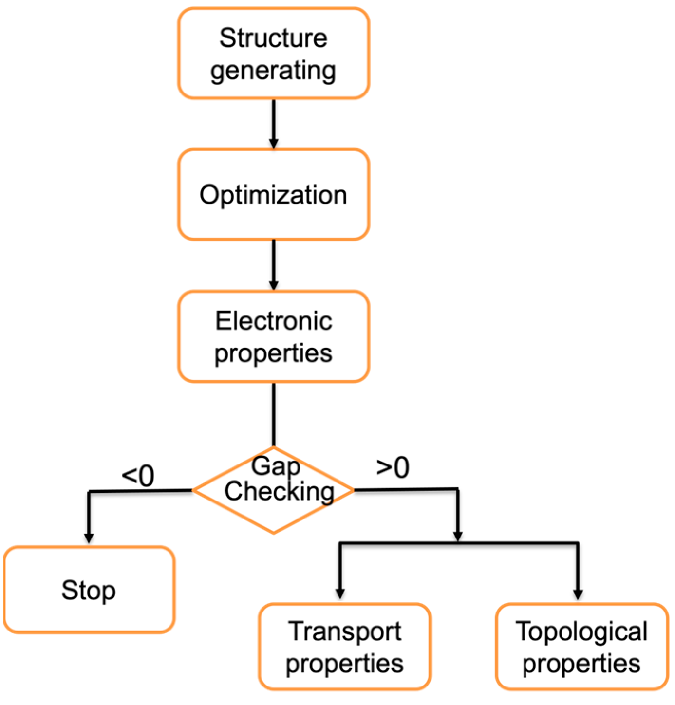
2. Computational Methods

The electronic structure calculations have been performed within the frame of the density functional theory using projector-augmented waves (PAW) [29] and planewaves techniques, as implemented in the VASP program [30,31,32]. The PBEsol [33] exchange-correlation functional has been used. As 4307 structures have been generated with a number of atoms in each unit cell varying from 5 to 63, full structural optimizations (atomic positions and cell parameters) have been performed along 3 steps from coarse level to accurate ones. For the coarse level, the kinetic energy cutoff has been set to the maximum value among the three atoms as recommended in the POTCAR file of VASP, i.e., 174.982 eV. For the more accurate levels, the kinetic energy cutoff was set to 300 eV and 400 eV. The energy and force thresholds employed for the structure optimizations have been set to 10−5 eV and 10−2 eV/Å, and the energy threshold for the subsequent electronic properties calculations has been set to 10−6 eV. The Brillouin zone (BZ) has been sampled with a k-point grid determined from the KSPACING parameter of VASP that is used to calculate the number of k-points from the formula
N i = max 1 ,   ceiling 2 π b i KSPACING ,
where bi is the lattice constant of the optimized structures. The values of KSPACING have been set to 0.8, 0.8, and 0.4 for each step. For the subsequent self-consistent (SCF) calculations, the k-spacing and planewave kinetic energy cutoff have been set to 0.1 and 450 eV. The electronic structure and charge density calculated from the SCF step have been used to analyze the topological properties within the quantum theory of atoms in molecules and crystals (QTAIMAC) [34], as implemented in Critic2 code [35]. The thermoelectric properties have been obtained from the semi-classical Boltzmann transport theory within the constant relaxation time approximation (CRTA) and the rigid band structure approximation as implemented in BoltzTraP2 code [36]. For the resolution of the Boltzmann transport equation, full BZ band structures are rebuilt for the k-points sampling and eigenvalues, for which a very dense k-point mesh is required, and the k-spacing has been set to 0.05.

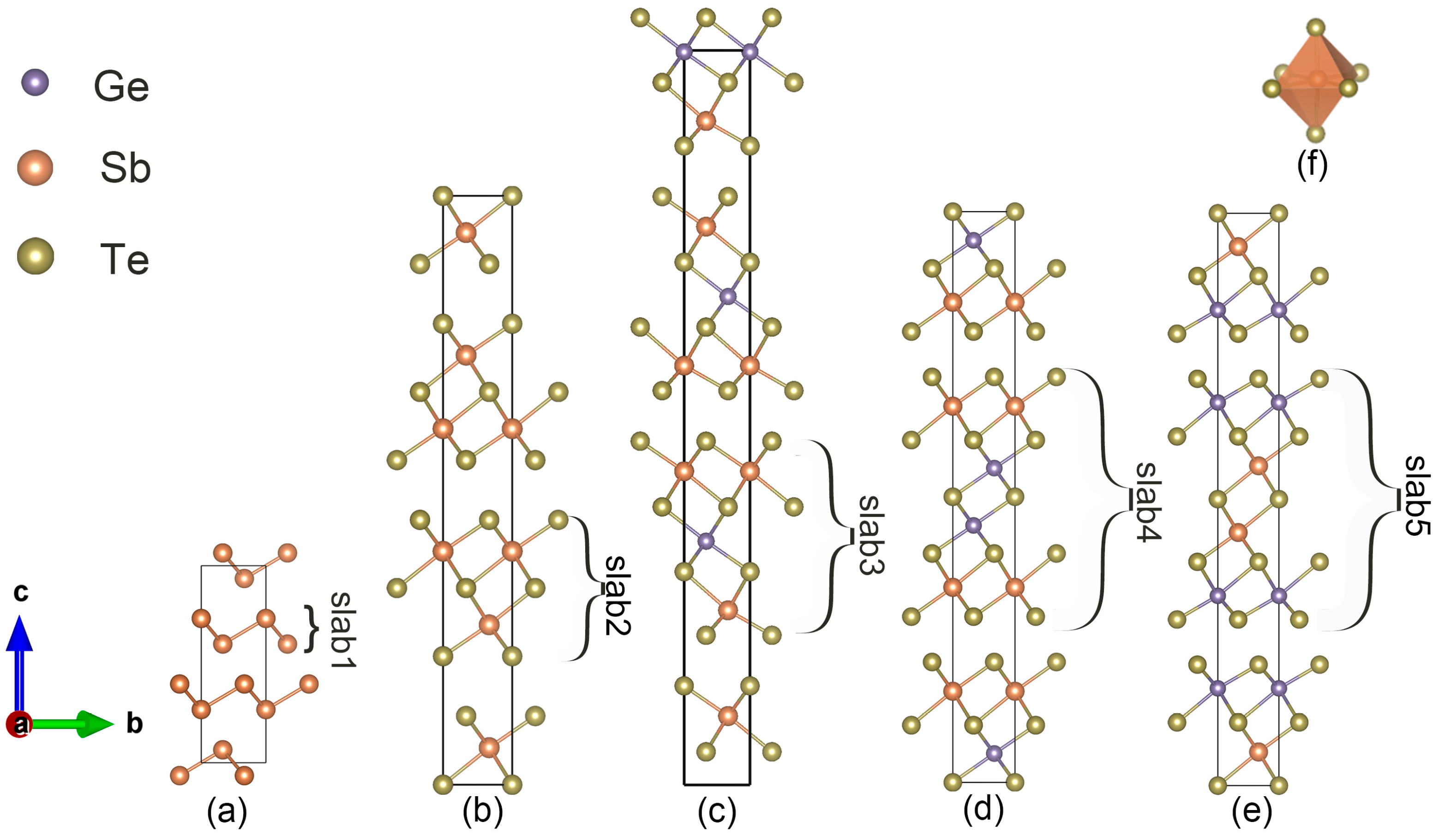
3. Structure Generation

The workflow of the high-throughput calculations performed in this work is illustrated in Figure 1. First, the structures are generated by the python script and fully optimized with VASP. The electronic properties are subsequently calculated, and the band gap energies are extracted. If the gap is found to be opened, the transport and topological properties are calculated; otherwise, the structure is discarded. At this point, one should underline that GGA functionals underestimate band gap energies; hence, compounds with an opened bandgap may be erroneously discarded from the list of candidates. This is, however, a weaker drawback than if the process had led to keeping metals in the list.
The slab candidates used to build the layered structures stem from naturally existing compounds from the n(GeTe)-m(Sb2Te3) system: Sb2Te3, GeSb2Te4, and Ge2Sb2Te5 with two stacking sequences. The atomic slabs are illustrated in Figure 2b–e. The bulk Sb has also been taken into account as it also possesses a layered structure (Figure 2a). The bulk Sb, Sb2Te3, and GeSb2Te4 crystallize in a rhombohedral lattice system (space group R 3 ¯ m) with 2, 5, and 7 atoms in the primitive cell stacked along the c-axis, and they can also be modeled in hexagonal unit cells. Inside the bulk Sb, Sb2Te3, and GeSb2Te4, three different atomic slabs with 2, 5, and 7 atomic layers are found, respectively. The bulk Ge2Sb2Te5 crystallizes in the P3m1 space group with two possible stacking sequences (stacking S1 and stacking S2, see Figure 2d,e), and consists of a nine-atomic-layer slab. The two sequences differ by the complete interchange of Sb and Te atoms in the layers. To provide a better illustration, a 1 × 1 × 2 supercell is depicted in Figure 2d,e. Hence, five atomic slabs consisting of 2, 5, 7, 9, and 9 atomic layers have been chosen as candidates to build the complex layered structures, the slabs being labeled as slab1, slab2, slab3, slab4, and slab5 in Figure 2. Each atom inside the slab is bonded with six adjacent atoms (Figure 2f), while the outermost Te atom in each slab is bonded with two atoms and presents a van der Waals interaction with the adjacent slab.
From the five slab candidates, many-layered structures can be built by combinations and perturbations. However, there are also many choices for the slab stacking sequences in the ab plane, which means that the coordinates of the outermost Te atoms from adjacent slabs should be constrained. To constrain the structures and maintain the space group of the complex structures, the coordinates in the ab plane have been constrained according to the following sequence: →(1/3, 2/3)→(2/3, 1/3)→(0,0)→. Three examples are shown in Figure 3 and the sequence of slabs with slab4—slab4—slab5—slab5, slab5—slab4—slab4—slab3—slab2, and slab3—slab1—slab3—slab4—slab5—slab2 in the unit cells are labeled as 4455, 54432, and 313452, respectively. Even though the atomic layers in a slab can also exist in many different possibilities, in this work, the slabs have been treated as a whole and the combinations have only been applied for the slab stacking sequences. The number of generated structures increases sharply with the increase in the number of slabs in the unit cells. Therefore, the maximum number of slabs has been set to seven. An amount of 4307 complex layered structures have been generated for the optimization step.
All the structures have been generated simply from geometric stacking, which cannot ensure the rationality of the structures. After generating the structures, we have optimized the so-generated structures from coarse to accurate levels by improving the kinetic cutoff and the k-mesh sampling of BZ. In the end, 1132 structures have been optimized with success.

4. Results

This section deals with the electron density topological analysis of the structures, the stability of the calculated structures, and their electronic and transport properties.

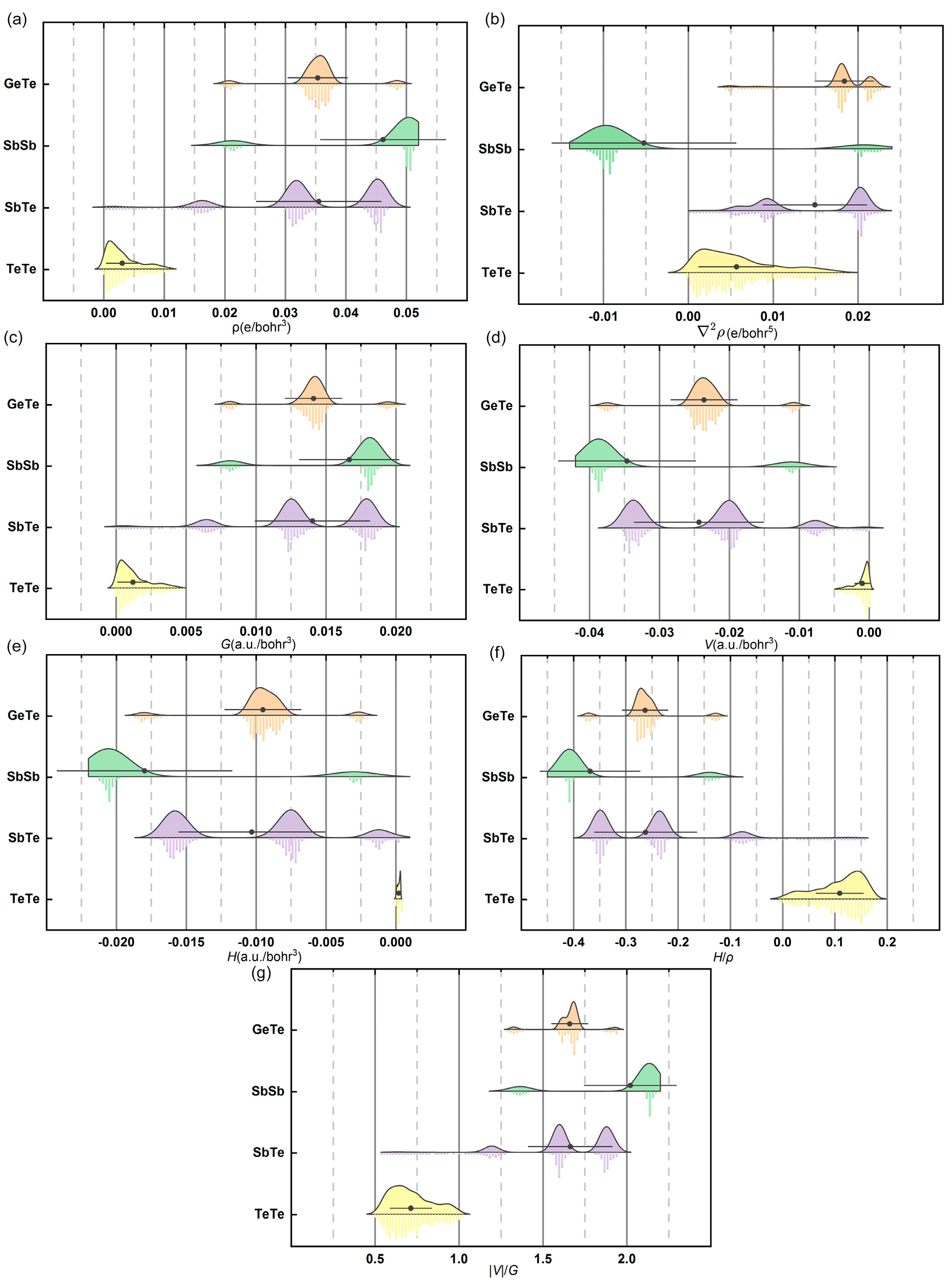
4.1. Electron Density Topology

Electron charge density values and distribution play an important role in the bonding trend characteristics and affect the thermoelectric properties. Therefore, the analysis of electron charge density and chemical bonding as developed by Bader and subsequent QTAIMAC methods can help us to explore the electronic character of the selected compounds. The key fields are the electron density ρ and its Laplacian ∇2ρ, from which the total energy density H, the kinetic energy density G, and potential one V can be derived. Besides, closed shell interactions (ionic, H-bonds, and van der Waals) have a large positive value of ∇2ρ over the entire interaction region, G/ρ > 1, |V|/G < 1, and a small ρ. Conversely, ∇2ρ < 0, G/ρ < 1, |V|/G > 2, and a large ρ are expected for shared interactions (covalent or polar bonds). Within the generated compounds, four types of bonds are found: Ge-Te, Sb-Sb, Sb-Te, and Te-Te. The corresponding QTAIMAC parameters are plotted in Figure 4. In agreement with the structure of the compounds, the QTAIMAC results evidence one type of bond for Ge-Te, Te-Te, and Sb-Sb and two types of bonds for Sb-Te: one corresponds to the bonds inside the slab and the other corresponds to a bond between slab1 and any other one. Small values of ρ and positive ∇2ρ with 1 < |V|/G < 2 have been evidenced at the BCPs of the Ge-Te and Sb-Te bonds. These characteristics agree with those defining the transit region according to Espinosa’s work [37]. In this region, bonds are neither pure covalent nor pure closed-shell interactions. The Te-Te bonds exhibit a positive bond degree (H/ρ) with |V|/G < 1 at their bond critical point. According to Espinoza’s bonding classification, these weak Te-Te bonds are associated with closed shell interactions and are expected to be of a van der Waals type. By contrast, most of the Sb-Sb bonds (those located in the slab) show a negative ∇2ρ, indicating an electron concentration at the bond critical point. The |V|/G ratio of the Sb-Sb bonds is also larger than two, suggesting that the Sb-Sb bonds involve covalent interactions.

4.2. Structure Stability

Stability is an essential property for any structure. In DFT, the current standard way to verify structure stability is to perform phonon calculations by means of DFPT. However, these calculations would require formidable computer resources for our many structures. Therefore, to investigate the relative stability of the layered structures, we start from the cohesive energy. Cohesive energy is the energy gained by arranging the atoms in a crystalline state, as compared with the gas state, and is given by the following:
E c o h Ge x Sb y Te z = E tot Ge x Sb y Te z x E atom Ge y E atom Sb z E atom Te x + y + z
where E tot Ge x Sb y Te z is the total energy and E tot is the energy of the isolated atoms. Cohesive energy can provide information on the relative stability of the compounds of interest. Indeed, insulators and semiconductors, which have large cohesive energies, are strongly bonded and have good stability [38]. The calculated cohesive energy is shown in Figure 5. The value of the cohesive energies is projected on the left and right planes. The composition of the generated structures is projected to the bottom plane and shown by the ternary diagram. As discussed above, the layered structures are based on only five slabs: Sb, Sb2Te3, GeSb2Te4, Ge2Sb2Te5-S1, and Ge2Sb2Te5-S2; hence, the compositional range of each element is 22.2–100% for Sb, 0–22.2% for Ge, and 0–60% for Te. The projection of composition only occupies part of the ternary diagram. As shown in Figure 5, the range of the cohesive energy varies from −2.585 eV/at. to −2.922 eV/at.
As shown in the projection on the right plane (Figure 5), the value of cohesive energy decreases with the increase in the Ge content. According to the previous electron density topological analysis, all the bonding interactions inside the slabs are located at the transit region with neither pure covalent nor pure ionic interactions. Comparing the pure elements Sb, Ge, and Te, Ge exhibits stronger interactions, which is consistent with the calculated cohesive energy of −4.16 eV/at., −2.87 eV/at., and −3.12 eV/at. for Ge, Te, and Sb, respectively. As for Sb and Te, they have a similar impact on the cohesive energy.
Enthalpies of formation correspond to the difference between the total energy of a target compound AxBy and that of its constitutive elements A, B, and so on, taken in their standard reference state. The formation energy of a complex structure of GexSbyTez is calculated according to Equation (3):
E f Ge x Sb y Te z = E tot Ge x Sb y Te z x μ Ge y μ Sb z μ Te x + y + z
where μ is the chemical potential of the pure elements. For most cases, chemical potentials are equal to the DFT total energies of their ground states.
Stevanović et al. [39] pointed out that when all the compounds and elements of interest pertain to similar classes of materials (e.g., metals, semiconductors), the calculation of the studied systems can be performed within one of the standard approximations of DFT, namely, the LDA or GGA, which benefit from the cancellation of errors associated with the similarly imperfect description of bonding in AxBy and its constitutive solid elements A and B. In our case, Ge, Sb, and Te elements are semiconductors located in the p block of the periodic table. All the generated structures are oxygen atom-free, which suppresses the problem of the inadequate calculation of the ground state of this atom by DFT at 0K. The calculated formation energies are shown in Figure 6. All formation energies present negative values varying from −0.53 eV/at. to −0.27 eV/at. Combining the projections on the right and left planes, we can observe that the formation enthalpy increases with the increase in Sb content. Based on the configuration of the structural generation, all layered structures are built from different slabs maintained together by van der Waals forces. Two new Sb-Te bonds are created when inserting slab1 (Sb-Sb) between two slabs terminated with Te (slabs two to five), which strengthen the new structures. Table 1 shows the calculated formation and cohesive energies of six selected structures that have been chosen based on their narrow band gap and high power factor (see electronic and transport properties sections).

4.3. Electronic Properties

Based on the optimized structures, the electronic band structures have been calculated with the PBEsol functional. Although the spin-orbit coupling (SOC) may have a sizable effect on the band structure for compounds with heavy elements, the calculations have been performed without SOC. Indeed, for our complex structures, SOC would have consumed too many calculation resources. The results are presented in Figure 7. The negative values are a consequence of the valence and conduction band overlapping and reflect the metallic character of the compound. As can be seen, the band gap varies from −0.535 to 0.655 eV. The distribution of band gap energies can be divided into three parts: the wide-gap region (gap > 0.25 eV), the semi-conductor/metal region (0 eV < gap < 0.25 eV), and the metallic region (gap < 0 eV).
An amount of 43 layered compounds are located in the wide-gap region. They are reported in Table 2 with their band gap value and gap type. Among these compounds, none of them contain slab1 and slab5. The compounds generated from only one type of slab (4, 333, and 222) belong to this region. The gap is decreasing from 4 to 333 and to 222. The decreasing band gap from the highest value is obtained starting from compound four. Generally, the compounds with high band gap values are located at the low-Sb part. The slab5 can seriously decrease the band gap for the models. Following the band theory, the Seebeck coefficient can be given as the following:
S = k B 2 e 1 n μ n + p μ p 2 E f k B T n μ n 2 E f + E g k B T p μ p
where kB is the Boltzmann constant, e is the elementary charge, Ef and Eg are the Fermi level and the band gap energy, μn and μp are the mobility of electrons and holes, and n and p are the number of electrons and holes, respectively. There is a positive relationship between the Seebeck coefficient and band gap values. However, the electrical conductivity decreases sharply with the increase in the band gap and deteriorates the power factor (PF = S2σ).
An amount of 358 layered compounds belong to the semi-conductor/metal region, among which, the more they are metallic, the more slab1 and slab5 are represented. The metallic character of Ge2Sb2Te5-S2, from which slab5 is extracted, has been assessed (see Ref. [10]). The compounds in the semi-conductor/metal region are expected to present promising TE properties with moderate Seebeck coefficients and electrical conductivity. The remaining 731 layered compounds have been evidenced to be metallic ones.
For the following, we have chosen six compounds located in the wide-gap and semi-conductor/metal region and calculated their electronic structures. The band structures computed with the PBEsol functional are shown in Figure 8 and the corresponding DOS is illustrated in Figure 9. The band structures range from −2 eV to 2 eV. The space group numbers of the generated compounds are 156, 164, or 166. To keep the k-path consistent, the conventional unit-cells (Figure 10b) are used to calculate the band structures for the compound with space group 166 (Figure 10a). The shapes of the Brillouin zone of their primitive and conventional cells are represented, as well as the path between high symmetry points chosen for the band structure calculations, which is Γ-K-M-Γ-A-H-L-A. Due to the excessive delocalization of the occupied states by the GGA functional, a serious underestimation of the band gap is usually observed, which is a common problem in GGA functionals. However, since there are too many compounds to investigate, we only have used the PBEsol functional to calculate the transport properties.
The layered compound 31 exhibits characteristics of an indirect band gap semiconductor with an energy band gap of 0.006 eV, with CBM located on the A-H line, and VBM located on the Γ-K line. There are four second-highest VBMs and four second-lowest CBMs within an energy range of 0.1 eV relative to VBMs and CBMs, respectively. However, the band near the Fermi level is very soft, and the slope of the DOS is moderate in both the valence and conduction parts.
Sb2Te3 (222) belongs to the rhombohedral system with a space group R 3 ¯ m. When the structure is converted to the space group P3m1, the conventional cell contains three five-atom-layer slabs. After optimization, the lattice constants are a,b = 4.32 Å and c = 31.94 Å. As shown in Figure 8b, Sb2Te3 is a multi-valley semiconductor with a direct band gap of 0.292 eV. Both the CBM and the VBM are situated at the Γ point (0, 0, 0). Within the conduction bands, three second-highest minima can be found, two of them along the Γ-M line located at (0.058, 0.058, 0) and (0.153, 0.153, 0) and one along the L-A line located at (0.104, 0.104, 0.500). Multi-valley band structures can boost the TE properties: a multi-gap between the valley providing several electron transition pathways, and a band alignment boosting the Seebeck coefficient. From the density of states shown in Figure 9, we observe that the slope of the total DOS near the VBM is much more cliffy than that of the CBM, indicating a higher Seebeck coefficient for p-type doping. The DOS of 222 has a strong Te-p state character near the Fermi level, while the conduction band orbitals near the CBM are equally contributed by the hybridization between Te-p and Sb-p states.
In the case of 333 (Figure 8c and Figure 9c), the band structure evidences the features of a semiconductor with a direct band gap. The lowest energy value of the conduction band and the highest one of the valence band are both located at point A, and the band gap energy value is 0.553 eV. Moreover, at the bottom of the conduction band, there are multiple valleys with similar energy minima, resulting in high degeneracy. Therefore, the Seebeck coefficient of the n-type doped compound should theoretically be better than those of the p-type doped one. The valence and conduction bands are mainly contributed by Te-p and Te-p+Sb-p+Ge-p orbitals, respectively.
The band gap of 4455 (Figure 8d and Figure 9d) is an indirect one, with the lowest energy value of the conduction band at point A and the highest energy value of the valence band between L and A. The energy gap value is 0.011 eV. Near Γ, the valence band is very flat and has small parabolic characteristics (Te-p type orbitals); hence, holes should have a large effective mass resulting in a high Seebeck coefficient for p-type doped 4455.
For 54432 (Figure 8e and Figure 9e), the CBM is located at the Γ point, the VBM is located between L and A, and the energy band gap is 0.021 eV. Notably, near the top of the valence band, several states bear a similar energy, resulting in converging energy bands. So, the p-type doped compound may have a higher Seebeck coefficient than the n-type doped one. However, near Γ, the conduction band is very flat; hence, electrons should have a large effective mass resulting in a larger Seebeck coefficient for the n-type doped 54432 than for the p-type one. As we can see, these two effects on the Seebeck coefficient contradict each other, so it is difficult to conclude about the thermopower on the basis of the description of the band structure only.
For 313452, the lowest energy values of the conduction band are all located between Γ and M, the highest energy values of the valence band are all located between A and H, and the band gap energy value is 0.003 eV. The valence band is contributed by a combination of the p orbitals of Te, Sb, and Ge.
It can be seen from the density of states diagrams that the DOS is zero in a small range near the Fermi level. In the valence band or conduction band, the density of states increases, and it has a steep peak near the Fermi level, especially in 4455 and 54432, and to a lesser extent in 313452. This behavior should result in a large Seebeck coefficient, which is beneficial to achieving a high power factor.

4.4. Transport Properties

The electronic conductivity (σ) and the electronic thermal conductivity (κe) calculated by BolzTrap2 are given as the ratios σ/τ and κe/τ, respectively. The relaxation time τ depends on the charge carrier concentration, the temperature, and the electron energy, which can be evaluated from deformation potential (DP) theory. However, due to the high computational burden of DP calculations, we keep τ undetermined in the following. The best TE properties are obtained for chalcogenides with carrier concentrations around 1019 carriers/cm3, so the doping dependence has been investigated in the domain of carrier concentrations ranging from 1017 cm−3 to 1022 cm−3. The calculations have been performed for both electron-doping and hole-doping. The temperature and doping dependence of transport properties S, σ/τ, and PF (S2σ) are shown in Figure 11, Figure 12 and Figure 13 for all the layered compounds having a GGA band gap higher than 0. eV (around 401 compounds). In these figures, the diameter and the color of the balls are representative of the magnitude of the power factor. The graphs show an uneven spreading of points along the x-axis. Along the y-axis, opposite signs of the Seebeck coefficient can be found on the two halves of the graph with respect to the zero due to the two types of doping. The color gradient shows a steady increase in PF toward maximization when either the Seebeck coefficient or the electrical conductivity increases.
By contrast to what is observed for intermediate and high doping levels (Figure 12 and Figure 13), a more pronounced asymmetrical distribution of the Seebeck coefficient values between the positive and negative ones is observed at low doping levels (Figure 11). This could be related to an insufficient doping level to compensate for the pristine carrier concentration. With the increase in temperature, the electrical conductivity increases, while the Seebeck coefficient decreases. It is difficult to reach both high Seebeck and high conductivity at the same time, as shown by the absence of points in that region. The highest Seebeck coefficients can be reached at moderate temperatures and low doping levels. The distribution of points according to their color suggests that the Seebeck coefficient has stronger effects on the PF than the electrical conductivity, as the points with the same color parallel the x-axis.
At low doping levels, irrespective of the temperature, (see Figure 11a), the n-type compounds present a higher power factor than the p-type ones. Nonetheless, with the increasing temperature, more p-type compounds show high PF.
At moderate- and high-carrier doping levels (Figure 12 and Figure 13), irrespective of the charge carrier types, the Seebeck coefficient values spread over a slightly larger range as the temperature increases, and the compounds bearing a low Seebeck coefficient value (around zero) tend to migrate toward the extremes of the domain. The largest number of compounds bearing high PF values has been found for the intermediate doping level.
The maximum PF/τ is found in the layered compound 3541153, which is 2.79 × 10¹² Wm−1K−2s−1 for an electron doping level of 3.16 × 1021 cm−3 and at 850 K. Two p-type and 86 n-type layered compounds have been identified as promising candidates (PF/τ > 1012 Wm−1K−2s−1) for TE applications.

5. Conclusions

In this work, 4307 layered structures have been generated by a high-throughput computer program, among which 1132 structures have been successfully optimized to their ground states. Electronic properties, transport properties, and topological properties have been investigated. All Ge-Te and Sb-Te bonds are located at the transit region with small values of electron density ρ and positive Laplacian ∇2ρ with 1 < |V|/G < 2, while Te-Te BCPs exhibit a positive bond degree (H/ρ) with |V|/G < 1. The maximum PF/τ is found in the layered compound 3541153, which is 2.79 × 10¹² Wm−1K−2s−1 for an electron doping level of 3.16 × 1021 cm−3 and at 850 K. Two p-type and 86 n-type layered compounds have been identified as promising candidates for TE applications.

Author Contributions

Conceptualization, P.B. and M.-C.R.; methodology, J.T., W.M., P.B., M.C. and M.-C.R.; software, J.T. and W.M.; validation, P.B., M.C. and M.-C.R.; formal analysis, J.T. and W.M.; investigation, J.T. and W.M.; resources, P.B. and M.-C.R.; data curation, J.T. and W.M.; writing—original draft preparation, J.T. and W.M.; writing—review and editing, P.B., M.C. and M.-C.R.; visualization, J.T. and W.M.; supervision, P.B. and M.-C.R.; project administration, P.B. and M.-C.R. All authors have read and agreed to the published version of the manuscript.

Funding

This research received no external funding.

Data Availability Statement

The original data presented in the study are openly available in Zenodo, http://doi.org/10.5281/zenodo.10994229.

Acknowledgments

The authors are thankful to the China Scholarship Council for financing the PhD thesis of J. Tian. This work was granted access to the HPC resources A0130806881 made by the “Grand Equipement National de Calcul Intensif (GENCI)”. The “Centre de Calcul Intensif d’Aix-Marseille” is acknowledged for granting access to its high-performance computing resources as well as the “Centre Régional de Compétences en Modélisation Moléculaire” of the Chemistry Federation of the Aix-Marseille University.

Conflicts of Interest

The authors declare no conflicts of interest.

References

  1. Luo, Y.; Yang, J.; Jiang, Q.; Li, W.; Zhang, D.; Zhou, Z.; Cheng, Y.; Ren, Y.; He, X. Progressive Regulation of Electrical and Thermal Transport Properties to High-Performance CuInTe2 Thermoelectric Materials. Adv. Energy Mater. 2016, 6, 1600007. [Google Scholar] [CrossRef]
  2. Kumar, A.; Chaturvedi, K.M.; Bano, S.; Govind, B.; Misra, D.K. Enhanced thermoelectric performance of p-type ZrCoSb0.9Sn0.1 via Tellurium doping. Mater. Chem. Phys. 2021, 258, 123915. [Google Scholar] [CrossRef]
  3. Rausch, E.; Balke, B.; Deschauer, T.; Ouardi, S.; Felser, C. Charge carrier concentration optimization of thermoelectric p-type half-Heusler compounds. APL Mater. 2015, 3, 41516. [Google Scholar] [CrossRef]
  4. Wei, Z.; Li, Z.; Luo, P.; Zhang, J.; Luo, J. Simultaneously increased carrier concentration and mobility in p-type Bi0.5Sb1.5Te3 throng Cd doping. J. Alloy. Compd. 2020, 830, 154625. [Google Scholar] [CrossRef]
  5. Kumar, A.; Bano, S.; Govind, B.; Bhardwaj, A.; Singh, V.N. Enhanced thermoelectric performance of n-type Zr0.66Hf0.34Ni1+xSn Heusler nanocomposites. J. Alloy. Compd. 2022, 900, 163454. [Google Scholar] [CrossRef]
  6. Yu, B.; Zebarjadi, M.; Wang, H.; Lukas, K.; Wang, H.; Wang, D.; Opeil, C.; Dresselhaus, M.; Chen, G.; Ren, Z. Enhancement of Thermoelectric Properties by Modulation-Doping in Silicon Germanium Alloy Nanocomposites. Nano Lett. 2012, 12, 2077–2082. [Google Scholar] [CrossRef] [PubMed]
  7. Tang, X.; Zhang, B.; Zhang, X.; Wang, S.; Lu, X.; Han, G.; Wang, G.; Zhou, X. Enhancing the Thermoelectric Performance of p-Type Mg3Sb2 via Codoping of Li and Cd. ACS Appl. Mater. Interfaces 2020, 12, 8359–8365. [Google Scholar] [CrossRef] [PubMed]
  8. Pei, Y.; Shi, X.; LaLonde, A.; Wang, H.; Chen, L.; Snyder, G.J. Convergence of electronic bands for high performance bulk thermoelectrics. Nature 2011, 473, 66–69. [Google Scholar] [CrossRef]
  9. Balout, H.; Boulet, P.; Record, M.-C. Strain-induced electronic band convergence: Effect on the Seebeck coefficient of Mg2Si for thermoelectric applications. J. Mol. Model. 2017, 23, 130. [Google Scholar] [CrossRef]
  10. Tian, J.; Ma, W.; Record, M.-C.; Boulet, P. High Thermoelectric Performance of Ge-Sb-Te Nanosheets: A Density Functional Study. J. Electron. Mater. 2024. Submitted. [Google Scholar]
  11. Yu, J.; Fu, C.; Liu, Y.; Xia, K.; Aydemir, U.; Chasapis, T.C.; Snyder, G.J.; Zhao, X.; Zhu, T. Unique role of refractory Ta alloying in enhancing the figure of merit of NbFeSb thermoelectric materials. Adv. Energy Mater. 2018, 8, 1701313. [Google Scholar] [CrossRef]
  12. Fu, T.; Xin, J.; Zhu, T.; Shen, J.; Fang, T.; Zhao, X. Approaching the minimum lattice thermal conductivity of p-type SnTe thermoelectric materials by Sb and Mg alloying. Sci. Bull. 2019, 14, 1024–1030. [Google Scholar] [CrossRef] [PubMed]
  13. Wang, S.; Sun, Y.; Yang, J.; Duan, B.; Wu, L.; Zhang, W.; Yang, J. High Thermoelectric Performance in Te-free (Bi,Sb)2Se3 via Structural Transition Induced Band Convergence and Chemical Bond Softening. Energy Environ. Sci. 2016, 9, 3436–3447. [Google Scholar] [CrossRef]
  14. Ying, P.; Li, X.; Wang, Y.; Yang, J.; Fu, C.; Zhang, W.; Zhao, X.; Zhu, T. Hierarchical Chemical Bonds Contributing to the Intrinsically Low Thermal Conductivity in α-MgAgSb Thermoelectric Materials. Adv. Funct. Mater. 2017, 27, 1604145. [Google Scholar] [CrossRef]
  15. Li, W.; Lin, S.; Ge, B.; Yang, J.; Zhang, W.; Pei, Y. Low Sound Velocity Contributing to the High Thermoelectric Performance of Ag8SnSe6. Adv. Sci. 2016, 3, 1600196. [Google Scholar] [CrossRef] [PubMed]
  16. Charoenphakdee, A.; Kurosaki, K.; Muta, H.; Uno, M.; Yamanaka, S. Ag8SiTe6: A New Thermoelectric Material with Low Thermal Conductivity. Jpn. J. Appl. Phys. 2009, 48, 011603. [Google Scholar] [CrossRef]
  17. Zhu, T.J.; Zhang, S.N.; Yang, S.H.; Zhao, X.B. Improved Thermoelectric Figure of Merit of Self-Doped Ag8−xGeTe6 Compounds with Glass-like Thermal Conductivity. Phys. Status Solidi RRL 2010, 4, 317–319. [Google Scholar] [CrossRef]
  18. Zhao, L.-D.; Lo, S.-H.; Zhang, Y.; Sun, H.; Tan, G.; Uher, C.; Wolverton, C.; Dravid, V.P.; Kanatzidis, M.G. Ultralow Thermal Conductivity and High Thermoelectric Figure of Merit in SnSe Crystals. Nature 2014, 508, 373–377. [Google Scholar] [CrossRef]
  19. Curtarolo, S.; Hart, G.L.W.; Nardelli, M.B.; Mingo, N.; Sanvito, S.; Levy, O. The High-Throughput Highway to Computational Materials Design. Nat. Mater. 2013, 12, 191–201. [Google Scholar] [CrossRef] [PubMed]
  20. Fan, T.; Oganov, A.R. Discovery of High Performance Thermoelectric Chalcogenides through First-Principles High-Throughput Screening. J. Mater. Chem. C 2021, 9, 13226–13235. [Google Scholar] [CrossRef]
  21. Xu, G.; Xin, J.; Deng, H.; Shi, R.; Zhang, G.; Zou, P. High-Throughput Screening of High- Performance Thermoelectric Materials with Gibbs Free Energy and Electronegativity. Materials 2023, 16, 5399. [Google Scholar] [CrossRef] [PubMed]
  22. Wang, S.; Wang, Z.; Setyawan, W.; Mingo, N.; Curtarolo, S. Assessing the Thermoelectric Properties of Sintered Compounds via High-Throughput Ab-Initio Calculations. Phys. Rev. X 2011, 1, 021012. [Google Scholar]
  23. Yang, J.; Li, H.; Wu, T.; Zhang, W.; Chen, L.; Yang, J. Evaluation of Half-Heusler Compounds as Thermoelectric Materials Based on the Calculated Electrical Transport Properties. Adv. Funct. Mater. 2008, 18, 2880–2888. [Google Scholar] [CrossRef]
  24. Carrete, J.; Mingo, N.; Wang, S.; Curtarolo, S. Nanograined Half-Heusler Semiconductors as Advanced Thermoelectrics: An Ab Initio High-Throughput Statistical Study. Adv. Funct. Mater. 2014, 24, 7427–7432. [Google Scholar] [CrossRef]
  25. Gan, Y.; Wang, G.; Zhou, J.; Sun, Z.; Qiu, D.; Singh, D.J.; Xi, J.; Yang, J.; Xi, L. Prediction of Thermoelectric Performance for Layered IV-V-VI Semiconductors by High-Throughput Ab Initio Calculations and Machine Learning. npj Comput. Mater. 2021, 7, 176. [Google Scholar] [CrossRef]
  26. Jin, Y.; Wang, X.; Yao, M. High-Throughput Deformation Potential and Electrical Transport Calculations. npj Comput. Mater. 2023, 9, 190. [Google Scholar] [CrossRef]
  27. Kanatzidis, M.G. The Role of Solid-State Chemistry in the Discovery of New Thermoelectric Materials. Semicond. Semimet. 2001, 69, 51–100. [Google Scholar]
  28. Harker, D. The Crystal Structure of the Mineral Tetradymite, Bi2Te2S. Z. Für Krist.-Cryst. Mater. 1934, 89, 175–181. [Google Scholar] [CrossRef]
  29. Kresse, G.; Joubert, D. From Ultrasoft Pseudopotentials to the Projector Augmented-Wave Method. Phys. Rev. B 1999, 59, 1758–1775. [Google Scholar] [CrossRef]
  30. Kresse, G.; Furthmüller, J. Efficient Iterative Schemes for Ab Initio Total-Energy Calculations Using a Plane-Wave Basis Set. Phys. Rev. B 1996, 54, 11169–11186. [Google Scholar] [CrossRef]
  31. Kresse, G.; Furthmüller, J. Efficiency of Ab-Initio Total Energy Calculations for Metals and Semiconductors Using a Plane-Wave Basis Set. Comput. Mater. Sci. 1996, 6, 15–50. [Google Scholar] [CrossRef]
  32. Kresse, G.; Hafner, J. Ab Initio Molecular Dynamics for Liquid Metals. Phys. Rev. B 1993, 47, 558–561. [Google Scholar] [CrossRef] [PubMed]
  33. Perdew, J.P.; Ruzsinszky, A.; Csonka, G.I.; Vydrov, O.A.; Scuseria, G.E.; Constantin, L.A.; Zhou, X.; Burke, K. Restoring the Density-Gradient Expansion for Exchange in Solids and Surfaces. Phys. Rev. Lett. 2008, 100, 136406. [Google Scholar] [CrossRef] [PubMed]
  34. Bader, R.F.W.; Beddall, P.M.; Cade, P.E. Partitioning and Characterization of Molecular Charge Distributions. J. Am. Chem. Soc. 1971, 93, 3095–3107. [Google Scholar] [CrossRef]
  35. Otero-de-la-Roza, A.; Blanco, M.A.; Pendaás, A.M.; Luaña, V. Critic: A New Program for the Topological Analysis of Solid-State Electron Densities. Comput. Phys. Commun. 2009, 180, 157–166. [Google Scholar] [CrossRef]
  36. Madsen, G.K.H.; Carrete, J.; Verstraete, M.J. BoltzTraP2, a Program for Interpolating Band Structures and Calculating Semi-Classical Transport Coefficients. Comput. Phys. Commun. 2018, 231, 140–145. [Google Scholar] [CrossRef]
  37. Espinosa, E.; Alkorta, I.; Elguero, J.; Molins, E. From Weak to Strong Interactions: A Comprehensive Analysis of the Topological and Energetic Properties of the Electron Density Distribution Involving X–H⋯F–Y Systems. J. Chem. Phys. 2002, 117, 5529–5542. [Google Scholar] [CrossRef]
  38. Harrison, W.A. Coulomb Interactions in Semiconductors and Insulators. Phys. Rev. B 1985, 31, 2121–2132. [Google Scholar] [CrossRef]
  39. Stevanović, V.; Lany, S.; Zhang, X.; Zunger, A. Correcting Density Functional Theory for Accurate Predictions of Compound Enthalpies of Formation: Fitted Elemental-Phase Reference Energies. Phys. Rev. B 2012, 85, 115104. [Google Scholar] [CrossRef]
Figure 1. Workflow of the high-throughput calculations.
Crystals 14 00403 g001
Figure 2. Slab candidates for the structure generation taken from the: (a) Sb, (b) Sb2Te3, (c) GeSb2Te4, (d) Ge2Sb2Te5-S1 and (e) Ge2Sb2Te5-S2 structures. The polyhedron (f) shows the atomic environment for the atoms inside the slab.
Crystals 14 00403 g002
Figure 3. Structure of the 4455, 54422, and 313452 stacking sequences.
Crystals 14 00403 g003
Figure 4. Raincloud plots of the electron density (a) and its Laplacian (b), kinetic energy density (c), potential energy density (d), total energy density (e), bond degree (f), and dimensionless |V|/G ratio (g). The points indicate the average value of the distribution, and the horizontal line corresponds to the standard deviation.
Crystals 14 00403 g004
Figure 5. Cohesive energy of the studied systems. The cohesive energy is projected on the left (orange color) and right (green color) planes. The projection on the bottom plane (black color) gives the composition of the compounds.
Crystals 14 00403 g005
Figure 6. Formation energy of the studied systems. The formation energy is projected on the left (orange color) and right (green color) planes. The projection on the bottom plane (black plane) gives the composition of the compounds.
Crystals 14 00403 g006
Figure 7. Distribution of band gap values with the corresponding projections on left (orange color), right (green color) and bottom (black color) planes.
Crystals 14 00403 g007
Figure 8. Calculated electronic band structures of layered compounds 31 (a), 222 (b), 333 (c), 4455 (d), 54432 (e), and 313452 (f), calculated with the PBEsol functional. The red dashed lines correspond to the Fermi energy.
Crystals 14 00403 g008
Figure 9. Total and projected DOS of layered compounds 31 (a), 222 (b), 333 (c), 4455 (d), 54432 (e), and 313452 (f) calculated with the PBEsol functional. The energies are shifted using the Fermi energy.
Crystals 14 00403 g009
Figure 10. Brillouin zone of the primitive cell of Sb2Te3 (group number 166) (a) and conventional cell of Sb2Te3 (after transformation into group number 164) (b). The k-point path along Γ-K-M-Γ-A-H-L-A used in the band structure calculations is drawn in green.
Crystals 14 00403 g010
Figure 11. Seebeck coefficient versus electron conductivity (divided by τ). The colors represent the magnitude of the power factor (S2σ). The reported values are averaged over the three directions for T = 300 K (a), 500 K (b), 700 K (c), and 900 K (d), and doping levels of 1018 cm−3 for both n-type and p-type. Only materials with band gap higher than 0 eV are considered.
Crystals 14 00403 g011
Figure 12. Seebeck coefficient versus electron conductivity (divided by τ). The colors represent the magnitude of the power factor (S2σ). The reported values are averaged over the three directions for T = 300 K (a), 500 K (b), 700 K (c), and 900 K (d), and doping levels of 1020 cm−3 for both n-type and p-type. Only materials with band gap higher than 0 eV are considered.
Crystals 14 00403 g012
Figure 13. Seebeck coefficient versus electron conductivity (divided by τ). The colors represent the magnitude of the power factor (S2σ). The reported values are averaged over the three directions for T = 300 K (a), 500 K (b), 700 K (c), and 900 K (d), and doping levels of 1022 cm−3 for both n-type and p-type. Only materials with band gap higher than 0 eV are considered.
Crystals 14 00403 g013
Table 1. Lattice parameters (in Å) and formation and cohesive energies (in eV/atom) of selected structures.
Compounds31222333445554432313452
a4.344.324.304.284.294.30
c17.4031.9442.8475.2781.4781.94
Formation energy−0.32−0.27−0.28−0.31−0.30−0.30
Cohesive energy−2.80−2.70−2.84−2.91−2.87−2.84
Table 2. Band gap values and types of compounds in the wide band gap region.
CompoundsCBM-VBM (eV)CBM-VBM TypeCompoundsCBM-VBM (eV)CBM-VBM Type
40.6553Indirect320.4727Direct
343340.6457Indirect342320.4548Direct
433340.6424Indirect4322340.4441Direct
34330.6242Indirect233420.4372Direct
24340.5899Indirect422420.4364Indirect
444230.5899Indirect234320.4246Indirect
34434430.5833Indirect2322330.4243Direct
3420.5755Indirect4224240.4235Indirect
4320.5749Indirect32230.4166Direct
3334320.5748Direct42220.3872Direct
442430.5747Indirect2332230.3855Direct
4242330.5707Indirect2422320.3752Direct
44230.5574Indirect2242320.3732Direct
3334230.5566Indirect4222320.3717Direct
3330.5526Indirect2224320.3411Direct
4342320.5429Indirect222440.3406Direct
323240.5359Direct222320.3199Direct
242330.5294Indirect3332220.3156Direct
332330.5251Direct23232220.2964Direct
4333230.5083Direct2220.2922Direct
24424420.4940Direct3422220.2882Indirect
43323340.4841Direct
Disclaimer/Publisher’s Note: The statements, opinions and data contained in all publications are solely those of the individual author(s) and contributor(s) and not of MDPI and/or the editor(s). MDPI and/or the editor(s) disclaim responsibility for any injury to people or property resulting from any ideas, methods, instructions or products referred to in the content.

