
Effects of Al and N2 Flow Sequences on the Interface Formation of AlN on Sapphire by EVPE

Department of Electronic Science and Engineering, Kyoto University, Kyoto 615-8510, Japan
*
Author to whom correspondence should be addressed.
Crystals 2017, 7(5), 123; https://doi.org/10.3390/cryst7050123
Submission received: 15 March 2017
/
Revised: 18 April 2017
/
Accepted: 21 April 2017
/
Published: 27 April 2017
(This article belongs to the Special Issue Advances in GaN Crystals and Their Applications)
Abstract
:The interface formation mechanisms of AlN films on sapphire substrates grown by the elementary source vapor phase epitaxy (EVPE) method, which is a new AlN bulk fabrication method using Al and N2 as precursors, are investigated. Supplying N2 after the substrate temperature reaches the growth temperature [Process N2(GT)] causes the interface to become rough due to the thermal decomposition of sapphire. Self-separation occasionally occurs with the Process N2(GT), suggesting that the rough interface generates self-separating films with little strain. On the other hand, supplying N2 beginning at room temperature forms a relatively smooth interface with voids, which can be realized by the reaction between a nitrided sapphire surface and an Al source.
1. Introduction
AlN bulk crystals are promising as substrates of AlGaN-based deep ultraviolet light emitters and high-frequency electronic devices with high-breakdown voltages. Currently, AlN substrates are fabricated mainly by the physical vapor transport method [1,2,3,4,5] and hydride vapor phase epitaxy method [6,7,8,9,10]. To lower costs, increase the diameter, and improve the crystalline qualities, these methods must be refined. To this end, we have proposed a new growth method of AlN substrates: elementary source vapor phase epitaxy (EVPE) [11,12]. EVPE uses low cost and ecological precursors (Al metal and N2), and a (0001) sapphire substrate as a seed crystal for large-area growth. EVPE can fabricate AlN with a maximum growth rate of 18 µm/h and a minimum dislocation density of 5 × 108 cm−2 [11,12].
Thick AlN growth on sapphire substrates usually causes epilayer cracking due to the thermal expansion mismatch between AlN and sapphire, especially for high temperature growth [10,13]. Therefore, a method to relax the thermal stress is required. EVPE has enabled the growth of crack-free films even with a thickness of 18 µm because the voids generated at the AlN/sapphire interface during the EVPE growth may reduce the strain [11,12]. In addition, EVPE can induce spontaneous separation of AlN films from the sapphire substrates. A study on the void formation and self-separation mechanisms should realize growth of freestanding AlN substrates with less strain. In this study, the strain in AlN films on sapphire and self-separated AlN from sapphire are evaluated. In addition, the interface formation mechanisms are investigated with an emphasis on the Al and N2 gas flow sequences.
2. Experiments
Details of the growth apparatus are described in the literature [11,12]. A laboratory-built, horizontal, hot-wall reactor with induction heating systems was used in AlN EVPE and the annealing treatment of sapphire. The reactor has two heating zones: a source zone upstream of the reactor and a growth zone downstream. The temperature of each heating zone can independently be controlled. Al and N2 were used as source gases for AlN growth. Al gas was generated in the source zone by heating Al metal and was transferred to the growth zone by Ar gas. Al gas in the Ar carrier gas and N2 gas were separately introduced into the growth zone where AlN was generated through a simple reaction of Al(g) + 1/2N2 = AlN. The typical growth conditions of EVPE were as follows: growth temperature of 1550 °C, source temperature of 1400 °C, Ar flow rate of 0.6 standard L/min (SLM), N2 flow rate of 3 SLM, N2/Al ratio of 2210, and growth pressure of 10 kPa. The N2/Al ratio was calculated using the Al vapor pressure between 1200 K and 2800 K [14].
The surface and interface morphologies, crystal qualities, and surface elemental analyses of the samples were characterized by scanning electron microscopy (SEM), X-ray diffraction (XRD) measurements, and energy dispersive X-ray spectroscopy (EDS), respectively.
AlN in this study has nitrogen polarity [11]. It has been reported that in metal organic vapor phase epitaxy (MOVPE) of AlN on nitrided sapphire, Al-polar AlN layers are built on AlON interfacial layers formed during the nitridation step, while removing the AlON layer causes N-polar AlN layers [15]. Because the AlON layer dissolves at high temperatures, in EVPE, of which the growth temperature is higher than that of MOVPE, the AlON layer may be absent, resulting in the nitrogen polarity.
3. Results and Discussion
3.1. Strain Evaluation
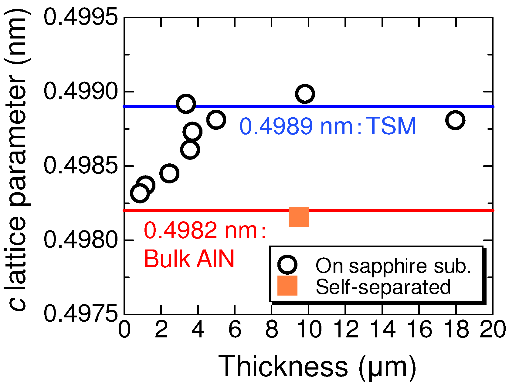
The c lattice parameters in the grown AlN films with various thicknesses were estimated by the XRD 2θ/ω scans. The samples were fabricated under the typical growth conditions described in the previous section, except that the Ar flow rate was varied. The Ar flow rate was changed from 0.25 SLM to 1 SLM, and the respective N2/Al ratios were from 5300 to 1300, leading to variations in the thicknesses (growth rates) [11]. Both Ar and N2 were supplied beginning at room temperature (RT). The XRD φ scans of all the samples confirm six-fold symmetry peaks, demonstrating that the samples are single phase.
Figure 1 shows the results, where the open circles and the closed square express the results for AlN on sapphire and self-separated AlN, respectively.
As described in the next section, self-separation often occurs when N2 is supplied after the substrate temperature reaches the growth temperature, but this self-separated film is created by chance when the N2 supply is initiated at RT. The reason for this peeling is unclear. The c lattice parameter of unstrained AlN is 0.4982 nm, while that for strained AlN due to thermal stress is 0.4989 nm. The latter was calculated using the thermal stress model (TSM) [16,17,18], assuming that the epilayer is fully relaxed at the growth temperature, but then the epilayer is elastically strained during the cooling process due to the thermal expansion mismatch between the epilayer and substrate. The c lattice parameter of AlN on sapphire approaches the TSM values as the film thickness increases, which indicates that the strain originating from the thermal stress remains in the crack-free films on the sapphire substrate (Figure 1). On the other hand, self-separated AlN has a c lattice parameter close to the unstrained value without following the trend of the former; the stress is considered to be almost completely relaxed in self-separated AlN.
3.2. Mechanisms of Interface Formation
Figure 2 illustrates the temperature profiles and flow sequences. Although Ar gas was always supplied beginning at RT, Al metal was placed in the Ar stream in the source zone only when exploring the effect of Al. For N2, we examined two supply sequences. The N2 supply is initiated (1) when the substrate temperature reaches the typical growth temperature of 1550 °C [Process N2(GT)]; or (2) at RT [Process N2(RT)]. (Therefore, the Al + Process N2(RT) is equivalent to the AlN pretreatment detailed in ref. [12].)
Figure 3 shows the cross-sectional images near the AlN/sapphire interfaces grown with Al + (a) Process N2(GT) and (b) Process N2(RT). Both AlN films are about 1-µm thick (growth rate: 1 µm/h). The former has a rough interface, particularly on the AlN side, while the latter has a relatively smooth one on the AlN side with some voids on the sapphire side. Self-separation is frequently observed in the case of Al + Process N2(GT), but is rare in the case of Al + Process N2(RT). Thus, the rough interface on the AlN side causes a self-separation.
To investigate the interface formation mechanisms, the effect of N2 on the sapphire annealing characteristics was examined without supplying Al. (That is, AlN was not grown intentionally). Figure 4 shows the SEM bird’s-eye views, EDS profiles, and XRD profiles of sapphire annealed in atmospheres without N2 (only Ar), with Process N2(GT), and Process N2(RT) at 1550 °C.
The gas flow rates and pressure were the same as those of the standard growth conditions described in Section 2. Annealing without N2 considerably roughens the sapphire surface (Figure 4a). The EDS profiles of the sample (Figure 4d) indicate that the roughened area includes more Al than the flat area, which suggests that the thermal decomposition of sapphire leaves Al-related materials on it. With Process N2(GT), N2 is supplied to such a roughened sapphire surface, and the degree of the roughness is preserved (Figure 4b). Furthermore, N2 may react with the Al-related materials to form AlN polycrystalline grains, as evidenced by the EDS and XRD profiles shown in Figure 4e,g. It is noteworthy that the morphology in Figure 4b is similar to that in Figure 3a, implying that the rough AlN poly-like crystals at the interface play a key role in the self-separation phenomenon. On the other hand, with Process N2(RT), nitridation of sapphire at a relatively low temperature may prevent the decomposition of sapphire. Instead, a considerably thin AlN (or AlON) is generated, as demonstrated by EDS and XRD. The EDS measurement detected a signal attributed to the N element (Figure 4f), but the XRD 2θ-ω profile does not exhibit diffraction peaks due to AlN. It should be noted that the voids observed in Figure 3b are not formed in any of the conditions for this sapphire annealing, suggesting that Al plays an important role in void formation.
To explore the reaction between the Al source and the sapphire substrate, sapphire annealing without N2 was performed. Figure 5 shows SEM bird’s-eye views of the sapphire surfaces annealed in an atmosphere (a) without Al and (b) with Al at 1350 °C for 1 h. (Similar to above, Ar was supplied in both cases.) To reduce the effect of thermal decomposition of sapphire, the annealing temperature was set to 1350 °C. Without an Al supply (Figure 5a), residues are generated on the sapphire surface, similar to Figure 4a, but their size is smaller than that at 1550 °C due to the lower temperature. Annealing with Al creates larger residues than that without Al, suggesting that the Al source contributes to the formation of such a structure. The whisker-like morphology formed by annealing with Al may lead to subsequent AlN whisker growth as reported in ref. [12]. Similar to above, voids are not observed. Thus, the voids are formed only when AlN is grown with Al + Process N2(RT). That is, Al, nitrided sapphire, and suppression of sapphire thermal decomposition are prerequisites.
There are two possible mechanisms for void formation. (A) The nitrided layers of sapphire are not continuous on the surface, and certain regions without nitridation thermally decompose; (B) Al and O from the sapphire diffuse through the nitrided layer after the nitridation of the entire sapphire surface. The likelihood of (A) is low because the morphology of the thermally treated sapphire in an Al ambient (Figure 5b) does not agree with the square shape of the voids observed in cross sections (Figure 3b). Rather, the Al gases supplied to a nitrided sapphire surface diffuse through the nitrided layer and react with sapphire (reduction of sapphire) to form voids. Although specific paths for the diffusion of Al and O are unclear, defects such as threading dislocations can be the paths as reported in ref. [19].
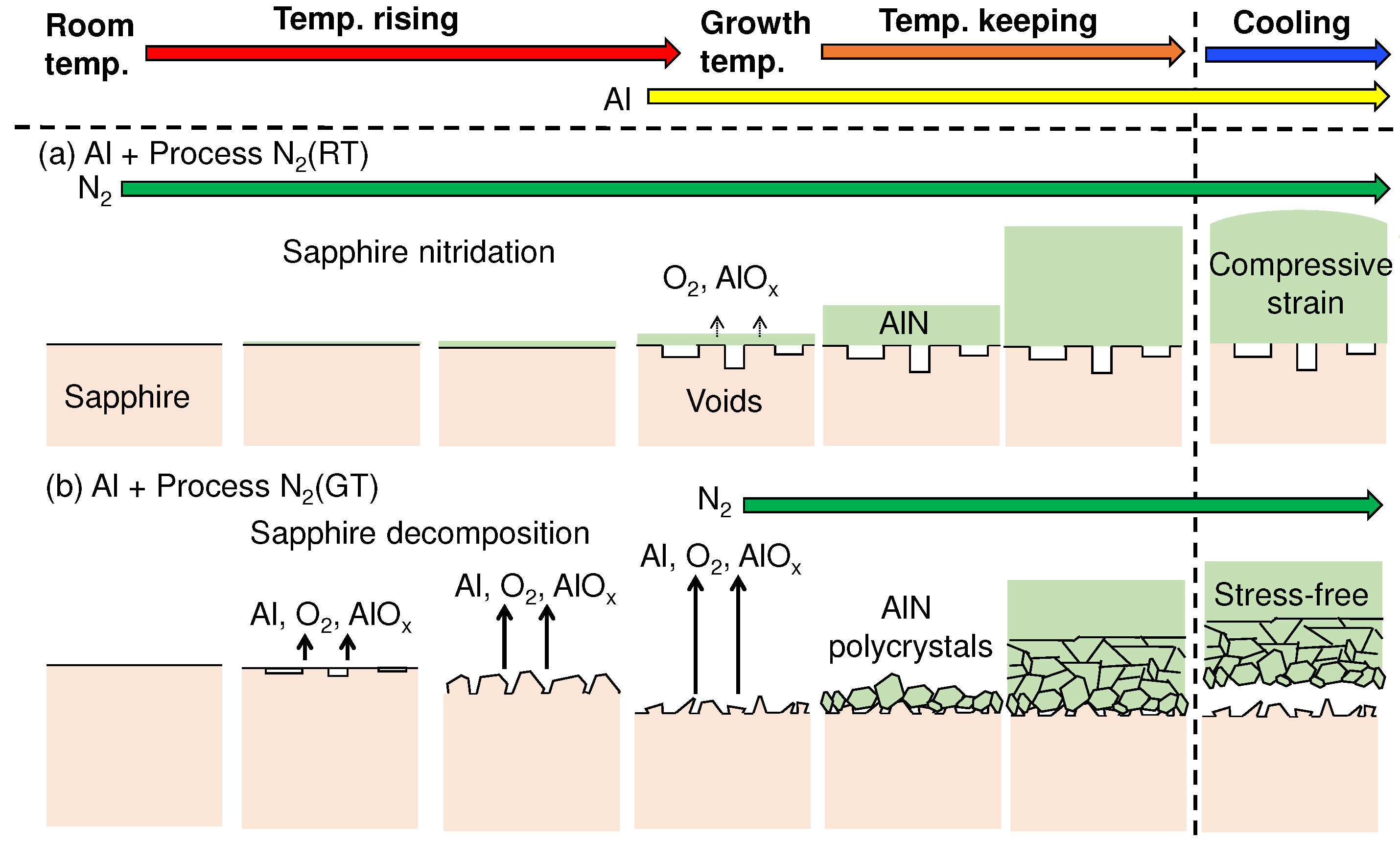
Based on these findings, the possible mechanisms for the interface formation by EVPE are briefly summarized in the schematic illustration shown in Figure 6. In Al + Process N2(GT), the rough sapphire surface due to the thermal decomposition reacts with N2, inducing a rough interface (Figure 6b). This interface separates the epitaxial film from the substrate during post-growth cooling to RT because it is physically weak. On the other hand, in the Al + Process N2(RT) condition, a relatively smooth interface with some voids is formed due to the reaction between the nitrided sapphire surface and Al source.
4. Conclusions
The dependence of the c lattice parameter on thickness indicates that the strain derived from the thermal stress remains in crack-free films on sapphire substrates, but is almost completely relaxed in self-separated films. The SEM cross sectional observations suggest that the self-separated films are generated by the rough interface due to the thermal decomposition of sapphire, but can be controlled by the N2 supply timing. The voids are observed at the interface only when the Al source is supplied on the nitrided sapphire surface, indicating that the reaction between a nitrided sapphire surface and Al source forms the voids.
Acknowledgments
This work is partially supported by JSPS KAKENHI Grant numbers JP16H02332, JP15H05732, and JP16H06426. The authors acknowledge PeiTsen Wu for her assistance with crystal growth.
Author Contributions
Yoichi Kawakami and Mitsuru Funato conceived the project; Katsuhiro Kishimoto and Mitsuru Funato designed and performed the experiments; All authors analyzed the data and wrote the paper.
Conflicts of Interest
The authors declare no conflict of interest.
References
- Bickermann, M.; Filip, O.; Epelbaum, B.M.; Heimann, P.; Feneberg, M.; Neuschl, B.; Thonke, K.; Wedler, E.; Winnacker, A. Growth of AlN bulk crystals on SiC seeds: Chemical analysis and crystal properties. J. Cryst. Growth 2012, 339, 13–21. [Google Scholar] [CrossRef]
- Sumathi, R.R.; Gille, P. Development and progress in bulk c-plane AlN single-crystalline template growth for large-area native seeds. Jpn. J. Appl. Phys. 2013, 52, 08JA02. [Google Scholar] [CrossRef]
- Dalmau, R.; Moody, B.; Xie, J.; Collazo, R.; Sitar, Z. Characterization of dislocation arrays in AlN single crystals grown by PVT. Phys. Stat. Sol. 2011, 208, 1545–1547. [Google Scholar] [CrossRef]
- Lu, P.; Collazo, R.; Dalmau, R.F.; Dulkaya, G.; Dietz, N.; Raghothamachar, B.; Dudley, M.; Sitar, Z. Seeded growth of AlN bulk crystals in m- and c-orientation. J. Cryst. Growth 2009, 312, 58–63. [Google Scholar] [CrossRef]
- Bondokov, R.T.; Mueller, S.G.; Morgan, K.E.; Slack, G.A.; Schujman, S.; Wood, M.C.; Smart, J.A.; Schowalter, L.J. Large-area AlN substrates for electronic applications: An industrial perspective. J. Cryst. Growth 2008, 310, 4020–4026. [Google Scholar] [CrossRef]
- Kumagai, Y.; Kubota, Y.; Nagashima, T.; Kinoshita, T.; Dalmau, R.; Schlesser, R.; Moody, B.; Xie, J.; Murakami, H.; Koukitu, A.; et al. Preparation of a freestanding AlN substrate from a thick AlN layer grown by hydride vapor phase epitaxy on a bulk AlN substrate prepared by physical vapor transport. Appl. Phys. Exp. 2012, 5, 055504. [Google Scholar] [CrossRef]
- Claudel, A.; Fellmann, V.; Gélard, I.; Coudurier, N.; Sauvage, D.; Balaji, M.; Blanquet, E.; Boichot, R.; Beutier, G.; Coindeau, S.; et al. Influence of the V/III ratio in the gas phase on thin epitaxial AlN layers grown on (0001) sapphire by high temperature hydride vapor phase epitaxy. Thin Solid Films 2014, 573, 140–147. [Google Scholar] [CrossRef]
- Gong, X.; Xu, K.; Huang, J.; Liu, T.; Ren, G.; Wang, J.; Zhang, J. Evolution of the surface morphology of AlN epitaxial film by HVPE. J. Cryst. Growth 2015, 409, 100–104. [Google Scholar] [CrossRef]
- Baker, T.; Mayo, A.; Veisi, Z.; Lu, P.; Schmitt, J. Hydride vapor phase epitaxy of AlN using a high temperature hot-wall reactor. J. Cryst. Growth 2014, 403, 29–31. [Google Scholar] [CrossRef]
- Tsujisawa, K.; Kishino, S.; Li, D.-B.; Miyake, H.; Hiramatsu, K.; Shibata, T.; Tanaka, M. Suppression of crack generation using high-compressive-strain AlN/Sapphire template for hydride vapor phase epitaxy of thick AlN film. Jpn. J. Appl. Phys. 2007, 46, L552–L555. [Google Scholar] [CrossRef]
- Wu, P.T.; Funato, M.; Kawakami, Y. Environmentally friendly method to grow wide-bandgap semiconductor aluminum nitride crystals: Elementary source vapor phase epitaxy. Sci. Rep. 2015, 5, 17405. [Google Scholar] [CrossRef] [PubMed]
- Wu, P.T.; Kishimoto, K.; Funato, M.; Kawakami, Y. Control of crystal morphologies and interface structures of AlN grown on sapphire by elementary source vapor phase epitaxy. Cryst. Growth Des. 2016, 16, 6337–6342. [Google Scholar] [CrossRef]
- Banal, R.G.; Akashi, Y.; Matsuda, K.; Hayashi, Y.; Funato, M.; Kawakami, Y. Crack-free thick AlN films obtained by NH3 nitridation of sapphire substrates. Jpn. J. Appl. Phys. 2013, 52, 08JB21. [Google Scholar] [CrossRef]
- Bailar, J.; Emeleus, H.J.; Nyholm, R.; Trotman-Dickerson, A.F. Comprehensive Inorganic Chemistry; Pergamon Press: Oxford, UK, 1973. [Google Scholar]
- Mohn, S.; Stolyarchuk, N.; Markurt, T.; Kirste, R.; Hoffmann, M.P.; Collazo, R.; Courville, A.; Felice, R.D.; Sitar, Z.; Vennegues, P.; et al. Polarity control in group-III nitrides beyond pragmatism. Phys. Rev. Appl. 2016, 5, 054004. [Google Scholar] [CrossRef]
- Matsumoto, T.; Miyaji, Y.; Kiuchi, K.; Kato, T. Chloride multi-source epitaxial growth of CuGaS2 and CuGaSe2. J. Appl. Phys. 1993, 32, 142–144. [Google Scholar] [CrossRef]
- Iwanaga, H.; Kunishige, A.; Takeuchi, S. Anisotropic thermal expansion in wurtzite-type crystals. J. Mater. Sci. 2000, 35, 2451–2454. [Google Scholar] [CrossRef]
- Wim, W.M.; Paff, R.J. Thermal expansion of AlN, sapphire, and silicon. J. Appl. Phys. 1974, 45, 1456–1457. [Google Scholar]
- Kumagai, Y.; Enatsu, Y.; Ishizuki, M.; Kubota, Y.; Tajima, J.; Nagashima, T.; Murakami, H.; Takada, K.; Koukitu, A. Investigation of void formation beneath thin AlN layers by decomposition of sapphire substrates for self-separation of thick AlN layers grown by HVPE. J. Cryst. Growth 2010, 312, 2530–2536. [Google Scholar] [CrossRef]
Figure 1.
Dependence of the c lattice parameter on thickness.

Figure 2.
Temperature profiles and gas flow sequences.
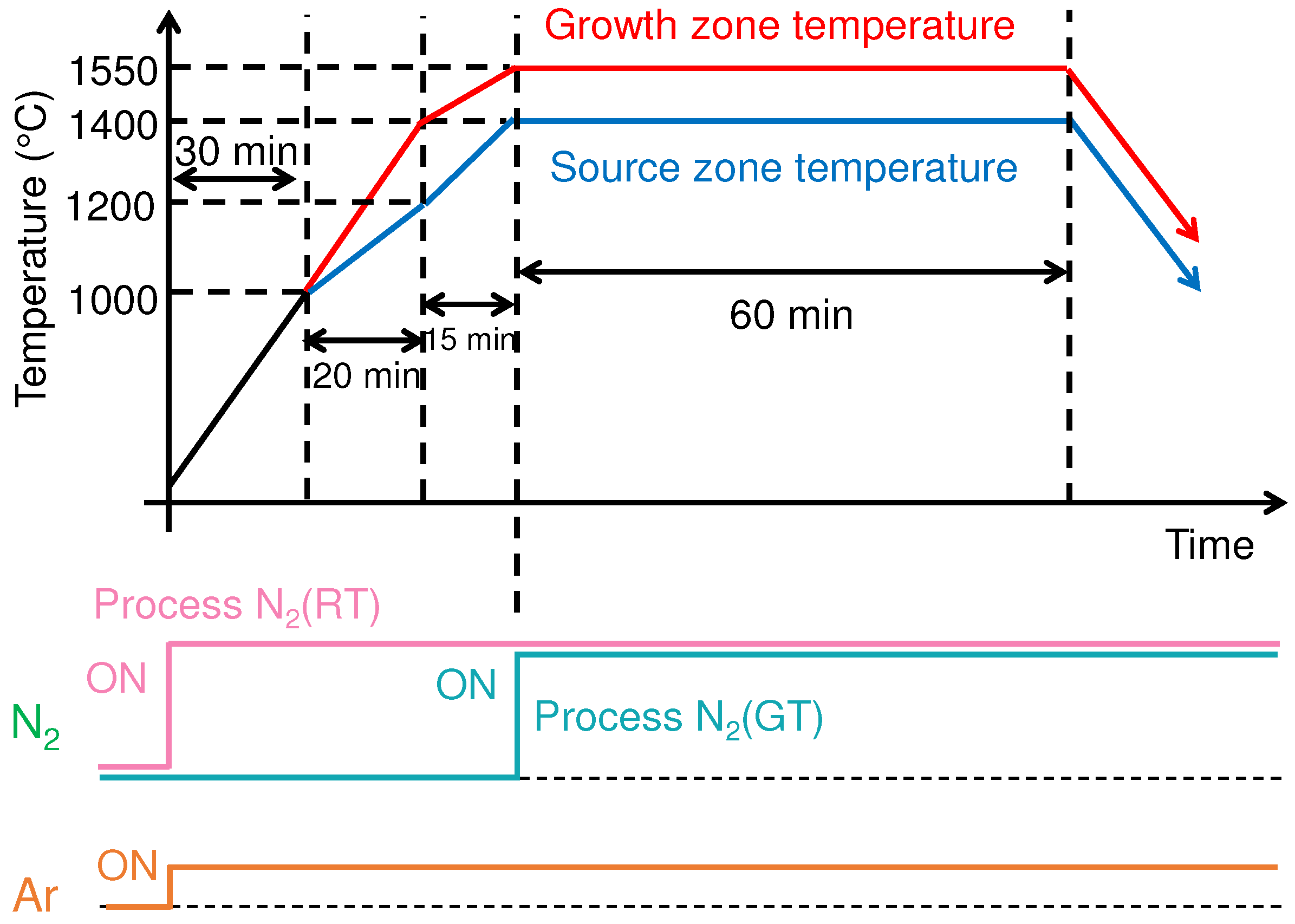
Figure 3.
Cross-sectional images near the interfaces of AlN films on sapphire grown with Al + Processes (a) N(GT) and (b) N(RT).
Figure 3.
Cross-sectional images near the interfaces of AlN films on sapphire grown with Al + Processes (a) N(GT) and (b) N(RT).
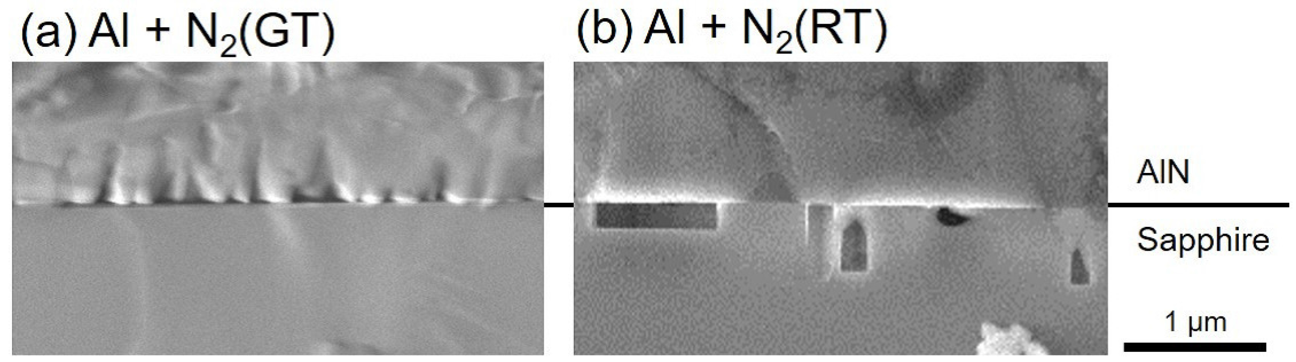
Figure 4.
SEM bird’s-eye views of sapphire surfaces after annealing without Al sources in atmospheres (a) without N (only Ar); (b) with Process N(GT); and (c) with Process N(RT). Respective energy dispersive X-ray spectroscopy (EDS) profiles are displayed in (d–f); (g) XRD - scan profile for sapphire annealed with Process N(GT) in (b).
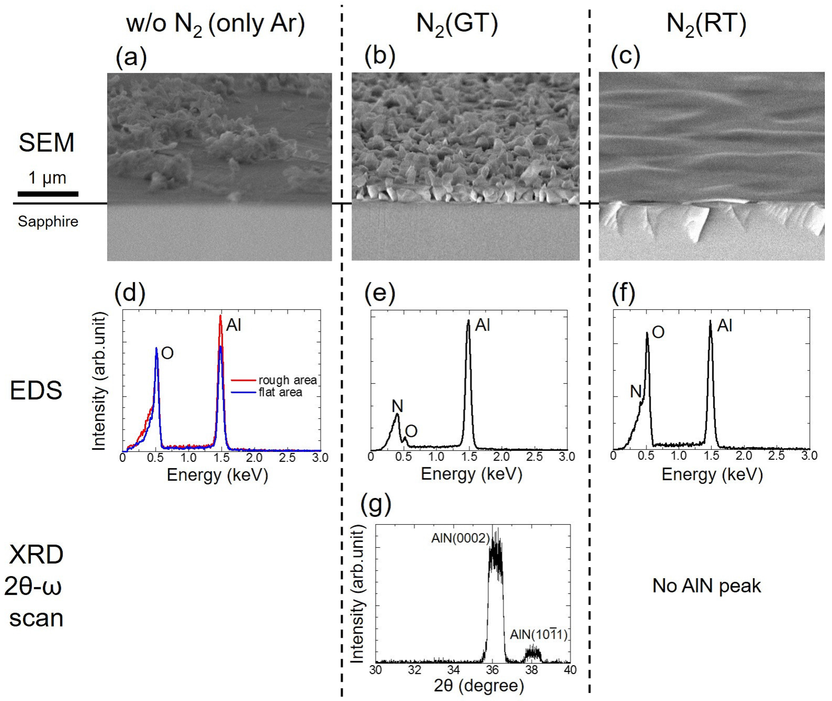
Figure 5.
SEM bird’s-eye views of the sapphire surfaces after annealing without N to examine the effects of Al. (a) Without Al (only Ar) and (b) with Al. In both images, scale bar represents 1 µm.
Figure 5.
SEM bird’s-eye views of the sapphire surfaces after annealing without N to examine the effects of Al. (a) Without Al (only Ar) and (b) with Al. In both images, scale bar represents 1 µm.
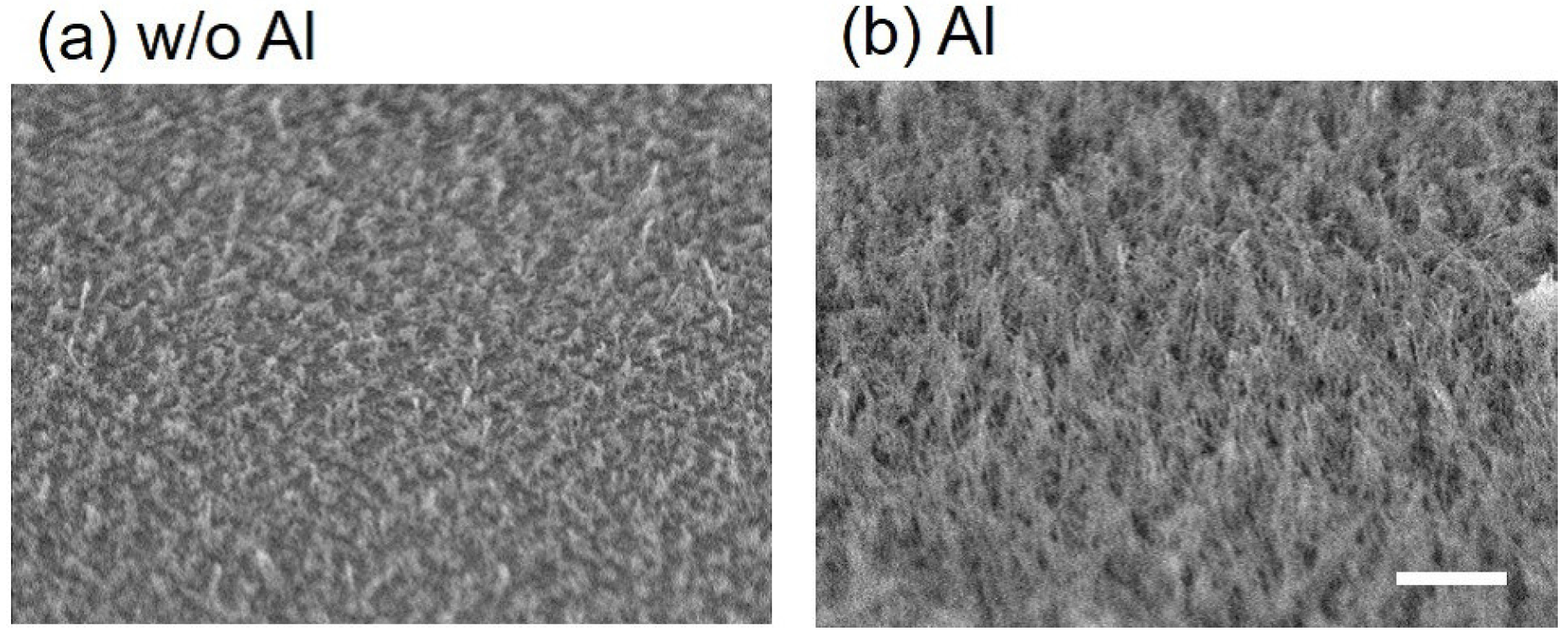
Figure 6.
Proposed interface formation mechanisms in the elementary source vapor phase epitaxy (EVPE) growth with Al + Processes (a) N(GT) and (b) N(RT).
Figure 6.
Proposed interface formation mechanisms in the elementary source vapor phase epitaxy (EVPE) growth with Al + Processes (a) N(GT) and (b) N(RT).

© 2017 by the authors. Licensee MDPI, Basel, Switzerland. This article is an open access article distributed under the terms and conditions of the Creative Commons Attribution (CC BY) license (http://creativecommons.org/licenses/by/4.0/).
Share and Cite
MDPI and ACS Style
Kishimoto, K.; Funato, M.; Kawakami, Y. Effects of Al and N2 Flow Sequences on the Interface Formation of AlN on Sapphire by EVPE. Crystals 2017, 7, 123. https://doi.org/10.3390/cryst7050123
AMA Style
Kishimoto K, Funato M, Kawakami Y. Effects of Al and N2 Flow Sequences on the Interface Formation of AlN on Sapphire by EVPE. Crystals. 2017; 7(5):123. https://doi.org/10.3390/cryst7050123
Chicago/Turabian StyleKishimoto, Katsuhiro, Mitsuru Funato, and Yoichi Kawakami. 2017. "Effects of Al and N2 Flow Sequences on the Interface Formation of AlN on Sapphire by EVPE" Crystals 7, no. 5: 123. https://doi.org/10.3390/cryst7050123
Note that from the first issue of 2016, this journal uses article numbers instead of page numbers. See further details here.