
AlGaN/GaN MOS-HEMTs with Corona-Discharge Plasma Treatment


1
Department of Materials Science and Engineering, National Chung Hsing University, Taichung 402, Taiwan
2
Institute of Electronics, National Chiao Tung University, Hsinchu 300, Taiwan
*
Author to whom correspondence should be addressed.
Crystals 2017, 7(5), 146; https://doi.org/10.3390/cryst7050146
Submission received: 29 April 2017
/
Revised: 13 May 2017
/
Accepted: 16 May 2017
/
Published: 18 May 2017
(This article belongs to the Special Issue Advances in GaN Crystals and Their Applications)
Abstract
:The effects of a corona-discharge plasma treatment on the performance of an AlGaN/GaN metal-oxide-semiconductor high-electron mobility transistor fabricated onto Si substrates were studied. The threshold voltage shifted from −8.15 to −4.21 V when the device was treated with an Al2O3 layer. The leakage current was reduced from 2.9 × 10⁻⁵ to 4.2 × 10⁻⁷ mA/mm, and the ION/IOFF ratio increased from 8.3 × 10⁶ to 7.3 × 10⁸ using the corona-discharge plasma treatment, which exhibited an increase of about two orders of magnitude. The device exhibited excellent performance with a subthreshold swing of 78 mV/dec and a peak gain of 47.92 mS/mm at VGS = 10 V.
1. Introduction
AlGaN/GaN high-electron mobility transistors (HEMTs) are used in high-power, high-frequency applications because they possess properties such as high bulk electron mobility in GaN, a large bandgap, low noise, high thermal control capability, and a high breakdown electric field; furthermore, a high-mobility two-dimensional electron gas (2-DEG) exists at the heterojunction interface [1,2]. To effectively suppress gate leakage, the Schottky gate can be replaced by a metal-oxide-semiconductor (MOS) structure; this allows for the surface state issue to be mitigated via a surface passivation technique [3]. Many oxide materials (e.g., SiO2, Al2O3, HfO2, and La2O3) can be used as the gate oxide layer [4,5,6,7]. Al2O3 simultaneously has a wide bandgap and high relative permittivity. These features make it promising for exploitation in gate oxide applications. In general, MOS-HEMT operates in depletion mode (D-mode) because of thick oxide, cap, and barrier layers. These issues can be resolved by reducing the thickness of the gate oxide layer [8,9,10]. However, the on-resistance increased for MOS-HEMTs when the 2-DEG density reduced along the entire channel [11]. Two methods have been proposed for the fabrication of an enhancement mode (E-mode) operation MOS-HEMT without reducing the 2-DEG density. The two methods are recessed-gate and fluoride-based plasma treatment [12,13]. The aforementioned methods basically treat the local area underneath the gate region. Recessed-gate and fluoride-based plasma treatments depend on inductively coupled plasma reactive ion etching (ICP-RIE) processes that cannot control the etching depth precisely. To resolve the thick layer problem using an etching-free process and without reducing the 2-DEG density, electrons are only implanted through a corona-discharge plasma (CDP) system. CDP treatment is a well-known process often exploited for microphone fabrication. Electrons are implanted onto a dielectric material, thus giving these devices the name “electret condenser microphone” [14]. The electrets act as permanent charge sources, thus an electret condenser microphone can produce a signal without needing any external biasing. This method has several advantages—it is a simple process, is vacuum-free, and is suitable for large-area fabrication. High voltage is applied to the plasma generated in the air to accelerate the electrons from the ionized electrode and control the electrons that travel toward the target using a grid potential. Finally, the electrons are implanted inside the film and become the electret. In this work, the performance of AlGaN/GaN MOS-HEMTs with a CDP-treated (CDPT) GaN cap and oxide layer was studied.
2. Materials and Methods
The AlGaN/GaN MOS-HEMT structures were grown onto 6-in silicon substrates using metalorganic chemical vapor deposition. The device layer comprised a 4.2 µm-thick undoped GaN buffer layer, a 150 nm-thick GaN channel layer, a 31 nm-thick Al0.24Ga0.76N barrier, and a 1.5 nm-thick GaN cap layer. The mesa isolation was in an ICP-RIE system with BCl3/Cl2/Ar. A Ti/Al/Ti/Au (25/125/45/60 nm) metal stack was evaporated onto the source (S) and drain (D) regions. For ohmic contacts, samples were annealed at 850 °C in ambient nitrogen. After the ohmic contact process, a 30 nm Al2O3 layer was deposited using atomic layer deposition at 300 °C. For the final step, Ni/Au (150/60 nm) gate metals were deposited using E-beam evaporation. Two types of CDPT samples were prepared in this study; one was the treated GaN cap layer, and the other was the treated Al2O3 layer; both were treated at 12 kV for 750 s in air. A schematic view of the fabricated AlGaN/GaN MOS-HEMT device and the CDPT system are shown in Figure 1a,b, respectively. The gate length, gate-to-drain, gate-to-source, and source-to-drain distances were LG = 7 µm, LGD = 11 µm, LGS = 2 µm, and LSD = 20 µm, respectively. Reference samples were fabricated on the same wafer without CDPT. The current–voltage (I–V) characteristics of these samples were measured using an B1505 parameter analyzer (KEYSIGHT Technology, Santa Rosa, CA, USA).
3. Results and Discussion
In order to confirm that the thin films become the electrets, contact angles of the GaN and Al2O3 before and after CDPT were measured and are shown in Figure 2. The contact angle was measured by dropping DI-water on the different surface and determining the angle between the films and the tangent to the drop surface. The contact angles of the GaN, CDP-treated GaN, Al2O3, and CDP-treated Al2O3 were 59.97°, 18.93°, 43.37°, and 31.99°, respectively, shown in Figure 2a–d. Obviously, the contact angle can be reduced after CDP treatment. This indicated that the thin films were becoming charged due to the electron implantation.
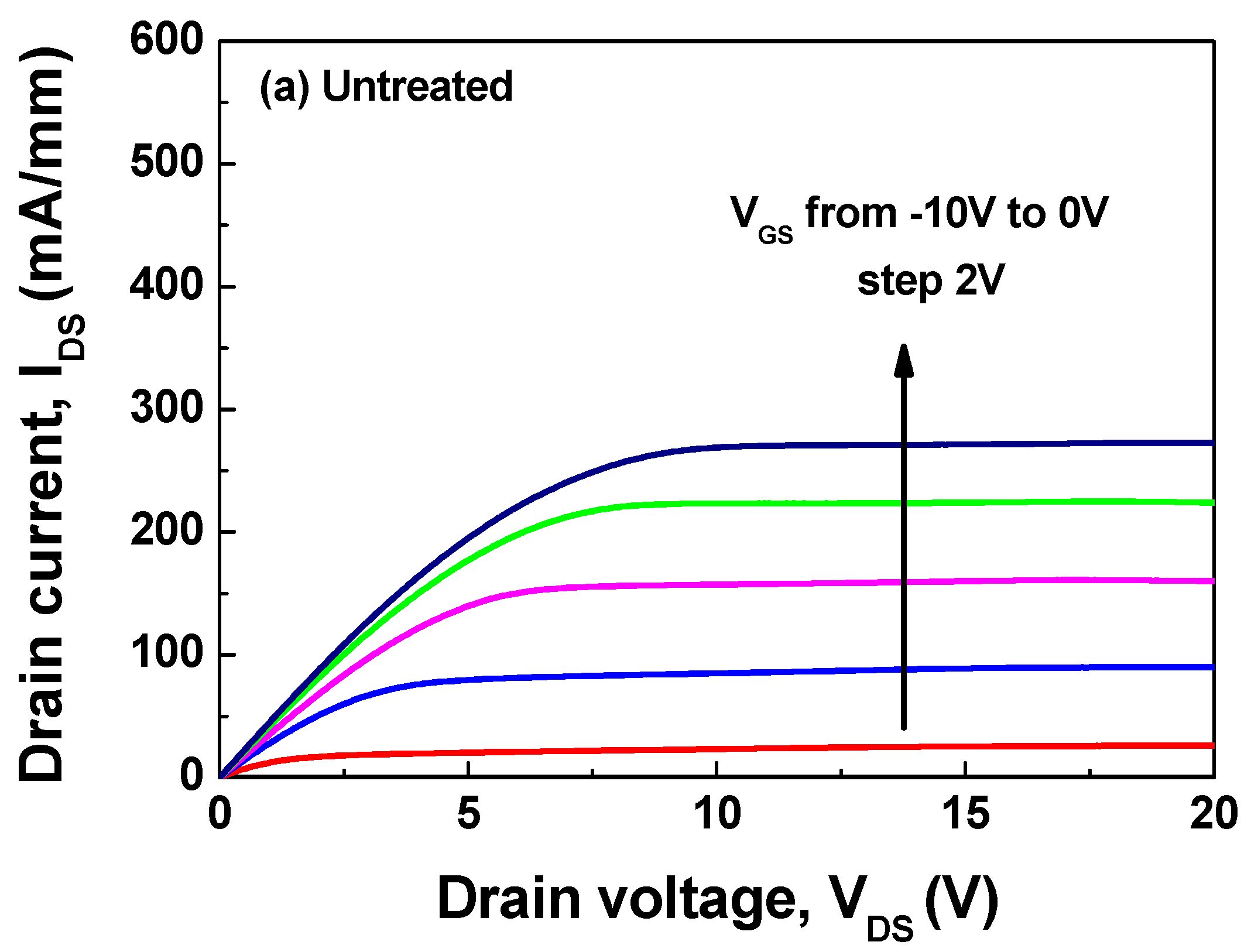
Figure 3 depicts the output characteristics of AlGaN/GaN MOS-HEMTs (a) that were untreated, (b) that had a treated GaN layer, and (c) that had a treated Al2O3 layer. A significant saturation drain current enhancement was observed in the MOS-HEMT containing treated GaN; this can be attributed to an increase in the 2-DEG sheet carrier concentration. This enhancement can be demonstrated using a Hall measurement; Table 1 shows a comparison of the characteristics of the semiconductors of the reference samples and the samples after the corona-discharge plasma treatment. The electron mobility, sheet resistance, and electron concentration were 1550 cm2 V−1·s−1, 549.9 Ω/sq., and 7.34 × 1012 cm−2 for the reference samples, and those for the CDPT samples were 1450 cm2 V−·s−1, 425.7 Ω/sq., and 1.007 × 1013 cm−2, respectively. The sheet concentration increased from 7.341 × 10¹² to 1.007 × 1013 cm−2 for the untreated and treated GaN structures. Nevertheless, the mobility and sheet resistivity were found to be lowered after the corona-discharge plasma treatment.
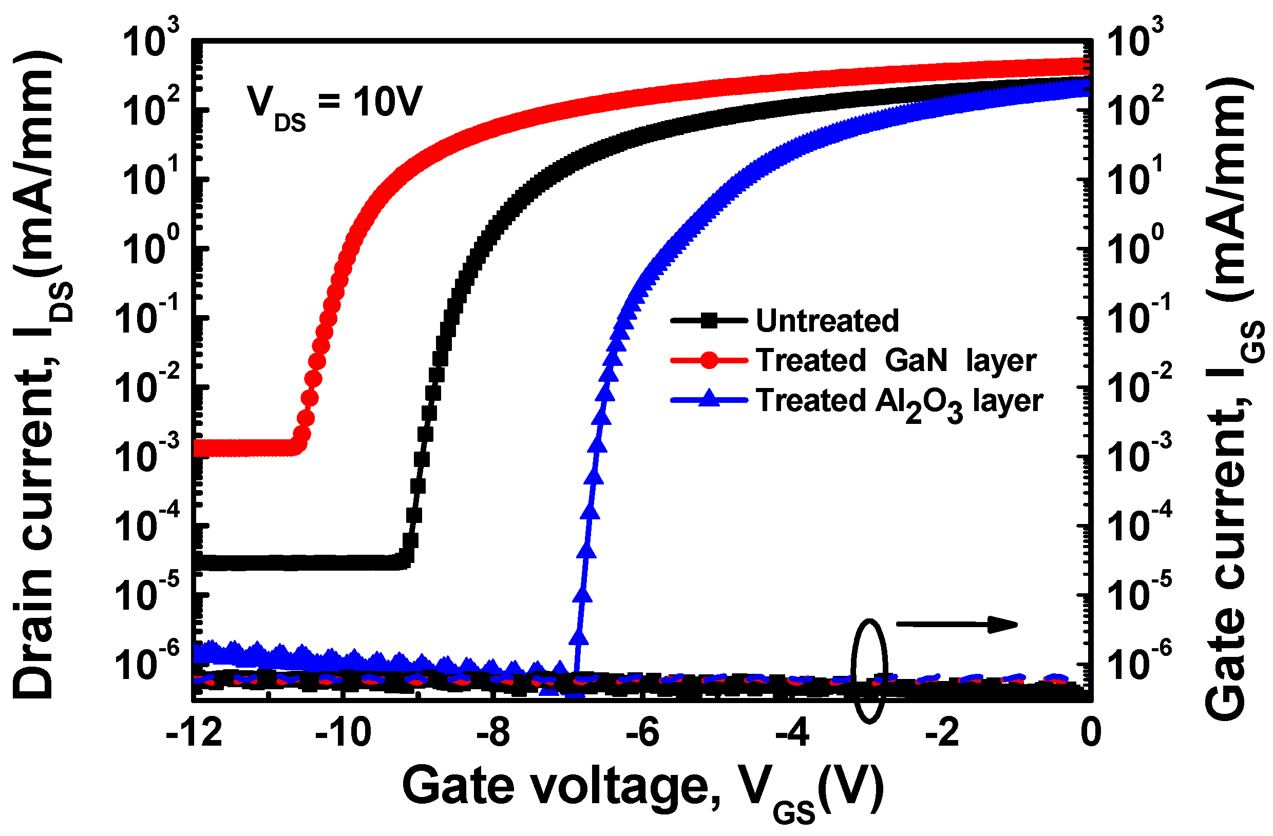
Figure 4 shows the transfer characteristics and transconductance of AlGaN/GaN MOS-HEMTs both with and without CDPT. The threshold voltage (Vth) was extracted by extrapolating the linear part of the transfer curves to zero. The Vth values were −7.19, −8.92, and −4.21 V for the untreated MOS-HEMT, the MOS-HEMT with the treated GaN layer, and the MOS-HEMT with the treated Al2O3 layer, respectively. Vth exhibited a negative shift when the treated GaN layer was used in the MOS-HEMT. In the MOS-HEMT that had not been treated, the Vth shifted positively; this was also the case for the MOS-HEMT with the treated Al2O3 layer. Although these three devices were operating in depletion mode, their Vth values could be tuned depending on which of the three layers CDPT was used on. The maximum transconductance values (gm, max) were 36.08 mS mm−1 for the untreated MOS-HEMT, 53.36 mS mm−1 for the MOS-HEMT with the treated GaN layer, and 47.92 mS mm−1 for the MOS-HEMT with the treated Al2O3 layer.
Figure 5 depicts the AlGaN/GaN MOS-HEMT transfer curves both with and without CDPT at VDS = 10 V. Off-state leakage currents of 2.9 × 10⁻⁵, 1.3 × 10⁻³, and 4.2 × 10⁻⁷ mA/mm were observed for the AlGaN/GaN MOS-HEMTs without treatment, with the treated GaN layer, and with the treated Al2O3 layer, respectively. The off-state current increased when the device was treated using the GaN layer, and it was suppressed when the device was treated using the Al2O3 layer. It is worth mentioning that the three devices exhibited very low leakage currents from the gate to the source; as a result, the influence of the off-state current from the gate current can be ignored. Nevertheless, for the MOS-HEMT with the treated GaN layer, the on–off current (ION/IOFF) ratio decreased from 8.3 × 10⁶ to 3.2 × 10⁵. By contrast, the MOS-HEMT with the treated Al2O3 layer exhibited a significantly better ION/IOFF ratio of 7.3 × 10⁸. Moreover, by comparing the subthreshold swing (SS) of the MOS-HEMTs with the untreated and treated GaN layers, the SS was found to increase significantly from 118 mV dec−1 to 172 mV dec−1; however, the SS decreased to 78 mV dec−1 for the MOS-HEMT with the treated Al2O3 layer.
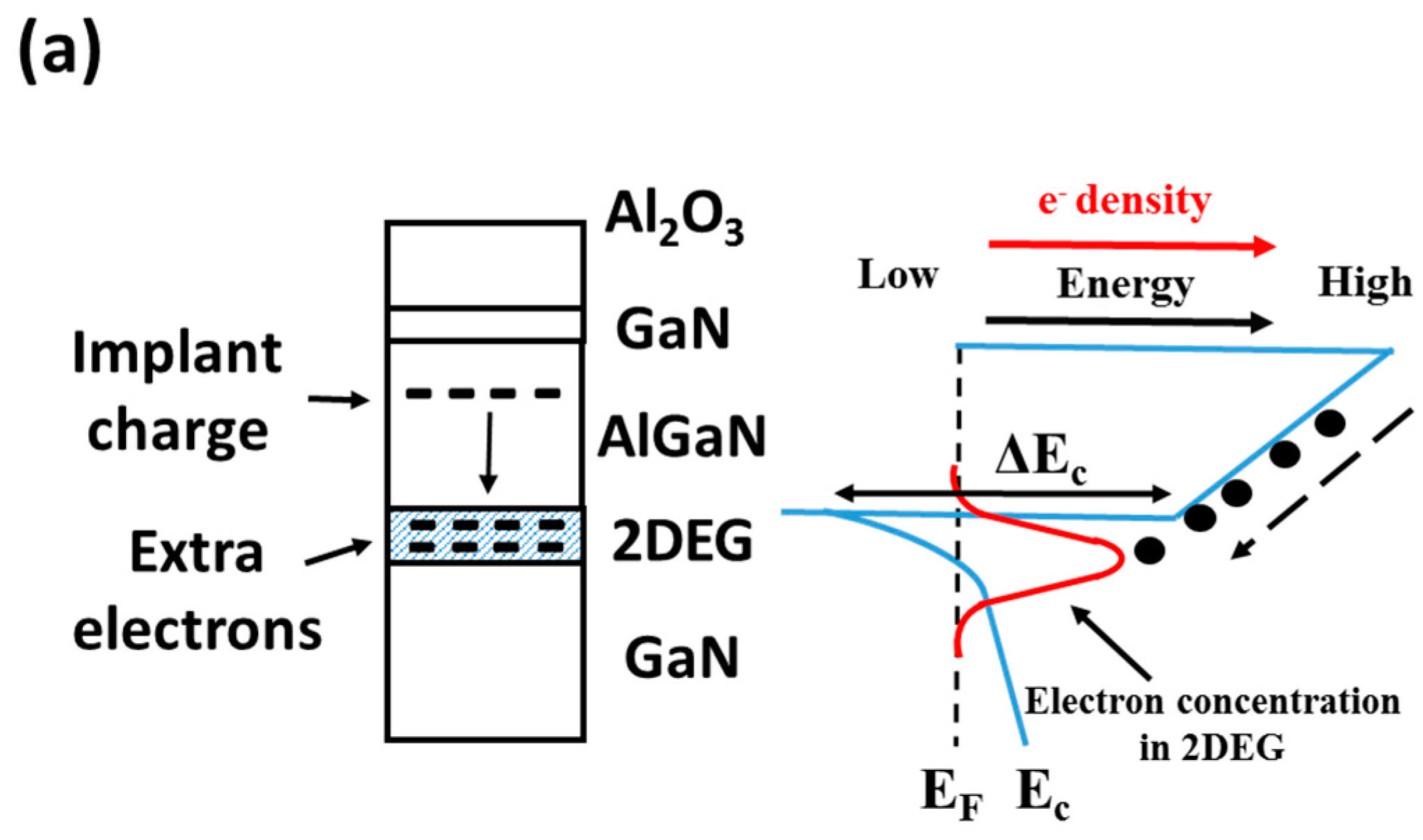
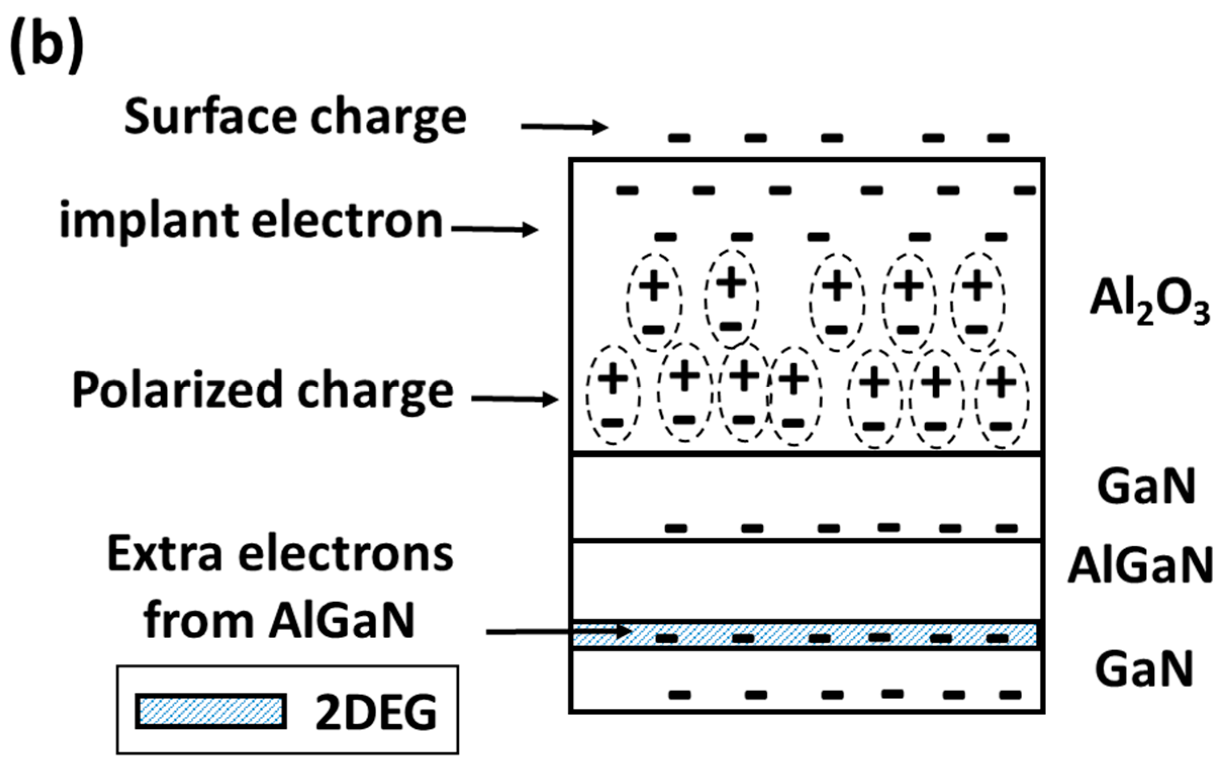
A possible mechanism was proposed for the aforementioned phenomena (shown in Figure 6). For the CDPT-GaN layer, accelerated electrons with high velocity and energy were able to penetrate through the ultra-thin GaN capping layer (1.5 nm) and into the AlGaN barrier layer. These implanted electrons are pushed from the AlGaN layer to the 2-DEG shown in Figure 6a, which results in the 2-DEG electron sheet concentration increasing. As a result, the channel turns on earlier, which results in the threshold voltage shifting negatively. Moreover, this results in the ION and IOFF values increasing. In this case, it could reduce the ION/IOFF ratio for the CDPT-GaN layer as compared with the MOS-HEMT without CDPT. However, for the CDPT gate Al2O3 layer, the accelerated electrons were implanted inside the dielectric and became the electrets. For this gate Al2O3 layer with storage charges, it thus caused a dielectric polarization, as shown in Figure 6b. The dielectric with the electrets had a quasi-permanent dipole polarization and could impart an applied negative voltage. For the MOS-HEMT with the treated Al2O3 layer, the electrons in 2-DEG were repelled by the polarization charges. This resulted in a reduction in the carrier density in 2-DEG. It could reduce IOFF and shift the Vth positively. However, the electrons in the AlGaN barrier layer accumulated at the AlGaN/GaN heterojunction interface owing to the energy barrier. This is demonstrated by the MOS-HEMT with the treated GaN layer having the largest IDS and the MOS-HEMT with the treated Al2O3 layer having the smallest IDS. Although the Vth shifted positively, the MOS-HEMT with the treated Al2O3 layer still presents D-mode operation under the treated parameters (12 KV and 750 s). The magnitude of the accumulated electrons was dependent on the Corona treatment voltage and treatment time. The effect of these parameters on device performance is important and is currently under study.
4. Conclusions
AlGaN/GaN MOS-HEMTs were fabricated onto silicon substrates; threshold voltages were adjusted through CDPT without any gate-recessed etching. The Vth shifted from −7.19 to −8.92 V (negative shift) after GaN cap layer was treated and shifted positively to −4.21 V after the Al2O3 layer was treated. The AlGaN/GaN MOS-HEMT with the treated Al2O3 layer demonstrated excellent channel controllability, which reached an ION/IOFF ratio of 7.3 × 10⁸ and a subthreshold swing of 78 mV/dec. Our experimental results clearly show that a CDPT on an oxide (without thermal annealing or an etching process) is an effective method for fabricating high-performance MOS-HEMTs.
Acknowledgments
This study was financially supported by the Ministry of Science and Technology in Taiwan under contract numbers 104-2221-E-005-031-MY3, 105-3113-E-009-005, and 105-2221-E-005-051-MY3.
Author Contributions
Feng-Yeh Chang, Dong-Sing Wuu, and Ray-Hua Horng conceived the research. All authors analyzed the data, discussed the results for the manuscript. Shuo-Huang Yuan and Ray-Hua Horng wrote the paper.
Conflicts of Interest
The authors declare no conflict of interest.
References
- Ikeda, N.; Niiyama, Y.; Kambayashi, H.; Sato, Y.; Nomura, T.; Kato, S.; Yoshida, S. GaN Power Transistors on Si Substrates for Switching Applications. Proc. IEEE 2010, 98, 1151–1161. [Google Scholar] [CrossRef]
- Lee, D.S.; Gao, X.; Guo, S.P.; Kopp, D.; Fay, P.; Palacios, T. 300-GHz InAlN/GaN HEMTs With InGaN Back Barrier. IEEE Electron Device Lett. 2011, 32, 1525–1527. [Google Scholar] [CrossRef]
- Liu, C.; Chor, E.F.; Tan, L.S. Enhanced device performance of AlGaN/GaN HEMTs using HfO2 high-k dielectric for surface passivation and gate oxide. Semicond. Sci. Technol. 2007, 22, 522. [Google Scholar] [CrossRef]
- Kambayashi, H.; Satoh, Y.; Ootomo, S.; Kokawa, T.; Nomura, T.; Kato, S.; Chow, T.P. Over 100 A operation normally-off AlGaN/GaN hybrid MOS-HFET on Si substrate with high-breakdown voltage. Solid State Electron 2010, 54, 660–664. [Google Scholar] [CrossRef]
- Kanamura, M.; Ohki, T.; Kikkawa, T.; Imanishi, K.; Imada, T.; Yamada, A.; Hara, N. Enhancement-Mode GaN MIS-HEMTs With n-GaN/i-AlN/n-GaN Triple Cap Layer and High-k Gate Dielectrics. IEEE Electron Device Lett. 2010, 31, 189–191. [Google Scholar] [CrossRef]
- Tian, F.; Chor, E.F. Improved Electrical Performance and Thermal Stability of HfO2 / Al2O3 Bilayer over HfO2 Gate Dielectric AlGaN/GaN MIS–HFETs. J. Electrochem. Soc. 2010, 157, H557. [Google Scholar] [CrossRef]
- Chen, J.; Kawanago, T.; Wakabayashi, H.; Tsutsui, K.; Iwai, H.; Nohata, D.; Nohira, H.; Kakushima, K. La2O3 gate dielectrics for AlGaN/GaN HEMT. Microelectron. Reliab. 2016, 60, 16–19. [Google Scholar] [CrossRef]
- Zhang, Y.; Sun, M.; Joglekar, S.J.; Fujishima, T.; Palacios, T. Threshold voltage control by gate oxide thickness in fluorinated GaN metal-oxide-semiconductor high-electron-mobility transistors. Appl. Phys. Lett. 2013, 103, 033524. [Google Scholar] [CrossRef]
- Asgari, A.; Kalafia, M.; Faraone, L. The effects of GaN capping layer thickness on two-dimensional electron mobility in GaN/AlGaN/GaN heterostructures. Phys. E Low Dimens. Syst. Nanostruct. 2005, 25, 431–437. [Google Scholar] [CrossRef]
- Saito, W.; Kuraguchi, M.; Takada, Y.; Tsuda, K.; Omura, I.; Ogura, T. High breakdown Voltage undoped AlGaN-GaN power HEMT on sapphire substrate and its demonstration for DC-DC converter application. IEEE Trans. Electron Devices 2004, 51, 1913–1917. [Google Scholar] [CrossRef]
- Hashizume, T.; Anantathanasarn, S.; Negoro, N.; Sano, E.; Hasegawa, H.; Kumakura, K.; Makimoto, T. Al2O3 Insulated-Gate Structure for AlGaN/GaN Heterostructure Field Effect Transistors Having Thin AlGaN Barrier Layers. Jpn. J. Appl. Phys. 2004, 43, L777. [Google Scholar] [CrossRef]
- Abermann, S.; Pozzovivo, G.; Kuzmik, J.; Strasser, G.; Pogany, D.; Carlin, J.F.; Grandjean, N.; Bertagnolli, E. MOCVD of HfO2 and ZrO2 high-k gate dielectrics for InAlN/AlN/GaN MOS-HEMTs. Semicond. Sci. Technol. 2007, 22, 1272–1275. [Google Scholar] [CrossRef]
- Jiang, R.; Shen, X.; Chen, J.; Duan, G.X.; Zhang, E.X.; Fleetwood, D.M.; Schrimpf, R.D.; Kaun, S.W.; Kyle, E.C.H.; Speck, J.S.; et al. Degradation and annealing effects caused by oxygen in AlGaN/GaN high electron mobility transistors. Appl. Phys. Lett. 2016, 109, 023511. [Google Scholar] [CrossRef]
- Hsieh, W.H.; Hsu, T.Y.; Tai, Y.C. A Micromachined Thin-Film Teflon Electret Microphone. In Proceedings of the International Conference on Solid-state Sensors and Actuators, Chicago, IL, USA, 16–19 June 1997. [Google Scholar]
Figure 1.
(a) Cross-sectional structure of the AlGaN/GaN metal-oxide semiconductor high-electron mobility transistor (MOS-HEMT) and (b) the corona-discharge plasma treatment system. D: drain; G: gate; S: source.
Figure 1.
(a) Cross-sectional structure of the AlGaN/GaN metal-oxide semiconductor high-electron mobility transistor (MOS-HEMT) and (b) the corona-discharge plasma treatment system. D: drain; G: gate; S: source.
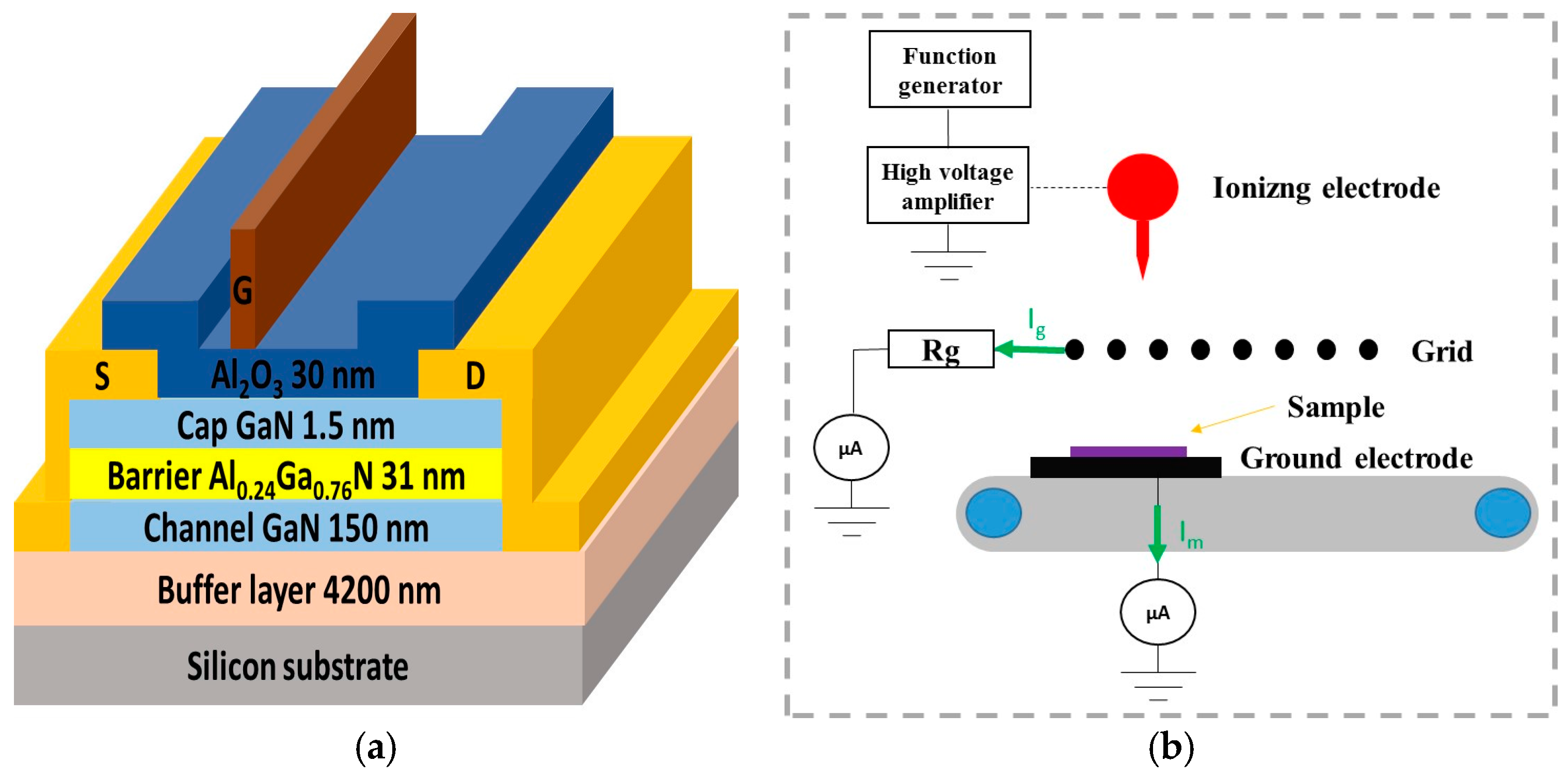
Figure 2.
Contact angle of DI water performed on (a) GaN; (b) corona-discharge plasma (CDP)-treated GaN; (c) Al2O3; and (d) CDP-treated Al2O3.
Figure 2.
Contact angle of DI water performed on (a) GaN; (b) corona-discharge plasma (CDP)-treated GaN; (c) Al2O3; and (d) CDP-treated Al2O3.
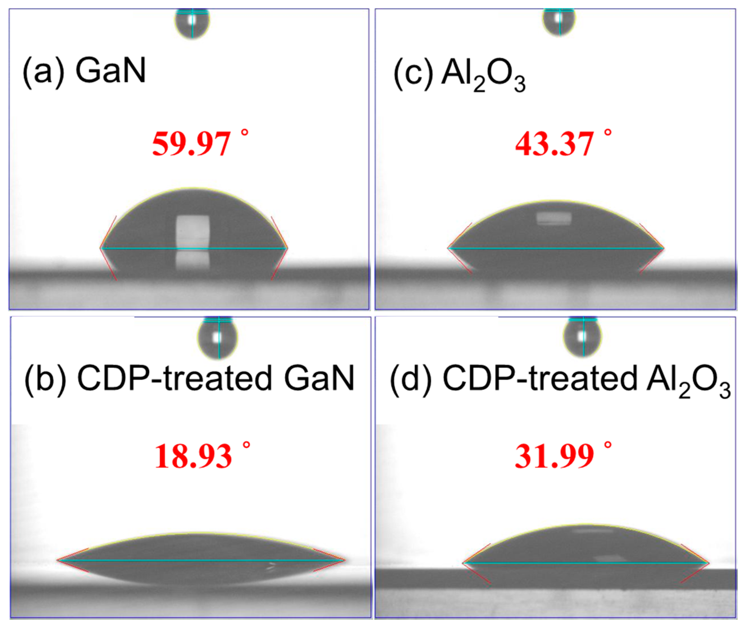
Figure 3.
IDS–VDS output characteristics of the MOS-HEMT: (a) untreated; (b) with a treated GaN; and (c) with a treated Al2O3 layer.
Figure 3.
IDS–VDS output characteristics of the MOS-HEMT: (a) untreated; (b) with a treated GaN; and (c) with a treated Al2O3 layer.

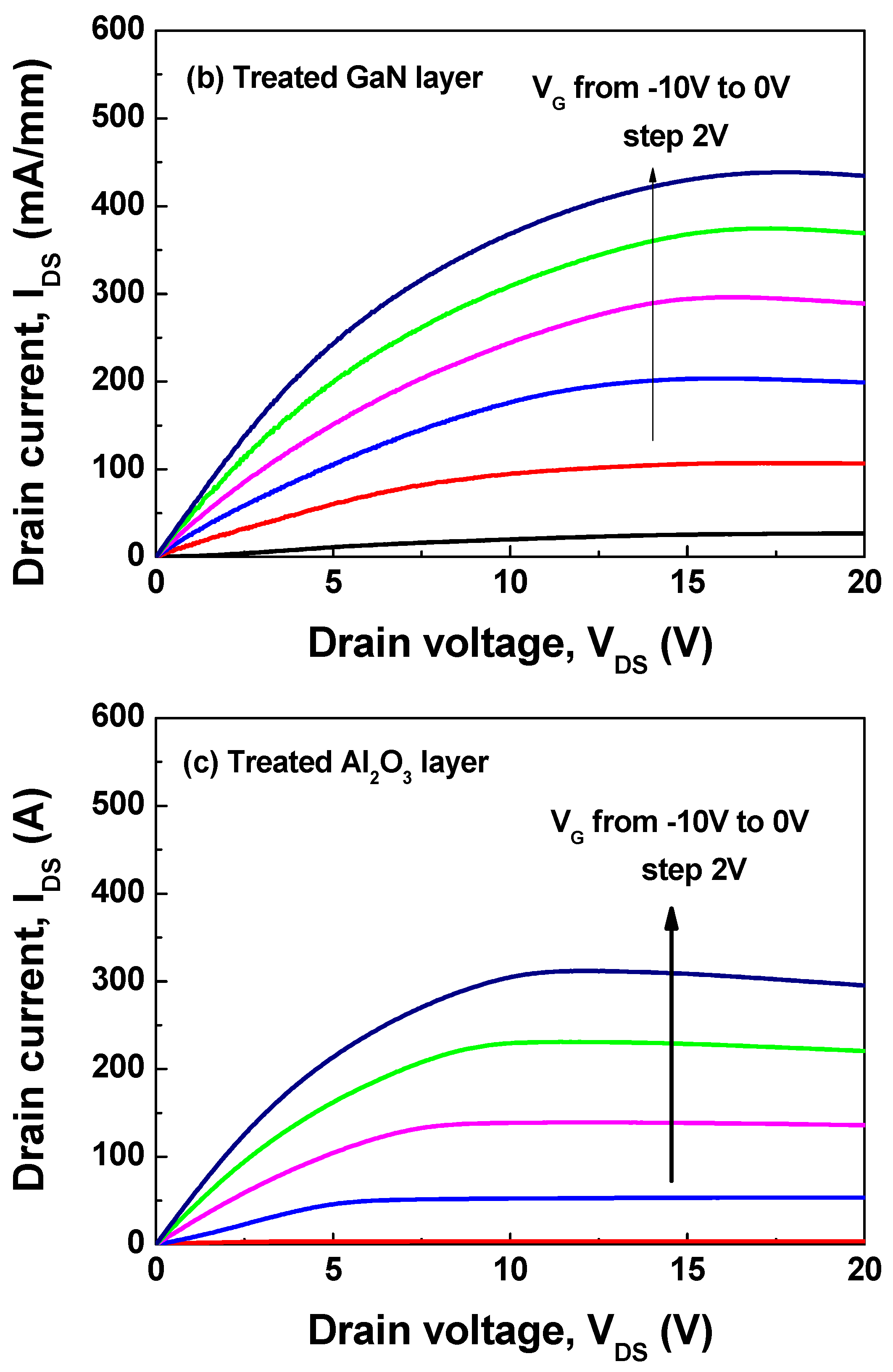
Figure 4.
(a) IDS–VGS and (b) and gm–VGS transfer characteristics of the MOS-HEMT devices with and without the corona-discharge plasma treatment measured at VDS = 10 V.
Figure 4.
(a) IDS–VGS and (b) and gm–VGS transfer characteristics of the MOS-HEMT devices with and without the corona-discharge plasma treatment measured at VDS = 10 V.
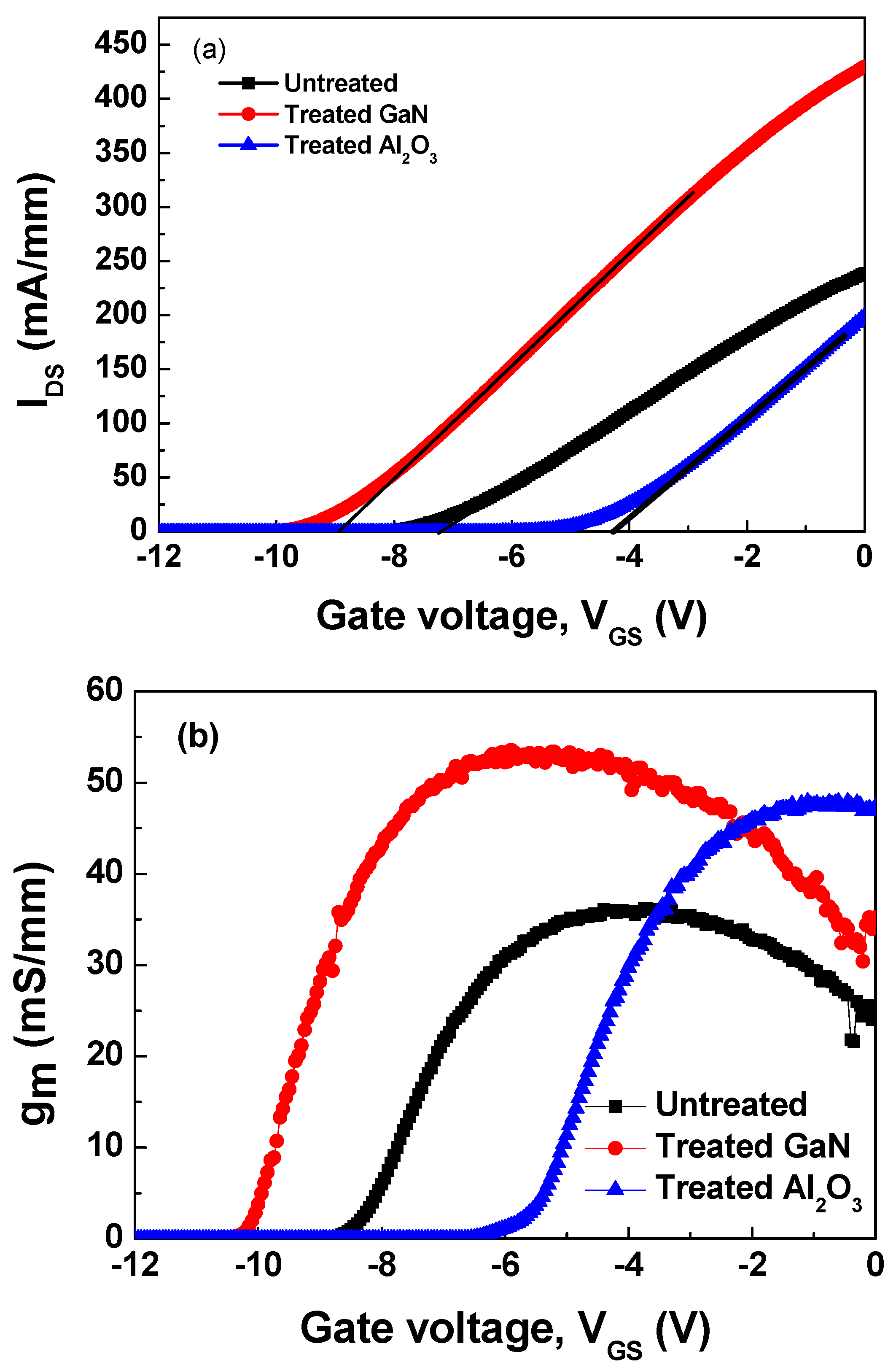
Figure 5.
Transfer characteristics of AlGaN/GaN MOS-HEMT: untreated, with a treated GaN layer, and with a treated Al2O3 layer.
Figure 5.
Transfer characteristics of AlGaN/GaN MOS-HEMT: untreated, with a treated GaN layer, and with a treated Al2O3 layer.

Figure 6.
Mechanism of CDP treatment (CDPT) on (a) GaN and (b) Al2O3 layers.

Table 1.
Comparison of the characteristics of the semiconductor before and after the corona discharge plasma treatment.
Table 1.
Comparison of the characteristics of the semiconductor before and after the corona discharge plasma treatment.
| Characteristics | Reference | 12 KV-750 s |
|---|---|---|
| Sheet concentration (1/cm2) | 7.341 × 10¹² | 1.007 × 10¹³ |
| Mobility (cm2/V-s) | 1550 | 1450 |
| Sheet resistivity (Ω/□) | 549.9 | 425.7 |
© 2017 by the authors. Licensee MDPI, Basel, Switzerland. This article is an open access article distributed under the terms and conditions of the Creative Commons Attribution (CC BY) license (http://creativecommons.org/licenses/by/4.0/).
Share and Cite
MDPI and ACS Style
Yuan, S.-H.; Chang, F.-Y.; Wuu, D.-S.; Horng, R.-H. AlGaN/GaN MOS-HEMTs with Corona-Discharge Plasma Treatment. Crystals 2017, 7, 146. https://doi.org/10.3390/cryst7050146
AMA Style
Yuan S-H, Chang F-Y, Wuu D-S, Horng R-H. AlGaN/GaN MOS-HEMTs with Corona-Discharge Plasma Treatment. Crystals. 2017; 7(5):146. https://doi.org/10.3390/cryst7050146
Chicago/Turabian StyleYuan, Shuo-Huang, Feng-Yeh Chang, Dong-Sing Wuu, and Ray-Hua Horng. 2017. "AlGaN/GaN MOS-HEMTs with Corona-Discharge Plasma Treatment" Crystals 7, no. 5: 146. https://doi.org/10.3390/cryst7050146
Note that from the first issue of 2016, this journal uses article numbers instead of page numbers. See further details here.