Thick Hydride Vapor Phase Heteroepitaxy: A Novel Approach to Growth of Nonlinear Optical Materials

Air Force Research Laboratory, Sensors Directorate, WPAFB, Dayton, OH 45433, USA
*
Author to whom correspondence should be addressed.
Crystals 2019, 9(8), 393; https://doi.org/10.3390/cryst9080393
Submission received: 20 June 2019
/
Revised: 23 July 2019
/
Accepted: 25 July 2019
/
Published: 30 July 2019
(This article belongs to the Special Issue Hydride Vapor Phase Epitaxy Growth of Crystals)
Abstract
:At the time when many nonlinear optical (NLO) materials for frequency conversion of laser sources in the mid and long-wave infrared have achieved their fundamental or technological limits, we propose heteroepitaxy as a solution to develop novel NLO materials. Heteroepitaxy, is the most applied method to combine two different materials—by growing one material on another. In this work we show that combining two binary materials in a ternary may significantly improve the NLO properties that are of great importance for the pursued applications. Plus, due to the closer lattice match to the related substrate, a ternary is always a more favorable heteroepitaxial case than the two completely different materials. We also discuss combining different growth methods—one close-to-equilibrium (e.g., hydride vapor phase epitaxy—HVPE) with one far-from-equilibrium (e.g., metal organic chemical vapor deposition (MOCVD) or molecular beam epitaxy (MBE)) growth processes—to explore new opportunities for the growth of novel heterostructures, including ternary layers with gradual change in composition. The combination of different materials by nature—organics with inorganics—in a hybrid quasi-phase matching (QPM) structure is another topic we briefly discuss, along with some innovative techniques for the fabrication of orientation-patterned (OP) templates, including such that are based on the most universal semiconductor material—Si. Still, the focus in this work is on a series of NLO materials—GaAs, GaP, ZnSe, GaSe, ZnTe, GaN… and some of their ternaries grown with high surface and crystalline quality on non-native substrates and on non-native OP templates using hydride vapor phase epitaxy (HVPE). The grown thick device quality QPM structures were used for further development of high power, compact, broadly tunable frequency conversion laser sources for the mid and longwave infrared with various applications in defense, security, industry, medicine and science.
1. Introduction
Despite the huge number of commercially available direct laser sources [1] some wavelength regions still remain barely populated. In such cases, up or down frequency conversion based on wave mixing processes such as second harmonic generation through phase or quasi-phase matching (QPM) in nonlinear optical (NLO) materials could be a solution. The mid and longwave infrared is an example of such regions, as the two atmospheric windows of transparency between 2–5 μm and 8–12 μm are ranges of special interest. The goal of the sources development in this case is to cover the two atmospheric windows of transparency by one single device. At present, however, only a few direct laser sources based on lead salt compounds (PbxSn1−xTe and PbxEu1−xSeyTe1−y) [2] and few quantum cascade lasers [3] can barely provide such spectral coverage. These sources, however, rely on fairly small bandgap transitions and thus produce modest output power—not enough for the pursued applications. In addition, such sources are hardly tunable and in some cases require cryogenic temperatures to operate efficiently. Thus new developments of frequency conversion coherent sources are highly desirable and motivated by potential applications in security (airport scanners, remote sensing of chemicals (explosives and biological agents)), defense (aircraft protection, laser radar, high-speed IR communications), industry (gas sensing, leak detection, pollution monitoring, process control), science (infrared spectroscopy) and medicine (medical imaging, biopsy-free cancer detection).
The attempts in this direction started with phase matching in birefringent crystal materials such as AgGaSe2, ZnGeP2 [4] and KTP (potassium titanyl phosphate—KTiOPO4). However, problems such as thermal lensing, beam walk-off and low damage threshold turned the attention to compensating the phase velocity dispersion by QPM.
The first practical realization of QPM frequency conversion was realized in ferroelectric periodically poled LiNbO3 (PPLN), which strong intrinsic absorption, however, limited its usage to wavelengths below 4 μm [5]. In non-ferroelectric materials, such as the zinc blended GaAs, GaP or ZnSe, the spatially inverting of the nonlinear susceptibility can be achieved with a periodic structure of alternating crystal domains, grown on a thin micro-structured material called the orientation-patterned (OP) template. GaAs with its broad IR transparency (Figure 1a and Table 1), high NLO susceptibility (Table 1), mature growth and template preparation techniques, and demonstrated 60% conversion efficiency [6,7,8] could be considered as the most successful OP nonlinear material today. Its strong two-photon absorption (2PA; Figure 1b) at wavelengths below 1.7 μm [9] deprives GaAs of using a number of readily available high-power pump laser sources in the range of 1–1.7 μm.
In contrast, the same structured GaP has in the same (1–1.7 μm) spectral range much smaller 2PA coefficient β (Table 1 and Figure 1b). GaP has twice larger thermal conductivity than GaAs, lower thermal expansion (Table 1) and a broad transparency range that starts conveniently in the visible region (Table 1) [10]—the latter allows an easy alignment of the optics during the related optical and NLO measurements. Another advantage of GaP is its smaller refractive index (Table 1) that allows larger domain width of the pattern (Figure 11c). The latter facilitates maintaining the domain fidelity during the thick hydride vapor phase epitaxy (HVPE) growth. All this indicated that GaP is a promising material, until it was realized that the GaP wafer market is much narrower, which means that the price of GaP wafers is much higher, while their quality (in terms of etch pit density (EPD) and wafer parallelism) is much lower. As a consequence the quality of the fabricated OP templates was expected to be lower and from here the follow-on thick growth on such templates results in poor quality. In addition GaP possesses an additional absorption band between 2–4 μm, which, according to [12], is due to free carriers—an issue that can be resolved by in-situ doping of the growing GaP layer with Si [13].
Nevertheless, some progress in the growth of OP-GaP was also achieved [13,14,15,16]. However, due to the low crystalline quality and relatively poor domain fidelity the first results on frequency conversion efficiency in OP-GaP [17] was limited to the range of a few percent only. Improvements in the material quality were, obviously, necessary.
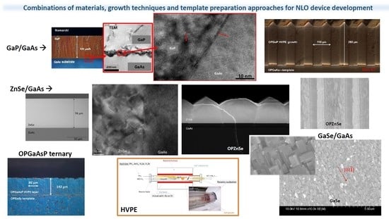
The fact is that neither OP-GaAs nor OP-GaP could achieve the desired efficiency for frequency conversion devices, that neither one is good enough on its own. Thus combining these two materials by growing heteroepitaxially GaP on the readily available high quality OP-GaAs templates seemed logical. These attempts turned out to be successful [18,19,20] in spite of the relatively large negative lattice mismatch (−3.6%) between GaP and GaAs.
The attempts to compensate the lattice mismatch between GaP and GaAs by growing an intermediate GaAsxP1−x ternary buffer layer with a gradually changing x-composition naturally led to the idea for thick growth of GaAsxP1−x ternaries with different compositions. Ternaries are another way to combine two materials in order to combine in one structure their best NLO properties, in this case, the larger non-linear susceptibility of GaAs with the lower 2PA of GaP. Another advantage of such growths is that a ternary has closer lattice match to the related substrate than the two completely different materials. In this point of view, a GaAsxP1−x ternary can be grown on both, GaAs or GaP substrates with a proper x-composition.
Achieving a better understanding of the complex growth and strain relief mechanisms [18,20] during GaP/GaAs heteroepitaxy allowed us to predict other potentially successful heteroepitaxial cases. Some of these cases, due to their smaller lattice mismatches, are even more favorable than GaP/GaAs. Such are, for example, ZnSe/GaAs (+0.238% lattice mismatch), ZnTe/GaSb (+0.083% lattice mismatch) and cubic α-GaSe/GaP (−0.607% lattice mismatch). In many of these cases heteroepitaxy is the only option as large area crystalline substrates are not available on the market [21]. However, in others—similar to the GaP/GaAs case—heteroepitaxy could be preferred again due to purely technological reasons. For example, bulk growth of GaSe is possible, but GaSe is a soft material that hardly could handle the polishing and etching procedures associated with the preparation of an OP template. This means that the eventual growth of OP-GaSe should rely on foreign OP templates such as OP-GaP or OP-GaAs templates. At the same time by using different substrates, the substrate itself can determine the phase of the growing layer, if the material has more than one phase. For example, GaP as a substrate would be a good match to the growth of the cubic α-phase gallium selenide (α-Ga4Se6), while the growth of the hexagonal β-phase gallium selenide (GaSe) must be pursued rather on hexagonal substrates such as GaN.
The exploration of new NLO materials is motivated mostly by the possibility to achieve new frequency ranges, which means new potential applications. However, the choice of a new material is also restricted from the availability of good quality native OP templates. In contrast to the III-nitrides, where comprehensive studies of the polarity control [22,23] led to the development of flexible OP template preparation techniques [24,25], the preparation of OP templates based on III-V compounds is still expensive and difficult procedure. Practically, it is restricted to only two major template preparation approaches—the molecular beam epitaxy (MBE) assisted polarity inversion technique [26] and the wafer fusion (or wafer bonding) technique [27]. While the first one needs expensive MBE equipment, the second one is accompanied by precise and time consuming polishing and etching procedures. As a result the market for OP templates is extremely narrow, while the OP templates are extremely expensive. For example, the cost of a 2-inch or 3-inch GaAs wafer is about $100 USD, while the cost of an OP-GaAs template is about $10,000. Searching for a solution, we present in this article some of our more efficient and less expensive approaches for OP-GaP and OP-GaAs template preparation, including on the most universal semiconductor material—Si [28]. The latter approach is based on the successful combination of two growth processes—one close-to-equilibrium with one far-from-equilibrium.
Attempts to replace the OP templates with the much simpler half-patterned (HP) templates [20] are also described. Some efforts for growth or preparation of QPM structures, including hybrid organic–inorganic QPM structures, without using any patterned templates are also presented [29].
A small section in this article is reserved for a special case heteroepitaxy—Van-der-Waals heteroepitaxy [30] of low-dimensional semiconductor materials such as GaSe.
2. Some Basics of Heteroepitaxy
2.1. The Three Modes of Heteroepitaxy
Heteroepitaxy, i.e., the growth of a crystalline film on a crystalline substrate of a different material, is influenced mostly by their lattice mismatch , which is defined as the relative difference between the lattice constants of the growing film and the substrate :
The lattice mismatches between some of the most popular NLO materials—subject of this article—are given in Table 2. According to [31], one can distinguish three major modes of heteroepitaxy—the two-dimensional (2D) layer-by-layer growth—called also the Frank–Van der Merwe (FM) mode, the three-dimensional (3D) island growth, known as the Volmer–Weber (VW) mode and a special intermediate growth mode, which at certain growth conditions the 2D layer-by-layer growth could convert into (3D) island growth—this is the so-called layer-plus-island, known also as the Stranski–Krastanov (SK) growth mode. Which growth mode will take place during the deposition process depends on many factors among which are the sign and the magnitude of the lattice mismatch between the substrate and the growing layer, and the applied growth conditions. The latter (the applied growth conditions) determines what type of growth we have—far or close to equilibrium from one side, or thermodynamically, kinetically or diffusion limited from another. In the thermodynamic point of view what type of growth we have—FM, VW or SK mode—it depends on the gradient of the chemical potential μ in the direction of growth. Being a derivative of the free Gibbs energy the physical meaning of the chemical potential is the work that should be done (in the particular case of vapor phase epitaxy) to increase the number of particles in the phase with lower energy level (the crystalline layer) at the expense of the number of particles in the phase with the higher energy level—the vapor. This means that when an atom “freezes” (crystalizes) on the substrate surface, leaving the vapor, a portion of energy adequate to the work of formation/separation ψ must be released. In the case of layer-by-layer (2D) growth the thickness gradient of the chemical potential is > 0 (Figure 2a). This means that with thickness increase more work must be done to deliver a particle to the growing layer, i.e., more energy will be released, which is thermodynamically the more favorable case. This layer-by-layer growth (FM) can take place when the lattice mismatch is small and the layer wets nearly completely the substrate (Figure 2a). In the opposite case of island (3D) growth (VW) < 0, which means that with an increase of the layer thickness the growth is getting easier, which also means that with the thickness increase less and less energy of formation will be released, because some of that energy has been, in the meantime, spent in forming the islands. This is an energetically less favorable case that can occur practically at any mismatch if the growing layer wets poorly, i.e., incompletely the substrate (Figure 2b). In the case of the layer-plus-island (SK) mode, the growth starts with layer-by-layer (2D) growth when > 0 during which the film is forced at the beginning to grow with the lattice constant of the substrate on the expense of a linearly increased elastic strain. However, after a certain thickness, called critical thickness this almost perfect growth called “pseudomorphous” growth becomes energetically unfavorable and the growth converts into 3D island growth when < 0. The same idea can be equivalently formulated as island formation on the top of a wetting layer with thickness-dependent surface energy. This approach allows the critical wet layer thickness to be ab initio calculated [32,33].
In this process the excess of the accumulated elastic strain must be relieved by some energy absorbing processes such as forming the above mentioned islands (including forming some edge dislocations within the islands [34]), roughening surfaces, forming voids or the appearance of misfit dislocations (MDs), which periodicity τ depends on the difference between the lattice constants of the substrate and the growing film, such as the critical thickness does. One should also bear in mind that the elastic strain may increase linearly with the layer thickness, but the thickness of the pseudomorphous growth does not depend linearly on the elastic strain and also that the strain relief mechanisms could be very diverse. In all that the sign of the lattice mismatch also plays an important role. For example, when one is trying to grow a film with a smaller lattice constant on a substrate with a larger lattice constant then the lattice mismatch is negative and the film is growing under tensile stress, in difference to the case when the lattice mismatch is positive and the growing layer is compressively strained.
At the same time the mechanisms of strain relaxation (especially in forming MDs) in a crystallographic point of view are completely different in those two cases. For example, in the compression case the MDs nucleate by squeezing out an atom at the base of surface depressions, while in the tension case, the MDs nucleate via the concerted motion of a relatively large number of atoms, leading to insertion of an extra lattice (plane) row into an already continuous film. In addition, the type of the film morphology also depends intimately on whether the film is under tensile or compressed strain. Thus, it was experimentally confirmed [35] that growth under tensile strain favors 2D growth, while compressive strain facilitates 3D growth. At the same time, the role of the thermal mismatch, i.e., the difference in the thermal expansion coefficients and thermal conductivities of the growing layer and the substrate should not be also neglected, especially in the cases of thicker growth, which are subjects of this article. All these structural changes at the growing interface leads to changes in the electrical and optical properties of the growing material. The three modes of heteroepitaxy continue to play an important role in optics and electronics. Thus the FM mode is widely used in the formations of quantum wells [36], while the SK mode—in the formation of quantum dots [37]. In [38], for example, the authors evaluate the wetting layer thickness and its temperature dependence in order to determine the optimal conditions for self-assembly of InAs/GaAs quantum dots.
2.2. Major Transport Phenomena During Vapor Phase Growth
The vapor phase growth is a transport related process in which parameters such as substrate temperature, gas flow rates and partial pressures of the reactants involved in the process chemistry play a significant role. The deposition process can be controlled by its surface kinetic, diffusion in the vicinity of the growing layer or thermodynamically [39]. In all of these three cases the slowest step is the rate-determining one. When the gas species enter the reactor volume they should pass the distance from the inlet to the substrate—a time when homogeneous reactions may occur. Approaching the close proximity of the substrate, the species diffuse through the so-called boundary layer (which may not exist at mTorr pressures) and approach the surface of the growing film. Further, by involving them in surface heterogeneous reactions, the species participate in the layer nucleation and growth and, finally, are absorbed and incorporated in the lattice cell. Desorption of some of the already absorbed gas species is also a part of the deposition process along with further delivery of the related by-products from the substrate to the outlet of the reactor. A process controlled by its surface kinetics occurs at relatively lower substrate temperatures. In this case the reactant species that arrive at the substrate are immediately replaced by fresh molecules from the gas stream. In this case not the supply with the needed gas species but how fast they will be further “processed” is the limiting step of the growth. This process could be facilitated by increasing their surface mobility by increasing, for example, the substrate temperature. Thus during a kinetically driven regime the growth rate may increase relatively fast with a small change in the substrate temperature (Figure 3—left side of the graphic).
In diffusion or a mass transport-controlled process, the rate-determining step is the transport of the reactant gas species through the boundary layer to the substrate surface, which occurs by their diffusion. If the diffusion through the boundary layer is slow, it does not matter how fast is the transport from the inlet to the substrate and, respectively, from the substrate to the outlet, and how fast is the absorption of the species into the growing layer. The diffusion in the boundary layer may be facilitated with the increase of the substrate temperature, but the growth rate, in general, does not change much (Figure 3—the middle of the graphic). Finally, during a thermodynamically controlled process, the mass transport of the gas species from the inlet to the boundary layer and back from there to the outlet in a standard HVPE configuration is much slower than both the diffusion transfer within the boundary layer or the rate of the surface reactions directly responsible for the growth. Most probably, this process proceeds under a thermodynamic equilibrium, a situation when the probability of absorption of a particle in the layer is equal to the probability of desorption the particle. Regretfully, the substrate temperature increase may facilitate the growth only to a certain point, after which a further temperature increase may start to support the opposite process, i.e., desorption, which will result in dropping the growth rate (Figure 3—the right side of the graphic).
2.3. Nucleation and Growth under Equilibrium and Non-Equilibrium Conditions: Far and Close-to-Equilibrium Growth Techniques
As one can see from Figure 3 small changes in the substrate temperature lead to dramatic changes in the growth rate in the cases of kinetically and thermodynamically controlled growth processes, which is not the case during the diffusion or mass transport controlled processes. In addition, the thermodynamically controlled processes are equilibrium processes, i.e., processes at which the probability of a particle from the vapor to “crystallize”, i.e., to be absorbed and integrated into the crystal phase is equal to the probability of a particle to be desorbed, to be disintegrated, i.e., to return back to the vapor phase. In other words at the equilibrium vapor pressure , the work of formation and the work of separation must be equal, so do the chemical potentials for the crystal and for the vapor phases:
The pressure dependencies and for an infinitely large vapor/solid ambient shown in Figure 4 take into account that while depends linearly on the vapor pressure, i.e., ~ the dependence is logaritmic, i.e., ~ ln(P) [40].
The difference Δμ between the vapor and crystal chemical potentials, according to Figure 4 should be zero at the equilibrium vapor pressure :
To determine Δμ at any other pressure one must integrate between to limits and and assume that the vapor phase behaves as an ideal gas. Then Δμ, called also thermodynamic supersaturation will be equal to:
The supersaturation Δμ is the thermodynamic driving force in a growth process, which directly influences the growth rate. However, its influence could be completely different for different type of growth [41]. For example, in thermodynamically controlled equilibrium growth processes such as HVPE negligible changes in Δμ may result in a huge increase of the growth rate and from here growth of hundreds of microns thick layers, in spite of the relatively modest (200–300 sccm total gas flow) supply with the needed gas species (Figure 5). In contrast, in diffusion controlled growth processes such as metal organic chemical vapor deposition (MOCVD) or MBE large changes of Δμ yields negligible changes in the growth rate (Figure 5), no matter that a huge amount of gas species (total gas flow of liters per minute) are flowing over the substrate. That is why such techniques result in maximum 10–15 μm thick layers, typically grown with growth rates of about 1–2 μm/h.
The choice of the related growth technique, however, also depends on the quality of the available substrate and rather on the nucleation process that the substrate quality will allow. In this point of view, a substrate with a lower quality in some particular cases does not always mean that we have not made a good substrate choice. For example, a close-to-equilibrium technique can be often successful with substrates having some surface imperfections. Initiating a new formation on a high quality surface is energetically difficult on one hand, but from another, a near to equilibrium process is easily reversible, i.e., what is integrated could be easily disintegrated. In such cases the growth starts around, for example screw dislocations, which spiral growth provide plenty of atomic sites for the atoms to stick to upon approaching the surface. In this point of view a close-to-equilibrium growth on miscut substrates could be also facilitated by the availability of large number of atomic sites that the atomic terraces of a tilted surface provides. All this is, however, not a problem when a far-from-equilibrium process is used as far as the large amount of gas species and, respectively, typical lower growth temperatures allow the particle to stick immediately to the growing surface at the moment they arrive initiating a massive nucleation everywhere on the substrate surface. Although different transport controlled growth processes exhibit different growth mechanisms, their combinations often work perfectly in many practical cases. For example, the impossible direct thick HVPE growth of GaN on sapphire is easily realizable if a thin GaN layer is pre-grown by MOCVD or MBE on sapphire substrate.
2.4. When to Prefer Heteroepitaxy to Homoepitaxy and What are the Criteria to Make the Right Choice
When large area native substrates are not available, heteroepitaxy is, obviously, the only choice. For example, there are plenty of materials with attractive NLO properties—some well-known (ZnSe, ZnTe, GaSe, etc.), some relatively new (BaGa2GeS6 and BaGa2GeSe6) [42]—for which the growth of bulk crystals is difficult, if not possible. Thus the size of the available crystalline samples for such materials with different crystallographic orientations could be, for instance, only 5mm × 5mm, i.e., not enough for device development, especially for frequency conversion. However, for a number of reasons heteroepitaxy could be preferred to homoepitaxy as well, even when for one or another electronic or optical material all three techniques, bulk [43], homo [44] and heteroepitaxy [45] are available. The growth of GaP on GaAs substrates or OP-GaP on OP-GaAs templates was already given as an example—the available GaP was with low enough quality to expect a decent quality of the OP-GaP templates or the following thick OP-GaP growth on them. At the same time the developed techniques for preparation of OP templates are still restricted to only a few materials—GaAs, GaP and GaN. Other materials, for example, GaSe are too soft to handle the hard wafer bonding, polishing or etching procedures associated with the OP template preparation. In such cases we just do not have any other choice than to grow the desired material on one of the foreign templates from the limited list of the available OP templates. On the other hand, the homoepitaxial growth on the plain material could be also a problem itself. For example, due to the much higher EPD the homoepitaxial growth of GaP/GaP results in much more intensive hillock growth than the heteroepitaxy of GaP/GaAs does. However, the choice of each particular heteroepitaxial case should be based on some strict requirements. Although there are a number of books, comprehensive reviews and monographs [35,40,42,46,47,48,49,50,51,52,53] written or edited by worldwide known experts in crystal growth and epitaxy, we still would like to briefly mention some of the criteria:
- The lattice mismatch between substrate and growing layer: This is an important parameter, there are many examples when materials with larger lattice mismatch can grow more successfully than materials with smaller lattice mismatch.
- The thermal mismatch: The growth of especially thicker layers may lead to cracking in the case of a large difference in the thermal conductivity and the thermal expansion coefficients of the substrate and growing layer.
- The choice of the matching orientations: In some cases one material can be grown on a foreign substrate with different crystallographic orientation, or two phases of one of the same material can be grown on two completely different materials. For example, cubic GaN layers can be successfully grown on (100) GaAs substrates, whereas hexagonal GaN grows better on (111) oriented GaAs substrates [54]. Similarly, the cubic α-phase of gallium selenide Ga4Se6 has small lattice mismatch with GaP, while the hexagonal β-phase GaSe has the closest match with the hexagonal GaN.
- The quality of the substrate: In some cases a better substrate quality does not always mean a successful growth. For example, in spite of the negligible lattice mismatch between GaP and Si, GaP cannot be grown directly by HVPE on a Si-substrate, namely, due to its high quality (low EPD—compare EPD of Si < 100 cm−2 with the EPD of GaAs and GaP provided in Table 1). In such a case the substrate surface does not provide enough sites for the atoms approaching the surface to adhere. Growing on a near defect-free surface by a close-to equilibrium process such as HVPE is difficult—starting nucleation on a clean atomic surface is energetically unfavorable, plus the probabilities for nucleation and returning into the vapor phase are about the same. For this purpose, a far-from-equilibrium process such as MOCVD or MBE must be preferred for successful GaP/Si growth instead of HVPE.
- The maturity of the growth techniques for producing the bulk substrate material as well as the maturity of the vapor phase growth of the layer on the substrate.
- The maturity of the template preparation techniques: There are only a few materials with relatively well-developed techniques for OP template preparation—GaAs, GaP and GaN. This is one of the reasons to attempt a thick growth of OP-structures on foreign OP templates.
2.5. Advantages of Growing on Patterned Substrates and on Buffer Layers
The growth on a patterned substrate or on a buffer layer, especially in the case of heteroepitaxy has a number of advantages: First of all, a pattern of evenly distributed nucleation nano-spots on the foreign substrate surface will not only promote a more uniform nucleation but will also efficiently contribute to the relief of the elastic strain built in result of the lattice and thermal mismatch between substrate and growing layer and in addition to facilitate the separation of the film from the substrate, if necessary. An original approach called “Aluminum, Growth, Oxide, Grain” (AGOG) technique [58,59] suggests that a sapphire surface is coated first with a thin Al layer, which is used to make a pattern that consists of evenly distributed miniature square mesas. In the following steps the mesas are, first, oxidized at lower temperature to turn them into polycrystalline Al2O3 and after that at higher temperature the mesas are converted into crystalline form. Second, the growth on patterned templates could be used with the idea that the pattern provides evenly distributed nucleation sites. This is critically important when the lattice and thermal lattice mismatches between substrate and growing layer are relatively large [60], or the substrate is “too perfect” for the chosen growth technique, i.e., does not provide enough surface imperfections for a close-to-equilibrium process to maintain an effective massive nucleation. As for the pattern material, successful experiments have been conducted [61] even when organic (polymer) materials have been used in a process of nano self-patterning and growth on the pattern of large lattice mismatched materials such as, for example, GaSb on GaAs (7% lattice mismatch).
Perhaps, there is not a better example for the usefulness of that patterned substrates than the ELO and PENDEO epitaxy [62,63]. To recall briefly the essence of these techniques we will mention that in these cases the foreign substrate (SiC) is patterned in a way that mostly of the surface is covered with a thin silicon nitride (Si3N4) layer that does not allow any growth. The heteroepitaxial growth of GaN proceeds in the vertical direction only through a pattern of small periodic openings in the Si3N4 layer. After the GaN vertical columns exceed the thickness of the prohibition layer (Si3N4), the growth conditions must be changed so now to promote more lateral growth than the vertical growth. This growth may continue until the ridges touch each other covering the areas between them. Depending on the growth conditions, the growth over the prohibited areas may not even touch the surfaces, forming voids underneath. Thus, the vertically propagating dislocations will appear only on the top of the narrow ridges, while the much larger area between them will be nearly dislocation-free. This unexpected improvement in the quality of the III-nitrides led to fast advances of the light emitting diodes (LED) technology.
An original solution to the heteroepitaxial growth on patterned substrates at a relatively large lattice mismatch of +4.179% between Si and Ge is presented in [64]. In this work the authors achieved practically dislocation-free μm-size Ge crystals grown by low-energy plasma-enhanced chemical vapor deposition (LEPECVD) in the shape of columns on deeply patterned Si-substrates. Growing at far-from-equilibrium conditions when the diffusion lengths are much smaller than the micrometer pillar sizes gives Ge the chance to grow vertically. The vertical (3D) morphology, according to the authors, offers some advantages with respect to the 2D growth. These are: (i) The free surfaces surrounding the Ge crystal columns allow efficient relaxation of the thermal stress, and (ii) the 60° dislocations formed at the Ge/Si interface that are pinned onto the {111} planes are confined to the bottom of the columns only, being unable to propagate further along the column length. To facilitate the heteroepitaxial process in another way the growth starts with a gradually changing composition of the SixGe1−x layer. Vertical growth and gradual changing composition are the two features of the growth presented in [62] that resemble to some extent our heteroepitaxial growths on OP templates that will be described further in this article.
In heteroepitaxial cases with rather moderate or small lattice mismatch the fit between substrate and growing film can be managed without patterning but with the deposition of a low and/or high temperature buffer layers, which may also have a gradually changing composition. Patterning and engineering of the buffer layer are important steps for the successful start of a heteroepitaxial growth. However, it should be realized that they both could be useful during the homoepitaxial growth as well, where the interface as a highly defective area is a “generator” of dislocations itself. Relying on this approach, a better quality Si can be achieved by patterning the Si-substrate using a SiO2 mask and performing a subsequent lateral overgrowth afterwards. Finally, the buffer layers and the patterned substrates not only facilitate the follow-on thick growth—they can be useful in other ways, too. A low quality sacrificial GaN buffer layer, for example, absorbs heat more efficiently than the high crystalline quality GaN layer grown on it [65]. Thus, by heating, the GaN layer can be detached from the substrate [66]. This underlines the so-called laser lift-off (LLO) technique [66,67], which is developed to extend the standard industrial procedure [60,61]. The detachment of the layer from the substrate makes sense, because GaN LEDs fabricated on free-standing material have better performance compared to those that are fabricated on material attached to the substrate [67,68]. The LLO technique can be used also to detach a semiconductor material from another type of substrate such as polymer or glass [69] as well to transfer the detached semiconductor material to another material including polymer or glass [53]. An interesting variation of this technique is presented in [70] where wafer bonding and LLO processes are employed to fabricate thin GaN LEDs on patterned sapphire.
2.6. Major Techniques for Preparation of Orientation-Patterned Templates
The OP templates are a special kind of patterned templates, which consists of microns wide parallel domains with alternating crystallographic polarity deposited/fabricated in a certain crystallographic direction on an “on-axis” or a miscut wafer. The engineering of OP templates became possible due to advances in the planar technology. There are two major techniques for preparation of OP templates: (1) The MBE assisted polarity inversion technique (Figure 6a) [71], and (2) the wafer bonding (wafer fusion) technique (Figure 6b) [72,73]. The first one—the MBE assisted polarity inversion technique—requires the use of a MBE system—first for the sub-lattice inversion layer, next for the deposition of the inverted layer and again for the deposition of an encapsulating layer after the pattern has been already created on the inverted layer. The usage of MBE makes this template preparation technique expensive. Other disadvantages of the MBE polarity inversion technique are that inverting the polarity is almost a random event. Engineers have learned by practicing that to achieve polarity inversion one must use only 4 degree miscut toward the (111) B direction of (001) oriented GaAs or GaP wafers and to grow on them by MBE a thin layer, which will be successful in a very narrow substrate temperature interval. These conditions are not universal, i.e., more growth runs are needed to determine these specific conditions for each new material. Another disadvantage is that the MBE growers are reluctant to with introducing another material (the nonpolar material—Si in case of GaP, or Ge in case of GaAs) into the MBE chamber due to expected Si or Ge contamination, even when these sources are long removed from the chamber.
In contrast, the wafer bonding technique is cheaper and does not require MBE for the deposition of the inverted layer although it still may need a thin etch-stop layer preferably grown by MOCVD or MBE, if such a material has been discovered for the particular material. Using only polishing equipment this technique can also take the advantage of processing multiple wafers at the same time. To determine the crystal polarity in this case is clear and easy—we bond the top side of the first wafer with the bottom side of the second wafer, or we bond the first wafer with the second wafer after rotating the second one by 90° around the (001) direction (Figure 7).
The steps for preparation of wafer fusion OP templates in the case of GaAs are shown in Figure 8. They are: (1) Bonding of the wafers after the deposition of a thin etch-stop material and a thin GaAs layer that becomes an inverted layer after bonding. The etch-stop layer is a critical component as far as it protects the inverted layer from etching, securing its thickness. Although two etch-stop materials (InGaAs and AlGaAs) are known for GaAs, for other materials such as GaP etch-stop materials have not been discovered; (2) bonding the two wafers; (3) polishing/etching off the top GaAs wafer along with the etch-stop layer; (4) deposition of photoresist on the inverted layer; (5) patterning the substrate by etching through the photoresist and the inverted layer to reach the bottom GaAs with the opposite orientation and (6) removing the photoresist.
3. Some Basics of Optics
3.1. Wave Mixing Processes in Orientation-Patterned Optical Materials
When electromagnetic radiation of sufficient intensity propagates in a NLO material, energy can be transferred to fields having a different optical frequency due to the nonlinear polarization induced in the material by the incident radiation. This process can be represented by three interacting collinear waves. As the waves propagate through the material, energy is transferred from the input wave(s) to the output(s). This output can be at the second harmonic of the pump frequency; or can consist of two frequencies, the signal and the idler, which add up to the pump frequency, conserving energy. If there are two inputs, the output can be of the sum or the difference frequency.
This conversion process must conserve not only energy but also momentum, as described in more detail below. In birefringent materials, this is accomplished through the choice of polarization and refractive index. If birefringence is insufficient or absent, the same effect can be achieved by micro-engineering the nonlinear material such that the crystallographic polarity alternates with a suitable periodicity. This material dimension is the quasi-phase matching (QPM) period Λ. A half of the QPM-period is called coherence length , which represents the propagation distance in the material over which energy will transfer from the input to the output waves before the process reverses, transferring energy back to the input. Absent this reversal, net energy transfer to the output wave(s) will be effectively zero. is then the width of each crystallographic domain, with neighboring domains having opposite crystallographic polarity (Figure 9a). A simplified illustration of how an output signal can be built and why polarity alternation is necessary is given in Figure 9b. If two in-phase collinear waves propagate into the material and one of them alternates (with the assistance of the material) its polarity at every other half of the wavelength the two waves can build an increasing outputs signal at each first half of the waves, canceling each other in the their second halves.
3.2. Quasi-Phase Matching, Nonlinear Susceptibility and Two-Photon Absorption.
When an electromagnetic wave, which we will call the pump wave, propagates through a material, it polarizes the material, generating a polarization wave P(t). If the material has no nonlinear susceptibility, the relationship between this polarization wave and the pump wave is linear and can be expressed as:
In the case of a nonlinear optical medium the polarization process is expressed as:
or, after replacing again :
By using trivial trigonometric functions: and one can rewrite (6a) as:
The and arguments in the second and third terms of this equation show that this polarization process will result in second, third and higher harmonic generation. In other words, the polarization field generated in a NLO material, in contrast with a linear material, consists of not one but many waves with different frequencies. To first approximation, however, only two of them matter, the output waves we call the signal and idler. The nonlinear frequency conversion process is governed by conservation of energy: = + and conservation of momentum: = + . Here ω represents frequency, and represents the propagation vector, expressed in scalar form for collinear interactions as k = 2πn/λ. By convention, > > . In an optical parametric process, then, the nonlinear polarization induced by the pump wave creates the signal and the idler waves, and the three waves propagate together through the NLO material. A further simplification of Equation (6b), leads to:
The third term on the right hand side corresponds to the second harmonic of the pump frequency, while the fourth term represents a nonlinear contribution to the index of refraction. If this is complex, the imaginary part leads to nonlinear (i.e., two photon) absorption, a third order process in contrast with the frequency conversion processes, which are second order. In all of these processes, the nonlinear susceptibility χ and the symmetry of the NLO crystal material play an important role. For example, if the crystal possesses inversion symmetry, as in diamond or Si (Figure 10a), will be the first non-zero χ coefficient, which means that QPM and second harmonic generation as second order processes will not occur. This is because, although their atoms occupy the same positions as those in a zinc-blende structure such as GaAs or GaP, there is only one type of atom (Figure 10a). The two-element zinc-blende materials lack inversion symmetry, making them suitable for QPM and second harmonic generation processes (Figure 10b), especially when they have a large nonlinear susceptibility and broad transparency.
Quasi-phase matching is well explained in more detail in a number of excellent studies [74,75,76,77].
In addition to the 2PA, through its real part [78], describes the dependence of the refractive index on the light intensity ). This can be expressed as:
where is the nonlinear refractive index. The complex part of , as mentioned above, describes an intensity-dependent absorption (2PA) coefficient :
where is the light intensity and is the thickness of the NLO material. The 2PA effect is observed only in the presence of high intensity light as it requires the absorption of two photons at once. The 2PA has a number of practical applications such as microfabrication and lithography, 3D photo polymerization, imaging, optical power limiting, photodynamic therapy, optical data storage, etc. For the present application of nonlinear frequency conversion, however, it serves instead to degrade the performance of a device sometimes quite dramatically, and for that reason it should be avoided.
3.3. Optical Parametric Oscillator
QPM can be used to achieve any second order nonlinear frequency conversion process in a NLO material without inversion symmetry. Frequency down conversion, in which the pump wave generates a signal and an idler wave both at lower frequencies, can be realized most efficiently in an optical parametric oscillator (OPO), a resonant structure similar to a laser. Here, the three interacting waves can be made to propagate collinearly in the direction of the highest nonlinear coefficient of the material, with the QPM period selected to produce a desired signal and idler with frequencies within transparency range of the material. A common resonator design (Figure 11a) consists of two parallel mirrors M1 and M2 with the sample positioned between them. The pump beam enters through M1, which is designed to have high transmission at . The mirrors can resonate both signal and idler, in which case M1 is designed for high reflectivity at and , and M2 will be only partially reflective, to allow for output. This is a double resonant oscillator (DRO). In a single resonant oscillator (SRO), both mirrors are highly reflective at only one output wavelength, usually the signal. Reflectivity at the idler then is very low, and it couples out of the resonator. The output wavelengths are determined by conservation of energy and momentum, as described above, and can be plotted in tuning or phase-matching curves as a function of QPM period for a given pump wavelength and operating temperature. Figure 11b shows an example of the phase-matching curve for converting the output of an Nd:YAG laser ( μm) into the mid IR region. The point labeled “A” on the 25 °C curve in Figure 11b is called the degeneracy point. Here, the signal and idler have the same frequency; it is essentially the inverse process to second harmonic generation. For example, if both the signal and the idler will have a wavelength of 4 μm to satisfy conversion energy: .
The QPM period Λ is related to the wavelengths (, and ) and refractive indices (, and ) of the three interacting waves through this simple relation [82]:
In many birefringent materials, proper choice of pump polarization and crystal orientation satisfy conservation of momentum without the need of any material domain reversal. In this case, the left hand side of equation 9, which represents the net phase mismatch Δk, is zero. When Δk is not zero, a periodic QPM structure can be used to compensate for it, with the period essentially contributing an additional momentum term to the conservation equation. The reciprocal relation between Λ and the refractive indexes means that the QPM periods in materials with smaller refractive indexes are wider for a given conversion process, which is generally easier to maintain during the thick HVPE growth. As Figure 11-c illustrates, this is an advantage for GaP [80] in comparison with GaAs [81].
4. Heteroepitaxy of Nonlinear Optical Materials
4.1. Hydride/Halide Vapor Phase Epitaxy—Reactor, Process, Optimizing the Growth Conditions
The traditional hydride vapor phase epitaxial (HVPE) process, called “Hydride” when using hydrides, in the case of growth of GaAs, GaP, ZnSe, GaSe, ZnTe but “Halide” when using halides (III-nitrides) can be performed in a horizontal hot wall quartz reactor (Figure 12). In contrast to the widely accepted growth methods in industry for thin layer growth such as metal organic chemical vapor deposition (MOCVD) and the molecular beam epitaxy (MBE), HVPE presents opportunities for growth of hundreds of microns thick binary, ternary or quaternary compound semiconductor materials at a relatively fast growth.
HVPE is not that popular as the other two growth techniques (MOCVD and MBE) but has still been used in the industry, for example, in the production of GaAsP light emitting diodes (LEDs) as well for photo-emitters and photo-detectors for the telecommunication industry. The compound semiconductors, especially the III-V semiconductors, have great advantages in comparison to Si. They have higher electron mobility than Si. Transistors based on III-V semiconductors can work at high frequencies, which makes them suitable for wireless communication applications. Many of them have direct bandgap, which makes them efficient for both emission and absorption, i.e., suitable for both sources and detectors. Finally, their high conversion efficiency makes them suitable for compact small-surface thin multicolor solar cells. Realizing all these advantages led to the idea of revisiting the HVPE technique as the best option for growth of thick compound semiconductor materials [51]. One original innovative approach for fast multi-wafer multi-material growth of compound semiconductors is presented in [83]. In this so-called dynamic hydride vapor phase epitaxy (D-HVPE) the reactor consists of several consecutive chambers for growth of different compound semiconductor materials divided by inner gas curtains as the wafers are placed on a slowly moving belt and remain a certain amount of time at each chamber to gain the needed thickness of the related materials. The authors [83] claim that this technique can provide layers with abrupt interfaces as the devices grown by this D-HVPE are with similar characteristics as the devices grown by the conventional MOCVD or MBE techniques.
In our case the HVPE reactor consists of a 3-inch quartz tube placed in a three-zone resistive furnace. The inlet part of the tube connects to gas supply lines, such as H2, AsH3, PH3, H2Se, H2Te, etc. The gas supply lines have filters, flow controllers, pneumatic automatic and manual valves that control the proper gas flow of each gas and/or their mixtures. The outlet of the reactor connects to vacuum pump to control the reactor pressure and take away the excess gasses and byproducts of the growth. The outlet is also equipped with a cold trap, filters and canisters for containing and safe disposal of poisonous, corrosive or flammable traces of chemicals.
The growth proceeds within the reactor volume kept at a pressure from 5–10 Torr to 1 atmosphere. A boat with the group III (Ga) or II (Zn) element supply is placed inside a one-inch nozzle where hydrochloric acid (HCl) is overflown to pick up Ga or Zn in the form of GaCl3 or ZnCl2. This inner flow as diluted by hydrogen (which is in most of the cases the career gas) enters the mixing zone and reacts with the related group V hydrides (AsH3, PH3, H2Se or H2Te). The chloride–hydride mixture reaches the substrate kept at a particular temperature called substrate growth temperature Tc. The total gas flow varies depending on the material but is typically less than 300 sccm, while Tc, depending on the growing material is in the range of 650–750 °C. It is important to point out that the substrate is kept under hydride overpressure after the temperature reaches 300–350 °C to prevent the surface desorption (Figure 13).
Parasitic nucleation on the inner quartz wall, the nozzle and the sample holder (sled) that results from parasitic reactions within the reactor chamber compete for the growth on the substrate and often reduce the growth rate over the duration of the growth. Growth rate is shown as a function of time in Figure 14 for the case of GaP growth. Fortunately, the growth rate for all growths (on plain GaAs, OP-GaAs and half-patterned (HP) GaAs templates) levels off after four hours of growth. It is hard to eliminate the parasitic nucleation completely, but if we could “push” the parasitic nucleation behind the growth zone (the photo in Figure 13), there is minimal impact on the quality of the growing layer.
GaAs substrates and OP-GaAs templates were used for the growths of GaP, ZnSe, OP-GaP and OP-ZnSe, while GaP, GaAs, Si and MOCVD GaN/Sapphire were used for the growth of α-phase cubic and β-phase hexagonal GaSe. For the growth of ZnTe, GaSb substrates can be a viable option as native crystalline ZnTe substrates are not available. All these growths can be elucidated with different chemistry (Table 2). However, for all of these cases one particular process that happens on the surface is of great importance for realizing the growth—the so-called de-chlorination of the surface. In this process no matter that some chloride, for example GaCl3, has already reached the substrate surface forming GaP is still impossible. For the purpose we need two components—atomic Ga and atomic P. Atomic P can be released from the thermal decomposition of phosphine as it is shown below (Equation (10)):
In this reaction the release of atomic hydrogen is as important as the release of atomic phosphorus because, namely, the atomic hydrogen reacting with GaCl3, as shown below (Equation (11)) releases atomic Ga—the second component needed for forming GaP:
In this case the molecular hydrogen H2 from the carrier/diluted flow is of no help because the bond between the hydrogen atoms in the hydrogen molecule is still too strong at the substrate temperature.
Starting with some growth conditions for each material case the first step is to optimize them. In this optimization process it is useful to control the process parameters—reactor pressure , substrate temperature , V/III ratio, etc., to observe at least one growth parameter, for example the growth rate and one material parameter, for example the average surface average surface roughness (RMS) of the grown layer. All dependences shown in Figure 15 are related to the heteroepitaxial growth of GaP/GaAs. For example, Figure 15a shows the growth rate and the average surface roughness RMS as a function of the substrate temperature Tc. It shows that the growth rate increases with the substrate temperature achieving a maximum at 726 °C and at the same time minimum in the average surface roughness (RMS). A further increase in the only aggravates the surface morphology. However, when the growth was performed at two different V/III ratios, 2.26 and 4.41, at the higher value the growth rate starts to diminish before to be able to achieve this “optimized” (Figure 15b). The last Figure 15c shows the dependence of the growth rate (the red line) and the roughness (the blue line) on the supersaturation. The experiments, performed at a constant growth temperature and supersaturation (SS) in the range 0.5–0.82 showed that by increasing the SS we might increase the growth rate but still preserving the surface quality. It is worth to mention that here the supersaturation SS has a different, more technological, meaning than the thermodynamic supersaturation Δμ defined in §2.3, Equation (3). In the case of vapor phase growth of GaAs, for example, if the following chemistry is suggested:
After taking into account that at the growth temperature will decompose, most probably in and releasing some hydrogen , Equation (12a) can be rewritten as:
The terms on the left side of Equation (12a) are called reactants, while those at the right—products, and along all of them only GaAs is a solid, while the rest are gases. We can envision that during a vapor phase growth (which in the case of HVPE is a close-to-equilibrium process), a non-equilibrium situation is created by supersaturating the GaCl and As2 species, the system will be driven to produce the solid (GaAs)—as the maximum quantity of solid (GaAs) that will be produced is equal to such amount that is necessary to re-establish the state of equilibrium. Thus, the supersaturation SS of the vapor phase is related to the thermodynamic force Δμ that is going to restore the equilibrium [48,85]. Thus, the SS can be expressed as:
where , and are the partial pressures of the gas reactants , and , while is the partial pressure of the gas product . The quantity noted as is the equilibrium constant of the chemical reaction, which can be determined experimentally for each particular chemical reaction.
By plotting the growth rate as a function of the reciprocal substrate temperature, one could determine the nature of the growth process, namely, is it kinetic, thermodynamic or diffusion controlled process, according to the considerations presented in §2.2 (Figure 16).
In Figure 16 our results on growth of GaP at low pressure were compared with the results reported at low pressure growth [86] and atmospheric pressure growth [87] of GaAs. As one can see on the graphs the growth rate of GaAs at atmospheric pressure was much lower than at low pressure. The growth rate of GaP was comparable (slightly lower) to the growth rate of GaAs at low pressure. Comparing this with Figure 3 in §2.2 we note that all these three growth processes did not show the diffusion controlled region and the maximum growth rate was between thermodynamically and kinetically limited regions—slightly on the kinetically limited side in the case of GaP. This means that fast growth rates were possible in a relatively narrow temperature range.
4.2. Growth of GaP on Plain GaAs, Half-Patterned (HP) and OP-GaAs Templates
4.2.1. Growth of GaP on Plain GaAs
Heteroepitaxy of GaP on GaAs substrates seemed to be a viable option based on the two material properties summarized in Table 1.
The first growths were on plain on-axis (100) GaAs substrates and on (100) GaAs substrates with 4 degree miscut towards the direction [111] B. As indicated earlier the growth rate was about 80–100 μm/h and the growth rate on the misoriented substrates was about 30% faster than the growth rate on-axis GaAs substrates. They also resulted in smoother surface morphology (Figure 17a) often with the so-called “orange peel” type texture as the average roughness was similar to the one of the homoepitaxial growth of GaP/GaP and to the quality of the epi-ready GaAs substrate—with typical RMS roughness of 1–2 nm. The growth on on-axis (100) GaAs substrates revealed the importance of the substrate surface quality as far as the hillock growth during GaP/GaAs heteroepitaxy was much less intensive (Figure 17b) than during GaP/GaP homoepitaxy (Figure 17c). The differences in the growth rates and the surface quality of on-axis and misoriented substrates are due to the presence or absence of atomic terraces that facilitate the growth by providing plenty of sites for the atoms approaching the surface to adhere there.
To learn more about how the heteroepitaxial growth starts, the GaAs substrate was exposed first to PH3, which was expected to protect the surface from thermal decomposition. SEM image of a PH3 exposed surface is shown in Figure 18a. SEM image of a surface that exposed to AsH3 is also shown in Figure 18b. After exposure at growth temperature, the substrate was cooled to room temperature and retrieved for follow-up SEM, AFM and X-ray diffraction and energy dispersive X-ray spectroscopy (EDS) survey. The SEM analysis shows that instead of protecting the GaAs surface as its native precursor (AsH3) does (Figure 18b) PH3 almost immediately “damages” the GaAs surface (Figure 18c,d). The same is observed when a GaP substrate was exposed briefly at the growth temperature to AsH3 with the exception that the damage was even more severe. The reasons for such a difference were reported in [18].
However, as the AFM and EDS analysis indicated the “damaging” (the pitting the surface), is rather useful in populating the surface with numerous non-uniform randomly distributed GaAsP islands (Figure 19a), which eventually coalesce, if growth were to be continued, forming and intermediate transition ternary layer (Figure 19b) with gradually changing composition from GaAs to GaP according the elemental profile analysis.
The Nomarski cross sectional images of the samples indicated (Figure 20a) defect free interface. However the high-resolution TEM image showed rough interface between the two material (Figure 20b) and the appearances of voids and other distortions near the rough interface, which make it difficult to determine the pseudomorphous growth thickness and the periodicity of the expected misfit dislocations (MDs; Figure 20c) [18]. More details on this analysis will be presented in the follow-up discussions.
4.2.2. Growth of GaP on Half-Patterned (HP) GaAs Templates
Once the conditions for growth on plain GaAs substrates were optimized steps to determine the best conditions for GaP growth on the opposite orientations were undertaken. To study the growths on the two opposite orientations independent of each other, the so-called half-patterned (HP) templates were fabricated. The preparation of HP templates is relatively simple. The pattern in such template consisted of parallel stripes, where the alternating stripes covered with about 1 μm thick silicon nitride (S3N4) prohibited the growth (Figure 21a). If some formations have been anyway nucleated on the S3N4 surface they will easily disintegrate and return to the vapor phase due to the close-to-equilibrium nature of HVPE. As it is shown in Figure 21b patterns in two mutual perpendicular directions, one along [01ī] direction, i.e., perpendicular to the major wafer flat and one along the [011] direction, i.e., perpendicular to the major wafer flat. This was done to mimic the growth in both opposite crystallographic orientations of [100] on HP “on-axis” and miscut with 4 degree towards [111] B (100) GaAs HP templates. For the purpose two sets of experiments were performed on “on-axis” and on misoriented templates as each time the templates contained the two patterns so the growth conditions for the two orientations were identical. The small patterned rectangulars shown in Figure 21b,c are Nomarski top surface optical images after the GaP layer was deposited on the GaAs HP template. The left column of images (Figure 21d) are top surface and cross sectional images of the growths conducted on area A (pattern perpendicular to the major flat) of the wafer, while Figure 21e shows the growths performed on area B (pattern perpendicular to the major flat).
As one can see, as it was already discussed, due to the presence of atomic terraces the growth on the misoriented template was faster than the growth on the “on-axis” template in both pattern orientations. In addition, the mesa shape of the domains when they were along [01ī] (domains perpendicular to the major flat) were nicely rectangular shaped (the lower images of Figure 21d), while the mesa shape of the domains when they were along [011] (domains perpendicular to the minor flat) were rather triangular or trapezoidal shaped (the lower images of Figure 21e). At the same time all top surface images (the upper images of Figure 21d,e) indicate hillock growth on the domain top surface with the exception when the growth was performed on a misoriented template with domains [01ī] (the upper image from the lower row of images in Figure 21d) where maximum growth rate of 78 μm/h was also achieved. This is, again, due to the presence the above mentioned atomic terraces, which provide plenty of sites for the approaching atoms to adhere and thus facilitate/accelerate the growth. In this case as one can see from the related image the atomic terraces are favorable oriented perpendicularly to the pattern orientation (perpendicular to [01ī]). All these findings indicate that the growth on the opposite crystallographic orientations of [001] will be a challenge during the growth of OP templates where the two orientations are next to each other. Obviously, compromises must be made on the expense of one or another orientation to equalize the growth rates and the mesa’s shapes. More details on that can be found in our earlier publications [13,14,15,84].
4.2.3. Growth of GaP on Orientation-Patterned (OP) GaAs Templates
Once the conditions for growth on HP GaAs templates were optimized steps to prepare OP-GaAs and OP-GaP templates using both the wafer bonding (wafer fusion) and the MBE assisted polarity inversion process were undertaken for subsequent growths on them. However, success with the GaP/GaAs heteroepitaxy made us to focus mostly on the preparation of OP-GaAs templates and the thick HVPE growth on them. Figure 22 shows SEM top surface (Figure 22a) and cross sectional (Figure 22b) image of an OP-GaAs template patterned in-house at the Air Force Research Laboratory (WPAFB) using an inverted layer grown by MBE at BAE Systems.
It is worth to mention that OP-GaAs template preparation can further be simplified by eliminating the regrowth of the encapsulating MBE layer on the patterned template (which is supposed to facilitate the start of the HVPE growth) as verified by the successful HVPE growth [90].
Another interesting and practically important discovery related to the OP templates is that in the case of GaP and GaAs the opposite orientations respond differently to the exposure to the non-native precursor. For example, as Figure 23 shows the damages that phosphine leaves during the short exposure of an OP-GaAs template to the PH3 + H2 flow consist of longitudinal etch pits all predominantly oriented in one direction—along [01ī] or along [011] (Figure 23b,d). However, the orientations of the etch pits on the surface of the opposite polarity are clearly different and mutually perpendicular. This is an easy and non-destructive way to determine the opposite polarities and, in general, the quality of the OP template, as the growth after this procedure can continue with no problems as explained in § 4.2.1.
Our successful ~300 μm thick heteroepitaxial HVPE growth on the OP-GaAs templates revealed excellent domain fidelity, proving clearly that heteroepitaxy has no problems in the case of OP-GaP grown on OP-GaAs (Figure 24). Moreover, in difference to the homoepitaxial cases—OP-GaAs on OP-GaAs templates and OP-GaP on OP-GaP templates—further optimizing the growth conditions led to the unusual case of flat top surfaces for both crystallographic orientations faceted with only one (100) facet (Figure 24a) instead with two (111) or even three—two (111) and one (100)—facets (Figure 24b) [14].
4.2.4. Growth of GaAsxP1−x Ternaries on Plain GaAs and GaP Substrates and on OP-GaAs Templates
The realization that growth of GaP on GaAs starts with the deposition of an intermediate GaAsxP1−x ternary layer with gradual changing composition led us to attempt thick (hundreds of microns) growth of ternaries on both GaAs and GaP substrates as well on OP-GaAs templates. On one hand, the heteroepitaxy in these cases should be more favorable as the ternary always will have smaller lattice mismatch for a particular x-composition with the parenting material than the two different materials—GaAs and GaP. On the other hand, there is always a possibility of combining the best NLO properties of these two materials into a ternary that is with higher nonlinear susceptibility of GaAs and with lower 2PA of GaP. Figure 25 shows growth of GaAsxP1−x with higher content of phosphorus, as intended for growth on GaP substrate. The shown compositions are GaAs0.34P0.66 (Figure 25a) [20] and GaAs0.4P0.6 and GaAs0.1P0.9 as determined by the omega/2Theta (ω/2θ) scan (Figure 25b).
Growth rate of up to 110 μm/h was achieved during these experiments along with smooth surface morphology and, as the high-resolution XRD (Figure 25b) indicates, high crystalline quality. SEM and EDS analyses were also extensively used to semi-qualitatively determine the composition for one of the sample it yielded 4.60, 47.23 and 48.17 atomic % for P, Ga and As, respectively. Optical transmission measurements indicated that the transmission through all ternaries remained between those for GaAs and GaP. With the increase of the phosphorus content in the ternary the IR transmission got worsen (between 2–13.2 μm; Figure 26a) [93]. The initial NLO measurements (Z-scan) indicated that the ternaries possess “less” nonlinearity (Figure 26b) [93]. However, more studies are necessary to determine whether this means lower 2PA or lower nonlinear susceptibilities.
Once the conditions for growth of GaAsP ternaries were established, growths of OP-GaAsP on the readily available OP-GaAs templates were performed. Figure 27 shows excellent domain fidelity, and the GaAsP ternaries were also capable of delivering the pattern from the template all the way throughout the whole thickness of the HVPE grown layer.
4.3. Growth of Some Selenides: ZnSe on GaAs and GaSe on GaP, GaAs and GaN
4.3.1. Growth of ZnSe on GaAs and on OP-GaAs Templates
Once good results have been achieved with the heteroepitaxial growth of GaP on plain GaAs substrates and OP-GaAs templates at the relatively high lattice mismatch between GaP and GaAs (–3.574%) we performed other heteroepitaxial growths, not only because some of them have much more favorable (smaller) lattice and thermal mismatches, but also because large area (for device development) crystalline substrates or OP templates are not available. Nevertheless the interest in some of those materials, for example ZnSe, for frequency conversion is so strong that attempts have been made for frequency conversion through random phase matching [94] even when the material is polycrystalline—a case where the conversion efficiency is much lower. This and the negligible lattice mismatch of +0.238% (Table 2) motivated us to start first with HVPE heteroepitaxy of ZnSe/GaAs.
The HVPE growths were performed on plain (100) GaAs substrates misoriented with 4° towards [111] B, on (100) “on-axis” GaAs, on (100) ZnSe small sized (1 cm × 1 cm) samples, and on OP-GaAs templates. The chemistry of the growth process shown in Table 2 (row 4) involved using molten Zn overflown by HCl, although the high vapor pressure of Zn restricted the growth durations to no more than three hours. Molten and solidified ZnCl2 precursors delivered by H2 (Table 2—row 5) slightly increased the temperature at which we can keep the adduct to below 350 °C but resulted in polycrystalline growth. Efforts to prepare Zn-rich ZnCl2 solution were also made. In this case, ZnCl2 powder mixed with solid Zn is preheated in a closed ampule so ZnCl2 starts to dissolve Zn at above 500 °C, although it melts only at about 290 °C. The ZnCl2 chemical path was suggested because of its relatively small Gibbs free energy change of formation in comparison to, for example, GaCl3 (, which makes ZnCl2 thermodynamically less stable, i.e., more available for the reaction with H2Se [93]. One possible explanation of the more successful chemical path with using molten Zn overflown by HCl is that at 650 °C (the temperature of the molten Zn) this reaction results in the formation of zinc mono chloride (ZnCl), which is even less stable than ZnCl2. Up to 200 μm ZnSe layers with uniform thickness (Figure 28a) and smooth surface morphology (Figure 28b) and high crystalline quality (40–50 arcsec) were grown hetero (ZnSe/GaAs; Figure 28) and homoepitaxially (ZnSe/ZnSe; Figure 29) with typical growth rates of about 50–70 μm/h. The next Figure 28 shows cross sectional (Figure 28a) and top surface (Figure 28b) SEM images of the heteroepitaxially grown ZnSe on plain GaAs.
For an easy comparison the next Figure 29 shows cross sectional (Figure 29a) and top surface (Figure 29b) SEM images of the homoepitaxially grown ZnSe on plain ZnSe.
As one can see in difference to the heteroepitaxial growth of GaP/GaAs (Figure 20) the interface during the ZnSe/GaAs heteroepitaxy is abrupt which is due, probably, to the smaller lattice mismatch between ZnSe and GaAs. On the other hand the cross sectional images (Figure 28a) show that the heteroepitaxial grown layer has more uniform thickness and it is, probably, more relaxed, which was confirmed by the XRD reciprocal space mapping. The XRD (004) ω-scanning determined the full-width at half-maxima (FWHM) of 52 arcsec for the HVPE grown ZnSe/GaAs versus the FWHM of 68 arcsec for the homoepitaxially grown ZnSe/ZnSe. Both hetero (Figure 28b) and homo (Figure 29b) top surfaces show relatively smooth surface morphology except some pits which density on the heteroepitaxially grown ZnSe is much smaller (2 × 103 cm−2) than the pits density of the homoepitaxially grown ZnSe layer, which is 1–2 × 104 cm−2. The better surface quality of the heteroepitaxially grown layer is due, probably, to the better start of the growth on a higher quality (although nonnative) GaAs substrate.
Low magnification bright-field TEM images and corresponding fast Fourier transform (FFT) patterns taken from the ZnSe films and GaAs substrate confirm epitaxial alignment of the ZnSe to GaAs and measured lattice constants of 0.568 and 0.565 nm, which is another confirmation that the ZnSe layer is relaxed. High-resolution image of the interface (Figure 30) indicated a sharp interface between the ZnSe layer and the GaAs substrate, in difference to the growth of GaP/GaAs, (Figure 20) where the interface was rough and the surrounding area populated with distortions of different kind (voids, etc.). Clear from these images was the presence of stacking faults in the ZnSe layer, which formed along {111} and were the likely source of relaxation. We observed the formation of these defects at or near the interface well below the predicted critical thickness of 41 nm [97] suggesting sources other than simply strain relaxation. From previous reports on ZnSe films grown on GaAs substrates by MBE [98] stacking faults were also found to originate at the GaAs substrate under Se exposure pointing to the formation of defects at the GaAs surface as a possible source.
In contrast to the case of HVPE heteroepitaxy of GaP/GaAs the non-native precursor H2Se had no effect on the GaAs substrate when the GaAs surface was exposed to the H2Se + H2 flow during the preheating stage of growth.
Up to 50–60 μm thick ZnSe was also grown heteroepitaxially on OP-GaAs templates with growth rates in the range of 25–35 μm/h. As one can see in the cross-section of the as-cleaved OP-ZnSe structure, alternating crystal domains propagated to the surface with low fidelity (Figure 31). Competing growth rates on different planes of the growing crystal are partly responsible for one domain to spread while the other domain is narrowed. Up to 30% compromise in the domain widths was observed near the surface of the sample. All this means that heteroepitaxial growth on OP-ZnSe on OP-GaAs templates was possible, but the growth conditions should be further optimized to get thicker and high fidelity structure.
4.3.2. Growth of GaSe on GaP, GaAs and GaN
As it was already mentioned GaSe is also an attractive nonlinear material, which exists in several phases. The major reason for that is that GaSe compared to GaAs has almost the same nonlinear properties but in addition it has slightly wider transparency, smaller refractive index and, most importantly, much smaller 2PA coefficient (see Table 3). GaSe has been grown heteroepitaxially (because native device size substrates are not available) by several different techniques [102,103] but not by HVPE. GaSe has several different phases as some of them due to their crystallographic properties and they tend to make strong bonds only in-plane direction, so Van-der-Waals heteroepitaxy has been attempted by vapor phase mass transport [104] and MBE [105]. As one can see from Table 2 the cubic phase α-GaSe (Ga4Se6) had a close lattice match with GaP while hexagonal β-GaSe was the closest possible match to the GaN.
Heteroepitaxial growths of the cubical α-GaSe were attempted on GaP substrates, having in mind the OP-GaP templates are also available, while growths of the hexagonal β-GaSe were performed on thin MOCVD GaN grown on sapphire substrates. Bearing in mind that the heteroepitaxial growth of GaP/GaAs was successful, hence growths of cubical α-GaSe were also attempted on GaAs substrates (see Table 2), not forgetting that high quality OP-GaAs templates are readily available.
As one can see from Figure 32 the growths on GaP and on GaN substrates resulted in polycrystalline/amorphous layers as the layer on the GaP substrate was more dense and uniform (Figure 32a) than the layer on the GaN surface (Figure 32b).
Surprisingly the most successful of these heteroepitaxial HVPE growths was not GaSe/GaP but the growth of GaSe/GaAs (Figure 33). These growths indicated smooth crystalline surface morphology showing a surface completely covered with numerous differently sized rectangular pillars oriented with their long side perpendicular to the major wafer flat, i.e., along the [01ī] direction. The small image with the larger magnification (the upper left corner of Figure 33a) revealed terraces growth—all this is an indication that the grown phase is, according to the performed high-resolution XRD, cubic α-GaSe (Ga4Se6). It is worth to mention here that, in difference to the well-studied hexagonal β-phase GaSe [106,107] there is a large discrepancy in the literature about the cubic α-phase gallium selenide, called in some works Ga2Se3 [108]. The same composition, however, is used by others for the monoclinic GaSe. The suggested material composition is based on our own high-resolution XRD analysis using the available database.
The EDS analysis in random spots on the layer surface showed strong Ga and Se elemental peaks (Figure 33b). The layer thickness revealed by cross-section SEM was about 300 nm as the layer was almost detached from the substrate surface, which is an indication of the low-dimensional nature of GaSe in the case of GaSe/GaAs. More growths of GaSe/GaAs and GaP are in progress and more details and considerations on GaSe HVPE heteroepitaxy can be found in [93].
4.4. More Prospective Heteroepitaxial Cases—ZnTe on GaSb and Many Others
ZnTe is another promising NLO material (Table 3) that is favorable by heteroepitaxy [106] due to its close lattice match to gallium antimonide (GaSb; Table 2). In contrast to the commercially available polycrystalline, small size multigrain ZnTe, large area, high quality GaSb substrates are commercially available at a relatively reasonable price. According to Table 3 ZnTe has the widest IR transparency range among the rest of the materials, good nonlinearity (d-coefficient) comparable with that of GaAs, but with much lower 2PA. Its lower thermal conductivity of 10.8 W·m−1·K−1 could be a problem but not when the growth will be performed on a substrate with low thermal conductivity, such as GaSb (thermal conductivity 32.0 W·m−1·K−1). With its three times larger nonlinear susceptibility at wavelength of interest (λ = 1.064 μm) but lower 2PA (Table 3), ZnTe is a preferred choice, when we compare ZnTe with the similar compound—ZnSe. This is just another example of a promising heteroepitaxial case. More on this topic could be found in our articles, patents and patent applications, as well in excellent comprehensive works such as [10,34,35,40,46,47,48,49,50,51,52,53,54,55,61,62,85,100].
4.5. Some Crystal Growth Considerations
During the first stage of heteroepitaxy, called pseudomorphous growth, due to the lattice mismatch between layer and substrate, the growing layer is initially homogeneously strained to fit to the lattice of the substrate. However, this is on the expense of a linearly increasing elastic strain, which depends reciprocally on the magnitude of the lattice mismatch. After some critical thickness, however, the pseudomorphous growth becomes energetically unfavorable and this homogeneous strain should be somehow released, which during MBE or MOCVD growths usually occurs through the formation of misfit dislocations (MDs) with periodicity τ that is proportional to the difference between the two lattice constants. These two factors—the critical thickness and the periodicity of the MDs are the criteria for that how favorable a particular heteroepitaxial case is—that is why their determination is important. One should expect thicker pseudomorphous growth at smaller lattice mismatches but the increase of the critical thickness does not depend linearly on the elastic strain. Many other factors, such as the sign of the mismatch (plus or minus), the mechanisms of MDs formation, etc., must be taken into account to determine, first, theoretically, this thickness. These factors are incorporated into several models well summarized in [109]. According to [110,111] and others, the critical thickness is larger when the lattice mismatch is negative and the film is growing under tensile strain than in the case of a positive lattice mismatch when the layer is growing compressively strained. This is reasonable, because as each free surface (including the free surface of a liquid) the surface of the substrate is initially naturally compressed. Thus when the growing layer is tensile strained, both opposite strains have the chance to compensate a bit each other, which will allow longer pseudomorphous growth, i.e., larger critical thickness. In addition, there is a significant difference in the mechanism of the dislocation nucleation in the case of tension vs. compression. For example, in the compression case the dislocations nucleate by squeezing out an atom at the base of surface depressions, while in the tension case, the misfit dislocations nucleate via the concerted motion of a relatively large number of atoms, leading to insertion of an extra lattice (plane) row into an already continuous film. From another view, if the strain relief proceeds through nucleation of semiloops at the free surface, there should not be much difference (except opposite Burgers vectors) in the relaxation in both tensile and compressive cases. Obviously, more study is necessary to reveal how different is the influence of the sign of the lattice mismatch on the strain relief mechanism in each particular material case. Finally, no matter the nucleation mechanism, the critical thickness depends intimately on the film morphology as well. In addition to all that, the experimentally confirmed fact that growth under tensile strain favors 2D growth, while compressive growth facilitates 3D growth [35] supports the notion that the growth under tensile strain, as it is in the case of growth of GaP on GaAs, for example, should be more favorable. Taking into account all these studies and what are the sign and the magnitude of the lattice mismatch one should expect in the case of GaP/GaAs (3.574% mismatch; see Table 2) critical thickness of about seven monoatomic layers (see Figure 34), i.e., about only 38 Å (3.8 nm) and MDs periodicity τ of about 28 interatomic distances (28 multiplied by the GaP lattice constant of 5.4505 Å), i.e., about 153 Å (15.3 nm).
As for the most probable crystallographic plane where the misfit dislocations should appear in our case, according to [111] the biaxial strain σ built during the pseudomorphous growth should be resolved into a uniaxial shear stress τ on the {111} dislocation glide plane. From the dark field TEM images of the GaP/GaAs interface we found edge, screw and mixed dislocations did appear along the (111) zone, however, not within the expected thickness area (Figure 34) but much later. Instead, roughening of surfaces, formation of voids, compositional variation and other distortions were observed [18] (Figure 20). In this case we should bear in mind that all theoretical works and simulations assumed a flat interface and typically predict smaller critical thicknesses then those determined in experimental studies. As for the case of ZnSe/GaAs, the critical thickness must be significantly larger due to the much smaller lattice mismatch of only +0.238% (see Table 2). However, as it was already discussed, in spite of the sharp ZnSe/GaAs interface stacking faults in the ZnSe layer along {111} that originate still from the GaAs substrates [96] (Figure 30) were observed (in opposite to the case of GaP/GaAs) near the interface well below the predicted in [97] critical thickness of about 41 nm, suggesting that their formation is, namely, the mechanism of strain release in the ZnSe/GaAs case. Obviously, during a faster (HVPE) growth in both cases the strain built in result of the lattice mismatch can be released in different ways, which could postpone for a later stage of growth the formation of MDs, or even entirely to replace it.
5. Some Novel Techniques for OP Template Preparation
As it was already discussed in § 2.6 the two major techniques for preparation of OP templates suffer from a number challenges explained in detail there. To reiterate both techniques are time and effort consuming processes that require expensive equipment while the quality of the final product is often poor. The very limited supply of OP templates and their high price is another serious concern. To overcome these problems we proposed a simplified and efficient technique for preparation of OP templates based on the substrate we conditionally call “common” substrates. A common substrate is a crystalline substrate that is cheap, widely and naturally available. A common substrate should be of high quality grown by a mature growth process using common growth techniques while avoiding, if possible, poisonous, flammable and corrosive (i.e., environmentally unfriendly) chemicals. At the same time the preparation of the substrate should be also well developed and scaled-up to multi-wafer processing process. In this since, silicon (Si) is considered as the most “common” substrate material. In the following example we explain how, by taking advantages of the close lattice match of GaP with Si, and the combination of a close-to with a far-from-equilibrium growth techniques, we can successfully prepare orientation-patterned GaP templates by wafer bonding.
As a first step a thin GaP layer was deposited on a Si-wafer by MOCVD (Figure 35). As it was already shown in our previous works [20] in difference to the HVPE growth MOCVD GaP/Si is not only possible but also leads to high quality grown material. As a second step a GaP wafer was bonded to the surface of the already grown GaP layer. The remaining steps were similar to the preparation of OP templates, explained in § 2.6 and shown in Figure 8 there. Here, we would like to mention some additional advantages of this technique. First of all the good parallelism of the Si wafer neutralizes to some extent the poor parallelism of the GaP wafers. Second, the MOCVD growth providing uniform thickness secures the thickness of the inverted layer (in this case the MOCVD layer) eliminating the need for etch-stop materials, which at present were not available for GaP. Next, Si is a material that can be easily and fast etched by etchants that do not etch GaP. This means saving a lot of time and efforts for polishing or, even, eliminating the polishing procedures entirely, which otherwise always leaves some residual stress in the polished material.
Figure 35a shows two samples—one Si substrate with a 250 nm thin MOCVD GaP layer deposited on it and one 350 μm thick GaP substrate. Figure 35b shows the bonded pair with the thin MOCVD GaP layer between them. Figure 35c shows the bond after removing the entire Si substrate by etching. The dark right edge of the bond were residual traces from the Si substrate, no polishing was applied in removing the Si-substrate.
The proposed technique of combining one close-to with one far-from equilibrium growth processes is actually a common practice in the thick III-nitride growth where GaN is grown on thin MOCVD GaN deposited on a sapphire substrate [55], but our technique has a completely new application here. Although that the given example is for the particular case of OP-GaP template preparation, it can be successfully applied to many other materials.
6. Some Novel Techniques for Growth/Fabrication of Hybrid QPM Structures
No matter how optimized is the preparation of OP templates this still continues to be a difficult task, which cannot be copied 1:1 for each new material, so for each new material the OP template preparation procedure should be rediscovered again and again. Not to mention that the thick growth of an OP template is always a challenge coming from the fact that the growths in the two opposite orientations must be equalized. The severe parasitic reactions that accompany the HVPE growth that results in a competitive nucleation on the inner quartz surface is another issue because with the duration of the growth, the growth rate reduces and the layer quality deteriorates. If the growth could be conducted on one orientation such as on HP templates, things could be significantly simplified. Such growths are more predictable and can lead to highly repeatable results. An easy proof of this is given in Figure 36.
Overall, thick HVPE growth on an easy-to-prepare HP template produces half of the QPM structure with one of the orientation, which may be desirable for “hybrid” QPM structures. This half QPM structure, however, can also be prepared by machining the substrate in a certain crystallographic orientation without the need of thick HVPE growth. For example, the HP pattern shown in Figure 37a was created using machining and the domains were favorably oriented along [01ī] (perpendicular to the major wafer flat) to get the fastest vertical growth and a rectangular mesas shape (see Figure 21d). The machining is usually done by a diamond blade (Figure 37a) or by deep laser ablations (engraving; Figure 37b,c).
Once the inorganic half-patterned QPM structure is ready, the trenches can be filled with a material with opposite crystal polarity. This filling material can be an organic material with similar nonlinear properties. The filling can be done by growing an organic crystal using simple chemistry. This is usually a low temperature, small scale, relatively low-tech growth that does not require expensive growth equipment and, typically, does not involve toxic chemicals. No extreme growth conditions such as very high temperatures or pressure are usually necessary. Growth on multiple samples is possible at the same time. Due to the small size of the grooves this is kind of capillary growth, which is capable of producing dislocation free crystals [112]. The growth can be performed in an applied electrical field to create in-situ the necessary polarity, or the desired polarity can be achieved after the growth.
Instead of filling the grooves by growth they can also be mechanically filled with organic material. In this case there is no need for the material to be a crystalline [113]—it could be also semi-crystalline, semi-organic [114], polymer [115] or even a liquid crystal [116]. If it is a polymer, for example, the filling within the openings can be done by melting the polymer in a set-up with an applied electrical field with a proper intensity to polarize the polymer equally but with opposite direction as that of the host QMP material. The electrical field can be turned off after the polymer (called in this case thermo-electret) freezes (Figure 38).
An interesting case is when the organic material is a photo-electret [117], which can be polarized post-situ by illumination. In this case the QPM matrix can be positioned within an optical set-up that allows a light beam to propagate across the domains. This will allow one to adjust the polarization of the organic material to achieve the desired NLO properties.
Some of the organic materials are known for their strong nonlinear properties [118], but have lower threshold temperature, and relatively poor IR transparency. Often the latter is due to absorption provoked by the vibration of the unbalanced molecule of the organic, which can be balanced by introducing heavy ions within the organic molecule [119]. An example of successful molecular engineering is the organic-inorganic crystals [120], which can survive higher temperatures and possess improved IR transparency [121].
The hybrid organic-inorganic QPM structures may be an alternative to existing semiconductor based nonlinear optical materials. More on this topic can be found in our patent [29].
7. In Support of the HVPE Growth Technique
We would like not to leave the reader with the impression that HVPE is a process for a fast (a 100 μm/h and more) thick (hundreds of microns) growth, while MOCVD and MBE are processes for a slow, but with higher quality, thin growth. First, MOCVD for example, can be used to grow up to 10–15 μm thick layers, and second, by our own experience, using typical MOCVD precursors (Trimethyl aluminum (TMA) and Trimethyl gallium (TMG) in our HVPE growth, we got the same low growth rates (1–2 μm/h) and thickness for AlN, GaN and Ga2O3 layers. Obviously, not only the supersaturation, but also the chosen chemical path has an influence on the growth process and other factors such as the rate and the way of thermal decomposition of the hydrides in different species, the efficiency of the surface de-chlorination process, etc. Let us also not to forget that the vapor phase growth is very sensitive to the specific reactor configuration. We found references such as [48,51,52,86] as very helpful in comparing these three growth techniques. To some extent the thickness, itself, is a precondition for a good layer quality because it increases the probability of the two opposite treading dislocations that appear at the interface to fall within their interaction cutoff, eventually annihilating each other [64]. Such a healing effect has been observed in many material cases, including in the HVPE heteroepitaxy of GaN [122]. Recalling the past of the LEDs technology (especially the fact that the LEDs efficiency is strictly correlated to the dislocation density [123]) reminds us that GaN can work efficiently as an optoelectronic material at much higher dislocation density than other III-V materials such as GaAs and GaP [124]. As a matter of fact, according to [125], GaN is completely different than the traditional III-V materials. First, the traditional III-V compounds are mostly covalent, while the chemical bonds in the III-nitrides are strongly ionic. This leads to the bunching of the surface states as well as the states associated with dangling bonds in edge dislocations near the band edges, which prevents them from being non-radiative recombination centers. Second, the III-nitrides can exist in both equilibrium wurtzite and metastable cubic structure as the enthalpy of formation of these two allotropic forms differs only by a few meV. “…Thus conversions between the two phases can occur easily by creation of stacking faults along the closed-packed (0001) and (1111) planes. As a result, basal plane stacking faults are abundant in both compounds and alloys. This leads to strong band structure potential fluctuations. Finally, in some of the III-nitride alloys, such as InGaN and AlGaN, some additional band structure potential fluctuations also exist, due to phase separation and alloy ordering…” [125]. These potential fluctuations contribute additionally to exciton localization and thus allow efficient radiative recombination even at room temperature, so it depends on the material and on the pursued applications. For example, in the case of frequency conversion for the wave mixing process and propagation in a several hundred microns thick layer, it is not critical for the first several microns near the interface to be more populated with dislocations or other imperfections. Moreover, the HVPE technique is entering the modern times, too. These times bring new ideas like controlling the interface between two different materials “by interleaving isostructural components that are sharing structurally identical cation and anion sub-lattices”. This approach, according to [125] may successfully maintain lattice coherency without large stress that may result in MDs formation. One of the approaches mentioned in the same article is minimizing the lattice mismatch with rotating the lattice of the growing layer (fluoride) towards the lattice of the substrate (perovskite), which in some cases such as the growth of AlN on sapphire can occur naturally according to [126]. This rotation reduces the AlN/sapphire lattice mismatch from 33% to 13.3% so AlN can grow on sapphire and GaN can grow on the as grown AlN because the lattice mismatch between GaN and AlN is only 2.5%. Such self-organizing effects are even more probable in material cases like ours when growth is “trying” to fit two of the same structured materials but with different chemical compositions. In the case of oxide materials with different structures such as perovskites and fluorides such self-organizing effect, according to [127] is less successful and that is why more research efforts are dedicated to matching differently structured oxides. Again, thick layer growth is a requirement for frequency conversion, and hence we focused our efforts rather in gaining the thickness than in studying the interface. The interface, however, is certainly of great importance for many other applications.
Finally, does the HVPE have the chance to become a “full-member” of the industrial family—looking at innovative ideas such as the one presented in reference [83], it seems it does and, most importantly, it seems there is an urgent need for that.
8. Conclusions
A number of III-V, III-VI and II-VI NLO materials have been grown by HVPE heteroepitaxially on plain substrates and on OP templates—some of them for the first time. The choice of combining a substrate and a growing layer were based on the lattice and thermal properties of the two materials and the availability/unavailability of native substrates and OP templates. The idea to combine materials as a substrate and a layer was extended to the combinations of two materials in a ternary with the intention to combine/modify the NLO properties of the binary materials for the pursued applications. Plus, a ternary material, having a closer lattice match to the parenting substrates should be always a more favorable heteroepitaxial case than the growth of the parenting materials on each another. The combinations of materials was further extended to combinations of different growth approaches—one close-to with one far-from-equilibrium processes, which open new possibilities for growth of other heterostructures and for a new optimized method for preparation of OP templates. In addition, the combination of two completely different materials by nature—organics with inorganics—led to simplified ways of growth/preparation of hybrid QPM structures, which is an entirely new concept for fabrication of frequency conversion devices. According to the provided references, in some of the material systems presented here, frequency conversion was already proven by us or our collaborators, other materials need some improvements that we have all reasons to believe will be achieved by the proposed approaches, leading to higher conversion efficiency and reliable cost effective final products.
By including some basics from optics and crystal growth and showing future directions in this research the authors believe that this work may be useful for both communities and may contribute to solving important interdisciplinary scientific and technical issues.
9. Patents
- Tassev, V.L.; Peterson, R.D. Heteroepitaxial growth of orientation-patterned materials on orientation-patterned substrates. U.S. Patent No 9,647,156, 9 May 2017 (on the material).
- Tassev, V.L.; Peterson, R.D. Heteroepitaxial growth of orientation-patterned materials on orientation-patterned substrates. U.S. Patent No 9,777,402, 3 October 2017 (on the method).
- Tassev, V.L. Growth/fabrication of organic-inorganic quasi phase-matching structures for frequency conversion devices, U.S. Patent No 9,960,568 B1, 1 May 2018.
- Tassev, V. Optimized thick heteroepitaxial growth of semiconductors with in-situ substrate pretreatment. Patent application No 16201446 submitted to USPTO on 27 November 2018.
- Tassev, V.L.; Vangala, S.R.; Tomich, D.H. Method for fabrications of orientation-patterned templates on common substrates, Patent application No 16447677 submitted to USPTO on 20 June 2019.
Author Contributions
Conceptualization, methodology, validation, formal analysis, investigation, resources and data curation, V.L.T and S.R.V; strategy for heteroepitaxial growth of NLO materials, crystal growth considerations and novel techniques for preparation/growth of QPM structures, VLT; writing—original draft preparation, V.L.T; writing—review and editing, V.L.T and S.R.V; supervision, V.L.T; project administration, V.L.T and S.R.V; funding acquisition, V.L.T.
Funding
This research was funded by the Air Force Office of Scientific Research (AFOSR) under contract # 19RYCOR031 (Program Officer – Dr. Gernot Pomrenke) as well by internal 6.2 funding provided by RYD at the Air Force Research Laboratory.
Acknowledgments
The authors would like to acknowledge the support from all of their devoted co-workers and, especially, Michael Snure for the fruitful discussions, Rita Peterson for reviewing the optical part, Josh Hendrickson and Chanddriker Dass for the nonlinear optical measurements, Sean McDaniel and Capt. Eric Hunt for the laser engraving, Duane Brinegar and Ms. Meagan Parker for the crystal growth experiments and some in-house characterizations, and Wally Rice for the optical transmission measurements. Separately, we would like to express how thankful we are to the patent attorney Timothy Barlow from the AFMC Legal Office for the clear guidance, patience and help during the whole time of preparation of the patents and patent applications listed in the References.
Conflicts of Interest
The authors declare no conflict of interest.
References
- Wavelengths of Commercially Available Lasers. Available online: https://en.wikipedia.org/wiki/List_of_laser_types#/media/File:Commercial_laser_lines.svg (accessed on 17 April 2019).
- Tacke, M. Lead laser sources. Philos. Trans. R. Soc. Lond. 2001, A359, 547–566. [Google Scholar] [CrossRef]
- Razeghi, M.; Zhou, W.; Slivken, S.; Lu, Q.Y.; Wu, D.; McClintock, R. Recent progress of quantum cascade laser research from 3 to 12 μm at the center for quantum devices. Appl. Opt. 2017, 56, H30–H44. [Google Scholar] [CrossRef] [PubMed]
- Kildaland, H.; Mikkelsen, J.C. The nonlinear coefficient phase matching and optical damage in the Chalcopyrite AgGaSe2. Opt. Commun. 1973, 9, 315–318. [Google Scholar] [CrossRef]
- Myers, L.E.; Bosenberg, W.R. Periodically poled lithium niobate and quasi-phase-matched optical parametric oscillators. IEEE J. Quantum Electron. 1997, 33, 1663–1672. [Google Scholar] [CrossRef]
- Grisard, A.; Lallier, E.; Gérard, B. Quasi-phase-matched gallium arsenide for versatile mid-infrared frequency conversion. Opt. Mater. Express 2012, 2, 1021. [Google Scholar] [CrossRef]
- Lynch, C.; Bliss, D.F.; Zens, T.; Lin, A.; Harris, J.S.; Kou, P.H.; Fejer, M.M. Growth of mm-thick orientation-patterned GaAs. J. Cryst. Growth 2008, 310, 5241–5247. [Google Scholar] [CrossRef]
- Vodopyanov, K.L.; Levi, O.; Kuo, P.S.; Pinguet, T.J.; Harris, J.S.; Fejer, M.M.; Gerard, B.; Becouarn, L.; Lallier, E.B. Optical parametric oscillation in quasi-phase-matched GaAs. Opt. Lett. 2004, 29, 1912–1914. [Google Scholar] [CrossRef]
- Hurlbut, W.; Lee, Y.; Vodopyanov, K.; Kuo, P.; Fejer, M. Multi-photon absorption and nonlinear refraction of GaAs in the mid-infrared. Opt. Lett. 2007, 32, 668–670. [Google Scholar] [CrossRef]
- Schunemann, P.G.; Zetzler, S.D. Future directions in quasi-phase matched semiconductors for mid-infrared lasers. Proc. SPIE 2011, 7917, 79171F-1. [Google Scholar]
- Tassev, V.L.; Vangala, S.R.; Peterson, R.D.; Kimani, M.M.; Snure, M.; Stites, R.W.; Guha, S.; Slagle, J.E.; Ensley, T.R.; Syed, A.A.; et al. Heteroepitaxial growth of OPGaP on OPGaAs for frequency conversion in the IR and THz. Opt. Mater. Express 2016, 6, 1724–1737. [Google Scholar] [CrossRef]
- Yasakov, D.A.; Pikhtin, A.N.; Ulyanov, V.I. Optical properties of gallium phosphide grown by floating zone. Mater. Res. Bull. 1969, 4, 839–848. [Google Scholar] [CrossRef]
- Tassev, V.; Bliss, D.; Snure, M.; Bryant, G.; Peterson, R.; Bedford, R.; Yapp, C.; Goodhue, W.; Termkoa, K. HVPE growth and characterization of GaP on different substrates and patterned templates for frequency conversion devices. J. Eur. Opt. Soc. 2011, 6, 110171–110177. [Google Scholar] [CrossRef]
- Tassev, V.; Snure, M.; Peterson, R.; Bedford, R.; Bliss, D.; Bryant, G.; Mann, M.; Goodhue, W.; Vangala, S.; Termkoa, K.; et al. Epitaxial growth of quasi-phase matched GaP for nonlinear applications: Systematic process improvements. J. Cryst. Growth 2012, 352, 72–77. [Google Scholar] [CrossRef]
- Tassev, V.; Snure, M.; Peterson, R.; Schepler, K.L.; Bedford, R.; Mann, M.; Vangala, S.; Goodhue, W.; Lin, A.; Harris, J.; et al. Progress in orientation-patterned GaP for next-generation nonlinear optical devices. Proc. SPIE LASE 2013, 8604, 86040V. [Google Scholar]
- Schunemann, P.G.; Mohnkern, L.; Vera, A.; Yang, X.S.; Lin, A.C.; Harris, J.S.; Tassev, V.L.; Snure, M. All-epitaxial growth of orientation-patterned gallium phosphide (OPGaP). OSA Tech. Dig. 2012, ITh5B.5. [Google Scholar]
- Schunemann, P.G.; Pomeranz, L.A.; Magarrell, D.J. First OPO based on orientation-patterned gallium phosphide (OP-GaP). OSA Tech. Dig. 2015, SW3O.1. [Google Scholar]
- Tassev, V.L.; Vangala, S.R.; Peterson, R.D.; Snure, M. Heteroepitaxy on orientation-patterned nonlinear optical materials. J. Cryst. Growth 2018, 486, 155–161. [Google Scholar] [CrossRef]
- Tassev, V.L.; Peterson, R.D. Heteroepitaxial Growth of Orientation-Patterned Materials on Orientation-Patterned Substrates. U.S. Patent 9,647,156, 9 May 2017. [Google Scholar]
- Tassev, V.L. Heteroepitaxy, an amazing contribution to the world of optics and electronics. Crystals 2017, 7, 178. [Google Scholar] [CrossRef]
- MTI Corporation Website. Available online: https://www.mtixtl.com/crystalssubstratesa-z.aspx (accessed on 1 May 2019).
- Collazo, R.; Mita, S.; Aleksov, A.; Schlesser, R.; Sitar, Z. Growth of Ga- and N- polar gallium nitride layers by metalorganic vapor phase epitaxy on sapphire wafers. J. Cryst. Growth 2006, 287, 586–590. [Google Scholar] [CrossRef]
- Sumiya, M.; Fuke, S. Review on polarity determination and control in GaN. MRS Internet J. Nitride Semicond. Res. 2004, 9, e1. [Google Scholar] [CrossRef]
- Mita, S.; Collazo, R.; Sitar, Z. Fabrication of a GaN lateral polarity junction by metalorganic chemical vapor deposition. J. Cryst. Growth 2009, 311, 3044–3048. [Google Scholar] [CrossRef]
- Matsumura, H.; Kanematsu, Y.; Shimura, T.; Tamaki, T.; Ozeki, Y.; Itoh, K.; Sumiya, M.; Nakano, T.; Fuke, S. Lateral polarity control in GaN based selective growth procedure using carbon mask layers. Appl. Phys. Express 2009, 2, 101001. [Google Scholar] [CrossRef]
- Ebert, C.B.; Eyres, L.A.; Fejer, M.M.; Harris, J.S. MBE growth of antiphase GaAs films using GaAs/Ge/GaAs heteroepitaxy. J. Cryst. Growth 1999, 201, 187. [Google Scholar] [CrossRef]
- Faye, D.; Grisard, A.; Lallier, E.; Gérard, B.; Kieleck, C.; Hirth, A. Orientation-patterned gallium arsenide: Engineered materials for infrared sources. SPIE Newsroom 2008. Available online: http://spie.org/news/1164-orientation-patterned-gallium-arsenide-engineered-materials-for-infrared-sources?SSO=1 (accessed on 26 July 2019). [CrossRef]
- Tassev, V.L.; Vangala, S.R.; Tomich, D.H. Method for Fabrications of Orientation-Patterned Templates on Common Substrates. U.S. Patent 1,644,767,7, 20 June 2019. [Google Scholar]
- Tassev, V.L. Growth/fabrication of organic/inorganic quasi phase-matching structures for frequently conversion devices. U.S. Patent 9,960,568, 1 May 2018. [Google Scholar]
- Hong, Y.I.; Lee, C.H. Van der Waals heteroepitaxy of semiconductor nanowires. In Semiconductors and Semimetals; Elsevier: Cambridge, MA, USA, 2015; Volume 93, pp. 125–172. [Google Scholar]
- Bauer, E. Phänomenologische Theorie der Kristallabscheidung an Oberflächen. Kristallografiya 1958, 110, 372. [Google Scholar] [CrossRef]
- Wang, L.G.; Kratzer, P.; Schefller, M.; Moll, N. Formation and stability of self-assembled coherent islands in highly mismatched heteroepitaxy. Phys. Rev. Lett. 1999, 82, 4042–4045. [Google Scholar] [CrossRef]
- Brehm, M.; Montalenti, F.; Grydlik, M.; Vastola, G.; Lichtenberger, H.; Hrauda, N.; Beck, M.J.; Fromherz, T.; Schäffler, F.; Miglio, L.; et al. Key role of the wetting layer in revealing the hidden path of Ge/Si(001) Stranski-Krastanow growth onset. Phys. Rev. B 2009, 80, 205321. [Google Scholar] [CrossRef] [Green Version]
- Stranski, I.; Krastanov, L. Über die kristallisation von alkalihalogenidkristallen auf fluorit. Akad. Wiss. Lit. Mainz 1939, 146, 797. [Google Scholar]
- Zangwill, A. Physics at Surfaces; Cambridge University Press: Cambridge, UK, 1988. [Google Scholar]
- Bhattacharyya, A.; Moustakas, T.D.; Zhou, L.; Smith, D.J.; Hug, W. Deep ultraviolet emitting AlGaN quantum wells with high internal quantum efficiency. Appl. Phys. Lett. 2009, 94, 181907. [Google Scholar] [CrossRef] [Green Version]
- Wang, X.H.; Jia, H.Q.; Guo, L.W.; Xing, Z.G.; Wang, Y.; Pei, X.J.; Zhou, J.M.; Chen, H. White light-emitting diodes based on a single InGaN emission layer. Appl. Phys. Lett. 2007, 91, 161912. [Google Scholar] [CrossRef]
- Zhang, H.; Chen, Y.; Zhou, G.; Tang, G.; Wang, Z. Wetting layer evolution and its temperature dependence during self-assembly of InAs/GaAs quantum dots. Nanoscale Res. Lett. 2012, 7, 600. [Google Scholar] [CrossRef] [PubMed]
- Zhang, H.; Wu, B.; Cai, D.; Zheng, L.; Bliss, D.F.; Tassev, V.L. Group III nitride vapor growth systems: Modeling and experiments. In Focus on Crystal Growth Research, 1st ed.; Karas, G.V., Ed.; Nova Science Publishers, Inc.: Hauppauge, NY, USA, 2006; Volume 1, pp. 64–68. [Google Scholar]
- Markov, I.V. Crystal growth for beginners. In Fundamentals of Nucleation, Crystal Growth and Epitaxy, 2nd ed.; World Scientific: Hackensack, NY, USA, 2003; p. 43. [Google Scholar]
- Lourdudoss, S. Potential use of Hydride Vapor Phase Epitaxy for discrete and integrated photonic devices. In Proceedings of the AFRL, WPAFB, Montgomery, OH, USA, 1 June 2018. [Google Scholar]
- Badikov, V.V.; Badikov, D.V.; Laptev, V.B.; Mitin, K.V.; Shevyrdyaeva, G.S.; Shchebetova, N.I.; Petrov, V. Crystal growth and characterization of new quaternary chalcogenide nonlinear crystals for the mid-IR: BaGa2GeS6 and BaGa2GeSe6. Opt. Mater. Express 2016, 6, 2933–2938. [Google Scholar] [CrossRef]
- Galazka, Z.; Uecker, R.; Klimm, D.; Naumann, M.; Kwasniewski, A.; Bertram, R.; Ganschow, S.; Bickermann, M. Scaling-up of bulk β-Ga2O3 single crystals by the Czochralski method. ECS J. Solid State Sci. Technol. 2017, 6, Q3007–Q3011. [Google Scholar] [CrossRef]
- Leach, J.H.; Udwary, K.; Rumsey, J.; Dodson, G.; Splawn, H.; Evans, K.R. Halide vapor phase epitaxial growth of β-Ga2O3 and α-Ga2O3 films. APL Mater. 2019, 7, 022504. [Google Scholar] [CrossRef]
- Rafique, S.; Han, L.; Neal, A.T.; Mou, S.; Tadjer, M.J.; French, R.H.; Zhao, H. Heteroepitaxy of N-type β-Ga2O3 thin films on sapphire substrate by low pressure chemical vapor deposition. App. Phys. Lett. 2016, 109, 132103. [Google Scholar] [CrossRef]
- Fornari, R. Single Crystals of Electronic Materials: Growth and Properties; Woodhead Publishing, Elsevier: Duxford, UK; Cambridge, MA, USA, 2019. [Google Scholar]
- Galazka, Z.; Fornari, R. A novel crystal growth technique from the melt: Levitation-assisted self-seeding crystal growth method. J. Cryst. Growth 2014, 388, 61–69. [Google Scholar] [CrossRef]
- Stringfellow, G.B. Organometallic vapor-phase epitaxy. Theory and Practice, 2nd ed.; Academic Press: San Diego, CA, USA, 1999; p. 37. [Google Scholar]
- Bauer, E.G.; Dodson, B.W.; Ehrlich, D.J.; Feldman, L.C.; Flynn, C.P.; Geis, M.W.; Harbison, J.P.; Matyi, R.J.; Peercy, P.S.; Petroff, P.M.; et al. Fundamental issues in heteroepitaxy—A department of energy, council on materials science panel report. J. Mat. Res. 1990, 5, 852–894. [Google Scholar] [CrossRef]
- Ayers, J.E. Heteroepitaxy of Semiconductors: Theory, Growth and Characterization, 1st ed.; CRC Press: Boca Raton, FL, USA, 2007; p. 63. [Google Scholar]
- Lourdudoss, S.; Kjebon, O. Hydride vapor phase epitaxy revisited. IEEE J. Sel. Top. Quantum Electron. 1997, 3, 749–767. [Google Scholar] [CrossRef]
- Shaw, D.W. Kinetic aspects in the vapor phase epitaxy of III-V compounds. J. Cryst. Growth 1975, 31, 130–141. [Google Scholar] [CrossRef]
- Moustakas, T.D. Growth of wide-bandgap nitride semiconductors by MBE. Proc. SPIE. 2002, 10303, 1030302. [Google Scholar]
- Tsuchiy, H.; Hasegawa, F.; Okukura, H.; Yoshida, S. Comparison of hydride vapor phase epitaxy of GaN layers on cubic GaN/(100) GaAs and hexagonal Ga/(111) GaAs substrates. Jpn. J. Appl. Phys. 1994, 33, 6448–6453. [Google Scholar] [CrossRef]
- Paskova, T.; Tungasmita, S.; Valcheva, E.; Svedberg, E.B.; Arnaudov, B.; Evtimova, S.; Persson, P.A.; Henry, A.; Beccard, R.; Heuken, M.; et al. Hydride vapour phase homoepitaxial growth of GaN on MOCVD-grown ‘Templates’. Mater. Res. Soc. Int. J. Nitride Semicond. Res. 2000, 5, 131–137. [Google Scholar] [CrossRef]
- Wang, W.; Wang, H.; Yang, W.; Zhu, Y.; Li, G. A new approach to heteroepitaxially growth of high-quality GaN films on Si substrates: The combination of MBE and PLD. Nat. Sci. Rep. 2016, 6, 24448. [Google Scholar] [CrossRef] [PubMed]
- Hughes, W.C.; Rowland, W.H.; Johnson, M.A.L.; Fujita, S.; Cook, J.W.; Schetzina, J.F.; Ren, J.; Edmund, J.A. Molecular beam epitaxy growth and properties of GaN films on GaN/SiC substrates. J. Vac. Sci. Technol. B 1995, 13, 1571–1577. [Google Scholar] [CrossRef]
- Park, H.; Chan, H.M. A novel process for the generation of pristine sapphire surfaces. Thin Solid Films 2002, 422, 135–140. [Google Scholar] [CrossRef]
- Park, H.; Chan, H.M.; Vinci, R.P. Patterning of sapphire substrates via a solid state conversion process. Mater. Res. 2005, 20, 417–423. [Google Scholar] [CrossRef] [Green Version]
- Liu, D.; Cho, S.J.; Seo, J.H.; Kim, K.; Kim, M.; Shi, J.; Yin, X.; Choi, W.; Zhang, C.; Kim, J.; et al. Lattice Mismatched Semiconductor Heterostructures. Appl. Phys. 2019, arXiv:1812.10225. Available online: https://arxiv.org/ftp/arxiv/papers/1812/1812.10225.pdf (accessed on 9 June 2018).
- Kuech Group: Heteroepitaxy of Large Lattice Mismatch Compound Semiconductors. Available online: https://amps.che.wisc.edu/research_latticemismatch.php (accessed on 14 May 2019).
- Zheleva, T.S.; Ashmawy, W.M.; Jones, K.A. Pendeo-Epitaxy versus lateral epitaxial overgrowth of GaN: A comparative study via finite element analysis. Phys. Status Solidi 1999, 176, 545–551. [Google Scholar] [CrossRef]
- Davis, R.F.; Gehrke, T.; Linthicum, K.J.; Zheleva, T.S.; Preble, E.A.; Rajagopal, P.; Zorman, C.A.; Mehregany, M. Pendeo-epitaxial growth of thin films of gallium nitride and related materials and their characterization. J. Cryst. Growth 2001, 225, 134–140. [Google Scholar] [CrossRef]
- Montalenti, F.; Rovaris, F.; Bergamaschini, R.; Miglio, L.; Salvalaglio, M.; Isella, G.; Isa, F.; Känel, H. Dislocation-Free SiGe/Si Heterostructures. Crystals 2018, 8, 257. [Google Scholar] [CrossRef]
- Wong, W.S.; Krüger, J.; Cho, Y.; Linder, B.P.; Weber, E.R.; Cheung, N.W.; Sands, T. Selective UV-laser processing for lift-off of GaN thin films from sapphire substrates, In Proceedings of the Symposium on LED for Optoelectronic Applications and the 28th State of the Art Programs on Compound Semiconductors; The Electrochemical Society: Pennington, NJ, USA, 1998; Volume 98, p. 377. [Google Scholar]
- Delmdah, R.; Pätzel, R.; Brune, J. Large-area laser-lift-off processing in microelectronics. Phys. Proc. 2013, 41, 241–248. [Google Scholar] [CrossRef]
- Berkeley University: Laser Lift-off & Film Transfer. Available online: https://www.mse.berkeley.edu/groups/Sands/HEMI/Liftoff.html (accessed on 15 June 2019).
- Disco Co: DISCO has developed a unique Laser Lift-off optimal for high brightness vertical structured LED manufacturing. Available online: https://www.disco.co.jp/eg/news/press/20151207.html (accessed on 15 June 2019).
- OPTEK laser systems: Laser Lift Off. Available online: https://optec-laser-systems.com/applications/laser-lift-off-llo/ (accessed on 15 June 2019).
- Chang, T.M.; Fang, H.K.; Liao, C.; Hsu, W.Y.; Wu, Y.C.S. Laser Lift-Off Mechanisms of GaN Epi-Layer Grown on Pattern Sapphire Substrate. ECS J. Solid State Sci. Technol. 2015, 4, R20–R22. [Google Scholar] [CrossRef]
- Lallier, E.; Brevignon, M.; Leho, J. Efficient second-harmonic generation of a CO2 laser with a quasi-phase-matched GaAs crystal. Opt. Lett. 1998, 23, 1511–1513. [Google Scholar] [CrossRef]
- Lin, A.; Fenner, D.B.; Termkoa, K.; Allen, M.; Moulton, P.; Lynch, C.; Bliss, D.F.; Goodhue, W.D. Wafer-bonding of GaP, Wafer-fused orientation-patterned GaAs. Proc. SPIE 2008, 6875. [Google Scholar]
- Vangala, S.R.; Tassev, V.L.; Kimani, M.; Snure, M.; Peterson, R. Development of thick orientation patterned GaP for frequency conversion in the Mid IR and THz region. In Proceedings of the 2014 39th International Conference on Infrared, Millimeter, and Terahertz waves (IRMMW-THz), Tucson, AZ, USA, 14–19 September 2014. [Google Scholar]
- Lin, A.C. All-Epitaxial Orientation-Patterned III-V Semiconductors for Nonlinear Optics. Ph.D. Thesis, Stanford University, Stanford, CA, USA, 2012. [Google Scholar]
- Hum, D.S.; Fejer, M.M. Quasi-phase-matching. Comptes Rendus Phys. 2007, 8, 180–198. [Google Scholar] [CrossRef]
- Boyd, R.W. Nonlinear Optics, 3rd ed.; Elsevier, Academic press: San Diego, CA, USA, 2008. [Google Scholar]
- Shen, Y.R. The Principles of Nonlinear Optics; Wiley & Sons: Hoboken, NJ, USA, 1984. [Google Scholar]
- Christodoulides, D.N.; Khoo, I.C.; Salamo, J.W.; Stegeman, J.I.; Van Stryland, E.W. Nonlinear refraction and absorption: mechanisms and magnitudes. Adv. Optics Photonics 2010, 2, 60–200. [Google Scholar] [CrossRef]
- Myers, L.E.; Eckardt, C.R.; Fejer, M.M.; Bayer, R.L.; Bosenberg, W.R.; Pierce, J.W. Quasi-phase-matched optical parametric oscillators in bulk periodically poled LiNb03. J. Opt. Soc. Am. 1995, 12, 2102–2116. [Google Scholar] [CrossRef]
- Madarasz, F.L.; Dimmock, J.O.; Dietz, N.; Bachmann, K.J. Sellmeier parameters for ZnGaP2 and Ga. J. Appl. Phys. 2000, 87, 1564–1565. [Google Scholar] [CrossRef]
- Skauli, T.; Kuo, P.S.; Vodopyanov, K.L.; Pinguet, T.J.; Levi, O.; Eyres, L.A.; Harris, J.S.; Fejer, M.M.; Gerard, B.; Becouarn, L.; et al. Improved dispersion relations for GaAs and applications to nonlinear optics. J. Appl. Phys. 2003, 94, 6447–6454. [Google Scholar] [CrossRef]
- Armstrong, J.A.; Bloembergen, N.; Ducuing, J.; Pershan, P.S. Interactions between light waves in a nonlinear dielectric. Phys. Rev. 1962, 127, 1918–1939. [Google Scholar] [CrossRef]
- Simon, J.; Schulte, K.L.; Horowitz, K.A.; Remo, T.; Young, D.L.; Ptak, A.J. III-V-based optoelectronics with low-cost dynamic hydride vapor phase epitaxy. Crystals 2019, 9, 3. [Google Scholar] [CrossRef]
- Tassev, V.; Snure, M.; Vangala, S.; Kimani, M.; Peterson, R.; Schunemann, P. Growth and study of nonlinear optical materials for frequency conversion devices with applications in defense and security. Proc. SPIE 2014, 9253. [Google Scholar]
- Gil, E.; Andre, Y.; Cadoret, R.; Trassoudaine, A. Hydride vapor phase epitaxy for current III-V and nitride semiconductor compound issues. In Handbook of Crystal Growth; Elsevier: Amsterdam, The Netherlands, 2015; pp. 51–93. [Google Scholar]
- Gruter, K.; Deschler, M.; Jurgensen, H.; Beccard, R.; Balk, P. Deposition of high quality GaAs films at fast rates in the LP-CVD system. J. Cryst. Growth 1989, 94, 607. [Google Scholar] [CrossRef]
- Putz, E.; Veuhoff, E.; Bachem, K.H.; Balk, P.; Luth, H. Epitaxial nucleation and growth kinetics of gallium arsenide in a chloride transport system. J. Electrochem. Soc. 1981, 128, 2202. [Google Scholar]
- Madelung, O. Semiconductors: Data Handbook, 3rd ed.; Springer: Berlin, Germany; New York, USA; Tokyo, Japan, 2003. [Google Scholar]
- Weber, M.J. CRC Handbook of Laser Science and Technology, Volume III Optical Materials: Part. 1; CRC Press: Boca Raton, FL, USA, 1984. [Google Scholar]
- Vangala, S.; Peterson, R.; Snure, M.; Tassev, V. Development of orientation-patterned GaP grown on foreign substrates for QPM frequency conversion devices. Proc. SPIE 2017, 10088. [Google Scholar]
- Vangala, S.; Kimani, M.; Peterson, R.; Sites, R.; Snure, M.; Tassev, V. Thick orientation-patterned growth of GaP on wafer-fused GaAs templates by hydride vapor phase epitaxy for frequency conversion. Opt. Mater. 2016, 60, 62–66. [Google Scholar] [CrossRef]
- Tassev, V.L.; Peterson, R.D. Heteroepitaxial Growth of Orientation-Patterned Materials on Orientation-Patterned Substrates. U.S. Patent 9,777,402, 3 October 2017. [Google Scholar]
- Tassev, V.L.; Vangala, S.R.; Tomich, D.; Dass, C. Heteroepitaxy of nonlinear optical materials for frequency conversion in the mid and longwave IR. J. Cryst. Growth. J. Cryst. Growth 2019, 522, 210–213. [Google Scholar] [CrossRef]
- Ru, Q.; Lee, N.; Chen, X.; Zhong, K.; Tsoy, G.; Miro, M.; Vasilyev, S.; Mirov, S.B.; Vodopyanov, K.L. Optical parametric oscillation in a random polycrystalline medium. Optics 2017, 4, 617–618. [Google Scholar]
- Tassev, V. Optimized thick heteroepitaxial growth of semiconductors with in-situ substrate pretreatment. Patent 1,620,144,6, 27 November 2018. [Google Scholar]
- Vangala, S.R.; Brinegar, D.; Tassev, V.L.; Snure, M. Thick hydride vapor phase epitaxial growth of ZnSe on GaAs (100) vicinal and orientation patterned substrates. J. Cryst. Growth 2019, 522, 230–234. [Google Scholar] [CrossRef]
- Kleiman, J.; Park, R.M.; Qadri, S.B. Determination of the onset of plastic deformation in ZnSe layers grown on GaAs by molecular-beam epitaxy. J. Appl. Phys. 1986, 61, 2067. [Google Scholar] [CrossRef]
- Gaines, J.M.; Petruzzello, J.; Greenberg, B. Structural properties of ZnSe films grown by migration enhanced epitaxy. J. Appl. Phys. 1993, 73, 2835. [Google Scholar] [CrossRef]
- Singh, N.B.; Kanner, G.S.; Berghmans, A.; Kahler, D.; Lin, A.; Wagner, B.; Kelley, S.P.; Knuteson, D.J.; Holmstrom, R.; Schepler, K.L.; et al. Characteristics of thick ZnSe films on quasi-phase-matched (QPM) GaAs substrates. J. Cryst. Growth 2010, 312, 1142–1145. [Google Scholar] [CrossRef]
- Kanner, G.S.; Marable, M.L.; Singh, N.B.; Bergham, A.; Kahler, D.; Wagner, B.; Lin, A.; Fejer, M.M.; Harris, J.S.; Schepler, K.L. Optical probes of orientation-patterned ZnSe quasi-phase-matched devices. Opt. Eng. 2009, 48, 114201. [Google Scholar] [CrossRef]
- Schunemann, P.G.; Zawilski, K.T. Vapor transport growth of single crystal zinc selenide. Photonics West 2019. In Proceedings of the Nonlinear Frequency Generation-Conversion, San Francisco, CA, USA, 4 March 2019. [Google Scholar]
- Youbao, N.; Haixin, W.; Huang, C.; Mao, M.; Wang, Z.; Cheng, X. Growth and quality of gallium selenide (GaSe) crystals. J. Cryst. Growth 2013, 381, 10–14. [Google Scholar] [Green Version]
- Li, X.; Lin, M.; Puretzki, A.A.; Idrodo, J.C.; Ma’, C.; Chi, M.; Yoon, M.; Rouleau, C.; Kravchenko, I.I.; Geohegan, D.B.; et al. Controlled vapor phase growth of single crystalline two-dimensional GaSe crystals with High photo-response. Sci. Rep. 2014, 5497. [Google Scholar]
- Vinh, L.T.; Eddrief, M.; Sebenne, C.; Sacuto, A.; Balkanski, M. Heteroepitaxy of GaSe layered semiconductor compound on Si (111) 7x7 substrate: A Van der Waals epitaxy. J. Cryst. Growth 1994, 135. [Google Scholar] [CrossRef]
- Kojima, N.; Sato, K.; Yamada, A.; Konagai, M.; Takahashi, K. Epitaxial growth of GaSe films by molecular beam epitaxy on GaAs (111), (001) and (112) substrates. Jap. J. Appl. Phys. 1994, 33, L1482. [Google Scholar] [CrossRef]
- Edward, G.; Gillan, E.G.; Barron, A.R. Chemical vapor deposition of hexagonal gallium selenide and telluride films from cubane precursors: understanding the envelope of molecular control. Chem. Mater. 1997, 9, 3037–3048. [Google Scholar]
- Materials Project. Available online: https://materialsproject.org/materials/mp-1943/ (accessed on 18 June 2019).
- Ng, T.L.; Maung, N.; Fan, G.; Pole, I.B.; Williams, J.O.; Wright, A.C.; Foster, D.F.; Cole-Hamilton, D.J. Metal-organic vapor phase epitaxial growth of cubic Gallium selenide, Ga2Se3. Chem. Vapor Dep. 1996, 2, 185–189. [Google Scholar] [CrossRef]
- Dong, L.; Schnitker, J.; Smith, R.; Srolovitz, D. Stress relaxation and misfit dislocations nucleation in the growth of misfitting films: A molecular dynamics simulation Study. J. App. Phys. 1998, 83, 217–227. [Google Scholar] [CrossRef]
- Prieto, J.E.; Markov, I. Stranski-Krastanov mechanism of growth and the effect of misfit sign on quantum dots nucleation. Surf. Sci. 2017, 664, 172–184. [Google Scholar] [CrossRef]
- Simmonds, P.J.; Lee, M.L. Tensile-strained growth on low-index GaAs. Appl. Phys. Lett. 2011, 99, 123111. [Google Scholar] [CrossRef]
- Budevski, E.; Bostanov, V.; Titanov, T. Electro-crystallization and the electrolytic deposition mechanism for silver. In Growth of Crystals; Consultants Bureau: New York, NY, USA, 1976; p. 231. [Google Scholar]
- Natarajan, S.; Devi, N.R.; Martin, S.D.; Dhas, B.; Athimoolam, S. Crystal growth and structure of Lmethionine L-methioninium hydrogen maleate—A new NLO material. Sci. Technol. Adv. Mater. 2008, 9, 025012. [Google Scholar] [CrossRef] [PubMed]
- Krishnakumar, V.; Manohar, S.; Nagalakshmi, R. Semiorganic nonlinear optical l-lysine sulphate growth and characterization. Spectrochim. Acta Part A Mol. Biomol. Spectrosc. 2010, 75, 1394–1397. [Google Scholar] [CrossRef] [PubMed]
- Soldera, A.; Monterrat, E. Mid-infrared optical properties of a polymer film: Comparison between classical molecular simulations, spectrometry, and ellipsometry techniques. Polymer 2002, 43, 6027–6035. [Google Scholar] [CrossRef]
- Kula, P.; Herman, J.; Harmata, P.; Czerwiński, M. NIR and MWIR transparent liquid crystals. In Proceedings of the 39th International Conference IRMMW-THz, Tucson, AZ, USA, 9–14 September 2014. [Google Scholar]
- Skordeva, E. Photoelectret properties and high-field polarization in chalcogenide glasses and thin films. J. Optoelectron. Adv. Mater. 2001, 3, 437–442. [Google Scholar]
- Jazbinsek, M.; Mutter, L.; Gunter, P. Photonic applications with the organic nonlinear optical crystal DAST. IEEE J. Select. Top. Quantum Electron. 2008, 14, 1298–1311. [Google Scholar] [CrossRef]
- Namnabat, S.; Griebel, J.; Pyun, J.; Norwood, R.; Dereniak, E. Sulfar copolymer for IR optics. SPIE Newsroom 2014, 1–3. [Google Scholar]
- Zhang, L.; Kang, T.; Zhao, F.; Wang, D.; Shen, C.; Wang, J. Growth and property investigations of two organic–Inorganic hybrid molecular crystals with high thermal stability: 4-Iodoanilinium perchlorate 18-grown-6 and 4-Iodoanilinium borofluorate 18-crown-6. Crystals 2019, 9, 207. [Google Scholar] [CrossRef]
- Peng, F.; Lee, Y.H.; Chen, H.; Li, Z.; Bostwick, A.E.; Twieg, R.J.; Wu, S.T. Low absorption chlorinated liquid crystals for IR applications. Opt. Mater. Express 2015, 5, 1281–1288. [Google Scholar] [CrossRef]
- Speck, J.S.; Brewer, M.A.; Beltz, G. Scaling laws for the reduction of threading dislocation densities in homogeneous buffer layers. J. Appl. Phys. 1996, 80, 3808. [Google Scholar] [CrossRef]
- Ponce, F.A.; Bour, D.P. Nitride-based semiconductors for blue and green light-emitting devices. Nature 1997, 386, 351–359. [Google Scholar] [CrossRef]
- Moustakas, T.D. The role of extended defects on the performance of optoelectronic devices in nitride semiconductors. Phys. Stat. Solidi 2013, 210, 169–174. [Google Scholar] [CrossRef]
- Poeppelmeier, K.R.; Rondinelli, J.M. Mismatched lattices patched up. Nat. Chem. 2016, 8, 292–294. [Google Scholar] [CrossRef] [PubMed]
- Trampert, A.; Brandt, O.; Ploog, K.N. Crystal structure of group III Nitrides. Semicond. Semimet. 1997, 50, 167–192. [Google Scholar]
- O’Sullivan, M.; Hadermann, J.; Dyer, M.S.; Turner, S.; Alaria, J.; Abakumov, A.M.; Claridge, J.B.; Rosseinsky, M.J. Interface control by chemical and dimensional matching in an oxide heterostructure. Nat. Chem. 2016, 8, 347–353. [Google Scholar] [CrossRef] [PubMed]
Figure 1.
(a) IR transmission of some traditional quasi-phase matching (QPM) nonlinear optical materials [10]; (reproduced from [10] with some modifications with the permission of SPIE); (b) a comparison of the two-photon absorption (2PA) coefficient β of GaAs [9] and GaP [11] in the near IR region between 1–1.7 μm. Initial measurements of 3PA in GaP (not shown here) indicate almost undetectably low numbers. Reproduced from [9,11] with some modifications with the permission of OSA.

Figure 2.
The three growth modes of heteroepitaxy: (a) Layer-by-layer (Frank–Van der Merwe) growth; (b) island (Volmer–Weber) growth; (c) layer-plus-island (Stranski–Krastanov) growth [20] (reproduced from [20] with some modifications with the permission of Crystals).

Figure 3.
Growth rate versus substrate temperature at growth processes driven by either the surface kinetics (left), the diffusion through the boundary layer (middle) or the process thermodynamics [39] (reproduced from [39] with some modifications with the permission of Nova Science Publishers).

Figure 4.
Pressure dependencies and for an infinitely large vapor/solid ambient [40] (reproduced from [40] with some modifications with the permission of World Scientific).

Figure 5.
The growth rate as a function of thermodynamic supersaturation Δμ for different transport controlled growth processes [41] (reproduced from [41] with some modifications).

Figure 6.
(a) Chemical elements used to invert the crystal polarity of GaAs and GaP; (b) schematic of the wafer bonding polarity inversion technique for orientation-patterned (OP) template preparation of OP-GaAs and OP-GaP templates.
Figure 6.
(a) Chemical elements used to invert the crystal polarity of GaAs and GaP; (b) schematic of the wafer bonding polarity inversion technique for orientation-patterned (OP) template preparation of OP-GaAs and OP-GaP templates.

Figure 7.
Lattice cell of zinc blende materials such as GaAs, GaP, etc. The small images at right show that the polarity (Ga-atoms down – Ga atoms up) alternates at 90° rotation around Z-axis [20] (reproduced from [20] with some modifications with the permission of Crystals).

Figure 8.
Steps in preparation of OP-GaAs templates by the wafer bonding technique with a top surface image of a final template with 63 μm period of the pattern.
Figure 8.
Steps in preparation of OP-GaAs templates by the wafer bonding technique with a top surface image of a final template with 63 μm period of the pattern.

Figure 9.
(a) Signal and idler outputs are generated from an input (pump) in a quasi-phase matched nonlinear optical material; (b) an illustration of how output signal can be built in the material in the interaction of two in-phase collinear waves, assuming that one of them alternates with a half-wave periodicity.
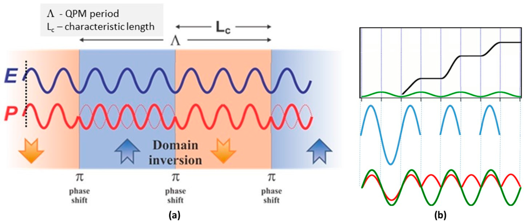
Figure 10.
Diamond structure with inversion symmetry (a) and zinc-blende structure without inversion symmetry (b).
Figure 10.
Diamond structure with inversion symmetry (a) and zinc-blende structure without inversion symmetry (b).

Figure 11.
(a) An optical parametric oscillator (OPO) schematic; (b) signal and idler wavelengths as a function of the QPM period for periodically poled LiNbO3 (PPLN) for = 1.064 μm and T = 25 °C or 200 °C [79]; (c) wavelength as a function of QPM period for the same conversion process in OP-GaP [80] and OP-GaAs [81] (reproduced from [80,81] with some modifications with the permission of J. Appl. Phys.).
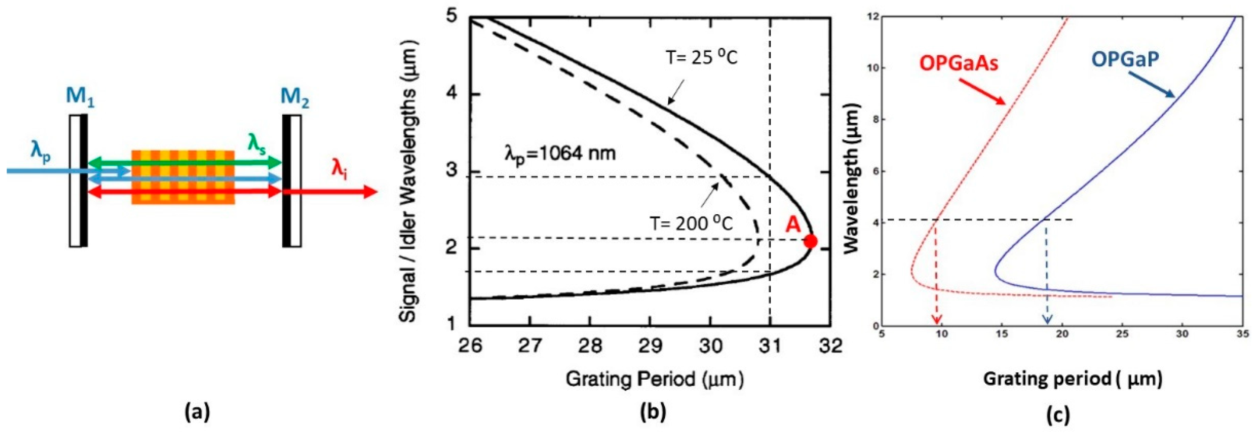
Figure 12.
The hydride vapor phase epitaxial (HVPE) reactors at the Air Force Research Laboratory (WPAFB) used for growth of GaAs, GaP, GaAsP, ZnSe, GaSe, etc.
Figure 12.
The hydride vapor phase epitaxial (HVPE) reactors at the Air Force Research Laboratory (WPAFB) used for growth of GaAs, GaP, GaAsP, ZnSe, GaSe, etc.

Figure 13.
Schematic of the HVPE reactor showing multi-wafer (two sample) growth of GaP in which the parasitic nucleation has been successfully “pushed” behind the substrates [84] (reproduced from [84] with some modifications with the permission of SPIE).

Figure 14.
Reduction of the growth rate with the duration of growth for GaP growth [84] (reproduced from [84] with some modifications with the permission of SPIE).

Figure 15.
Optimizing the growth conditions by observing: (a) the growth rate and the average surface roughness as a function of the substrate temperature; (b) the growth rate as a function of the growth temperature at two different V/III ratios; and (c) the growth rate and the average surface roughness as a function of the supersaturation [84] (reproduced from [84] with some modifications with the permission of SPIE).

Figure 16.
Growth rate as a function of the reciprocal substrate temperature [86,87] (reproduced with some modifications from [86,87] with the permission of J. Cryst, Growth and J. Electrochem. Soc.).

Figure 17.
Nomarski top surface images of quarters of 2-inch wafers taken with image stitching software: (a) Heteroepitaxy of GaP on an (100) GaAs substrate with 4 degree miscut towards [111] B; (b) heteroepitaxy of GaP on an (100) an “on-axis” GaAs substrate; and (c) homoepitaxy of GaP on an (100) “on-axis” GaP substrate [11] (reproduced with some modifications from [11] with the permission of OSA).

Figure 18.
SEM top surface image of: thermally decomposed GaAs surface exposed to H2 only (a) and a protected GaAs surface exposed to AsH3 + H2 (b) during the preheating stage; (c) SEM surface images of GaAs briefly exposed to PH3 + H2 during the preheating stage; (d) AFM image of a small area from Figure 18c [18] (reproduced with some modifications from [18] with the permission of J. Cryst. Growth).

Figure 19.
(a) SEM/energy dispersive X-ray spectroscopy (EDS) analysis of the “damaged” top surface image of the GaAs substrate exposed to PH3 + H2 showing the ternary GaAsP on it; (b) SEM cross sectional image of GaP grown on GaAs where one can see a several micron thick intermediate ternary layer with gradually changing composition according the elemental profile analysis [18] (reproduced with some modifications from [18] with the permission of J. Cryst. Growth).

Figure 20.
(a) Nomarski cross section image of GaP/GaAs; (b) TEM cross section image of the interface shown in (a) that reveals a rough surface interface; (c) high-resolution TEM cross section of the GaP/GaAs interface that shows roughening surfaces, voids and other compositional variations/ distortions near the interface, but not any misfit dislocations (MDs) [18] (reproduced with some modifications from [18] with the permission of J. Cryst. Growth).

Figure 21.
(a) Schematic of a half-patterned (HP) GaAs template; (b) schematic of a HP GaAs template that represents the two mutually perpendicular patterns. The small rectangular images are Nomarski top surface images of the GaP layer after the growth; (c) Nomarski top surface image of the grown GaP of a small area of the substrate that contains the two pattern orientations; (d) top surface and cross sectional images after growth of area A (pattern perpendicular to the major flat) on “on-axis” (upper images) and 4 degree tilted (lower images) HP templates; (e) top surface and cross sectional images after growth of area B (pattern perpendicular to the minor flat) on “on-axis” (upper images) and 4 degree tilted (lower images) HP templates [20] (reproduced with some modifications from [20] with the permission of J. Cryst. Growth).

Figure 22.
(a) Top surface SEM image of a OP-GaAs template fabricated by the molecular beam epitaxy (MBE) assisted polarity inversion technique; (b) cross sectional SEM image of the same template [90] (reproduced from [90] with some modifications with the permission of SPIE).

Figure 23.
SEM top surface images (smaller magnification) of two neighboring domains with opposite crystal polarity of an OP-GaAs template: (a) Before preheating; and (c) after exposing to the non-native precursor (PH3 + H2 flow); (b) SEM image of a small area from (c) at moderate magnification; (d) SEM image of another small area from (c) at larger magnification—the mutual perpendicular orientations of the longitudinal etch pits in the oppositely oriented domains is obvious [18] (reproduced from [18] with some modifications with the permission of J. Cryst. Growth).

Figure 24.
Cross section image of thick HVPE grown OP-GaP on OP-GaAs templates with flat (a) and traditional top surface (b) when typically one of the domains is finished by two (111) facets while the other one is flat finished by only one (100) facet [7] (reproduced from [7] with some modifications with the permission of OSA).
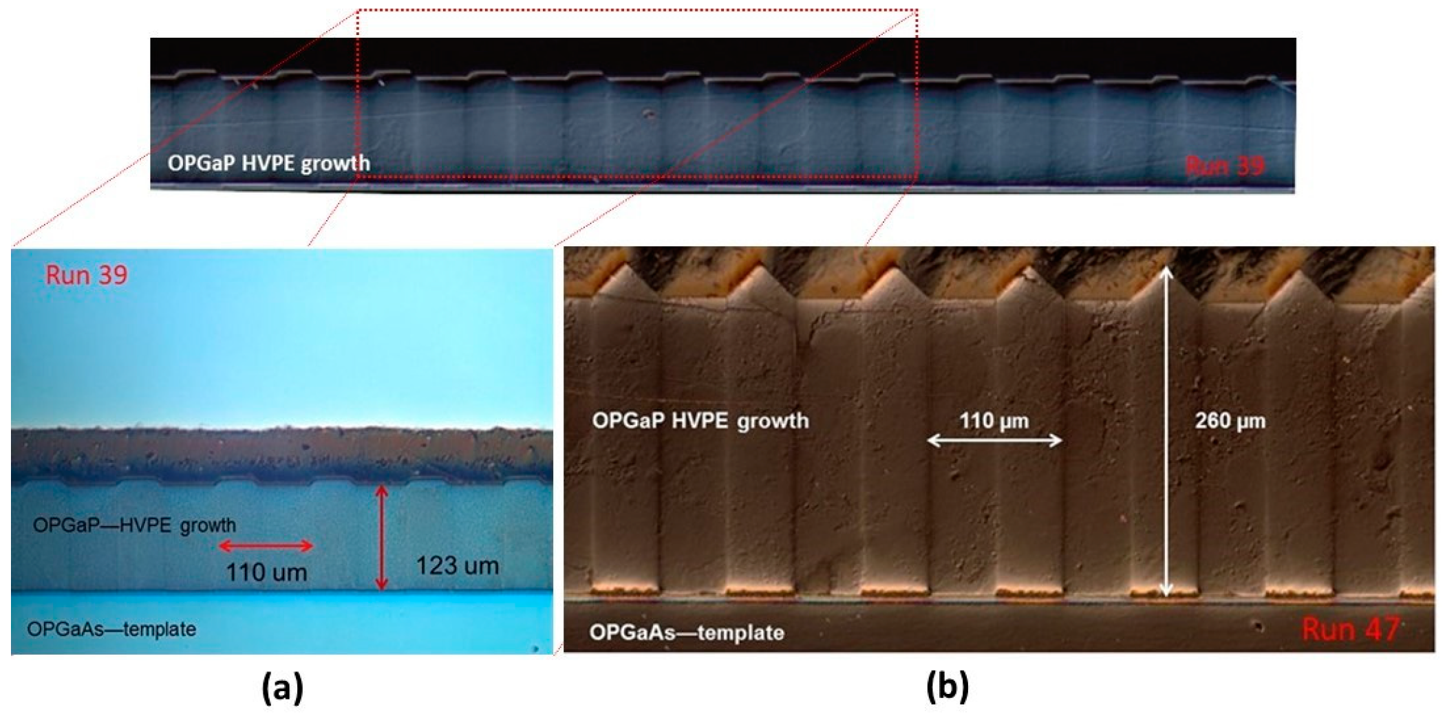
Figure 25.
(a) Cross sectional image of GaAs0.34P0.66 grown on a 4-degree off axis GaP substrate (reproduced with some modifications from [20] with the permission of Crystals); and (b) XRD (004) peak (blue curve) along with a simulation fit (red curve) was used to evaluate crystalline quality of the material and extract the alloy composition values.

Figure 26.
(a) Linear transmission as a function of the wavelength for GaAs, GaP and some of their ternaries; and (b) first nonlinear optical measurements (Z-scan) indicated that the GaAsxP1−x ternaries possess less nonlinearity than the patterning materials, GaP and GaAs [93] (reproduced from [93] with the permission of J. Cryst. Growth).
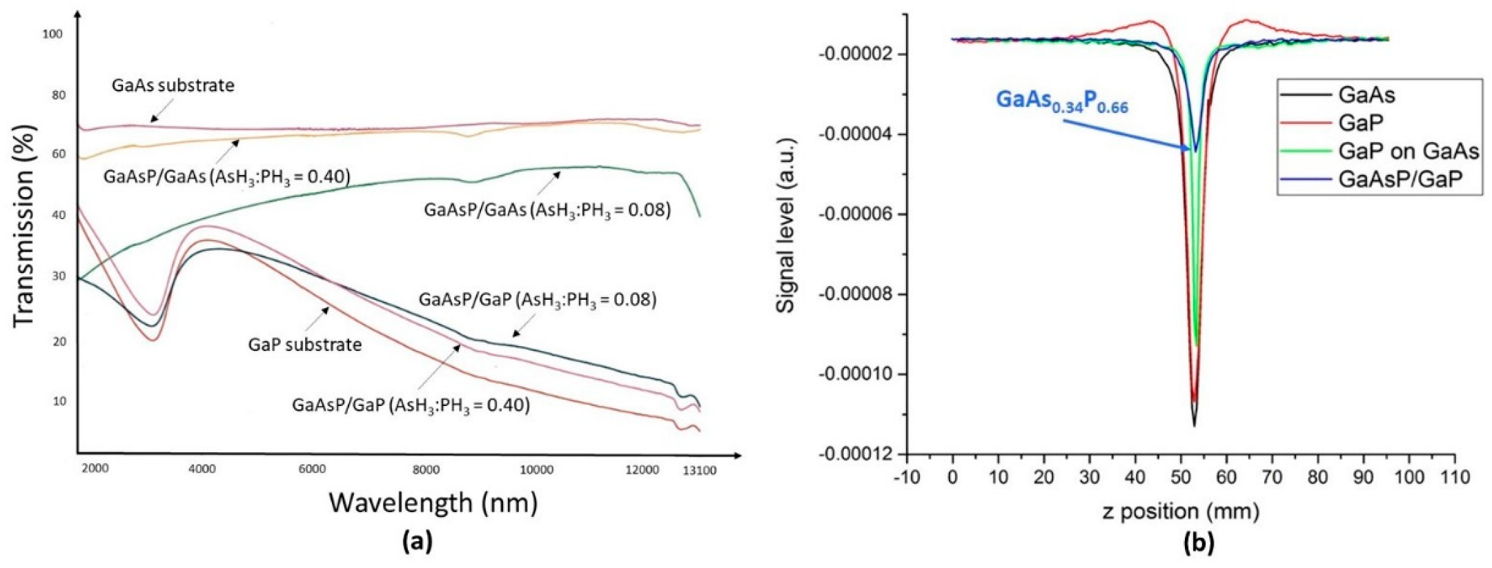
Figure 27.
Thick HVPE growth of OP-GaAsxP1−x ternary on an OP-GaAs template [93] (reproduced with some modifications from [93] with the permission of J. Cryst. Growth).

Figure 28.
(a) SEM cross sectional image of heteroepitaxial grown ZnSe/GaAs; (b) SEM top surface image of heteroepitaxial grown ZnSe/GaAs [96]; (reproduced from [96] with the permission of J. Cryst. Growth).

Figure 29.
(a) SEM cross sectional image of homoepitaxial grown ZnSe/ZnSe; (b) SEM top surface image of heteroepitaxial grown ZnSe/ZnSe; (reproduced from [96] with the permission of J. Cryst. Growth).
Figure 29.
(a) SEM cross sectional image of homoepitaxial grown ZnSe/ZnSe; (b) SEM top surface image of heteroepitaxial grown ZnSe/ZnSe; (reproduced from [96] with the permission of J. Cryst. Growth).

Figure 30.
High-resolution TEM image of the ZnSe/GaAs interface (reproduced from [96] with some modifications with the permission of J. Cryst. Growth).
Figure 30.
High-resolution TEM image of the ZnSe/GaAs interface (reproduced from [96] with some modifications with the permission of J. Cryst. Growth).
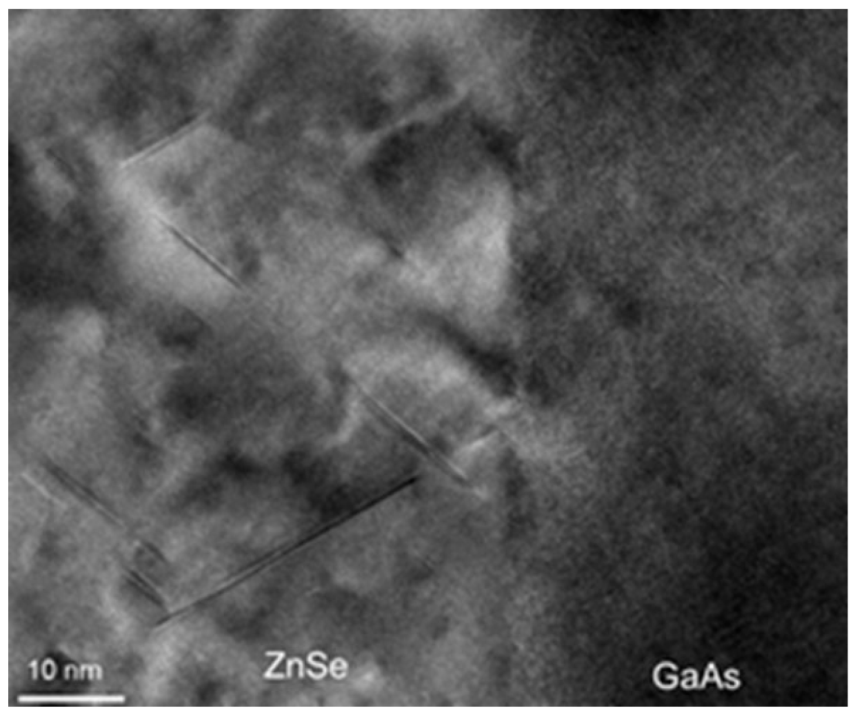
Figure 31.
Cross-section image of one of as-cleaved OP-ZnSe structure grown on OP-GaAs template showing domain propagation up to the surface (reproduced from [96] with some modifications with the permission of J. Cryst. Growth).
Figure 31.
Cross-section image of one of as-cleaved OP-ZnSe structure grown on OP-GaAs template showing domain propagation up to the surface (reproduced from [96] with some modifications with the permission of J. Cryst. Growth).

Figure 32.
Top surface SEM images of GaSe grown on the (a) GaP substrate and (b) GaN/sapphire substrate (reproduced from [93] with some modifications with the permission of J. Cryst. Growth).
Figure 32.
Top surface SEM images of GaSe grown on the (a) GaP substrate and (b) GaN/sapphire substrate (reproduced from [93] with some modifications with the permission of J. Cryst. Growth).

Figure 33.
(a) The SEM images of the GaSe/GaAs show numerous differently sized rectangular pillars oriented with their long side perpendicular to the major wafer flat, i.e., along the [01ī] direction; (b) the EDS analysis on the layer surface shows Ga and Se elements [93] (reproduced with some modifications from [93] with the permission of J. Cryst. Growth).
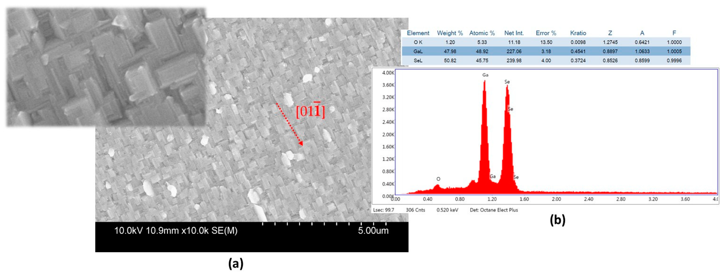
Figure 34.
Theoretical prediction of the critical thickness as a function of the lattice mismatch , for a given example of GaP/GaAs heteroepitaxy [109] (reproduced from [109] with some modifications with the permission of J. Appl. Physics).

Figure 35.
(a) Two samples—one Si substrate with a thin metal organic chemical vapor deposition (MOCVD) GaP layer deposited on it and one GaP substrate; (b) the already bonded pieces from Figure 35a with the thin MOCVD GaP layer between them; (c) the bond after removing by etching the entire Si substrate [28].

Figure 36.
Gross sectional Nomarski optical image of a 470 μm thick HVPE GaP layer deposited on a HP template made using a 350 μm thick (100) GaP with 4 degree off-axis toward [111] B. The lower arrow shows an undesired growth on the back side on the wafer. The small image at left is a SEM image of the top surface of the as-grown layer [20] (partly reproduced with some modifications from [20] with the permission of Crystals).

Figure 37.
(a) Cross sectional Nomarski optical image of a 362 μm deep grooves machined in GaP by a thin diamond blade; (b) laser ablation of deep 30–50 μm wide pattern cuts with 20 μm distance between (Vitec CO2 MX series engraving laser); (c) top surface SEM images of laser ablation made by a femtosecond laser at two different magnifications [29].

Figure 38.
Stages of filling the inorganic half of the QPM matrix with thermo-electret [29].
Figure 38.
Stages of filling the inorganic half of the QPM matrix with thermo-electret [29].


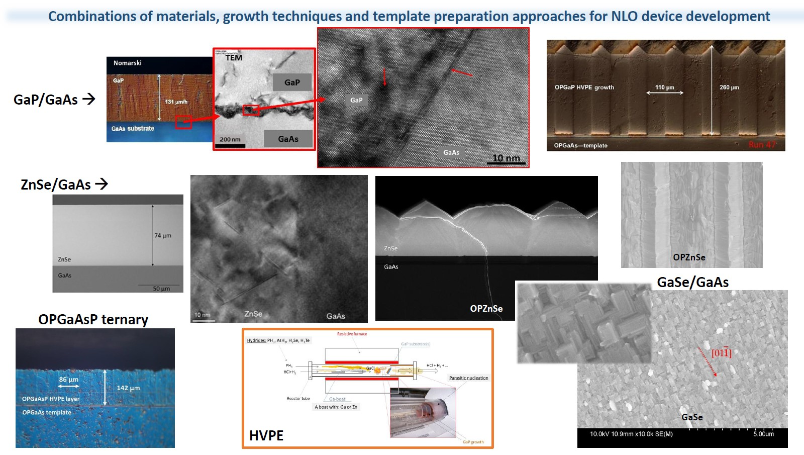
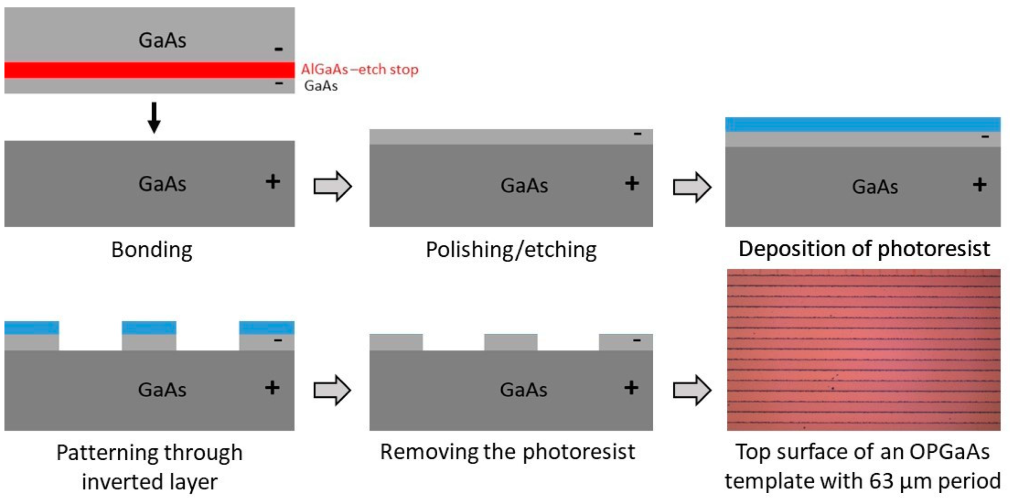
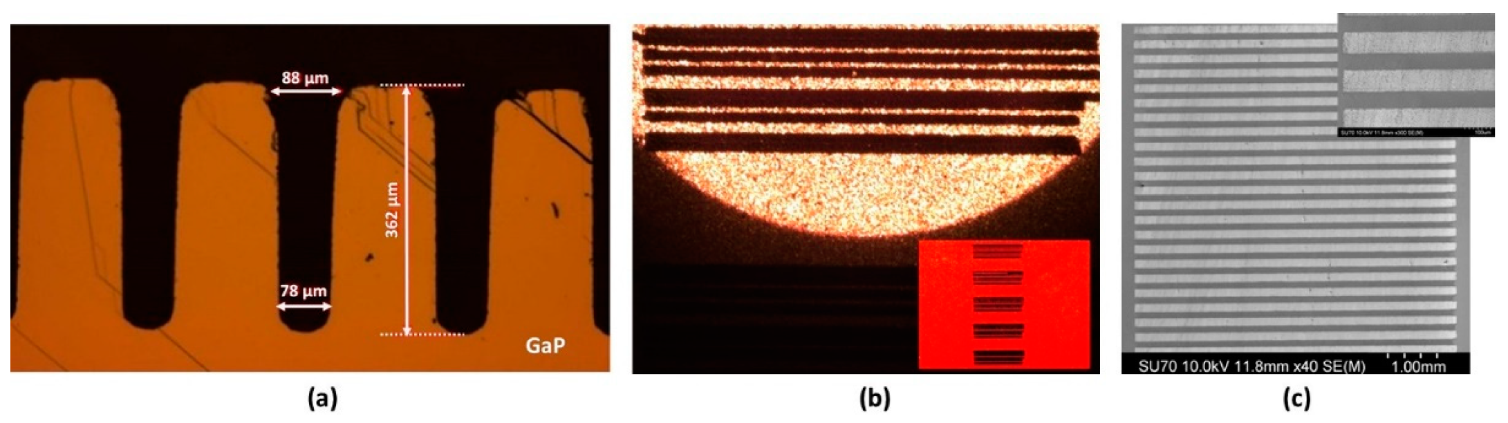
Table 1.
A comparison of properties of GaP and GaAs substrates along with their price.
| Properties | GaAs | GaP |
|---|---|---|
| Transmission window (μm) | 1–16 [88] | 0.5–12 [88] |
| Nonlinear optical coefficient d14 (pm·aV−1; for GaP is for 1.064 μm) | 94 [89] | 71 [89] |
| Index of refraction n (allows wider gratings) | 3.34 [88] | 3.03 [88] |
| Thermal conductivity at 300 K (W·m−1·K−1) | 55 [88] | 110 [88] |
| Thermal expansion coefficient at 300 K (10−6·K−1) | 5.7 [88] | 4.6 [88] |
| Maximum temperature of usage (°C) | 460 [88] | 640 [88] |
| Band gap energy (eV) | 1.42 [88] | 2.26 [88] |
| 2PA coefficient β (cm/G−1·W−1) at 1.06 μm | 28 [9] | 0.02 [11] |
| Etch pits density (EPD; EPD·cm−2; data from wafer suppliers) | 1500–5000 | 8000–100000 |
| Price | GaAs | GaP |
| Price per 2-inch wafer in USD (data from wafer suppliers) | 80–90 | 585–685 |
Table 2.
Performed/planned heteroepitaxial growths: Lattice mismatches, precursor gasses and chemical paths [19,28,92,95].
| Heteroepitaxy | Mismatch | III–Gas | V–Gas (Hydride) | Chemistry Paths |
|---|---|---|---|---|
| GaP/GaAs | –3.574% | HCl | PH3 | 2Ga + 6HCl → 2GaCl3 + 3H2 → GaCl3 + PH3 → GaP + 3HCl |
| GaAsP/GaAs | < –3.574% | HCl | AsH3 + PH3 | 2Ga+ 6HCl → 2GaCl3 + 3H2 → GaCl3 + AsH3 + PH3 → GaAsP + 3HCl |
| GaAsP/GaP | < +3.574% | HCl | AsH3 + PH3 | 2Ga+ 6HCl → 2GaCl3 + 3H2 → GaCl3 + AsH3 + PH3 → GaAsP + 3HCl |
| ZnSe/GaAs | +0.238% | HCl | H2Se | Zn + 2HCl →ZnCl2 + H2 → ZnCl2 + H2Se → ZnSe + 2HCl |
| ZnSe/GaAs | +0.238% | H2 | H2Se | ZnCl2 + H2 → ZnCl2 + H2Se → ZnSe + 2HCl |
| α-GaSe/GaP | –0.607% | HCl | H2Se | 2Ga + 6HCl →2GaCl3 + 3H2 → 2GaCl3 + 2H2Se → 2GaSe + 4HCl + Cl2 |
| α-GaSe/GaAs | –4.181% | HCl | H2Se | 2Ga + 6HCl →2GaCl3 + 3H2 → 2GaCl3 + 2H2Se → 2GaSe + 4HCl + Cl2 |
| β-GaSe/GaN | +17.74% | HCl | H2Se | 2Ga + 6HCl →2GaCl3 + 3H2 → 2GaCl3 + 2H2Se → 2GaSe + 4HCl + Cl2 |
| ZnTe/GaSb | +0.083% | HCl | H2Te | Zn + 2HCl →ZnCl2 + H2 → ZnCl2 + H2Te → ZnTe + 2HCl |
Table 3.
Thermal and linear and nonlinear optical properties of some prospective nonlinear optical (NLO) materials.
Table 3.
Thermal and linear and nonlinear optical properties of some prospective nonlinear optical (NLO) materials.
| Properties | GaAs | GaP | ZnSe | GaSe | ZnTe |
|---|---|---|---|---|---|
| Optical | |||||
| Transmission window (μm) | 1–16 [88] | 0.55–12 [88] | 0.6–18 [88] | 0.6–19 [88] | 0.7–20 [88] |
| Band gap energy (eV) | 1.42 [88] | 2.26 [88] | 2.82 [88] | 2.1 [88] | 2.26 [88] |
| Index of refraction n | 3.34 [88] | 3.03 [88] | 2.67 [88] | 2.93 [88] | 3.56 [88] |
| NLO coefficient d14 at 1.064 μm (pm·V−1) | 94 [89] | 71 [89] | 27 [89] | 86 [89] | 90 [89] |
| 2PA coefficient (cm/G−1·W−1) at 1.06 μm | 28 [9] | 0.02 [11] | 5.5 [89] | 6 [89] | 4.5 [89] |
| Thermal | |||||
| Thermal conductivity at 300 K (W·m−1·K−1) | 55 [88] | 110 [88] | 18 [88] | 5.0 [88] | 10.8 [88] |
| Thermal expansion coeff. at 300 K (10−6·K−1) | 5.7 [88] | 4.6 [88] | 7.1 [88] | 8.9 [88] | 8.19 [88] |
© 2019 by the authors. Licensee MDPI, Basel, Switzerland. This article is an open access article distributed under the terms and conditions of the Creative Commons Attribution (CC BY) license (http://creativecommons.org/licenses/by/4.0/).
Share and Cite
MDPI and ACS Style
Tassev, V.L.; Vangala, S.R. Thick Hydride Vapor Phase Heteroepitaxy: A Novel Approach to Growth of Nonlinear Optical Materials. Crystals 2019, 9, 393. https://doi.org/10.3390/cryst9080393
AMA Style
Tassev VL, Vangala SR. Thick Hydride Vapor Phase Heteroepitaxy: A Novel Approach to Growth of Nonlinear Optical Materials. Crystals. 2019; 9(8):393. https://doi.org/10.3390/cryst9080393
Chicago/Turabian StyleTassev, Vladimir L., and Shivashankar R. Vangala. 2019. "Thick Hydride Vapor Phase Heteroepitaxy: A Novel Approach to Growth of Nonlinear Optical Materials" Crystals 9, no. 8: 393. https://doi.org/10.3390/cryst9080393
Note that from the first issue of 2016, this journal uses article numbers instead of page numbers. See further details here.