Integrated Photonic Devices Incorporating Low-Loss Fluorinated Polymer Materials


Abstract
: Low-loss polymer materials incorporating fluorinated compounds have been utilized for the investigation of various functional optical devices useful for optical communication and optical sensor systems. Since reliability issues concerning the polymer device have been resolved, polymeric waveguide devices have been gradually adopted for commercial application systems. The two most successfully commercialized polymeric integrated optic devices, variable optical attenuators and digital optical switches, are reviewed in this paper. Utilizing unique properties of optical polymers which are not available in other optical materials, novel polymeric optical devices are proposed including widely tunable external cavity lasers and integrated optical current sensors.1. Introduction
Research on polymeric integrated optical devices has spanned over two decades. Originally this research was initiated by the material scientists who proposed conjugated organic molecules consisting of electron doner-acceptor molecules leading to permanent electric dipoles. Through the poling of the dipoles doped in the polymer, one can introduce significant nonlinear optical effects which compete with those of the renowned inorganic crystal, lithium niobate. The explosive expansion of Internet traffic has created strong demand for low-cost high-speed optical modulators which can be realized by using electro-optic (EO) polymers [1]. Polymeric EO modulators draws attention by its merits of large modulation bandwidth derived from the small dispersion of dielectric constant over a wide frequency range, covering millimeter to optical waves. Consequently, the lower velocity mismatch of the two waves enables superior modulation bandwidth in polymer modulators [2]. In spite of the demonstration of 100 GHz signal modulation, EO polymer modulator have experienced difficulties to address several reliability issues, which includes the relaxation of poled order, photo-oxidation of chromophore exposed to strong optical field, and drift of the DC bias point in Mach-Zehnder interferometric modulators [3]. Recently, much effort has been devoted to improve the stability of EO polymer materials, and the modulator device have exhibited improved thermal and photostability in a hermatic package [4,5].
As optical communication systems evolve toward more sophisticated configurations, such as wavelength division multiplexing, demands on various functional waveguide devices have been increasing in which various optical signal processing devices become important. To meet with the demand for various functional devices, polymer device research based on low-loss polymers has emerged. However, due to the vibrational overtone absorption of the C–H bond, which could be reduced by substituting hydrogen with fluorine, polymer waveguides had higher propagation loss compared to silica waveguide devices, which had been widely adopted for passive optical devices such as wavelength multiplexers and optical power splitters [6,7]. In spite of the larger propagation loss, polymer waveguide devices have the merit of high thermo-optic (TO) effects along with good thermal confinement [8]. Therefore, large index tuning is capable in polymer devices so as to enable novel device structures such as the digital optical switches (DOS), for which 10 times larger refractive index change is required than the other interferometric switches [9]. In DOS, precise input power control is not necessary for the switching because the device only needs to have refractive index change higher than a threshold value, as for a digital logic device. Especially, in the case of array devices such as NxN optical switches, the digital characteristics are useful for increasing fabrication tolerances so as to improve production yield. The strong TO effect is also very attractive for novel variable optical attenuators (VOA) [10,11]. Compared to Mach-Zehnder interferometric VOAs made from silica waveguides, polymer VOAs rely on the large index TO index change in order to radiate the guided light out of the channel waveguide.
In the early stage of TO polymer device development, skepticism over the reliability of polymer devices was widespread due to difficult experiences during the early EO polymer device development during which people observed degradation of the EO effect and photo-oxidation of the chromophores [12]. Though passive low-loss polymers do not contain any unstable molecules, engineers were reluctant to accept polymer devices in their optical communication systems requiring stable operation over 20 years. To resolve this skepticism on polymer devices, it was necessary to accumulate sufficient reliability data in accordance with the Telcordia reliability assurance guidelines [13]. Among the many requirements, the damp heat test (85 °C/85% RH) and temperature cycling test were the most difficult to pass for polymer devices. Weak adhesion of the fluorinated polymer materials on the surface of inorganic substrates often caused film lift-off when devices were exposed to humidity at elevated temperatures. Through the improvement of chemical properties of polymer materials and the investigation of surface adhesion chemistry, the stability of polymer devices has been greatly improved, and finally it has passed all of the reliability assurance requirements [11].
TO polymer devices nowadays have been installed in various optical communication systems. VOAs made of polymers have faced strong competition from MEMS devices. However, as optical communication evolves toward large bandwidth capacity using many wavelengths, low-power, small-foot-print array devices based on polymer waveguides, they will gradually dominate the commercial market. Polymeric optical switches have been competing with fiber-optic switches and MEMS devices. In terms of optical signal crosstalk, because of the limit of the adiabatic transition in asymmetric Y-branch waveguides, polymer switches have struggled to compete. To overcome this limitation, a VOA section was cascaded after the switch on a single chip so as to reduce the remaining crosstalk light [14]. Since the polymer DOS overcame the crosstalk issue, the devices have been widely deployed for optical backbone network used for wireless communication.
Along with the commercial penetration of the polymer VOAs and DOSs, there has been significant progress on the development of novel polymer waveguide devices which further highlights the unique properties of polymer materials. In this paper, starting from an introduction to the current status of commercialized polymer devices, recent achievements of our group on novel polymer devices will be reviewed, including tunable lasers using TO polymer Bragg reflector and integrated optical devices for optical current sensors. External cavity tunable laser has a simple tuning mechanism and wide tuning range, so has recently been adopted for passive optical network applications. In the optical current sensor, various functional optical devices are required to provide a reflection interferometer for measuring minute changes of polarization angle. Optical waveguide technology based on polymers play a major role in integrating all of the optical devices on a single chip in order to facilitate optical sensor fabrication and reduce production expenses, which are critical for expansion of the optical current sensor market, and to open new application areas.
2. Polymer Waveguide Devices Based on Thermo-Optic Effect
2.1. Fluorinated Polymers with Low Absorption Loss
Optical polymer materials have been intensively developed to meet the requirements for high performance thermo-optic devices. The material properties required for optical devices are low absorption loss, controllable optical refractive index, low optical birefringence, and long-term environmental stability. Considerable efforts have been devoted to reduce the near-IR optical loss, which is principally introduced by the vibrational absorption of C–H bonds in the polymer chain. By replacing the C–H bond with the C–F bond, one can reduce the optical loss and increase the thermal stability due to the heavy mass of fluorine and the higher bond strength of C–F bond. There have been various approaches to synthesizing low-loss optical polymers based on acrylates [15], polyimides [16], polyarylene ethers [17,18], and perfluorocyclobutane [19]. Among them, fluorinated UV-curable acrylates have been most actively investigated because of their convenient low temperature processing with UV curing. Therefore, our research has been focused on the development of highly fluorinated UV-curable acrylate polymers.
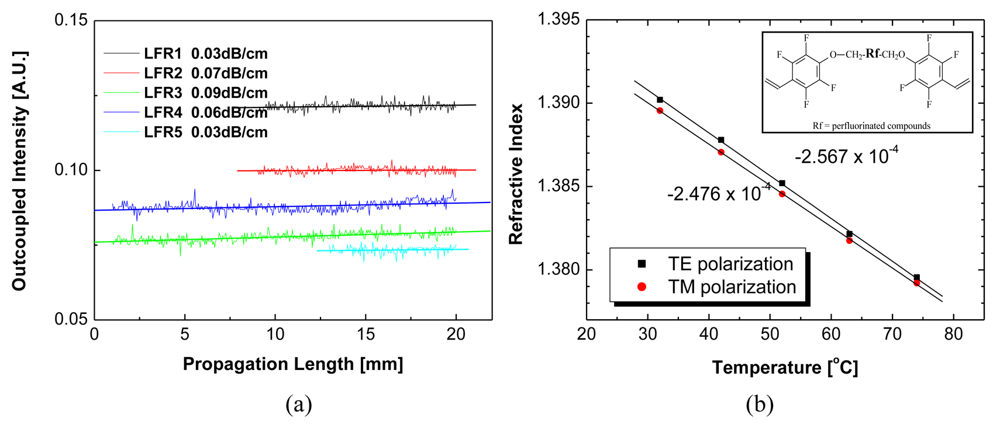
The first version of fluorinated low loss polymer was the ZPU series with a propagation loss of 0.2 dB/cm, in a planar waveguide structure. The loss has been reduced by increasing the fraction of fluorinated material and lowering the glass transition temperature to reduce the stress on the cured polymer film. The recently developed low-loss polymer is the LFR series which has a minimum absorption loss of 1,550 nm and low birefringence in a crosslinked thin film. The basic chemical structure of the LFR is illustrated on the inset of Figure 1. To investigate the propagation loss of the LFR series polymer, the liquid immersion loss measurement technique was used [20]. By fabricating a planar waveguide on a silicon substrate with two layers of LFR polymers, we measured the propagation loss of the material by the liquid immersion prism coupling technique. Because the polymer had very low loss, it was hard to obtain clear data with this measurement. After repeated measurements, as shown in Figure 1(a), a conclusion was drawn that the waveguide has a propagation loss of less than 0.1 dB/cm at 1,550 nm. The TO effect of the polymer material was investigated to find the tuning range of refractive index obtainable by electrical heating. Figure 1(b) shows the refractive index of the polymer material as a function of temperature, which corresponds to a TO coefficient of −2.567 × 10⁻⁴ /°C and −2.476 × 10⁻⁴ /°C for TE and TM polarizations, respectively. From the measured TO coefficient, for the case of a tunable laser, to obtain wavelength tuning for 32 channels with 0.8 nm spacing, the temperature change needed at the waveguide core was estimated to be 87 °C.
2.2. Polymer Waveguide Variable Optical Attenuators
Wavelength division multiplexed optical communications require various kinds of functional optical devices including wavelength multiplexers, optical amplifiers, optical switches, and variable optical attenuators (VOA). By virtue of the large TO effect of polymers, a novel polymer VOA design has been proposed [10,11]. A schematic diagram of the proposed VOA structure is shown in Figure 2(a). The multi-mode waveguide section in the middle of the device plays a key role in the device operation. The heating electrode covers the multi-mode waveguide section at an angle of α to introduce an index change by the TO effect. The operating principle of the VOA is explained in terms of the mode coupling and filtering. According to beam propagation method (BPM) simulation, adiabatic fundamental mode propagation is observed when there is no index perturbation for a taper angle of less than 0.6°. When a voltage is applied across the heating electrode, the refractive index underneath the heater is lowered so that the guided mode couples to higher order modes along with a partial reflection by an angle of 2α. These excited higher order modes are filtered out as they propagate through the output tapered single mode waveguide.
The single mode waveguide at the input and output section is designed to have 7 × 7 μm2 rectangular cross-section with a core-cladding index contrast of 0.34%. The upper cladding has a lower refractive index than the lower cladding in order to reduce the required upper cladding thickness and enhance the heating efficiency on the core. Based on 3D BPM analysis, it is confirmed that over 30-dB attenuation is obtainable for a temperature difference of 60 °C.
Typical attenuation characteristics of a fabricated VOA at 1,310 and 1,550 nm are shown in Figure 2(b). The length of the fabricated device was 1 cm, and the fiber-to-fiber insertion loss of the device without applied voltage was less than 1 dB and 0.7 dB for 1,550 nm and 1,300 nm, respectively. The propagation loss and the coupling loss measured by the cutback method were estimated to be about 0.5 dB/cm and 0.15 dB/facet, respectively. The propagation loss measured by cut-back was higher than that of the slab waveguide measured by the immersion technique, which could be caused by some material imperfections and side wall roughness. For the shorter wavelength, a higher attenuation was obtained for the same applied voltage, because the shorter wavelength experiences the larger phase change in the propagation and more coupling into the higher order mode. The electrical power to obtain 30-dB attenuation was 29 mW and 24 mW for 1,550 nm and 1,300 nm, respectively.
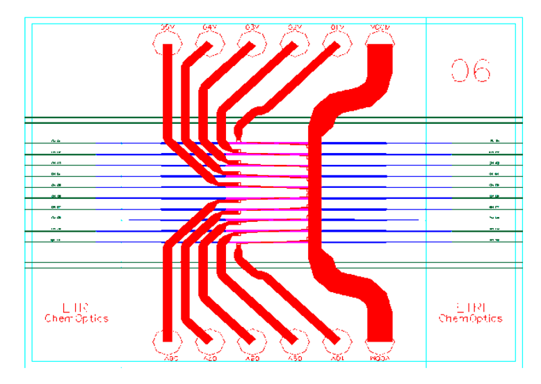
As the number of channels in WDM optical communications is increasing beyond 40 channels, the number of optical components is increasing so that an array device is desired to reduce the complexity of the optical signal processing board. Compared to MEMS devices, polymer VOAs based on waveguide technology, are very convenient for increasing the number of channels for array devices. In addition, polymer VOAs have very low operating power, which is important for array devices consuming a large amount of electrical power. Figure 3 shows the photomask drawing of the 10-channel VOA array device, which is currently used for a 40-channel reconfigurable optical add-drop multiplexing (ROADM) WDM system.
2.3. Polymer Waveguide Digital Optical Switches
Optical switches have received great attention as an essential component in optical networks for optical cross-connects, optical add-drop multiplexing, and network protection. Polymer waveguide TO switches have been investigated for some time due to the potential of integrating multi-functional devices and cost effective mass production [21,22]. The large TO coefficient of the polymer as well as low thermal conductivity, enables highly efficient TO index modulation. Consequently, digital optical switches (DOSs) based on the mode sorting effect were proposed, which requires an order of magnitude higher refractive index change for the switching compared to an interference type switch [23]. DOS has many advantages over interference type switches such as large fabrication tolerance, modest control of the drive electrical power, and low dependence on the signal wavelength. However, from a conventional DOS, it is hard to reduce the crosstalk below −30 dB, which is often critical for practical applications.
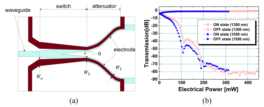
To improve the crosstalk of the conventional DOS, several methods have been proposed including a cascaded DOS switch, in which the crosstalk was suppressed by incorporating additional DOS switches to achieve a crosstalk of less than −60 dB. However the insertion loss was relatively high due to the long device length [24]. VOA integrated DOSs were demonstrated to enhance the crosstalk by attenuating the remained light in the switch-off branch [14,25,26]. The device consists of a conventional Y-branch waveguide and heating electrodes on top of the waveguide pattern as shown in Figure 4(a). It can be divided into two sections, the switch section and the attenuator section. The switching section is designed to have optimum adiabatic mode evolution for low crosstalk. Based on BPM simulation, the waveguide size is determined to be 7 × 7 μm2 for single mode operation at 1,550 nm with an index contrast of 0.34%. The branch angle is determined to be 0.2 degrees for optimum switch operation. When electrical power is applied to one of the heating electrodes, the refractive index of the waveguide branch under the heater is decreased by the thermo-optic effect of the polymer. As a result, the guided mode evolves into the other branch where the refractive index is not decreased.
After the switch section, an integrated attenuator is formed by extending the switch electrodes to cover the curved waveguides after the Y-branch. When one of the branching waveguides is heated, the signal switches to the other branch. However, a small amount of light remains at the heated branch, and causes the crosstalk. In the proposed device, the heater on the attenuator section reduces the refractive index of the curved output waveguide. This remaining light causing the crosstalk is barely guided through the curved output waveguide so that the crosstalk is greatly reduced. The heating electrode used for the switch and the attenuator are connected and controlled by a single current source.
The device was evaluated for both 1,300 and 1,550 nm wavelengths. Fiber-to-fiber insertion losses of 0.8 and 1.1 dB were obtained for 1,300 and 1,550 nm, respectively. Polarization dependent loss was less than 0.1 dB for 1,550 nm. As a function of the applied electrical power, the transmissions of the two output ports were measured as shown in Figure 4(b). It was clearly shown that the response was the product of the DOS switch and the waveguide attenuator characteristics. The periodic fluctuation observed from the off-state branch was an inherent characteristic of the DOS switch due to an incomplete adiabatic transition. An extremely low crosstalk of less than −70 dB was achieved for both wavelengths, and the device showed good digital switching response with no additional loss. The switching power needed to obtain the minimum crosstalk for both wavelengths was about 200 mW.
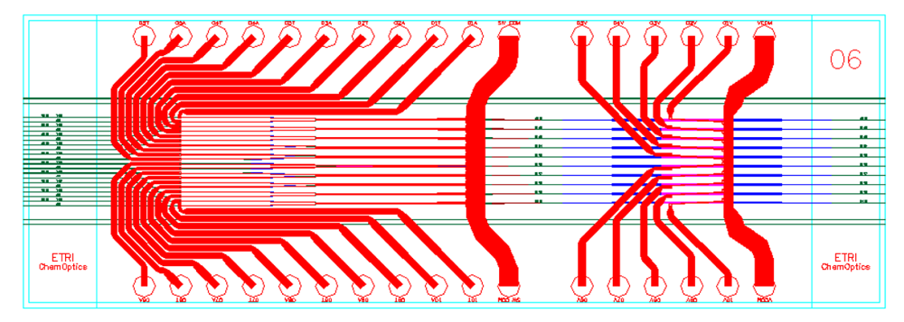
In ROADMs of WDM optical communications, optical switches are always used in a cascaded configuration with VOAs. Hence, there is strong demand to integrate the two components on a single chip. Polymer waveguide device could provide the most appropriate solution for this request because the two devices have been successfully demonstrated using polymers with low driving power. Figure 5 shows the photomask drawing of the integrated VOA-DOSs for 10 channels, which is currently under development.
2.4. Reliability of Polymeric Optical Waveguide Devices
According to the Telcordia reliability assurance requirements for passive optical components GR-1221-core, optical components needed to pass a series of tests to show their mechanical integrity and endurance [13]. For polymeric devices, mechanical integrity is relatively easy to prove since solid-state polymer components do not have any moving parts. Following the standard procedures described in GR-1221-core, we performed a mechanical shock test, a variable frequency vibration test, and a thermal shock test. For each test, 11 VOA samples are prepared as the minimum number of samples for statistical analysis. The change of insertion loss was negligible so that the polymer VOA device passed all the tests of mechanical integrity.
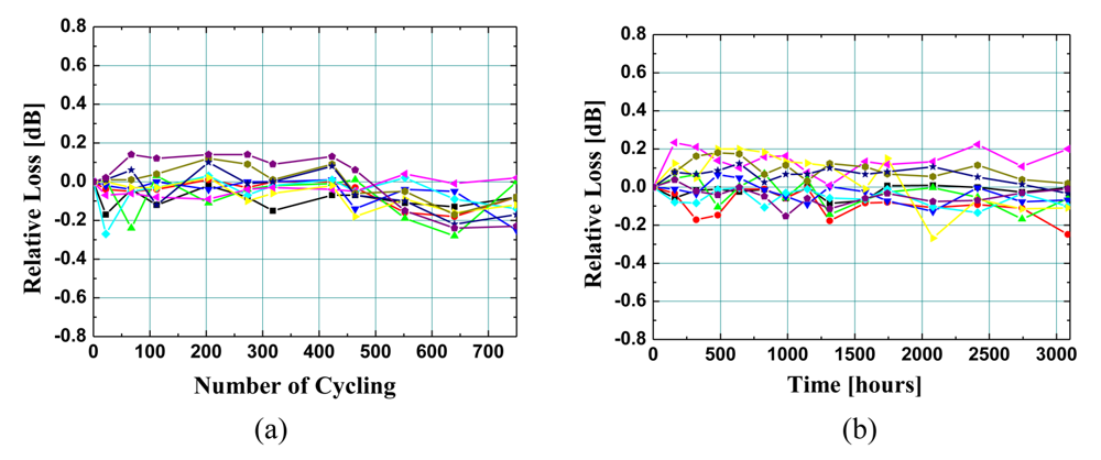
The temperature cycling test was performed based on the procedures stated in MIL-STD-883, method 1010 of Telcordia requirements. The temperature of the oven is cycled from −40 °C to 85 °C in 7 hours and 20 min. The fluctuation in the loss variation was less than 0.3 dB. Figure 6(a) shows the variation of the insertion loss measured from 11 VOA samples for more than 700 cycles (500 cycles required by Telcordia). Successful test results were obtained with a loss change less than ±0.2 dB.
The damp heat test was also performed for 11 VOA samples. To pass the test, the change of insertion loss has to be less than 0.5 dB after 2,000 hours of storage at 85 °C with 85% relative humidity (RH) for uncontrolled environment applications. The data measured during the damp heat test are shown in Figure 6(b). Less than ±0.2 dB of loss fluctuation was observed for the entire test period. Before the damp heat test, as an accelerated endurance test, we also performed a conventional pressure cooker test (PCT) at 120 °C, 2 atm with 100%RH, which is about 100 times more effective than the 85 °C, 85%RH. The device also passed the PCT test over 30 hours suggesting that it could withstand 3,000 hours of 85 °C, 85%RH environment test. There was no adhesion problem observed at the interfaces of polymer-silicon and polymer-heater during the tests. In addition to these passive loss measurements, the attenuation characteristics were checked after each reliability test. There was no significant effect on the VOA performance during the various reliability tests.
3. Tunable Wavelength Lasers Incorporating Polymer Waveguide Bragg Reflectors
3.1. Bragg Reflectors Based on Low-Loss Polymer Materials
In order to manipulate optical signals consisting of multiple carrier wavelengths transmitted through a single optical fiber, an optical device to select a certain desired wavelength is necessary. Bragg reflection gratings fabricated in single mode optical waveguides have very narrow reflection or transmission bandwidths for selecting a single wavelength at a channel spacing of 0.8 nm. Bragg reflectors can be readily inscribed in silica optical fibers by using the high power pulsed laser, though the silica Bragg reflector does not provide sufficient tuning capability. On the contrary, due to the large TO effect of optical polymers, one can change the reflection wavelength of the polymeric Bragg reflector over a wide range by using a thin film heater.
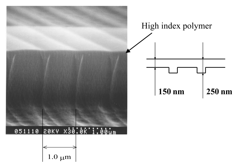
In the first demonstration of the polymer Bragg reflector, a surface relief grating was fabricated incorporating a high refractive index material, Resole [27,28]. The large index contrast between the core polymer and Resole introduces sufficient amount of effective index contrast at a thickness modulation of 100 nm. An SEM photograph of the surface relief Bragg gratings formed on top of a polymer waveguide is shown in Figure 7. The core polymer used in this device was FPAE (fluorinated polyaniline ether) synthesized by our group [17], and the cladding was PFCB (perfluorocyclobutyl) produced by Dow Corning, Co. [19]. A 10 nm tuning range was demonstrated as an initial experimental result. A tunable Bragg reflector was also demonstrated based on photo-chemical refractive index change induced by UV exposure [29]. In this way, the uniformity of grating was further enhanced so as to provide band rejection efficiency over 50 dB.
3.2. External Cavity Tunable Lasers
There have been various approaches to the demonstration of tunable lasers, especially for WDM applications. Wide tuning range was accomplished by incorporating an acousto-optic tunable filter in lithium niobate [30], a coupled ring resonator in a silica waveguide [31], an additive Vernier effect by relative tuning of two modulated gratings [32], and a silicon waveguide grating router with a thermo-optic phase shifter [33]. In addition to wavelength tuning, to prevent channel crosstalk during wavelength switching, a tunable laser integrated with a variable optical attenuator was also demonstrated [34]. In order to obtain a cost-effective solution, a polymeric waveguide Bragg reflector with a thermo-optic (TO) tuning capability was incorporated for providing external feedback of a specified wavelength into a superluminescent diode (SLD) with a broad gain spectrum [35]. A polymer waveguide has the merits of a large TO effect as well as high efficiency for heat insulation, resulting in large refractive index tuning for small power consumption. Hence, the direct tuning of a Bragg reflector, requiring a large index change, become viable in a polymer waveguide just by applying heat onto a simple grating structure.
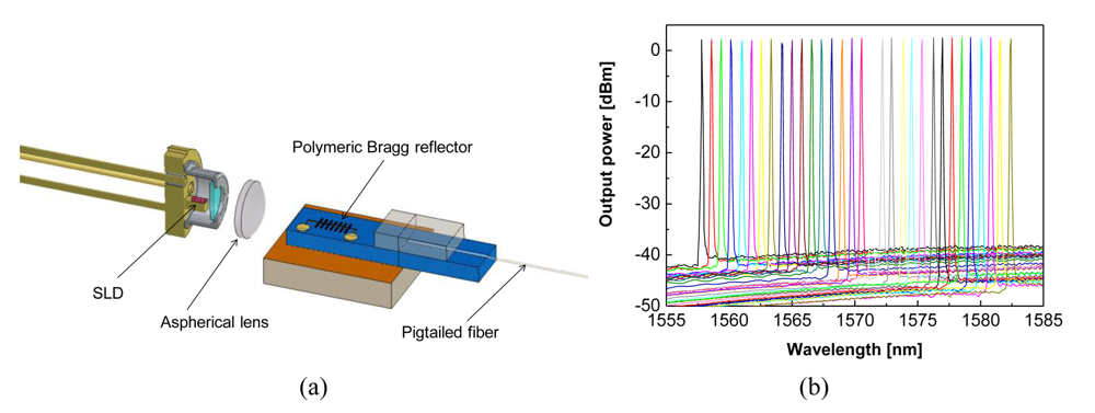
The tunable laser, as depicted in Figure 8, consists of a polymer waveguide device integrated with a Bragg reflector, a SLD light source, and an aspherical microlens between the two components. TO-can type hermetically packaged SLD was used. Due to improved stability, the polymer waveguide device could be operated in air with no need for costly hermetic packaging. The source light emitting from a mode size converted waveguide was coupled to a polymer waveguide through an aspherical microlens. By applying a current to the integrated heater of the polymer device, the reflection wavelength of the Bragg reflector was controlled, which determined the lasing frequency of the tunable laser.
Wavelength tuning characteristics were measured by applying electrical heating power to the micro-heater on the device. As shown in Figure 8(b), the output wavelength was tuned over the 32 wavelength channels with a channel spacing of 0.8 nm by applying an electrical power of 150 mW for maximum tuning. For demonstrating continuous tuning of the lasing wavelength, the device was tuned with a step size of 0.1 nm by the precise control of the heating power. The output power of the tunable laser was set to 3 dBm, and the power fluctuation during the tuning was negligible. The linewidth of the lasing spectrum was measured to be 0.1 nm at 20 dB from the peak.
3.3. Strain-Tunable Lasers with Flexible Bragg Gratings
Compared to inorganic optical devices, polymer waveguide have many unique and useful properties including its large elasticity. Polymers can be elongated by over 10% before they reach their elastic limit, whereas less than 1% of elongation is available in silica fiber [36]. Hence, a significant enhancement of the tuning capability could be achieved if one could produce a Bragg reflecting waveguide on a flexible polymer substrate, as demonstrated in our preliminary experiment [37]. The flexible Bragg reflector could be incorporated with a superluminescent laser diode (SLD) in order to demonstrate a widely tunable compact laser.
The polymeric Bragg reflector consists of a rib waveguide structure and a grating located at the interface between the core and cladding polymers. To impose a strain along the light propagation direction and change the effective grating period, an appropriate fixture to hold the flexible sample is prepared. The SLD has a mirror on one side and the Bragg reflector is connected to the other side, in order to provide the feedback of the wavelength to be lasered. As the grating period changes due to the imposed strain, the reflection wavelength is shifted to shorter or longer wavelengths. Polymer materials generally have a negligible strain-optic effect and, consequently, the tuning wavelength is predominantly determined by mechanical elongation [38].
The flexibility of polymer waveguides is achieved by fabricating them on a flexible substrate. The refractive indices of the polymer materials chosen for the device design are 1.455 and 1.430 for the core and cladding layers, respectively. The large index contrast of the waveguide is favorable for increasing the reflectivity in a compact device with a limited grating length. Even in the case of a large contrast, a single mode waveguide with a mode size comparable to that of single mode fiber is obtainable by adopting an oversized rib structure [39]. Calculation of the effective index indicates single mode operation for a waveguide core of 4 × 6 μm2 and a rib height of 1.6 μm.
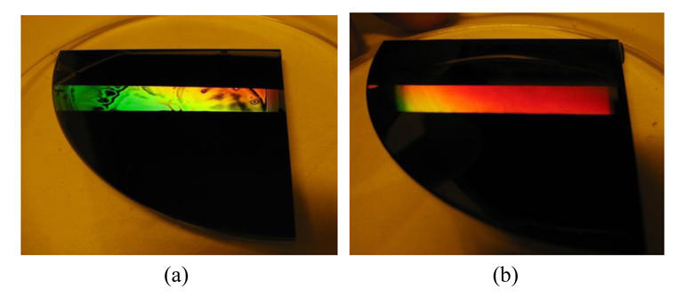
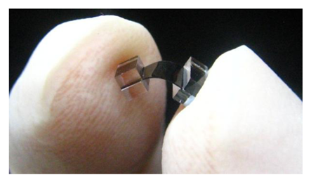
The direct fabrication of polymer waveguide devices on top of a flexible polymer substrate is rather complicated because the plastic substrate is easily bent during the baking and has poor heat transfer. Hence, we adopted a post lift-off process based on the selective adhesion property of SU-8 material [40]. Post-lift off of the flexible layer, after it is fabricated on a hard silicon substrate, facilitates the fabrication of the flexible device. The device was fabricated on a silicon wafer coated with a patterned Au/Cr layer for selective lift-off. The flexible substrate consisted of SU-8/NOA61/SU-8 layers with a total thickness of about 100 μm. To provide good flexibility, NOA61 is used to form the thickest layer of flexible substrate instead of using the stiff SU-8 single layer. On the flexible substrate, the waveguide layer was formed by spin coating and UV-curing two ZPU polymers as the core and claddings. A 2-mm long Bragg grating was fabricated on top of the lower cladding layer by laser interferometry at 442-nm (He-Cd laser) and subsequent plasma etching. Subsequently, by over coating the core material, a periodic modulation of the core thickness was achieved to form the Bragg grating. For improving grating uniformity, an underlying black matrix polymer was used to prevent any undesired interference patterns [38]. Figure 9 compares the uniformity for gratings with and without the black matrix absorption layer. It is clearly observed that the fringe pattern disappeared for the sample with the black matrix. Figure 10 shows the 5-mm long flexible Bragg grating waveguide device with glass blocks attached for fiber pigtailing.
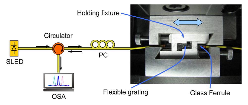
For the wavelength tuning experiment, the sample was carefully attached to the motorized micro-translation stage, as shown in the photograph in Figure 11. In this setup, one can impose both tensile and compressive strain along the longitudinal direction, in order to change the actual period of the Bragg grating. By connecting the tunable Bragg reflector to an SLD with a mirror at one end, a tunable laser was constructed, where the output light was directed toward the other end of the Bragg reflector [41]. The SLD has a center wavelength of 1,535 nm, a 3-dB bandwidth of 50 nm, and a slope efficiency of 0.105 A/W at 25 °C. The output spectrum of the laser exhibited initial lasing at 1,536.9 nm with a side mode suppression ratio of 35 dB. The spectrum measured by a spectrum analyzer with a resolution of 0.05 nm exhibited a 20-dB bandwidth of 0.12 nm and 3-dB bandwidth of 0.05 nm, which was hard to measure due to the resolution limit of the optical spectrum analyzer. The output power of the laser was −3.5 dBm, but could be improved by polishing the end facet to reduce pigtail loss.
The tuning characteristics of the laser were measured by the same procedure as that used for reflection spectrum tuning. For a tuning range of 10 nm, the spectra were measured with a maximum resolution of 0.05 nm as shown in Figure 12(a). The output optical power was −10 dBm in this sample, due to the rough end facet as diced. There was no significant change of the lasing spectrum during the tuning process. The tuning range was extended to 80 nm for a total applied strain of 57,143 με (5.7%), as shown in Figure 12(b). Throughout the entire tuning range, the output power fluctuation was less than 0.5 dB. No abrupt change of the lasing wavelength was observed when the strain crossed over the tension-compression border.
4. Integrated Photonic Current Sensors with Polarization Controlling Waveguide Devices
4.1. Polarization Controlling Polymeric Optical Waveguide Devices
Optical waveguide devices used for optical communication systems usually require polarization independent characteristics because the light signal transmitted through single mode fiber generally have randomly polarized state. Hence, the material used for the device is preferred to have low optical birefringence. On the other hand, for the purpose of fabricating polarization controlling devices (PCDs), such as polarization splitters, polarizers, and polarization converters, polymers with large birefringence are required. Large birefringence induced by the electric field poling of chromophore-doped polymers was utilized for the demonstration of polymer waveguide PCDs [42-44]. Polyimide materials developed for electronic devices were also adopted for PCD fabrication because they exhibit large optical birefringence when cured in the form of a thin film [45,46]. However, owing to the large optical absorption of the birefringent polymers used in these experiments, the insertion loss was too high to provide low-loss devices acceptable for practical applications.
PCDs have recently received much attention due to the evolution of optical communication systems in order to respond to the growing demand of data traffic expansion. In recent 100-Gb/s coherent optical communication systems, polarization division multiplexing has been adopted to increase the transmission capacity [47,48]. In such systems, it is highly desirable to employ low-cost compact integrated optic PCDs that can be integrated with other functional optical devices such as optical switches, optical power couplers, and tunable wavelength filters that have been successfully demonstrated with polymer waveguides.
The birefringence of an optical polymer is dominated by the molecular structure, which determines the polarizability of the organic molecule. If the organic molecule has a path of conjugated double bonds that enables charge transfer along the path, it will have higher polarizability for the electromagnetic waves polarized along that direction. The main component of the fluorinated polymer synthesized in this study consists of a rod-like perfluorobiphenyl and fluoronylidene diphenyl backbone as well as perfluorostyrene as a terminal curing agent. Before crosslinking by UV light, the initial perfluorinated oligomer had a molecular weight of 2,000 with n = 5. When the oligomers were crosslinked, their molecular weight increased to tens of thousands. Some other multifunctional UV-curable acrylate monomers were also included to formulate the birefringent resin. The resultant birefringence was controlled by the fraction of the perfluorinated oligomer dissolved in other acrylate monomers.
Depending on the number of crosslinked oligomers, the molecule acquires either a short-rod-like shape or a long-chain-like shape. When a long-chain-type polymer is coated on a wafer, it tends to lie flat on the surface; therefore, the thin film has higher polarizability along the surface direction than normal. Consequently, the polymer shows a higher refractive index for the TE polarized wave whose electric field is parallel to the substrate. In contrast, a short-rod-type polymer with fewer crosslinks is usually randomly oriented on the substrate; therefore, there is little dependence of the refractive index on the polarization direction.
The birefringent polymer was utilized for the fabrication of a polarization splitter, which is one of the important components for an optical current sensor based on polarization rotated reflection interferrometry. Incorporation of the birefringent polymer on one branch results in the formation of an asymmetric Y-branch, as shown in Figure 13. Because of the imposed birefringence, the TE branch shows a higher effective index for TE polarization; thus, the TE polarized input light is coupled to the upper branch as long as the branch angle is sufficiently small to satisfy the adiabatic mode coupling condition. In the case of TM polarization, the birefringent material shows a lower refractive index, which causes the light to propagate toward the lower TM branch. Detailed experimental results could be found from our recent publication [49].
Optical current sensors are designed to detect the phase difference between two different circularly polarized waves traveling through an optical fiber coil. When the two polarized beams arrive in the analyzing optical circuits with the current sensing information, they are converted to TE and TM modes, and then one of the two polarized beams has to be filtered out before they interfere with each other, in order for optical intensity modulation to be proportional to the phase difference. Hence, a waveguide polarizer based on surface plasmon absorption is investigated in this work.
The polarizer operates by the coupling of the TM polarization into the surface plasmon existing on the boundary between the metal film and air. Once the optical power is coupled to the plasmon mode, it radiates into the planar waveguide and experiences strong metallic absorption. The absorption coefficient of the plasmon coupled guided mode was calculated by the effective index method using the complex refractive index of Au (0.55—i11.5). According to the complex effective index calculation, the attenuation coefficient for TM polarization is as high as 50 dB/cm when the upper cladding thickness is 1.8 μm, whereas the TE polarization exhibits negligible loss. The device structure of the waveguide polarizer is shown in Figure 14. To place the gold metal layer close to the core layer, the upper cladding layer was etched until a thickness of 2.3 μm remained. Then, a Ti-Au metal layer was deposited on the surface.
The polarization extinction ratio of the waveguide polarizer was evaluated using a 1,550 nm Fabry-Perot laser diode. The input polarization was carefully adjusted to produce TE or TM polarization by using a fiber-optic polarization controller, and then the transmission through the devices was measured. The polarization extinction ratio was 18.1 dB for the device with a polarizer length of 5 mm.
4.2. Photonic Integrated Circuits for Polarization Rotated Reflection Interferometry
Optical current sensors have been widely deployed for monitoring the large current in power grid networks [50-53]. Compared to electric current transducers, optical current sensors have many advantages such as higher accuracy for power metering applications, a wide dynamic range for current measurement, and a large signal sensing bandwidth when used for monitoring the transient response due to a surge current. Since optical sensors are made up of dielectric materials and have no oil or gas, HV isolation requires less effort. Lightweight optical sensors can be installed easily and require less maintenance [54].
Early versions of the optical current transducer (OCT) had difficulty to provide sufficient reliability when operated in harsh environments. To overcome this stability issue, the adoption of polarization rotated reflection interferometry (PRRI) was required, while it increased the number of optical components needed for an OCT [55]. To reduce the complexity of the PRRI-OCT, we propose integrated optics play a major role in the production of PRRI-based OCT. The building blocks for the OCT have already been demonstrated in terms of polymer waveguide devices [42-46]. We have recently demonstrated a PRRI-OCT by assembling several polymeric waveguide components along with fiber-optic components in order to assure that the polymer devices are appropriate for constructing the reflection interferometer [56,57].
For the current sensor based on PRRI, the phase difference imposed on the two orthogonal polarized modes can be measured by using devices for manipulating the polarization states of the guided modes along with optical splitters and optical phase modulators. The configuration of the PRRI is drawn in Figure 15. The polarization analyzer section and DC1 are integrated on the IOCT chip, which includes two directional-couplers (DCs), two TE-pass polarizers, a thermo-optic phase modulator, a half-wave plate (HWP), and waveguides connecting the functional components. Superluminescent laser diode (SLD) with a broad spectrum is connected at the input port of the IOCT to excite 45° linearly polarized light so as to excite both TE and TM polarizations. At the output of the IOCT, a PM fiber is connected to deliver the optical signal to the fiber sensing coil.
The IOCT chip was incorporated in the PRRI current sensor along with the SLD light source and the fiber sensing coil. The SLD used in this study had a 3-dB bandwidth of 60 nm, which corresponds to a coherence length of 40 μm. The fiber sensing module included a fiber-optic QWP, an annealed fiber coil, and a fiber-optic mirror. The QWP was fabricated by using a piece of PM fiber with a specific length for introducing a phase shift of λ/4 between the fast and slow axis components. Then, the PM fiber piece was spliced on the long PM fiber with an angle of 45°.
The fiber coil was prepared by winding a bare fiber 10 times around a ceramic frame, and annealing the frame at 850 °C for 24 h. The annealing was carried out to eliminate bending-induced birefringence. The fiber-optic mirror had a Cr-Au metal coating on one side, and was attached to the annealed fiber coil on the other side. Prior to integration of the components, the performances of major building blocks to construct the PRRI chips were characterized through the fabrication of individual devices [56]. The devices with different functions have good compatibility in their fabrication processes so that no other additional modification of fabrication process is required. The simple fabrication process of polymer devices is an advantage over competing waveguide technologies. The outline of the fabrication procedure is drawn in Figure 16.
The reflected signal from the sensor module was detected by using two photodetectors connected to the PRRI chip. The phase difference between the fast and slow axis components was converted into an optical-amplitude change after interference at DC3. Then the two output signals of DC3 were compared to find the difference and normalized by the total power to reduce source power fluctuation noise. Figure 17 shows the completely packaged current sensor device with PM fibers pigtailed and electrical connections for the phase modulator. By applying a bias voltage to the phase modulator of IOCT chip, the operating point of the interferometer was maintained at a phase difference of π/2, at which the maximum signal amplitude was produced. To demonstrate the large bandwidth of the OCT, a rectangular input signal of 2.5 kHz was used as a current source. The input current waveform was measured by using a high frequency current sensing probe (TCP 404XL, Tektronix). The output optical signal duplicated the high-frequency component of the rectangular signal with no considerable frequency filtering. The maximum input current was limited to 400 A by the source capacity. Appropriate electrical signal processing was used to extract the amplitude of the optical interference signal as the final sensor output. For an input current of 400 A, the modulation depth of the signal corresponded to a phase change of 1.44° resulting from the Faraday effect. The output signal exhibited excellent linearity with a deviation within 0.2%, which is suitable for the power metering application in a smart-grid power network.
5. Conclusions
Fluorinated organic polymer materials have been developed to satisfy the requirements to demonstrate polymeric optical waveguide devices with various functions. The superior thermo-optic property of polymers enables the invention of novel polymer waveguide device structures for variable optical attenuators and digital optical switches. Polymer VOA provides attenuation levels of over 30 dB with an electrical power of only 20 mW. Polymer switches integrated with the VOA provide an optical crosstalk of less than −70 dB along with an insertion loss of 1.1 dB. As optical communication systems evolve towards high capacity WDM, array devices based on polymer waveguide technology receive great attention due to the merits of small foot print and low power consumption.
The unique properties of polymer materials have also been applied for the demonstration of various optical devices in our group including external cavity tunable lasers and integrated optic current sensors. Due to the large TO effect, direct tuning of Bragg reflection wavelength becomes viable in a polymer Bragg reflector for a tuning range of more than 30 nm. To increase the tuning range, a flexible Bragg grating was also investigated, in which the period of the Bragg reflector was modulated by applying tensile and compressive strain. In this way, the wavelength tuning range was extended to 100 nm.
Based on the experience of various polarization controlling devices realized in polymer waveguide devices, we have proposed an integrated optic device applicable for a polarization analyzing optical current sensor. As the optical current sensor with sufficient environmental stability requires various polarization controlling optical devices, an integrated optic version of the polarization analyzing chip has strong potential to reduce the complexity of the interferometer and increase the productivity. The polymeric integrated optic chip was successfully incorporated for the current sensor module to exhibit current sensing capability within an error of 0.2%, which is suitable for current metering application.


Acknowledgments
This research was supported by the Korea Science and Engineering Foundation (KOSEF) grant (2009-0079553) and the World Class University program through the National Research Foundation of Korea (R31-20004), Ministry of Education, Science and Technology, Korea.
References
- Shi, Y.; Zhang, C.; Zhang, H.; Bechtel, J.H.; Dalton, L.R.; Robinson, B.H.; Steier, W.H. Low (sub-1 volt) halfwave voltage electrooptic polymer modulators achieved by controlling chromophore shape. Science 2000, 288, 119–122. [Google Scholar]
- Teng, C.C. Traveling-wave polymeric optical intensity modulator with more than 40 GHz of 3-dB electrical bandwidth. Appl. Phys. Lett. 1992, 60, 1538–1540. [Google Scholar]
- Oh, M.-C.; Zhang, H.; Szep, A.; Chuyanov, V.; Steier, W.H.; Zhang, C.; Dalton, L.R.; Erlig, H.; Tsap, B.; Fetterman, H.R. Electro-optic polymer modulators for 1.55 um wavelength using phenyltetraene bridged chromophore in polycarbonate. Appl. Phys. Lett. 2000, 76, 3525–3527. [Google Scholar]
- Yu, G.; Mallari, J.; Shen, H.; Miller, E.; Wei, C.; Shofman, V.; Jin, D.; Chen, B.; Chen, H.; Dinu, R. 40 GHz zero chirp single-ended EO polymer modulators with low half-wave voltage. Proceeding of Conferences on Lasers and Electro-Optics (CLEO), Baltimore, MD, May 2011.
- Dinu, R.; Jin, D.; Yu, G.; Chen, B.; Huang, D.; Chen, H.; Barklund, A.; Miller, E.; Wei, C.; Vemagiri, J. Environmental stress testing of electro-optic polymer modulators. J. Lightwave Technol. 2009, 27, 1527–1532. [Google Scholar]
- Inoue, Y.; Kaneko, A.; Hanawa, F.; Takahashi, H.; Hattori, K.; Sumida, S. Athermal silica-based arrayed-waveguide grating multiplexer. Electron. Lett. 1997, 33, 1945–1947. [Google Scholar]
- Himeno, A.; Kato, K.; Miya, T. Silica-based planar lightwave circuits. IEEE J. Sel. Topics Quantum Electron. 1998, 4, 913–924. [Google Scholar]
- Hida, Y.; Onose, H.; Imamura, S. Polymer waveguide thermooptic switch with low electric power consumption at 1.3 um. IEEE Photon. Technol. Lett. 1993, 5, 782–784. [Google Scholar]
- Keil, N.; Yao, H.H.; Zawadzki, C. 2 × 2 digital optical switch realized by low cost polymer waveguide technology. Electron. Lett. 1996, 32, 1470–1471. [Google Scholar]
- Kowalczyk, T.C.; Finkelshtein, I.; Kouchnir, M.; Lee, Y.C.; Nguyen, A.-D.; Vroom, D.; Bischel, W.K. Variable optical attenuator with large dynamic range and low drive power. Proceedings of Optical Fiber Communication Conference and Exhibit, 2001, Anaheim, CA, USA, 17–22 March 2011; 3, pp. WR5-1–WR5-4.
- Noh, Y.-O.; Lee, C.-H.; Kim, J.-M.; Hwang, W.-Y.; Won, Y.-H.; Lee, H.-J.; Han, S.-G.; Oh, M.-C. Polymer waveguide variable optical attenuator and its reliability. Opt. Commun. 2004, 242, 533–540. [Google Scholar]
- Oh, M.-C.; Zhang, H.; Zhang, C.; Erlig, H.; Chang, Y.; Tsap, B.; Chang, D.; Szep, A.; Steier, W.H.; Fetterman, H.R.; Dalton, L.R. Recent advances in electrooptic polymer modulators incorporating highly nonlinear chromophore. IEEE J. Sel. Topics Quantum Electron. 2001, 7, 826–835. [Google Scholar]
- Generic Reliability Assurance Requirements for Passive Optical Components; GR-1221-CORE; Bellcore: Piscataway, NJ, USA; January; 1999.
- Noh, Y.-O.; Lee, H.-J.; Won, Y.-H.; Oh, M.-C. Polymer waveguide thermo-optic switches with −70 dB optical crosstalk. Opt. Commun. 2006, 258, 18–22. [Google Scholar]
- Yoshimura, R.; Hikoto, M.; Tomaru, S.; Imamura, S. Low-loss polymeric optical waveguides fabricated with deuterated polyfluoromethacrylate. J. Lightwave Technol. 1998, 16, 1030. [Google Scholar]
- Matsuura, T.; Ando, S.; Sasaki, S.; Yamamoto, F. Polyimides derived from 2,29-bis∼trifluoromethyl!-4,49-diaminobiphenyl. 4. Optical properties of fluorinated polyimides for optoelectronic components. Macromolecules 1994, 27, 6665–6670. [Google Scholar]
- Lee, H.J.; Lee, M.H.; Oh, M.C.; Ahn, J.H.; Han, S.G. Crosslinkable fluorinated poly(arylene ethers) bearing phenyl ethynyl moiety for low-loss polymer optical waveguide devices. In J. Polym. Sci. A Polym. Chem.; 1999; Volume 37, pp. 2355–2361. [Google Scholar]
- Kang, J.W.; Kim, J.P.; Lee, W.Y.; Kim, J.S.; Lee, J.S.; Kim, J.J. Low-loss fluorinated poly(arylene ether sulfide) waveguides with high thermal stability. J. Lightwave Technol. 2001, 19, 872–875. [Google Scholar]
- Fischbeck, G.; Moosburger, R.; Kosttzewa, C.; Aeben, A.; Petermann, K. Singlemode optical waveguides using a high temperature stable poylmer with low losses in the 1.55 um range. Electron. Lett. 1997, 33, 518–519. [Google Scholar]
- Teng, C.C. Precision measurements of the optical attenuation profile along the propagation path in thin-film waveguides. Appl. Opt. 1993, 32, 1051–1054. [Google Scholar]
- Noh, Y.-O.; Kim, J.-M.; Yang, M.-S.; Choi, H.-J.; Lee, H.-J.; Won, Y.-H.; Han, S.-G. Thermooptic 2 × 2 asymmetric digital optical switches with zero-voltage operation state. IEEE Photon. Technol. Lett. 2004, 16, 446–448. [Google Scholar]
- Oh, M.-C.; Lee, H.-J.; Lee, M.-H.; Ahn, J.-H.; Han, S.G. Asymmetric X-junction thermooptic switches based on fluorinated polymer waveguides. IEEE Photon. Technol. Lett. 1998, 10, 813–815. [Google Scholar]
- Moosburger, R.; Kostrzewa, C.; Fischbeck, G.; Petermann, K. Shaping the digital optical switch using evolution strategies and BPM. IEEE Photon. Technol. Lett. 1997, 9, 1484–1486. [Google Scholar]
- Toyoda, S.; Ooba, N.; Katoh, Y.; Kurihara, T.; Maruno, T. Low crosstalk and low loss 2 × 2 thermo-optic digital optical switch using silicone resin waveguides. Electron. Lett. 2000, 36, 1803–1804. [Google Scholar]
- Siebel, U.; Hauffe, R.; Bruns, J.; Petermann, K. Polymer digital optical switch with an integrated attenuator. IEEE Photon. Technol. Lett. 2001, 13, 957–959. [Google Scholar]
- Yang, M.-S.; Noh, Y.O.; Won, Y.H.; Hwang, W.-Y. Very low crosstalk 1 × 2 digital optical switch integrated with variable optical attenuators. Electron. Lett. 2001, 37, 587–588. [Google Scholar]
- Oh, M.-C.; Lee, M.-H.; Ahn, J.-H.; Lee, H.-J.; Han, S.G. Polymeric wavelength filters with polymer gratings. Appl. Phys. Lett. 1998, 72, 1559–1561. [Google Scholar]
- Oh, M.C.; Lee, H.J.; Lee, M.H.; Ahn, J.H.; Han, S.G.; Kim, H.G. Tunable wavelength filters with Bragg gratings in polymer waveguides. Appl. Phys. Lett. 1998, 73, 2543–2545. [Google Scholar]
- Eldada, L.; Yin, S.; Poga, C.; Glass, C.; Blomquist, R.; Norwood, R.A. Integrated multichannel OADMs using polymer Bragg grating MZIs. IEEE Photon. Technol. Lett. 1998, 10, 1416–1418. [Google Scholar]
- Takabayashi, K.; Takada, K.; Hashimoto, N.; Doi, M.; Tomabechi, S.; Nakazawa, T.; Morito, K. Widely (132 nm) wavelength tunable laser using a semiconductor optical amplifier and an acousto-optic tunable filter. Electron. Lett. 2004, 40, 1187–1188. [Google Scholar]
- Deki, Y.; Hatanaka, T.; Takahashi, M.; Takeuchi, T.; Watanabe, S.; Takaesu, S.; Miyazaki, T.; Horie, M.; Yamazaki, H. Wide-wavelength tunable lasers with 100 GHz FSR ring resonators. Electron. Lett. 2007, 43, 225–226. [Google Scholar]
- Chacinski, M.; Isaksson, M.; Schatz, R. High-speed direct modulation of widely tunable MG-Y laser. IEEE Photon. Technol. Lett. 2005, 17, 1157–1159. [Google Scholar]
- Doerr, C.R.; Stulz, L.W.; Pafcheck, R.; Dreyer, K.; Zhang, L. Potentially low-cost tunable laser consisting of a semiconductor optical amplifirer connected directly to a silica waveguide grating router. IEEE Photon. Technol. Lett. 2003, 15, 1446–1448. [Google Scholar]
- Sudo, S.; Mizutani, K.; Merlier, J.D.; Okamoto, T.; Tsuruoka, K.; Sato, K.; Kudo, K. External cavity wavelength tunable laser with on-chip VOA using etched mirror based integration technology. Electron. Lett. 2006, 42, 347–349. [Google Scholar]
- Noh, Y.-O.; Lee, H.-J.; Ju, J.J.; Kim, M.-S.; Oh, S.H.; Oh, M.-C. Continuously tunable compact Lasers based on thermo-optic polymer waveguide with Bragg grating. Opt. Express 2008, 16, 18194–18201. [Google Scholar]
- Goh, C.S.; Mokhtar, M.R.; Butler, S.A.; Set, S.Y.; Kikuchi, K.; Ibsen, M. Wavelength tuning of fiber Bragg gratings over 90 nm using a simple tuning package. IEEE Photon. Technol. Lett. 2003, 15, 557–559. [Google Scholar]
- Kim, K.-J.; Oh, M.-C. Flexible Bragg reflection waveguide devices fabricated by post-lift-off process. IEEE Photon. Technol. Lett. 2008, 20, 288–290. [Google Scholar]
- Kim, K.-J.; Seo, J.-K.; Oh, M.-C. Strain induced tunable wavelength filters based on flexible polymer waveguide Bragg reflector. Opt. Express 2008, 16, 1423–1430. [Google Scholar]
- Soref, R.A.; Schmidtchen, J.; Petermann, K. Large single-mode rib waveguides in GeSi-Si and Si-on-SiO. IEEE J. Quantum Electron. 1991, 27, 1971–1974. [Google Scholar]
- Song, H.-C.; Oh, M.-C.; Ahn, S.-W.; Steier, W.H. Flexible low voltage electro-optic polymer modulators. Appl. Phys. Lett. 2003, 82, 4432–4434. [Google Scholar]
- Kim, K.J.; Kim, J.-W.; Oh, M.-C.; Noh, Y.-O.; Lee, H.-J. Flexible polymer waveguide tunable lasers. Opt. Express 2010, 18, 8392–8399. [Google Scholar]
- Oh, M.-C.; Lee, S.-S.; Shin, S.-Y.; Hwang, W.-Y.; Kim, J.-J. Polymeric waveguide polarisation splitter based on poling-induced birefringence. IEE Electron. Lett. 1996, 32, 324–326. [Google Scholar]
- Oh, M.-C.; Shin, S.-Y.; Hwang, W.-Y.; Kim, J.-J. Poling-induced waveguide polarizers in electrooptic polymers. IEEE Photon. Technol. Lett. 1996, 8, 375–377. [Google Scholar]
- Oh, M.-C.; Shin, S.-Y.; Hwang, W.-Y.; Kim, J.-J. Wavelength insensitive passive polarization converter fabricated by poled polymer waveguides. Appl. Phys. Lett. 1995, 67, 1821–1823. [Google Scholar]
- Oh, M.-C.; Lee, M.-H.; Lee, H.-J. TE-pass and TM-pass waveguide polarisers with buried birefringent polymer. IEE Electron. Lett. 1999, 35, 471–472. [Google Scholar]
- Oh, M.-C.; Lee, M.-H.; Lee, H.-J. Polymeric waveguide polarization slitter with a buried birefringent polymer. IEEE Photon. Tech. Lett. 1999, 11, 1144–1146. [Google Scholar]
- Renaudier, J.; Charlet, G.; Bertran-Pardo, O.; Mardoyan, H.; Tran, P.; Salsi, M.; Bigo, S. Transmission of 100 Gb/s coherent PDM-QPSK over 16 × 100 km of standard fiber with all-erbium amplifiers. Opt. Express 2009, 17, 5112–5117. [Google Scholar]
- Laperle, C.; Villeneuve, B.; Zhang, Z.; McGhan, D.; Sun, H.; O'Sullivian, M. Wavelength division multiplexing (WDM) and polarization mode dispersion (PMD) performance of a coherent 40 Gbit/s dual-polarization quadrature phase shift keying (DP-QPSK) transceiver. Presented at OFC/NFOEC, Anaheim, CA, USA, 27–29 March 2007. Paper PDP16.
- Kim, J.W.; Kim, K.J.; Oh, M.C.; Seo, J.K.; Noh, Y.O.; Lee, H.J. Polarization splitting waveguide devices incorporating perfluorinated birefringent polymers. J. Lightwave Technol. 2011, 29, 1842–1846. [Google Scholar]
- Bohnert, K. Oberrohrdorf, Fiber-Optic Current Sensor. U.S. Patent 7075286 B2, 11 July 2006. [Google Scholar]
- Rahmatian, F.; Blake, J.N. High-voltage fiber optic current sensors. Proceedings of 2006 IEEE PES General Meeting, Montreal, QC, Canada, June 2006; p. 1129.
- Hino, M.; Hase, S.; Ajiki, K.; Akagi, M. Optical fiber current transformer applications on railway electric power supply systems. Quart. Rep. RTRI 2004, 45, 59–63. [Google Scholar]
- Bohnert, K.; Gabus, P.; Nehring, J.; Brandle, H.; Brunzel, M.G. Fiber-optic current sensor for electrowinning of metals. J. Lightwave Technol. 2007, 25, 3602–3609. [Google Scholar]
- Bohnert, K.; Gabus, P.; Kostovic, J.; Brandle, H. Optical fiber sensors for the electric power industry. Opt. Lasers Eng. 2005, 43, 511–526. [Google Scholar]
- Bohnert, K.; Gabus, P.; Nehring, J.; Brandle, H. Temperature and vibration insensitive fiber-optic current sensor. J. Lightwave Technol. 2002, 20, 267–276. [Google Scholar]
- Oh, M.-C.; Seo, J.-K.; Kim, K.-J.; Kim, H.; Kim, J.-W.; Chu, W.-S. Optical current sensors consisting of polymeric waveguide components. J. Lightwave Technol. 2010, 28, 1851–1857. [Google Scholar]
- Oh, M.-C.; Chu, W.-S.; Kim, K.-J.; Kim, J.-W. Polymer waveguide integrated-optic current transducers. Opt. Express 2010, 19, 9392–9400. [Google Scholar]
© 2011 by the authors; licensee MDPI, Basel, Switzerland. This article is an open access article distributed under the terms and conditions of the Creative Commons Attribution license (http://creativecommons.org/licenses/by/3.0/).
Share and Cite
Oh, M.-C.; Kim, K.-J.; Chu, W.-S.; Kim, J.-W.; Seo, J.-K.; Noh, Y.-O.; Lee, H.-J. Integrated Photonic Devices Incorporating Low-Loss Fluorinated Polymer Materials. Polymers 2011, 3, 975-997. https://doi.org/10.3390/polym3030975
Oh M-C, Kim K-J, Chu W-S, Kim J-W, Seo J-K, Noh Y-O, Lee H-J. Integrated Photonic Devices Incorporating Low-Loss Fluorinated Polymer Materials. Polymers. 2011; 3(3):975-997. https://doi.org/10.3390/polym3030975
Chicago/Turabian StyleOh, Min-Cheol, Kyung-Jo Kim, Woo-Sung Chu, Jun-Whee Kim, Jun-Kyu Seo, Young-Ouk Noh, and Hyung-Jong Lee. 2011. "Integrated Photonic Devices Incorporating Low-Loss Fluorinated Polymer Materials" Polymers 3, no. 3: 975-997. https://doi.org/10.3390/polym3030975
APA StyleOh, M. -C., Kim, K. -J., Chu, W. -S., Kim, J. -W., Seo, J. -K., Noh, Y. -O., & Lee, H. -J. (2011). Integrated Photonic Devices Incorporating Low-Loss Fluorinated Polymer Materials. Polymers, 3(3), 975-997. https://doi.org/10.3390/polym3030975