
Circulating Current Control in Interleaved and Parallel Connected Power Converters †


1
Department of Electromechanical, Systems and Metal Engineering, Ghent University, 9052 Ghent, Belgium
2
FlandersMake@UGent—Corelab MIRO, Flanders Make, 9052 Ghent, Belgium
*
Author to whom correspondence should be addressed.
†
This article is an extension of the conference paper: “Pulse Width Modulation Harmonic Elimination Method for Common and Differential Mode Circulating Currents,” 2022 IEEE International Conference on Environment and Electrical Engineering and 2022 IEEE Industrial and Commercial Power Systems Europe (EEEIC/I&CPS Europe), Prague, Czech Republic, 2022, pp. 1–6.
Machines 2023, 11(9), 878; https://doi.org/10.3390/machines11090878
Submission received: 26 June 2023
/
Revised: 24 August 2023
/
Accepted: 26 August 2023
/
Published: 1 September 2023
(This article belongs to the Special Issue Advanced Power Electronic Technologies in Electric Drive Systems)
Abstract
:This article analyzes circulating current control in single-phase power electronic converters, focusing on two different topologies: interleaved and parallel configurations. The study involves a bridgeless interleaving topology with two boost converters for increased efficiency. A parallel connection is also examined for monitoring line current, circulating currents, and power factor control. The article widely explains all current loops, including Common Mode Circulating Currents (CMCC) in the bridgeless interleaved topology and Differential Mode Circulating Currents (DMCC) in parallel-connected interleaved power converters. The proposed control scheme employs voltage and current control loops for output voltage and line current control and introduces CMCC and DMCC compensators to eliminate all types of circulating currents. An efficient Power Factor Correction (PFC) and output voltage control method is presented in this article. The effectiveness of the proposed schemes is validated through comparisons with modern control systems. The results are verified using Simulink/MATLAB and experimental setups with TI Instruments Piccolo prototypes and C2000 (TMS320F28035 microcontroller MCU) microcontrollers in parallel configurations.
1. Introduction
Renewable energy sources equipped with embedded Power Electronic Converters (PECs) have recently experienced substantial power rating advancements. Also, specific standards have been introduced to ensure grid stability, limiting harmonic current injection up to the 180th harmonic [1]. To comply with these standards, the power generated by the converters requires appropriate processing. Among the converters commonly used in power systems are voltage source converters [2], employed in single, interleaved, or parallel topologies. The parallel topology has gathered interest due to its effective power-handling capabilities [3].
Interleaving topologies have demonstrated superior effectiveness to non-interleaving approaches in harmonics reduction [4]. However, interleaved connections between converters give rise to undesired currents flowing between the interleaved converter modules. These undesired currents, known as circulating currents, result from phase voltage differences. Several design and control methodologies have been proposed to mitigate these circulating currents, as discussed below.
One method mentioned in [5] involves inserting an isolation transformer at the output end of each converter to control open-circuited paths for undesired currents. However, this approach incurs additional costs and utilizes space for the isolation transformers. Another solution, proposed in [6], incorporates a Common Mode (CM) filter at each converter’s output to suppress circulating currents, but also comes with added costs. In references [7,8,9,10,11], Coupled Inductors (CIs) are employed for their excellent performance in reducing circulating currents. Nevertheless, these CIs may distort the current sharing between converters during unbalanced load sharing.
The converters can also be connected in parallel to improve the power system’s capability and reliability [12,13,14,15]. This parallel topology is also acceptable for modularized power system design because it provides a flexible and a high-capacity system. On the other hand, paralleling the converters also has some significant challenges to tackle due to the control, which leads to the unsynchronized operation of the converters connected in parallel.
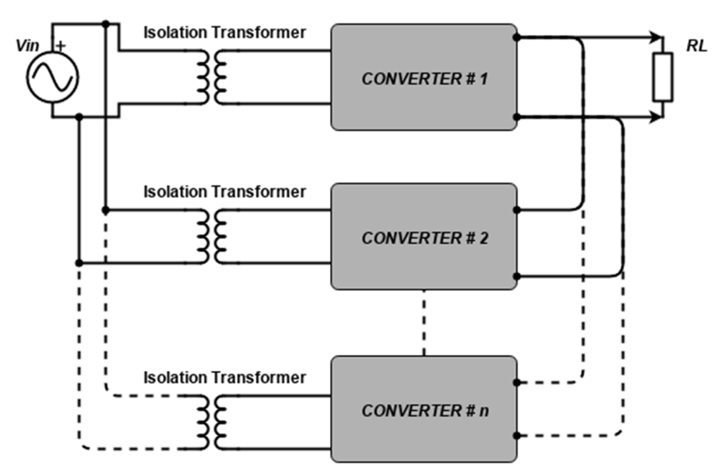
Paralleling the converter device was a concept for a more reliable system with more proper load current balancing schemes [16,17,18,19]. Based on the results in [18,19], it is concluded that paralleling the converter is more reliable than non-paralleling. However, the challenge of circulating currents is also a challenging aspect in such topologies [12,13,14], which can also lead to unbalanced load current sharing between the converters, degrading the system’s performance. Dealing with circulating currents in parallel devices can also be done via the same isolation method. The isolation can either be in the form of installing an isolation transformer at the input side after the AC supply source [5,20], shown in Figure 1, or by applying separated AC sources to each parallel-connected converter [16,21], shown in Figure 2. The approach used in previous references is not practically desirable due to the expense and bulkiness of the whole system.
The high impedance provided by the interphase reactor placing is also used to deal with circulating currents in the system [16,21]. The major challenge in this approach was the existence of low frequency circulating currents due to the little impedance from the reactor at low frequencies. Another control approach was introduced in [15,22,23,24,25,26], in which all the converters connected in parallel are taken as a single unit. This has a significant drawbacks in terms of synchronization, as a system can have converters of different brands connected in the system.
In both cases, circulating currents mainly occur due to improper current sharing between the converters, whether interleaved or paralleled. The applied control schemes primarily influence unequal current sharing in the converter’s parameters. Minimizing these mismatches is essential to address circulating currents by ensuring proper and balanced current sharing between the converters. Some methods have been proposed to control circulating currents in the literature.
For instance, in [27], circulating currents are reduced by controlling the PWM signals provided to the converters. A similar approach is presented in [7], where the average current for each phase is calculated, and control signals are individually updated based on these calculations to balance current sharing between phases. Likewise, common mode circulating currents are controlled between parallel-connected modules in [28,29] using PWM control techniques. The deadbeat control method [30] is also introduced for circulating current control, while the concept of circulating impedance [29] is introduced between converter modules to minimize circulating currents.
This article focuses on PWM-related methods to avoid the need for additional bulky and costly devices specifically designed to address circulating currents. This research aims to provide a compact PWM control scheme that effectively manages circulating currents in two commonly practiced connection topologies: interleaved and parallel. The bridgeless scheme approach introduced in this research further enhances the power system’s advantages by reducing energy losses.
This research primarily targets the Texas Instruments (TI) board (details provided later). Circuit simulations are performed explicitly on the digital replica of this TI board. The subsequent sections of the article are organized as follows: Section 2 discusses the applications of different connection topologies of power converters. Section 3 presents the bridgeless interleaved boost converter circuit, while Section 4 elaborates on the circulating current loops in the interleaved topology of the boost converter. In Section 5, two interleaved boost converter modules are connected in parallel, and circulating currents between these modules are studied. Section 6 outlines the proposed control scheme for all circulating current types within the interleaved and paralleled schemes. A stability analysis of both interleaved and parallel circuits is performed in Section 7. MATLAB/Simulink is used for software verification, and the results are presented in Section 8. The control prototype is designed for the TI prototype, and the practical results are presented in Section 9 of this article. Finally, Section 10 concludes this article.
2. Power Electronic Converter Connection Topology Applications
Power electronic converters facilitate power transfer between different energy sources, utilizing semiconductor switches for control. In modern power systems, renewable energy sources have gained widespread adoption, and power electronic converters (PECs) play a vital role in interconnecting these diverse energy sources. The efficiency of such power systems heavily relies on the efficiency of these PECs. One can focus on their different topology connections to enhance the efficiency of power converters. The design of a power converter in a system is directly related to the control of output and input currents and voltages, whereas the topology of the connections between converters significantly impacts the system’s efficiency. The main topology connections used for converters today are series, parallel, and interleaved topology, and this section discusses some of their modern-day applications.
For instance, parallel-connected uninterruptible power supplies are presented in [31], where multiple power supplies are connected in parallel to increase capacity and provide redundancy in case of a fault. This arrangement ensures a continuous power supply, even if one supply fails. Another contemporary example is presented in [32], where the load current is shared among converters to reduce stress on individual converters, thereby enhancing the system’s reliability.
Interleaved topology is another well-known arrangement employed in power converters. In electric vehicle systems, these converters are used in an interleaved scheme to increase the output power capacity of a single battery pack [33]. Similarly, the converters are used in an interleaved scheme in server power supplies to efficiently distribute power to the system’s components [34]. Apart from this, interleaved converters are also beneficial in LED lighting systems. For instance, in [35], a three-leg interleaved boost converter is utilized to achieve an efficient LED lighting power factor correction system.
The applications of these topologies mentioned above in modern work are the main motivation for this research. The novelty of this study lies in the combination of the above-discussed topologies within a single power system to leverage their collective advantages. A bridgeless scheme is employed in this work, reducing power losses within the system and positively impacting efficiency. The prototype presented in this research includes a controller design that accommodates various models of interleaved and parallel-connected converter modules. This design is particularly useful for charging electric vehicles, providing increased output voltage and current capacity. While the prototype is designed for a single-phase system, it can be adapted for future use in a three-phase connected system. To assess the effectiveness of the proposed controller, a comparison is made with some modern control schemes, such as Energy Shaped Control (ESC) and a Fuzzy Controllers, as described in a recent work [36]. This comparison evaluates the performance of the proposed controller in circulating current control, harmonics reduction, and power factor correction.
3. Bridgeless Interleaved Topology of Boost Converters
In power conversion, the AC–DC converter stage immediately follows the AC supply source to provide a DC voltage to the user. Most user appliances require a pure DC supply at the output. To achieve this, capacitive filters and rectifiers are positioned at the end of the circuit, sometimes leading to short-duration current spikes. These current spikes significantly impact the total harmonic content of the circuit, especially in high-power delivering circuits.
Two main factors are monitored for assessing the power quality of any power system: the Power Factor (PF) and Total Harmonic Distortion (THD) of the system. PF primarily concerns the efficient power consumption of the system. Power factor correctors (PFCs) are introduced to compensate for the power factor. PFCs aim to shape the input supply current with the input supply voltage, aligning them in phase and extracting the maximum input power from the AC supply source.
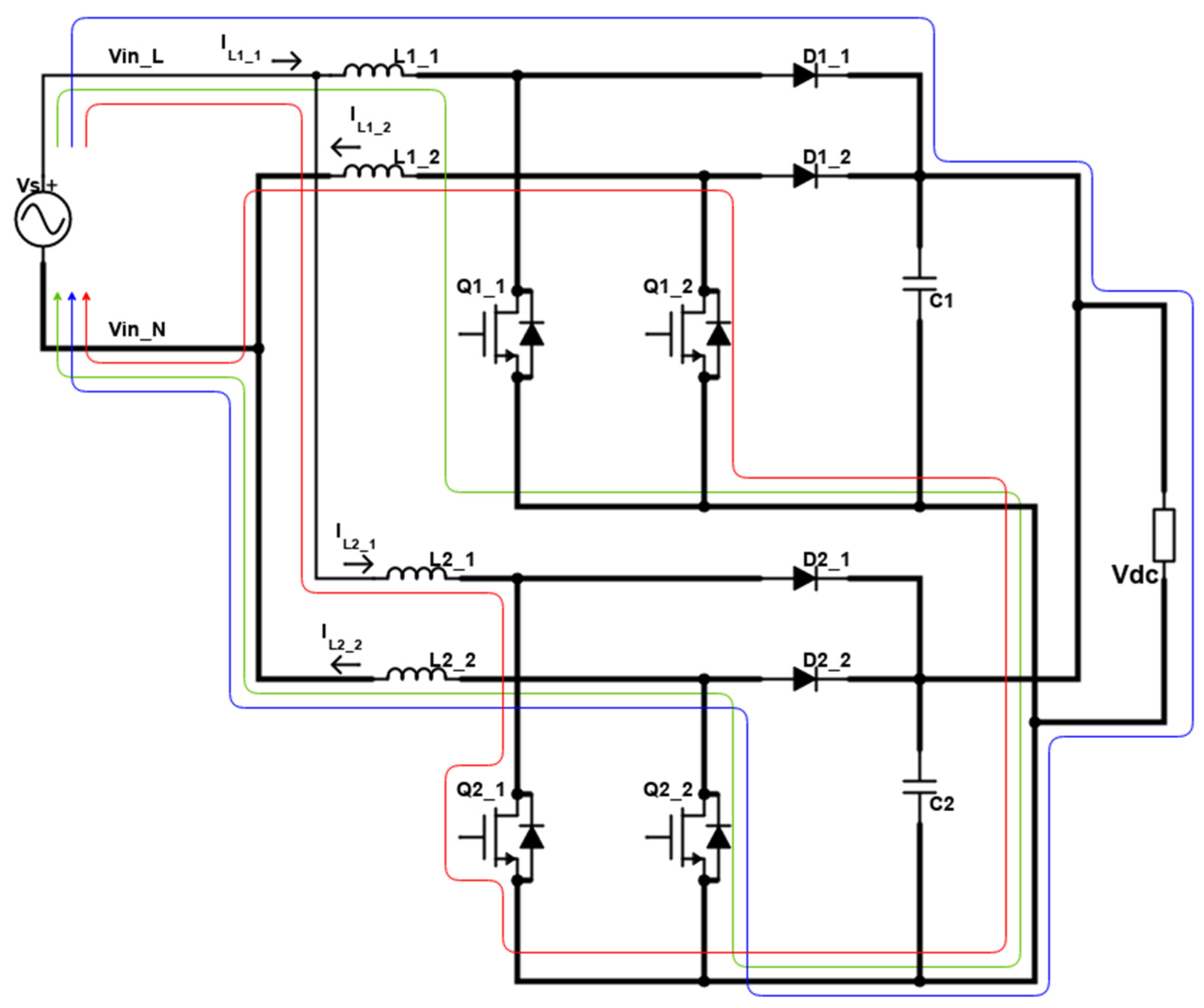
For power factor compensation, a block diagram in Figure 3 is presented, which contains the bridgeless PFC with the interleaved topology of boost converters. An input EMI filter and inrush control relay are placed between the input supply source and the PFC converter, while a capacitor filter and a load are at the outer end of the circuit. Two boost converters are connected in an interleaved scheme for each half-line cycle. The circuit’s input voltage is symmetrical in two half-line cycles, while the line current of the circuit flows only through the two diodes of the circuit, which results in low conduction losses. The space utilization and the thermal performance of the circuit improve due to the use of two inductors compared to a single conventional inductor. It can help to improve the system’s efficiency, even for higher power applications. The sum of both inductor currents, i.e., IL1_1 and IL1_2, represents the total current from the input supply source. The ripple currents will be out of phase in these inductors; therefore, they will cancel the effect of each other. This will reduce the EMI filter size by mitigating the high-frequency ripple current generated due to the high-speed switching of the boost converter. The outer capacitor’s high-frequency ripple is also reduced in this scheme.
The detailed operation of the bridgeless interleaved buck-boost converter is performed in two different cycles of the input voltage, i.e., the positive and the negative half cycle, as indicated by two different colors in Figure 3. During the positive half cycle of the input supply source, the power is transmitted from the input to the output with the help of L1_1. The switch Q1_1 is ON, and the current path is provided between the load and the input supply source via inductor L1_1. Similarly, for a negative half cycle, the power is supplied through L1_2. The circuit L1_1, Q1_1, and D1_1 act as a single boost converter, switching at a high frequency for the first positive cycle, as indicated by the blue line in Figure 3. For the negative half cycle, a link is provided between the input supply source and the output load with the help of inductor L1_2, as indicated by the red line in Figure 3. Here L1_2, Q1_2, and D1_2 behave as a single boost converter, switching at high frequency for the other cycle. The voltages Vin_L and Vin_N represent the line and the neutral voltages.
4. Circulating Current Loops in the Interleaved Topology of Boost Converters
Currents that flow in the circuit without contributing to the load current are called circulating currents. Several circulating current loops exist in the bridgeless interleaved topology scheme presented in the previous section. These loops are discussed in detail in this section of the article. The source voltage Vs is in sinusoidal form, so we consider the operation of the converter according to the two different cycles of the grid voltage, i.e., (1) Vs > 0 and (2) Vs < 0. For the power factor correction and output voltage regulations, the circuits’ working, circulating current loops, and inductor current statuses are discussed below in detail for cases (1) and (2).
4.1. Case (1): Vs > 0
As discussed in the previous section, the load is supplied by the first converter with interleaved topology for the positive half cycle. During this positive cycle, a circulating current loop originates from the source, circling back to the source without going to the load. When the switch Q1_1 is switched ON, the circulating current follows the loop path (Figure 4: green loop) back to the voltage source via the following loop.
In this case, the inductor voltage status will continue increasing as the input supply voltage positive half cycle is considered; therefore, applying KVL to this loop gives:
For the same case 1, we have a circuit condition in which both switches are off, and the current flows directly to the load (Figure 4: red loop). Therefore, the loop of the current will be:
As the supply current is now supplied to the output load, the status of the inductor voltage will decrease. Applying KVL to the loop in Figure 4 yields:
4.2. Case (2): Vs < 0
We consider the second case for the negative half cycle of the input supply source. In this case, the alternate switch Q1_2 remains ON, while the inductor voltage status remains low compared to the positive half cycle. The loop of the circulating current flowing in this case 2 (Figure 5: Green Loop) is as follows:
In this case, applying KVL will generate the same equation:
Similarly, for the same case, when we have both switches OFF, the current will go to the load via the following loop (Figure 5: red loop):
The current passes through the load, increasing the status of inductor voltage in this case. Therefore, by applying KVL, we obtain the following:
We can summarize the two cases with four different statuses in Table 1. Status A of case 1 and status D of case 2 have increasing statuses for the voltages across the inductors, while status B of case 1 and status C of case 2 have low inductor voltage statuses.
5. Two Parallel-Connected Setups of Interleaved Boost Converters
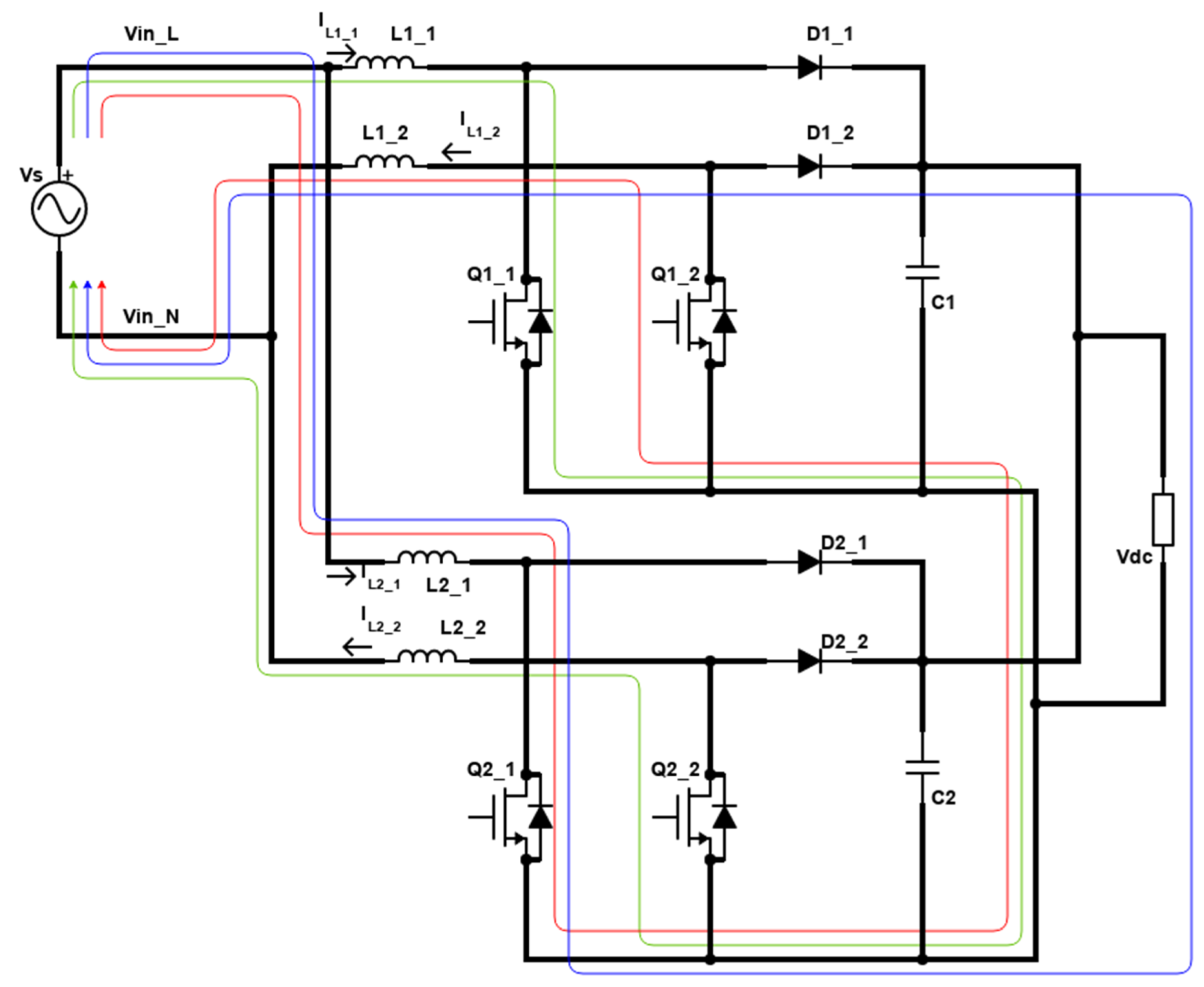
In Figure 6, two identical setups of Figure 3 are considered for parallel connections. They are connected across the same supply AC source at the input, and the load is at the output end. Here again, we are dividing the operation of the circuit into two prominent cases depending upon the status of the input supply voltage, i.e., (1) Vs > 0 and (2) Vs < 0. The converter operation in both cases, the circulating currents path, and the inductor voltage statuses are discussed below in detail.
5.1. Case (1): Vs > 0
In the parallel topology, we come across the possibility of the circulating currents moving from one setup to the other. Discussing these circulating paths, we consider different statuses according to the ON and OFF states of the switches. In case 1, the switch Q1_1 is switched ON, and the circulating current follows the path inside the circuit from one module to the other and back to the voltage source via the following loop (Figure 6: green loop):
For the same case, when the switch Q2_1 is switched ON (Figure 6: red loop), the loop of circulating current is:
The voltages for the inductors remain increasing for the above statuses (A and B) in case 1. Now, considering status C, in which all the switches are OFF, and the current flows directly towards the load (Figure 6: Blue Loop), the loop of the current will be:
5.2. Case (2): Vs < 0
In this case, the circuit is considered for the negative half cycle of the input supply source. The circulating current loop when switch Q2_2 is considered to be ON (Figure 7: green loop) is:
When switch Q1_2 is switched ON (Figure 7: red loop), the circulating current loop for the same case 2 is
The voltage status for the inductors remains decreasing in case 2. When all the switches of the converter are considered to be switched OFF, as in this case, the current will flow towards the load (Figure 7: blue loop)
All the cases and statuses of this scheme are summarized in Table 2.
6. Proposed Control Scheme
The proposed controller will be described in three steps to facilitate a better understanding of the concept behind it. First, the partial proposed controller will be introduced, which is responsible for the voltage and current control of a combined case involving interleaved and parallel-connected converters. In this step, no control mechanism for circulating currents will be included.
Next, a Common Mode Circulating Current (CMCC) controller will be integrated into the partial proposed controller. This step will focus solely on the circulating current loops associated with the interleaved case in a single-board interleaved converter.
Finally, the full form of the proposed controller will be presented, encompassing a combined case of interleaved and parallel connected converters. This comprehensive controller will consist of two separate controllers, namely the CMCC and Differential Mode Circulating Current (DMCC) controllers. The full controller will be designed to simultaneously manage the output voltage, line current, and all the circulating current control loops.
The basic design of the proposed controller is partially shown in Figure 8, which contains the cases of interleaved and parallel connected converters. The term ‘partially’ is given for Figure 8 because it generally contains the output voltage control and inner current control loops without any control for the circulating current loops described above. In total, seven feedback signals are sensed from the circuit, which latterly takes part in the controller. These signals are an output voltage Vdc, the four inductor currents (IL1_1, IL1_2, IL2_1, IL2_2), and the line (Vin_L) and neutral voltage (Vin_N) signals. We have two control loops in the controller: the outer voltage control loop and the inner current control loop. As we are dealing with two parallel devices, we have four sub-loops of the current control loops (due to the total four boost converters), which will be adjusted according to the number of parallel connected devices.
Inside the voltage control loop, the output DC voltage is sensed and compared with a reference voltage (Vdc_ref) specified by us. The difference is minimized using a voltage compensator. The output from this voltage control loop is taken as a reference value for the inner current control loops. Before providing it to the inner loop, this reference signal is multiplied by the rectified form of the input supply voltage for the addition of phase and shape. The reference signal is ready to be provided to the current control loops, where the inductor currents are subtracted from them in each loop. Again, to remove their difference, the current compensators are used. The output from these current compensators is provided to the PWM generator, which will provide the gating signals for the switches of each boost converter. At this step, this proposed controller has no control over the circulating currents.
Depending upon the topologies followed in Figure 8, there are two main types of circulating currents inside proposed modules: the Common Mode (CMCCs) and Differential Mode Circulating Currents (DMCCs). Suppose the converter module for a single setup is considered, where the converters are connected in an interleaved topology. In this case, there is a CMCC, and if two modules of such interleaved converters are connected in parallel then the circulating current will be CMCC along with DMCC.
6.1. Common Mode Circulating Current CMCC with a Controller
CMCC refers to the types of circulating currents existing inside the interleaved topology scheme. CMCC is the difference between the inductor currents of the two legs of the interleaved topology [37], i.e.,
To better understand the CMCC controller, the single board of interleaved converter (Figure 3) is considered for a control, where we only deal with two interleaved connected converters. Therefore, the control part (only) of this single board interleaved case is shown in Figure 9, which contains five feedback signals from the circuit. These signals are the output voltage signal Vdc, the two inductor currents (IL1_1, IL1_2), and the line (Vin_L) and neutral voltage (Vin_N) signals. For the full form of the proposed controller for a single interleaved module for controlling the output voltage, line current, and circulating currents, a separate CMCC controller is added to the control part of Figure 8 to minimize the common mode currents from the interleaved topology (shown by the dotted red lines in Figure 9). In Figure 9, a single current control loop is taken, whereas inside the CMCC controller, the inductor currents are subtracted from each other, while there difference is minimized by using a PI current controller. The output from this CMCC controller is then subtracted from the reference current in the current control loop. The rest of the control will remain the same for the voltage control loop. This CMCC aims to ensure equal current sharing between the two legs of the interleaved converters. Figure 9 is now the full form of the proposed controller used for a single case of an interleaved connected board. A Differential Controller is added for parallel connected boards, which is discussed below.
6.2. Differential Mode Circulating Current DMCC Controller
The DMCCs are mainly part of the parallel-connected topologies. DMCC is the difference between the inductor currents of the first leg of each parallel-connected module, i.e.,
Here, δx represents the distribution factor, and its value should be between 0 and 1: (0 < > 1). This distribution factor is given by the following:
where Px represents the power of the individual converter and Ptotal represents the system’s total power.
In this section of the controller, the full and final version of the proposed controller is presented (Figure 10) for utilization in both parallel and interleaved connected converters (Figure 6). This versatile controller is not only applicable for circulating current controls in both topologies, but also proves valuable in the control of the output voltage and inner line current. The controller comprises five distinct loops: an outer voltage control loop, two inner current control loops, and two loops of the Common Mode Circulating Current (CMCC) controller, along with the addition of the distribution factor δx. The value of this distribution factor can be adjusted to enable control of the Differential Mode Circulating Current (DMCC) for parallel-connected modules of both the same and different ratings.
7. Interleaved and Parallel Circuit Stability Analysis
7.1. Interleaved Connected Boost Converters
In a control system, a stability analysis is performed to define the stability of a system with the help of a mathematical model. For performing the stability analysis of the proposed model of the interleaved connected system (Figure 3), Kirchhoff’s law of voltage is applied to obtain the equations for the charging and discharging of the inductors:
In the above equations, L and R denote the circuit’s inductance and Series Equivalent Resistance (SER). Applying the above equation with the average state-space technique and introducing the duty cycle ratio function D will result in an equation for input supply voltage as follows:
The term d in the above equation represents a differential operator. Therefore, the above equation is the input supply voltage equation for the inductor’s charging and discharging phases. Now we can extend this equation to the parallel-connected converter circuits.
7.2. Parallel Connected Boost Converters
For the parallel-connected scheme (Figure 6), the generic representation for each interleaved converter circuit’s first and second leg is done by x and y, extending the above input supply voltage equation for both parallel-connected circuits, i.e., for the converter circuits 1 and 2 in Figure 11. This is given by the below equations.
Circulating currents can be the reason for the circuit’s performance degradation and stability problems. They can cause power losses inside the circuit, create voltage imbalances between the converters, and induce EMI into the circuit, resulting in noise induction in the connected circuit. Moreover, circulating currents can generate stability problems by interacting with attached devices, control loops, and feedback loops. Considering Figure 11, the circulating currents of any converter are represented by subtracting the assigned total current reference from the actual current of that converter [15]:
Considering k = 1 for finding the circulating current equation from converter 1 towards the converter 2 circuit, the above equation in terms of Equations (14) and (15) can be written as follows:
The above equation interprets two conditions of the circuit operation, i.e., if both converters have equal rating operations, only the output DC voltage Vdc contributes to the circulating current C1. Nevertheless, if the operating rating conditions differ for both parallel-connected converters, the AC supply input voltage Vac is added to Vdc for the circulating current C1. For a circulating current circuit, the stability problem is checked with the help of pole = −(Ra + Rb)/(La + Lb). This means that if the SER (Ra + Rb) summation is decreased, the stability margin also decreases. The system will have the lowest stability margin if the SER’s value reaches zero (which normally does not occur because the transmission lines always have some SER available). This means that the system’s stability is confirmed, as is always the case inside the left half plane. Instability occurs only when both converters operate at different power ratings. The above equation shows that the stability analysis directly correlates with SER and is inversely related to the inductance.
8. Simulation Results
Our proposed scheme has been thoroughly verified using MATLAB/Simulink. In Simulink, the proposed control scheme is demonstrated for two modules of the bridgeless boost interleaved converters connected in parallel, with the flexibility to extend it to accommodate multiple parallel modules (n numbers). For comparison, the default control method (input voltage feed-forward control scheme) of the Texas Instruments (TI) board is applied to this power system. The resulting CMCC and DMCC profiles of the system, along with their respective inductor currents, are depicted in Figure 12 and Figure 13, respectively.
The obtained results indicate that the feed-forward control scheme on the TI board exhibits a noticeable presence of CMCCs (Figure 12) and DMCCs inside the system (Figure 13). Moreover, the profile for input supply voltage and currents (Figure 14) shows that they are in phase, but the current waveform is not sinusoidal. Consequently, this scheme leads to a higher Total Harmonic Distortion (THD) system profile.
Our proposed controller has been partially applied to the system, meaning that the CMCC and DMCC controllers have not yet been implemented. The CMCC profile (without the CMCC controller) is depicted in Figure 15, while the DMCC profile (without the DMCC controller) is shown in Figure 16, along with their corresponding inductor currents. Both figures illustrate the CMCC and DMCC profiles obtained by subtracting the respective inductor currents. For the CMCC, the inductor currents of the first module’s converters are considered to demonstrate the CMCC profile. For the DMCC, the first inductor currents of the first and second modules are considered to display the DMCC profile.
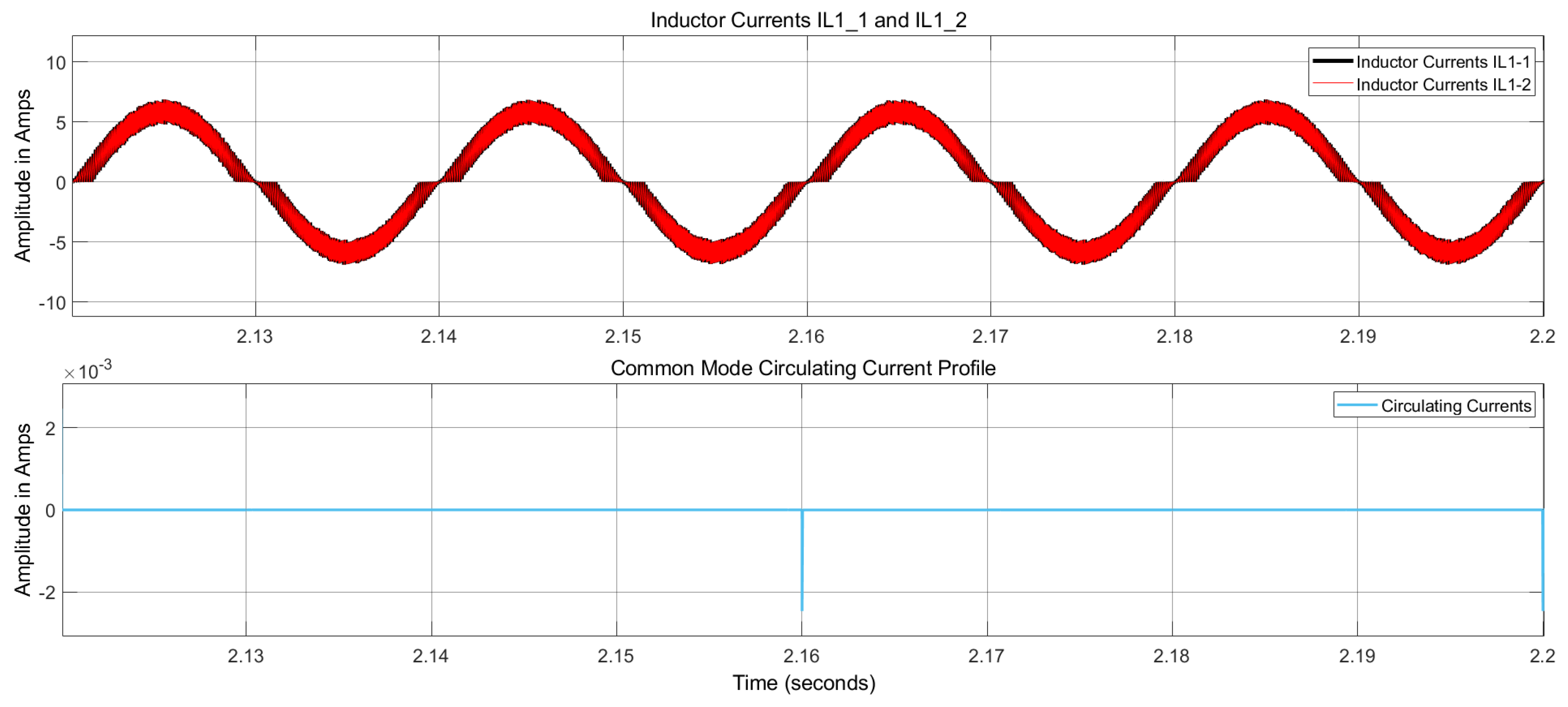
Next, the full proposed controller system, incorporating both CMCC and DMCC controllers, is introduced. Figure 17 presents the circulating current profile in a single interleaved topology module, i.e., the CMCC profile, while Figure 18 represents the circulating current profile of the two parallel-connected modules, i.e., the DMCC profile, alongside their respective inductor currents. The results demonstrate that our proposed control scheme exerts proper control over CMCCs and DMCCs, effectively reducing them from the system. Figure 19 illustrates the input supply voltage and current profiles, which are purely sinusoidal and perfectly in phase.
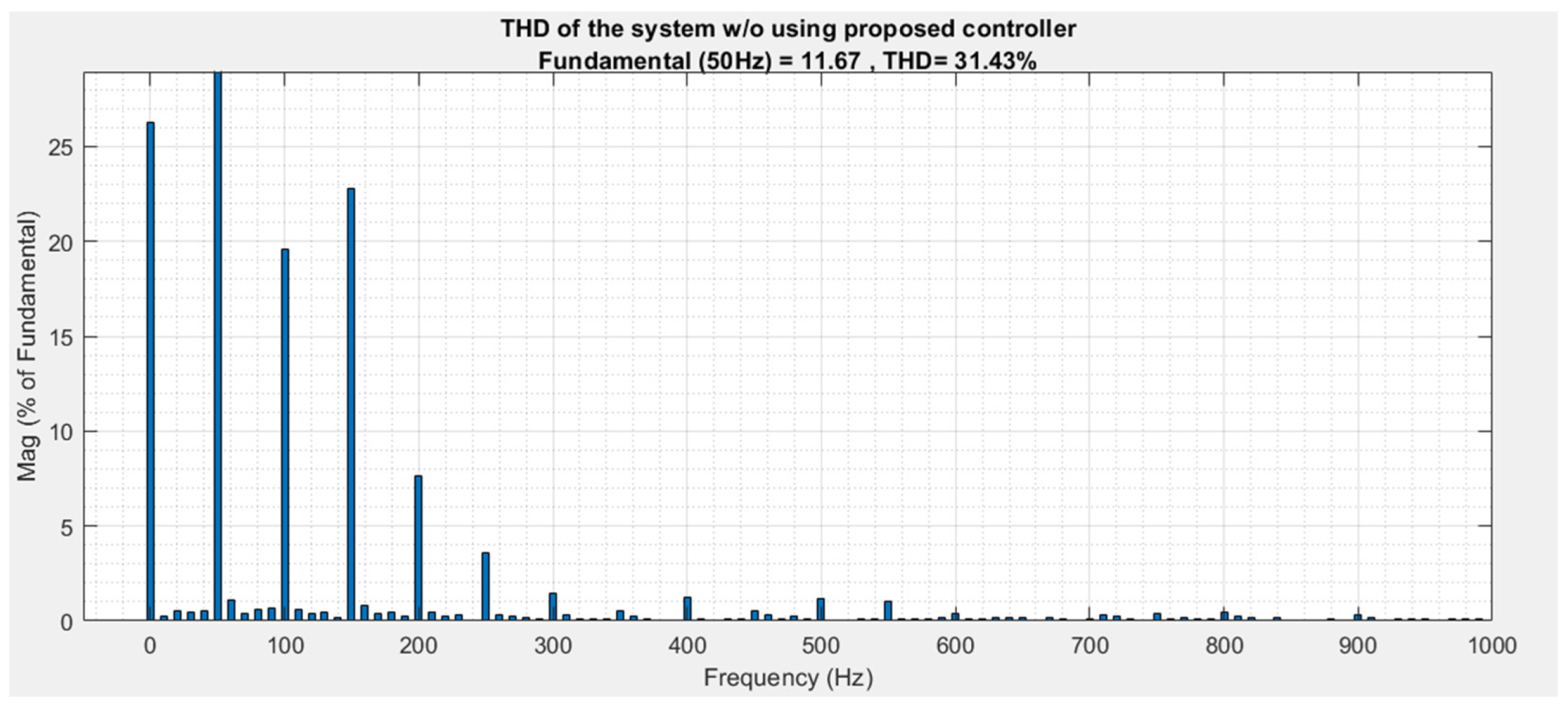
To further evaluate the effectiveness of the proposed control scheme, a THD analysis is conducted for this case study. Figure 20 displays the THD profile with the proposed controller, showcasing a lower THD and better harmonics elimination compared to Figure 21, where the THD profile is without the proposed controller.
The THD calculations in Figure 20 and Figure 21 are performed for grid current harmonics. For comparison, a parallel interleaved scheme is considered in [36], where the modern-day control systems, i.e., ESC and Fuzzy Controllers, are considered for circulating current control. ESC is a type of non-linear control system that is used for the management of energy. The system’s stability is maintained by shaping the system’s energy with the help of this ESC control system. This control scheme is primarily used in power electronics, and a motor drives the system to achieve better performance goals. On the other hand, the Fuzzy controller work is based on logic. The working scenario of this Fuzzy Controller is to provide control for the power electronics system by processing the feedback signals with mathematical logic.
These controllers and our proposed controller provide better results regarding reducing the circulating currents between the interleaved and parallel connected converters. A comparison is provided between the proposed controller and the controllers in [36] for the grid current harmonics reduction profiles, leading to high power factor corrections. Therefore, the ESC grid’s current THD profile is 13.51%, while for the Fuzzy controller, it is 7.62% [36]. Comparing these THD values with the THD of 6.20% in Figure 20 shows that the proposed control scheme provides better results regarding harmonic reductions and power factor corrections for the converters’ parallel and interleaved topology connections.
9. Experimental Results
A prototype shown in Figure 22 was constructed to validate our proposed control scheme. Two separate TI boards with Piccolo C2000 (TMS320F28035 microcontroller MCU) controllers were utilized for the experiments. The generic model of this prototype of the TI board is consistent with the one considered for our simulations, as depicted in Figure 6. These boards are equipped with boost converters for Power Factor Correction (PFC) purposes, with each panel containing two boost converters connected in the interleaved scheme. The block diagram of the complete power system along with control board are depicted in Figure 23.
Two PFC boards from Texas Instruments (TMDSHVBLPFCKIT) were connected to a common control board via an interface with the PCBs which fit in the connector in which the original microcontroller used to be mounted. These interface PCBs fed the analog signals (inductor currents, line voltages, and DC bus voltage) to the control board via coaxial cables. This control board routed the signals to the ADC pins of the LAUNCHXL-F28379D microcontroller. After executing the control algorithm, the PWM signals were generated and sent to the PFCs. The schematic diagram and PCB layout of the control board and interface boards are shown in Figure 24 and Figure 25, respectively.
The PFC boards do not feature line current sensing; therefore, a custom-made line current sensing board was used. This board contained LEM LTS 6-NP Hall-effect current sensors and a voltage divider to scale the signal to the voltage range of the ADCs. The control algorithm was implemented using the Embedded Coder Support Package in Simulink, which allows for more convenient and faster prototyping compared to low-level programming in C/C++.
The experimental setup was conducted in multiple stages. Initially, the CMCC and DMCC were monitored using the default TI control of these boards, which is based on the input voltage feed-forward control. Subsequently, our proposed controller was introduced into the experiments without applying the CMCC and DMCC controllers. Finally, the complete proposed controller was implemented, encompassing CMCC and DMCC controllers. The experimental results from Figure 26, Figure 27, Figure 28, Figure 29, Figure 30, Figure 31, Figure 32 and Figure 33 were compared to demonstrate the differences and validate the effectiveness of our proposed control scheme.
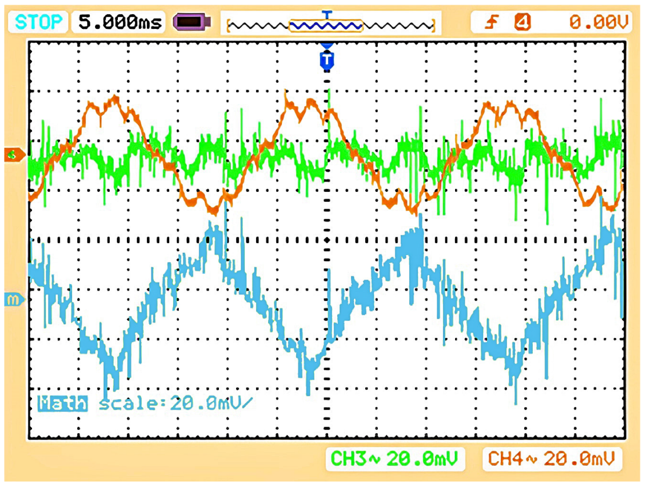
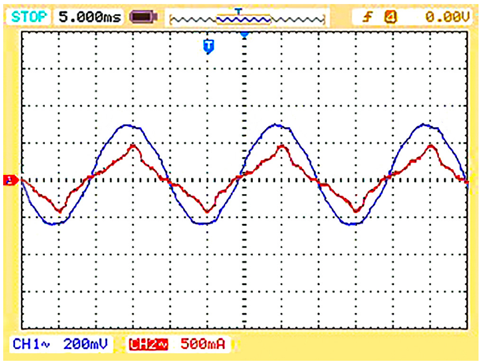
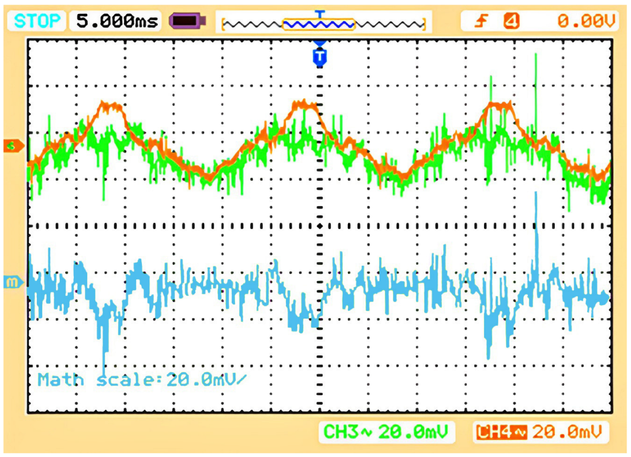
For TI default control, the experimental results are shown in Figure 26, Figure 27 and Figure 28. Figure 26 shows the CMCC profile. It can be seen that both the line currents (the first and second leg of first TI board) are in phase and have the same amplitude. Still, distortion occurred in their shape, affecting the system’s power factor (Figure 28). The DMCC profile (first line current of both parallel-connected TI boards) for the TI boards is shown in Figure 27. The difference in the shape of each line current resulted in influential circulating currents from one board to another.
Now our proposed controller is applied partially to control these boards so that only the voltage and current control loops are used without introducing the CMCC and DMCC loops. The result for this scheme follows the same pattern: Figure 29 shows the CMCC profile, while Figure 30 shows the DMCC profile of the system. It is again demonstrated that the current waveforms did not have the same amplitude, providing the paths for the circulating currents inside the same board and between the parallel-connected boards. These circulating currents are dangerous for the MOSFET switches and can damage the entire board. To reduce these currents, the CMCC and DMCC control loops were introduced to the controller to obtain the complete form of our proposed controller.
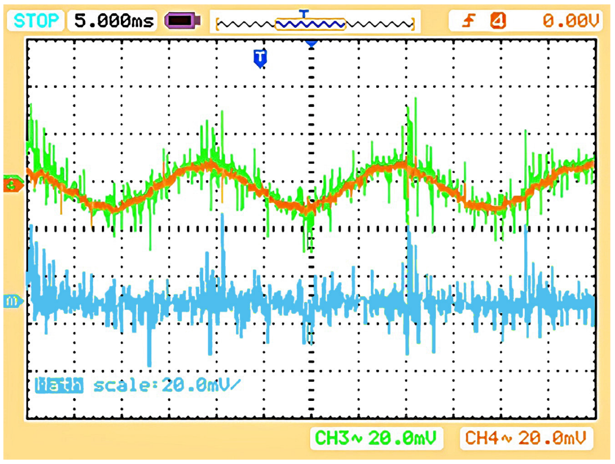
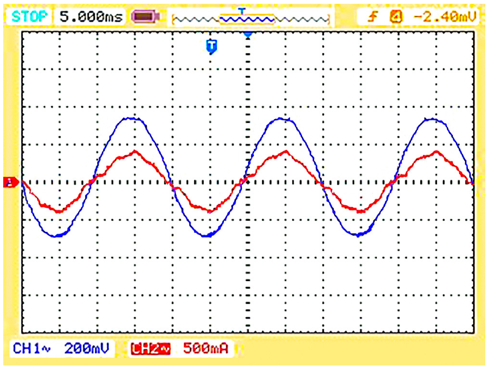
The CMCC profile for the fully applied proposed controller is given in Figure 31, which shows that both legs of the single TI boards were equal in phase and amplitude and reduced the circulating currents inside a single board. The DMCC profile given in Figure 32 shows that having nearly the same currents in the first leg of each TI board results in reduced circulating currents between the parallel-connected boards. This proposed controller will nearly provide a unity power factor of the system, as both the input supply voltage and the currents are in phase (Figure 33).
10. Conclusions
This article introduces the bridgeless interleaved topology module to demonstrate CMCC control, and these modules were connected in parallel to study and control the DMCC. This article provides a comprehensive analysis of all the possible circulating current loops for both interleaved and parallel topologies. To effectively manage these circulating currents, CMCC and DMCC controllers were introduced. For software verification, MATLAB simulations were conducted to evaluate the proposed control scheme. Additionally, a TI prototype and control boards were designed and utilized for experimental validation. The proposed control scheme was compared with the input voltage feed-forward control method, ESC, and Fuzzy Controllers regarding the harmonic elimination factor. The results demonstrate the superiority of our proposed method in effectively controlling CMCCs and DMCCs. The simulation and experimental results were thoroughly discussed to demonstrate the significant difference our proposed control method made.
Author Contributions
Conceptualization, K.J.; Methodology, K.J. and F.D.B.; Software, K.J.; Validation, K.J. and R.D.C.; Formal Analysis, F.D.B.; Resources, F.D.B.; Writing—Original Draft Preparation, K.J.; Writing—Review and Editing, K.J., R.D.C., L.V. and F.D.B.; Visualization, K.J. and R.D.C.; Supervision, L.V. and F.D.B.; Funding Acquisition, F.D.B. All authors have read and agreed to the published version of the manuscript.
Funding
This research was funded by the Higher Education Commission HEC of Pakistan, grant name “PM/HRDI-UESTPs/UETs-I/Phase-1/Batch-V/2018”. This is the primary funding for the first author’s PhD and this article.
Data Availability Statement
Not applicable.
Conflicts of Interest
The authors declare no conflict of interest.
References
- Generating Plants Connected to the Medium-Voltage Network—BDEW. Available online: https://slidelegend.com/generating-plants-connected-to-the-medium-voltage-network-bdew_59dc85e31723dd99ffe04d2a.html (accessed on 20 September 2021).
- Blaabjerg, F.; Liserre, M.; Ma, K. Power Electronics Converters for Wind Turbine Systems. IEEE Trans. Ind. Appl. 2012, 48, 708–719. [Google Scholar] [CrossRef]
- Andresen, B.; Birk, J. A high power density converter system for the Gamesa G10x 4,5 MW wind turbine. In Proceedings of the 2007 European Conference on Power Electronics and Applications, Aalborg, Denmark, 2–5 September 2007; pp. 1–8. [Google Scholar] [CrossRef]
- Gohil, G.; Bede, L.; Teodorescu, R.; Kerekes, T.; Blaabjerg, F. Line Filter Design of Parallel Interleaved VSCs for High-Power Wind Energy Conversion Systems. IEEE Trans. Power Electron. 2015, 30, 6775–6790. [Google Scholar] [CrossRef]
- Aravena, P.; Moran, L.; Burgos, R.; Dixon, J. Analysis and design of multi-stage passive filters for 100 MVA industrial power converters. In Proceedings of the 2013 IEEE Industry Applications Society Annual Meeting, Lake Buena Vista, FL, USA, 6–11 October 2013; pp. 1–7. [Google Scholar] [CrossRef]
- Asiminoaei, L.; Aeloiza, E.; Enjeti, P.N.; Blaabjerg, F. Shunt Active-Power-Filter Topology Based on Parallel Interleaved Inverters. IEEE Trans. Ind. Electron. 2008, 55, 1175–1189. [Google Scholar] [CrossRef]
- Capella, G.J.; Pou, J.; Ceballos, S.; Zaragoza, J.; Agelidis, V.G. Current-Balancing Technique for Interleaved Voltage Source Inverters With Magnetically Coupled Legs Connected in Parallel. IEEE Trans. Ind. Electron. 2015, 62, 1335–1344. [Google Scholar] [CrossRef]
- Shin, D.; Lee, J.-P.; Lee, K.-J.; Kim, T.-J.; Yoo, D.-W.; Peng, F.Z.; Ge, B.; Cha, H. 1.5MVA grid-connected interleaved inverters using coupled inductors for wind power generation system. In Proceedings of the 2013 IEEE Energy Conversion Congress and Exposition, Denver, CO, USA, 15–19 September 2013; pp. 4689–4696. [Google Scholar] [CrossRef]
- Gohil, G.; Bede, L.; Maheshwari, R.; Teodorescu, R.; Kerekes, T.; Blaabjerg, F. Parallel interleaved VSCs: Influence of the PWM scheme on the design of the coupled inductor. In Proceedings of the IECON 2014—40th Annual Conference of the IEEE Industrial Electronics Society, Dallas, TX, USA, 29 October–1 November 2014; pp. 1693–1699. [Google Scholar] [CrossRef]
- Shin, D.; Lee, K.-J.; Kim, H.-J.; Lee, J.-P.; Kim, T.-J.; Yoo, D.-W. Coupled inductors for parallel operation of interleaved three-phase voltage source grid-connected inverters. In Proceedings of the 2013 Twenty-Eighth Annual IEEE Applied Power Electronics Conference and Exposition (APEC), Long Beach, CA, USA, 17–21 March 2013; pp. 2235–2239. [Google Scholar] [CrossRef]
- Shin, D.; Lee, J.-P.; Yoo, D.-W.; Kim, H.-J. Stability Improvement of Interleaved Voltage Source Inverters Employing Coupled Inductors for Grid-Connected Applications. IEEE Trans. Ind. Electron. 2015, 62, 6014–6023. [Google Scholar] [CrossRef]
- Pan, C.-T.; Liao, Y.-H. Modeling and Coordinate Control of Circulating Currents in Parallel Three-Phase Boost Rectifiers. IEEE Trans. Ind. Electron. 2007, 54, 825–838. [Google Scholar] [CrossRef]
- Ye, Z.; Boroyevich, D.; Choi, J.-Y.; Lee, F. Control of circulating current in two parallel three-phase boost rectifiers. IEEE Trans. Power Electron. 2002, 17, 609–615. [Google Scholar] [CrossRef]
- Jacobina, C.B.; dos Santos, E.C.; Rocha, N.; Gouveia, B.d.S.; da Silva, E.R.C. Reversible AC Drive Systems Based on Parallel AC–AC DC-Link Converters. IEEE Trans. Ind. Appl. 2010, 46, 1456–1467. [Google Scholar] [CrossRef]
- Pan, C.-T.; Liao, Y.-H. Modeling and Control of Circulating Currents for Parallel Three-Phase Boost Rectifiers With Different Load Sharing. IEEE Trans. Ind. Electron. 2008, 55, 2776–2785. [Google Scholar] [CrossRef]
- Kawabata, Y.; Maekawa, T.; Kawabata, T. Novel PLL systems which suffer little influence from voltage un-balance and distortion. In Proceedings of the The 2010 International Power Electronics Conference-ECCE ASIA-, Sapporo, Japan, 21–24 June 2010; pp. 354–359. [Google Scholar]
- Holtz, J.; Lotzkat, W.; Werner, K.-H. A high-power multitransistor-inverter uninterruptable power supply system. IEEE Trans. Power Electron. 1988, 3, 278–285. [Google Scholar] [CrossRef]
- Javed, K.; Vandevelde, L.; De Belie, F. Efficiency and Transfer function calculation of the Buck-Boost con-verter with ideal flow control. In Proceedings of the 2021 23rd European Conference on Power Electronics and Applications (EPE’21 ECCE Europe), Ghent, Belgium, 6–10 September 2021; pp. 1–10. [Google Scholar]
- Matakas, L.; Giaretta, A.R. Voltage and current tracking control for the parallel connection of VSC H-bridge converters without transformer. In Proceedings of the XI Brazilian Power Electronics Conference, Natal, Brazil, 11–15 September 2011; pp. 1087–1094. [Google Scholar] [CrossRef]
- Abbes, M.; Mehouachi, I.; Chebbi, S. Circulating current reduction of a grid-connected parallel interleaved converter using energy shaping control. Electr. Power Syst. Res. 2019, 170, 184–193. [Google Scholar] [CrossRef]
- Kim, K.H.; Kim, W.D.; Hyun, D.S. A harmonic circulation current reduction method for parallel operation of ups with a three-phase PWM inverter. J. Power Electron. 2005, 5, 160–165. [Google Scholar]
- Ayano, H.; Inaba, H.; Ogasawara, S. A parallel matrix converter system. In Proceedings of the 2006 37th IEEE Power Electron-ics Specialists Conference, Jeju, Korea, 18–22 June 2006; pp. 1–7. [Google Scholar]
- Matakas, L.; Kaiser, W. Low harmonics, decoupled histeresis type current control of a multiconverter consisting of a parallel transformerless connection of VSC converters. In Proceedings of the IAS ‘97. Conference Record of the 1997 IEEE Industry Applications Conference Thirty-Second IAS Annual Meeting, New Orleans, LA, USA, 5–9 October 1997; Volume 2, pp. 1633–1640. [Google Scholar] [CrossRef]
- Terrazas, T.M.; Marafao, F.P.; Monteiro, T.C.; Giaretta, A.R.; Matakas, L.; Komatsu, W. Reference generator for voltage controlled power conditioners. In Proceedings of the XI Brazilian Power Electronics Conference, Natal, Brazil, 11–15 September 2011; pp. 513–519. [Google Scholar] [CrossRef]
- Abe, R.; Nagai, Y.; Tsuyuki, K.; Nishikawa, H.; Shimamura, T.; Kawaguchi, A.; Shimada, K. Development of multiple space vector control for direct connected parallel current source power converters. In Proceedings of the Proceedings of Power Conversion Conference—PCC ‘97, Nagaoka, Japan, 6 August 1997; Volume 1, pp. 283–288. [Google Scholar] [CrossRef]
- Fukuda, S.; Yoshida, T.; Ueda, S. Control strategies of a hybrid multilevel converter for expanding adjusta-ble output voltage range. IEEE Trans. Ind. Appl. 2009, 45, 827–835. [Google Scholar] [CrossRef]
- Ji, S.; Yong, Y.; Chunqing, Q. Control of circulating current for direct parallel grid-connected inverters in photovoltaic power generation. In Proceedings of the 2009 International Conference on Mechatronics and Automation, Changchun, China, 9–12 August 2009; pp. 3805–3810. [Google Scholar] [CrossRef]
- Tang, F.; Jin, X.; Tong, Y.; Liu, J.; Zhou, F.; Ma, L. Parallel interleaved grid-connected converters in MW-level wind power generation. In Proceedings of the 2009 IEEE International Electric Machines and Drives Conference, Miami, FL, USA, 3–6 May 2009; pp. 789–796. [Google Scholar] [CrossRef]
- Yu, M.; Kang, Y.; Zhang, Y.; Yin, M.; Duan, S.; Shan, H.; Chen, G. A Novel Decoupled Current-Sharing Scheme Based on Circulating-Impedance in Parallel multi-Inverter System. In Proceedings of the IECON 2007—33rd Annual Conference of the IEEE Industrial Electronics Society, Taipei, Taiwan, 5–8 November 2007; pp. 1668–1672. [Google Scholar] [CrossRef]
- Xiao, H.; Luo, A.; Bai, L.; Tu, C.; Zhou, J.; Liu, Q. A deadbeat control method for circulating current between parallel-connected inverters. In Proceedings of the 2013 1st International Future Energy Electronics Conference (IFEEC), Tainan, Taiwan, 3–6 November 2013; pp. 806–811. [Google Scholar] [CrossRef]
- Spears, E. Parallel UPS Configurations. Eaton–2009-Access Mode. Available online: http://www.eaton.com/Electrical/USA/WhitePapers/idcplg (accessed on 24 August 2023).
- Deng, Q.; Sun, P.; Hu, W.; Czarkowski, D.; Kazimierczuk, M.K.; Zhou, H. Modular Parallel Multi-Inverter System for High-Power Inductive Power Transfer. IEEE Trans. Power Electron. 2019, 34, 9422–9434. [Google Scholar] [CrossRef]
- Elsied, M.; Salem, A.; Oukaour, A.; Gualous, H.; Chaoui, H.; Youssef, F.T.; Belie, D.; Melkebeek, J.; Mohammed, O. Efficient Power-Electronic Converters for Electric Vehicle Applications. In Proceedings of the 2015 IEEE Vehicle Power and Propulsion Conference (VPPC), Montreal, QC, Canada, 19–22 October 2015; pp. 1–6. [Google Scholar] [CrossRef]
- Rasoulinezhad, R.; Abosnina, A.A.; Khodabakhsh, J.; Moschopoulos, G. An AC-DC Interleaved ZCS-PWM Boost Converter With Reduced Auxiliary Switch RMS Current Stress. IEEE Access 2021, 9, 41320–41333. [Google Scholar] [CrossRef]
- Musumeci, S.; Bojoi, R.; Armando, E.; Borlo, S.; Mandrile, F. Three-legs interleaved boost power factor correc-tor for high-power LED lighting application. Energies 2020, 13, 1728. [Google Scholar] [CrossRef]
- Gaddameedhi, S.; Srinivas, P. A novel fuzzy based controller to reduce circulating currents in parallel in-terleaved converter connected to the grid. Int. J. Electr. Comput. Eng. (IJECE) 2021, 11, 1130–1142. [Google Scholar] [CrossRef]
- Javed, K.; Vandevelde, L.; De Belie, F. Pulse Width Modulation Harmonic Elimination Method for Common and Differential Mode Circulating Currents. In Proceedings of the 2022 IEEE International Conference on Environment and Electrical Engineering and 2022 IEEE Industrial and Commercial Power Systems Europe (EEEIC/I&CPS Europe), Prague, Czech Republic, 28 June–1 July 2022; pp. 1–6. [Google Scholar] [CrossRef]
Figure 1.
Insulation using separate isolation transformers for each converter.

Figure 2.
Isolation using separate input supply sources for each converter.

Figure 3.
Power Flow in the interleaved boost converter circuit (a positive half-cycle is indicated by the blue color, and a negative half-cycle is indicated by the red color).
Figure 3.
Power Flow in the interleaved boost converter circuit (a positive half-cycle is indicated by the blue color, and a negative half-cycle is indicated by the red color).

Figure 4.
Case 1: Status A (loop in green) and Status B (loop in red).

Figure 5.
Case 2: Status A (loop in green) and Status B (loop in red).

Figure 6.
Parallel topology of two interleaved connected boost converter setups (Case 1: status A is the loop in green, status B is the loop in red, and status C is loop in blue).
Figure 6.
Parallel topology of two interleaved connected boost converter setups (Case 1: status A is the loop in green, status B is the loop in red, and status C is loop in blue).

Figure 7.
Case 2 of parallel topology (status D is the loop in green, status E is the loop in red, and status F is loop in blue).
Figure 7.
Case 2 of parallel topology (status D is the loop in green, status E is the loop in red, and status F is loop in blue).

Figure 8.
Partial scheme of the proposed controller.

Figure 9.
CMCC controller and voltage and current control loops.

Figure 10.
DMCC controller and CMCC controller.

Figure 11.
Circulating current loop for two parallel-connected circuits.

Figure 12.
CMCC profile (along with inductor currents) for the Texas Instruments (input voltage feed-forward) control scheme.
Figure 12.
CMCC profile (along with inductor currents) for the Texas Instruments (input voltage feed-forward) control scheme.

Figure 13.
DMCC profile (along with inductor currents) for the Texas Instruments (input voltage feed-forward) scheme.
Figure 13.
DMCC profile (along with inductor currents) for the Texas Instruments (input voltage feed-forward) scheme.

Figure 14.
Supply voltage and current profile for the Texas Instruments (input voltage feed-forward) scheme.
Figure 14.
Supply voltage and current profile for the Texas Instruments (input voltage feed-forward) scheme.

Figure 15.
CMCC profile (along with inductor currents) for a single module without applying the CMCC controller.
Figure 15.
CMCC profile (along with inductor currents) for a single module without applying the CMCC controller.

Figure 16.
DMCC profile (along with inductor currents) for two parallel connected modules without applying the DMCC Controller.
Figure 16.
DMCC profile (along with inductor currents) for two parallel connected modules without applying the DMCC Controller.

Figure 17.
CMCC profile (along with inductor currents) for the proposed controller.

Figure 18.
DMCC profile (along with inductor currents) for the proposed controller.

Figure 19.
Supply voltage and current profile for the proposed controller.

Figure 20.
THD profile of the case study for the proposed control scheme.

Figure 21.
THD profile of the case study without the proposed control scheme.

Figure 22.
A prototype that was made for practical experimental validation of the proposed scheme.

Figure 23.
Block diagram of the complete power system with control and interface boards.

Figure 24.
Schematic diagram of the control board.

Figure 25.
PCB layout of the interface boards.

Figure 26.
CMCC profile of the system with TI controllers (IL1_1 in brown, IL1_2 in dark green, and their subtraction math function in blue).
Figure 26.
CMCC profile of the system with TI controllers (IL1_1 in brown, IL1_2 in dark green, and their subtraction math function in blue).

Figure 27.
DMCC profile of the system with TI controllers (IL1_1 in brown, IL2_1 in dark green, and their subtraction math function in blue).
Figure 27.
DMCC profile of the system with TI controllers (IL1_1 in brown, IL2_1 in dark green, and their subtraction math function in blue).

Figure 28.
Input supply voltage (in blue) and current (in red) waveforms with TI controllers.

Figure 29.
CMCC profile with a partial proposed controller, i.e., without CMCC and DMCC control loops (IL1_1 in brown, IL1_2 in dark green, and their subtraction math function in blue).
Figure 29.
CMCC profile with a partial proposed controller, i.e., without CMCC and DMCC control loops (IL1_1 in brown, IL1_2 in dark green, and their subtraction math function in blue).

Figure 30.
DMCC profile with a partial proposed controller, i.e., without CMCC and DMCC control loops (IL1_1 in brown, IL2_1 in dark green, and their subtraction math function in blue).
Figure 30.
DMCC profile with a partial proposed controller, i.e., without CMCC and DMCC control loops (IL1_1 in brown, IL2_1 in dark green, and their subtraction math function in blue).

Figure 31.
CMCC profile of the system with the proposed controllers (IL1_1 in brown, IL1_2 in dark green, and their subtraction math function in blue).
Figure 31.
CMCC profile of the system with the proposed controllers (IL1_1 in brown, IL1_2 in dark green, and their subtraction math function in blue).

Figure 32.
DMCC profile of the system with the proposed controllers (IL1_1 in brown, IL2_1 in dark green, and their subtraction math function in blue).
Figure 32.
DMCC profile of the system with the proposed controllers (IL1_1 in brown, IL2_1 in dark green, and their subtraction math function in blue).

Figure 33.
Input supply voltage (in blue) and input supply current (in red) waveforms of the system with the proposed controllers.
Figure 33.
Input supply voltage (in blue) and input supply current (in red) waveforms of the system with the proposed controllers.


Table 1.
Case studies and Statuses for interleaved topology of boost converters.
| Case | Status | Q1_1 | Q1_2 | Inductor Voltage Status |
|---|---|---|---|---|
| 1 | A | ON | OFF | VL1-1, VL1-2 > 0 |
| B | OFF | OFF | VL1-1, VL1-2 < 0 | |
| 2 | C | OFF | ON | VL1-1, VL1-2 < 0 |
| D | OFF | OFF | VL1-1, VL1-2 > 0 |
Table 2.
Case Studies and Statuses for parallel connections of two setups of interleaved topology of boost converters.
Table 2.
Case Studies and Statuses for parallel connections of two setups of interleaved topology of boost converters.
| Case | Status | Q1_1 | Q1_2 | Q2_1 | Q2_2 | Inductor Voltage Status |
|---|---|---|---|---|---|---|
| 1 | A | ON | OFF | OFF | OFF | >0 |
| B | OFF | OFF | ON | OFF | ||
| C | OFF | OFF | OFF | OFF | <0 | |
| 2 | D | OFF | OFF | OFF | ON | <0 |
| E | OFF | ON | OFF | OFF | ||
| F | OFF | OFF | OFF | OFF | >0 |
Disclaimer/Publisher’s Note: The statements, opinions and data contained in all publications are solely those of the individual author(s) and contributor(s) and not of MDPI and/or the editor(s). MDPI and/or the editor(s) disclaim responsibility for any injury to people or property resulting from any ideas, methods, instructions or products referred to in the content. |
© 2023 by the authors. Licensee MDPI, Basel, Switzerland. This article is an open access article distributed under the terms and conditions of the Creative Commons Attribution (CC BY) license (https://creativecommons.org/licenses/by/4.0/).
Share and Cite
MDPI and ACS Style
Javed, K.; De Croo, R.; Vandevelde, L.; De Belie, F. Circulating Current Control in Interleaved and Parallel Connected Power Converters. Machines 2023, 11, 878. https://doi.org/10.3390/machines11090878
AMA Style
Javed K, De Croo R, Vandevelde L, De Belie F. Circulating Current Control in Interleaved and Parallel Connected Power Converters. Machines. 2023; 11(9):878. https://doi.org/10.3390/machines11090878
Chicago/Turabian StyleJaved, Khalid, Ruben De Croo, Lieven Vandevelde, and Frederik De Belie. 2023. "Circulating Current Control in Interleaved and Parallel Connected Power Converters" Machines 11, no. 9: 878. https://doi.org/10.3390/machines11090878
Note that from the first issue of 2016, this journal uses article numbers instead of page numbers. See further details here.