

Estimation Technique for IGBT Module Junction Temperature in a High-Power Density Inverter
by
 , ,
, ,
Ahmed H. Okilly
1,2 ,
,
Seungdeog Choi
3,
Sangshin Kwak
4,*,
Namhun Kim
5,
Jonghyuk Lee
1,
Hyoungjun Moon
1 and
Jeihoon Baek
1,* 1
Electrical & Electronics and Communication Engineering Department, Koreatech University, Cheonan-si 31253, Republic of Korea
2
Electrical Engineering Department, Faculty of Engineering, Assiut University, Assiut 71516, Egypt
3
Department of Electrical and Computer Engineering, Mississippi State University, Starkville, MS 39762, USA
4
School of Electrical and Electronics Engineering, Chung-Ang University, Seoul 06974, Republic of Korea
5
Department of Electrical & Electronics, Korea Polytechnic, Gumi 39257, Republic of Korea
*
Authors to whom correspondence should be addressed.
Machines 2023, 11(11), 990; https://doi.org/10.3390/machines11110990
Submission received: 15 September 2023
/
Revised: 19 October 2023
/
Accepted: 23 October 2023
/
Published: 26 October 2023
(This article belongs to the Special Issue Advanced Power Electronic Technologies in Electric Drive Systems)
Abstract
:During the last few decades, insulated-gate bipolar transistor (IGBT) power modules have evolved as reliable and useful electronic parts due to the increasing relevance of power inverters in power infrastructure, reliability enhancement, and long-life operation. Excessive temperature stresses caused by excessive power losses frequently cause high-power-density IGBT modules to fail. As a result, module temperature monitoring techniques are critical in designing and selecting IGBT modules for high-power-density applications to guarantee that temperature stresses in the various module components remain within the rated values. In this paper, a module’s different losses were estimated, a heating pipe system for the thermal power cycling technique was proposed, and finite element method (FEM) thermal modeling and module temperature measurement were performed using ANSYS Icepak software version 2022 R1 to determine whether the IGBT module’s temperature rise was within acceptable bounds. To test the proposed technique, a proposed design structure of the practical railway application with a 3.3 MW traction inverter is introduced using commercialized IGBT modules from Semikron company with maximum temperature of about 150 °C. the FEM analysis results showed that the maximum junction temperature is about 109 °C which is in acceptable ranges, confirming the appropriate selection of the employed IGBT module for the target application.
1. Introduction
Power inverters are essential components that must be properly chosen and constructed for reliable operation with heavy loads and various environmental conditions in high-power-density applications such as aerospace, electric vehicles, and railway traction systems. The increasing relevance of power inverters in power infrastructure, reliability improvement, and extended lifespan operation has led to the emergence of IGBT power modules as dependable and useful electronic components [1,2,3]. IGBT power modules’ high generated power losses convert to heat and raise temperature strains, particularly the junction temperature of the module. IGBT module failures are a critical worry for the dependability of power inverters since these temperature stressors have a substantial impact on the operation of such electronic components [4,5,6]. IGBT module failure scenarios brought on by high-temperature strains include solder joint cracks, heel cracking, bonding wire liftoff, and wire burning [7,8].
Many studies have shown and illustrated how these failure modes affect a module’s operation, such as soldering failures accounting for 34% of converter system failures [9,10]. Additionally, a survey based on over 200 products from 80 businesses found that 31% of respondents selected semiconductor-powered devices as the most fragile parts of power converters used for various power applications [11]. Furthermore, many research-ers have emphasized numerous IGBT-module-related research areas and proposed vari-ous techniques and analysis methods for the acceleration testing of these modules to es-timate failure modes in the early stages of the implementation process, such as the analy-sis of IGBT module fault causes presented in [12,13]; the various techniques of accelera-tion testing for fault diagnostic methodologies given in [14,15,16]; the analysis of parameters affecting failure modes in [17]; and the different measuring equipment used in the exper-imental environment for module fault diagnosis, such as a scanning electron microscope (SEM), X-ray, and an IR camera, as proposed in [18,19,20].
The change in the module junction temperature is the most monitored statistic in several research approaches used to analyze the fault occurrence and estimate the module lifespan span due to the thermal stress problems that a module confronts when working in high-power applications. To monitor the junction temperature under consideration, circuit-based approaches [21,22], thermal-model-based methods such as finite ele-ment methods [23,24], and experimental-measurement-based lab equipment such as IR cameras and NTC thermistor devices [25,26,27] can be applied. In addition, the change in the on-state collector–emitter voltage measured under a high load current can be used to in-dicate the junction temperature, as demonstrated in [28]. The short-circuit current of an IGBT can be measured as a temperature-sensitive parameter to estimate the junction tem-perature, as carried out in [29]. Moreover, an intelligent gate driver system was used to monitor the junction temperature based on the turn-off delay time as the parameter in [30]. In all cited references about the module junction temperature, the most difficult prob-lems for the designer to examine the module junction temperature in the laboratory before the manufacturing process are the complicated experimental setup and analysis, expensive module pricing, and high power density loading circumstances specially for the testing of the module utilized in the high power density applications such as the traction inverter systems.
Different power losses, including conduction, switching, and thermal power losses, introduce temperature cycling during the operation of an IGBT power module [31,32], and this temperature cycling profile weakens the properties of the IGBT module and shortens its useful lifetime. As a result, in the selection process of an IGBT module for a target application, loss modeling and thermal analysis of the IGBT module can be used to predict the module’s temperature based on the power losses and heat energy calculation. In this paper, a single 550 KW IGBT power module utilized on a 3.3 MW traction in-verter was treated as a case study to estimate the module’s temperature using the pro-posed approach. The proposed approach analyzes and calculates the module’s various power losses and proposes a thermal heating pipe system for thermal acceleration testing. Finally, FEM thermal modeling and analysis of the IGBT module is performed to estimate the module’s temperature.
Based on the need to estimate and monitor an IGBT module’s temperature during the pre-selection process for the module’s reliable operation under high thermal stresses, this paper’s contribution is summarized as follows: Accurate analytical and simulation mod-eling methods for an IGBT module were performed to obtain the module’s various loss components. These models are based on the device rating conditions and datasheet pa-rameters, accurately estimating the junction temperature. Furthermore, a practical and straightforward mathematical design of a heat pipe system for thermal acceleration test-ing is proposed, which can apply to any module topology with lower computation and a simple design. Furthermore, the FEM thermal modeling with the designed heat pipe sys-tem of the IGBT module enables simple and fast junction temperature estimation and the proper installation and selection of the module’s cooling system.
The rest of the paper is organized as follows: Section 2 presents the structure and the design specifications of the IGBT module under study. Section 3 introduces the IGBT module’s loss components and the calculation techniques. Section 4 presents the pro-posed design of the heat pipe system for thermal cycling testing. Section 5 illustrates the FEM thermal modeling of the IGBT module using the ANSYS Icepak software. Section 6 details the FEM thermal analysis results and discussion. Section 7 presents the conclusions and future work.
2. Three-Phase Traction Inverter with Parallel IGBT Modules
Figure 1 shows the circuit structure of the 3.3 MW traction inverter utilized in railway applications. The target traction inverter in this work is implemented using six identical IGBT power modules (part number FZ1200R33KF2C) acquired from Infineon. The mod-ules are connected in parallel with equal power sharing of 550 kW. Each module has an enclosed cabinet and is connected to a high-input DC bus bar with a voltage rating of 1500 V. The FZ1200R33KF2C module is a three-phase two-level IGBT power module with a maximum rating temperature of 150 °C [33]. Figure 2 shows the circuit schematic of module 1 in the target traction inverter. In addition, the design specifications of the module are given in Table 1.
The following power loss calculation and thermal analysis to estimate the module junction temperature under full loading conditions is performed based on module 1, and the calculation for the other modules is the same as that for module 1. This is due to the fact that the six modules in the target traction inverter are identical, individually constructed, housed in their housing, and have individual heatsinks. The steps of the proposed approach to estimate the module junction temperature are shown in Figure 3. They begin with calculating the different power losses for the modules to estimate the necessary heat energy source, followed by the design of the heat pipe system for the thermal acceleration test, and conclude with the FEM thermal modeling and analysis for the module temperature measurement.
3. IGBT Module’s Loss Components and Calculation Techniques
3.1. IGBT Module’s Loss Components
Each of the six switches in IGBT module 1 (Q1–Q6) has a transistor chip denoted as T and a diode chip denoted as D, both of which cause losses when the inverter is operating. The total power losses of a module are typically divided into two groups: (1) the main loss, which includes conduction losses and switching losses; and (2) the other loss, which includes thermal losses due to thermal resistances between the heat sink and the case (RthHC), and the case and the ambient environment (RthCA), as well as leakage losses (Pleak). Leakage losses are typically disregarded since they have a small value compared with other loss components. The following subsections present and compare two methods for calculating an IGBT module’s different power loss components, including the device rating information.
3.2. Analytical Calculation Using the Datasheet Characteristics
3.2.1. Conduction Losses Calculation
Figure 4 depicts the three-phase IGBT module 1’s single-leg equivalent. The IGBT power module’s conduction losses are affected by operational conditions such as the load current (Io = Ia1), the voltage drop across the transistor (vce), and the forward voltage across the diode (vD) chips of the IGBT module’s switches. As a result, the conduction losses of the switch Q1 (Pcon_Q1) are composed of the transistor chip’s on-state loss (Pcon_T) and the diode chip’s forward loss (Pcon_D) and can be expressed as:
Figure 5a shows the transistor chip’s equivalent circuit in the conduction state. With a series connection of a DC voltage source (vceon) reflecting the transistor’s on-state zero-current collector–emitter voltage and the collector–emitter on-state resistance (Rc), the transistor conduction voltage (Vce(t)) can be expressed as follows:
The conduction voltage calculation across the diode chip can be performed using the same approach, and using the circuit equivalent shown in Figure 5b, which results in the following:
The datasheet V–I characteristics of the transistor and diode chips of the selected IGBT module, as illustrated in Figure 6, can be used to extract the parameters Rd and Rc in Equations (2) and (3).
The on-state resistances Rc and Rd are estimated to be in the range between the maximum and typical values of the Vceon and VF (as given in the datasheet) of the transistor and diode chips, respectively, where
Then, the instantaneous value of the transistor chip conduction losses is
The transistor conduction losses over a switching period can be expressed as
Substituting (6) into (7) gives
where Icav and Icrms are the average and RMS current values of the switch Q1 transistor chip, respectively.
Inverters for traction motor applications require dead time (td) to prevent cross-conduction, which occurs when the upper and lower arms of the IGBT generate a direct short-circuit across the power supply and GND lines [34,35]. As shown in the waveforms in Figure 7, the dead time is the time when both the upper-arm and lower-arm IGBTs are turned off, and the dead time is inserted to force off both the upper-arm and lower-arm IGBTs to ensure they are never on simultaneously while switching [36].
Assuming that the inverter is working in linear modulation mode with inverter modulation index m, frequency ω, load voltage-current angle Փ, and dead time td as shown in Figure 7, the conduction time of the transistor (tcon_T(t)) and diode (tcon_D(t)) during one switching period tsw can be computed as follows:
Assuming the output current equation is written as:
The transistor conduction losses for (tcon_T(t)) conduction time can be calculated using Equation (8) as:
where the Icav and Icrms can be expressed as:
Similarly, the instantaneous value of the diode conduction losses is
The average conduction losses from the diode chip can be expressed as
where IDav is the average diode current, and IDrms is the RMS diode current, which for the three-phase two-level inverter circuits, can be expressed as:
3.2.2. Switching Losses Calculation
The IGBT module switching losses (Psw) contain two components:
- The first is the transistor switching losses, which occur during the transition between the on-state and off-state of the transistor and contain the turn-on losses (Psw_onT) and the turn-off losses (Psw_offT).
The transistor switching loss over one switching period is
The switching losses of the transistor depend on the energy required to turn on (Eon) and turn off (Eoff) the transistor, which is a function of the transistor current, switching frequency, the junction temperature, and the input DC voltage and can be expressed as
where Vin traction is the DC input voltage used for the target traction inverter, and Vin datasheet is the DC input voltage from which the module datasheet characteristics are obtained.
Assuming the junction temperature to be constant over one period of the output waveform, Vin is also constant during the switching period. Therefore, the switching energy depends on the IC variation, as shown in the transistor characteristics illustrated in Figure 8a.
- The second component is the diode reverse recovery loss (Prr_D) which also depend on the reverse recovery energy (ErcD) of the diode and can be expressed as:
For the constant junction temperature, the reverse recovery energy depends on the IF variation, as shown in the diode characteristics illustrated in Figure 8b.
3.3. Simulation Estimation Using the Module Rating Information
Figure 9 shows the PSIM simulation model of the three-phase two-level inverter using the model of the FZ1200R33KF2C IGBT module in the thermal module database. The module datasheet parameters and characteristics are entered into the software to estimate the power losses based on the device rating information. The three-phase PWM generator with dead time control is used to generate the six PWM signals for the module switches.
The advantage of the PSIM simulation technique compared with analytical calculations is that it is a faster, simpler, and more accurate technique since there is no approximation where the exact device rating information is considered in calculations. Furthermore, the module thermal power losses can be directly calculated with the known values of the module’s thermal resistances.
The thermal losses (Pth) are the losses due to thermal resistance (Rth), which is the sum of the thermal resistances between the case and heat sink and between the heat sink and the environment. The thermal resistance provided in the datasheet is typically given in °K/Kw (degrees Kelvin per kilowatt) or °C/W (degrees Celsius per watt). For example, If the datasheet specifies Rth = 5 °K/kW, this means that for every kilowatt of power dissipated, the temperature difference between the case and the heatsink is 5 °K.
In this work, the three-phase PWM generator with dead time control was implemented as depicted in Figure 10. Figure 10a shows the load voltage comparator of the designed three-phase inverter module. The sine wave reference voltage was used with phase differences of 0, −120, and −240 for the three phases (A, B, and C), respectively. The PWM signals for the switches in the inverter’s three legs were decided based on the comparator output and using a 5 us dead time between the operation of the switches in the inverter’s three legs, as depicted in the sequence in Figure 10b. In Figure 10b, the Ad## 5u is the delay time used for the PWM signal.
3.4. IGBT Module Power Losses Calculation Results and Comparison
Figure 11 shows the PSIM simulation results of the reference voltage waveform of the inverter phase A with the carrier waveform and the generated PWM signals from the designed control loop for the switches Q1 and Q2. For the comparison evaluation between the power loss calculations using the analytical and simulation techniques, the dead time with 5 us was also considered in the PSIM simulation modeling, as shown in Figure 11.
With an input DC voltage of 1500 V and rated output inductive load of 550 kW, 60 Hz, and 0.7 pf, the waveforms of the conduction losses of the switch Q1 transistor (Pcond_Q1_T) and diode (Pcond_Q1_D) are plotted in Figure 12. The average conduction losses of both the transistor and diode were also estimated over a switching period and calculated as approximately 331.40 W for the transistor and approximately 91.97 W for the diode.
Figure 13 shows the waveforms of the switching losses of the switch Q1 transistor (Psw_Q1_T), and diode (Psw_Q1_D). The average switching losses of both the transistor and diode were estimated over a switching period and calculated as approximately 412.08 W for the transistor and approximately 84.06 W for the diode.
Furthermore, the total conduction and switching loss waveforms of the switch Q1 and the whole IGBT module 1 are plotted in Figure 14, where the switch Q1 total losses are estimated at approximately 919.51 W, and the module 1 total power losses are approximately 5577 W. The IGBT module thermal losses can be calculated as the difference between the module’s total losses (5577 W) and the sum of the conduction and switching losses for the six switches (5517 W), calculated as approximately 60 W for the module.
To conduct a comparison study between the analytical and simulation techniques for the IGBT module power loss calculation, Table 2 shows the values of the different power loss components of the IGBT module using both techniques and the mismatch percentage, which was less than 8% for all of the loss components calculations. In addition, Figure 15 shows the module’s total power losses with different loading conditions from 20% (110 kW) to 120% (660 kW), with a mismatch of less than 5% between both techniques.
4. IGBT Module Heat Pipe System Design Technique
Figure 16 shows the structure of the proposed heat pipe system designed for the thermal acceleration testing of the target IGBT module based on the module’s total power loss calculated in the previous section. Three heating pipes are used to generate the heat energy required for the three-phase IGBT module’s three legs. The three heat pipes are identical and symmetrically distributed along the cross-sectional area of the IGBT module heatsink. High-temperature liquid water is used at the inlet of each heat pipe, and the water temperature in the heat pipes drops due to heat loss [37] to heat the space in the IGBT module.
Assuming the water temperature is approximately T1 °C at the inlet point due to the energy loss to heat the IGBT module, the water temperature at the outlet point is assumed to drop to an ambient temperature of approximately T2 °C. The constant-pressure specific heat capacity of the water Cp can be obtained at the average temperature of (T1 + T2)/2 °C from the standard tables [37], and then the rate of heat energy loss in all pipes can be calculated as
where N is the heat pipes number, ∆T is the water temperature difference between the inlet and outlet, and m· is the mass flow rate per pipe.
The rate of energy losses in joules is equal to the total power loss over the time calculated using the analytical or simulation techniques for the IGBT loss model in Section 3 (for the worst case, the largest calculated value using the two techniques is used in the design of the heat pipe system).
The density of the water at the inlet point is
where P is the operating pressure, R is the specific gas constant for the water, and T is the temperature at the inlet in Kelvin.
The cross-sectional area of the heat pipe (Ap) with pipe diameter D is calculated as
Then, the average velocity of the water (γ) at any point inside the heat pipe can be calculated as a function of the mass flow rate:
Substituting (20), (21), and (22) into (23) gives
In (23), for the specified total energy losses the D is constant (we used a heat pipe with a diameter of approximately 8.5 mm), the inlet water temperature (T1) has a high value and is less than the water boiling degree, and T2 is the ambient temperature. According to the selected T1 and T2, the Cp coefficient can be obtained as shown in the operating curves depicted in Figure 17a, and the water velocity can be calculated via (25), as shown in Figure 17b.
As shown in Figure 4, the next step after the heat pipe system design is the FEM thermal modeling of the IGBT module to estimate the temperatures of the module’s different components and ensure that the temperature values remain within the rated values specified for the IGBT module’s use before the manufacturing process of the target traction inverter.
5. IGBT Module Thermal Modelling and Analysis
Power electronics designers can improve product reliability by using ANSYS thermal analysis software (version 2022 R1) and solutions, such as the ANSYS Icepak package, to predict how their designs will behave when operation conditions change. This allows them to solve the most challenging thermal issues, see temperature changes, and prevent overheating issues. For example, during the thermal analysis of an IGBT unit, we can check how hot the components are and whether or not our design is working as intended. The next subsections demonstrate how in our research, we used this ANSYS solution to create a FEM thermal model of the IGBT module and predict its temperature.
5.1. IGBT Module’s Structure and Material Study
Figure 18 shows the construction of the IGBT module under study with part number FZ1200R33KF2C. The IGBT module chips are produced from silicon, and the ceramics are coated with copper, which is firmly bonded to the ceramic to realize direct copper bonding (DCB) with the IGBT. The aluminum–silicon carbide (AlSiC) used to manufacture the module base plate enables it to have a low coefficient of thermal expansion (CTE), which is made possible by adjusting the composition of Al and SiC to create a surface that has a low enough CTE for the direct attachment of electronic components. The module comes with a heatsink made from aluminum (Al) with a density of approximately 2700 (Kg/m3). Table 3 shows the properties of the IGBT module material. The module properties are provided as an input parameters to the software during the FEM thermal analysis process.
5.2. IGBT Module Geometry Clean-Up
Figure 19 shows the different views of the IGBT module simulated in the ANSYS Ice-pak thermal simulation software (version 2022 R1). For the three-phase two-level IGBT module, the number of required heat pipes is N = 3, and heat pipes with a diameter of D = 8.5 mm and length of 250 mm are used and distributed symmetrically along the heatsink of the module as shown in Figure 19. The module FZ1200R33KF2C dimensions are W:140 mm, L:190 mm, D:38 mm. The module’s housing is considered in the thermal modeling of the IGBT mod-ule to show the effect of the module’s housing use on the component’s temperature values. All dimensions and distances between the module’s different semiconductor parts and different materials were obtained from the module datasheet [33] and used in the software to simulate the target IGBT mmodule as shown in Figure 19.
5.3. Boundary Conditions Setup
Figure 20 shows the IGBT module structure inside the cabinet with the boundary conditions for the module cabinet airflow and the designed heat pipe system water flow. The temperature of the water at the inlet point was selected at 60 °C and as given in Figure 17, the water flow at that temperature value is about 0.07 m/s, and the airflow set at 0.01 m/s which is the velocity of the airflow in the place which the target inverter will be used. The module is enclosed in an isolated cabinet (adiabatic) open on both sides to allow air to enter and exit. The three water pipes have equal water flow rates and open at the outlet point. The internal and external boundary conditions for the IGBT module are given in Table 4.
6. FEM Thermal Analysis Results and Discussion
Table 5 shows the setup for the thermal analysis of the IGBT module with the designed heat pipe system to measure the module temperature. The laminar flow model under the steady state condition was used to solve the water and air flows, and the temperature (energy) was used as the solving variable with a target convergence of approximately 0.001 for the flow and approximately 1 × 10⁻¹⁵ for the energy. Two running modes of the software can be used, the first one is that the number of iterations is imposed at the beginning, considering that the steady state will be reached within that number of iterations, this method is usually use of the software to conduct the same analysis and find out the most appropriate iterations number needed to reach the desired solution. The second one is the free run mode where the convergence criteria of the flow and energy are imposed in the begaining and the analysis is free running until the convergence criteria is achieved, and the steady state condition is reached.
The heat energy source for each semiconductor component of the IGBT module was specified for the thermal simulation process, and the residual values (the difference between the specified and calculated values) of the different variables were monitored with the iterations. Figure 21 shows the monitoring curves of the velocity, continuity, and energy residual values with 100 iterations during the thermal loading, showing that the constant residual value of less than the specified convergence rate was obtained for each variable after approximately 60 iterations.
Figure 22 shows the temperature point monitoring of the semiconductor chips (transistor (T) and diodes (D)) with iteration numbers, showing that the maximum measurement temperature for all semiconductor chips was measured at approximately 109 °C. This value is less than the target maximum junction temperature for the design, which is approximately 125 °C, and less than the selected IGBT module maximum rating temperature, which is approximately 150 °C.
Figure 23 shows the measurement contour for the water flow velocity inside the heat pipes. The contour shows that the velocity at the inlet point was approximately 0.07 m/s, as specified in the design. Moreover, the water velocity changes along the heat pipe from the inlet to the outlet point due to the change in the water temperature value. Figure 24 shows the measurement contour of the airflow velocity inside the module cabinet, showing that the velocity at the inlet was approximately 0.01, as specified; the changing velocity along the cabinet from the inlet to the outlet due to the change in the temperature; and the effect of the module housing on the airflow shape and velocity inside the cabinet.
To estimate the module’s different components’ temperatures, Figure 25 and Figure 26 show the temperature measurement contour of the IGBT module, including the housing, which shows that the maximum temperature measured in the transistor semiconductor chips was approximately 109.60 °C in the lower semiconductor switches. Moreover, the maximum temperature measured in the diode chips in the lower semiconductor switches was approximately 105.25 °C.
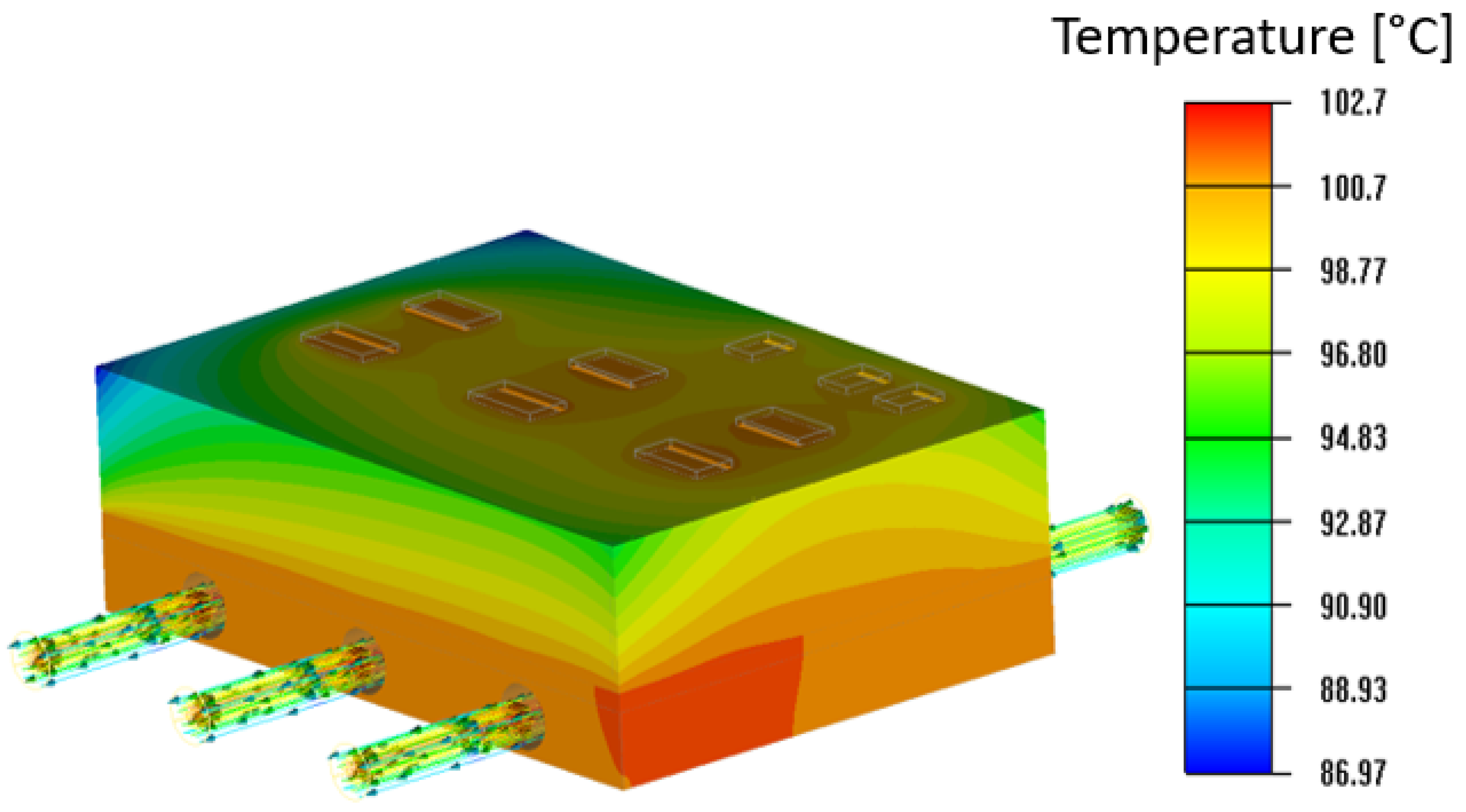
The module’s housing was removed, and the thermal analysis was performed again to estimate the temperature values without using the module housing. As shown in Figure 27, the maximum temperature measured in the transistor semiconductor chips was approximately 102.7 °C with a reduction of approximately 6.90 °C compared with using the module housing. Furthermore, the maximum temperature measured in the diode chips was approximately 99.10 °C, with a reduction of approximately 6.15 °C compared with using the module housing. Table 6 shows the numerical values of the temperature measurements in the semiconductor chips in the IGBT module with and without using the module housing.
Finally, from the analysis and the results obtained from the proposed estimation technquie, as compared with the previous temperature measurement technquies of the IGBT module, the benfits of the proposed technique to estimate the IGBT module junction temperature can be summarized in the following:
- The ability to apply for the estimation of the temperature range for any IGBT module, with any loading condition using simple calculations of the module power losses and thermal model analysis.
- Offers the ability to confirm the appropriate selection of the IGBT module for the target application before the manufacturing process.
- Saving the time and money required for the testing process to check the module junction temperature as compared with the other experimental setup techniques.
- Temperature measurements with high accuracy since no ideal components and no assumptions (datasheet parameters and the actual model performance are used in the analysis) are used in the analysis which offers the results closet to the practical reality.
7. Conclusions and Future Work
This study described the implementation of a 3.3 MW traction inverter with parallel IGBT modules for high reliability and extended lifetime, as well as the estimation of the module’s junction temperature. This paper presented two methods for calculating the power loss of IGBT modules: the first is a mathematical calculation based on device datasheet characteristics, and the second is a simulation estimation based on the loss modeling of the module including device rating information. The findings using the two methodologies were compared, and there was a mismatch of less than 8% in the calculations of the module’s distinct power loss components and of less than 5% in the calculations of the module’s total power losses. The power losses generated in the IGBT module were often converted to heat, raising the module temperature, particularly the switch junction temperature. Therefore, to ensure the high dependability of the design and module selection before the manufacturing process.
Furthermore, this paper evaluated the module junction temperature under the following operating conditions: The heat energy sources of the IGBT module were estimated based on the calculated module power losses, the design of the heat pipe system was proposed to perform the thermal loading process of the IGBT module, the FEM thermal analysis of the target IGBT module was performed in ANSYS Icepak, and the temperatures of the various components were measured. The thermal analysis revealed that the maximum junction temperature of the module under the target operation conditions was approximately 109.60 °C when enclosed in the housing and approximately 102.70 °C when not enclosed in the housing, which is less than the target design value (125 °C) and also less than the module’s maximum temperature value (150 °C), confirming the appropriate selection of the employed IGBT module for the target application with simple technique without needing of the experimental setup which saved the time and money.
In future work, to increase the dependability and useful lifetime of the IGBT module in our application, a new water-cooling system designed to lower the maximum junction temperature to less than 100 °C will be built. Additionally, replacing the air cooling system in the planned IGBT module with a water cooling system allows for high power density operation without the need to add more modules, saving money and allowing for a more compact design of the target traction inverter. Another technique which can be used to measure the module junction temperature through an experimental setup such as PWM power cycling technique will be performed by designing the power and PWM control circuits of the target inverter and measuring the junction temperature with the full loading condition. Then, the module lifetime can be estimated, and the temperature measurements using the power cycling technique and the thermal cycling technique will be compared.
Author Contributions
Design and application, A.H.O., S.C., S.K. and N.K.; Literature review, manuscript preparation and simulations, A.H.O. and J.B.; investigation, J.L. and H.M.; funding acquisition, S.K.; Final review of manuscript, corrections, A.H.O., S.C. and J.B. All authors have read and agreed to the published version of the manuscript.
Funding
This work was supported by the Korea Electric Power Corporation under Grant R21XO01-3 and fundeded by Education and Research promotion program of KOREATECH in 2023.
Data Availability Statement
Not applicable.
Conflicts of Interest
The authors declare no conflict of interest.
References
- Abuelnaga, A.; Narimani, M.; Bahman, A.S. A review on IGBT module failure modes and lifetime testing. IEEE Access 2021, 9, 9643–9663. [Google Scholar] [CrossRef]
- Xiao, D. On Modern IGBT Modules: Characterization, Reliability and Failure Mechanisms. Master’s Thesis, Institutt for elkraftteknikk, Trondheim, Norway, 2010. [Google Scholar]
- Abuelnaga, A.; Narimani, M.; Bahman, A.S. Power electronic converter reliability and prognosis review focusing on power switch module failures. J. Power Electron. 2021, 21, 865–880. [Google Scholar] [CrossRef]
- Suh, I.W.; Jung, H.S.; Lee, Y.H.; Choa, S.H. Numerical prediction of solder fatigue life in a high power IGBT module using ribbon bonding. J. Power Electron. 2016, 16, 1843–1850. [Google Scholar] [CrossRef]
- Peyghami, S.; Blaabjerg, F.; Palensky, P. Incorporating power electronic converters reliability into modern power system reliability analysis. IEEE J. Emerg. Sel. Top. Power Electron. 2020, 9, 1668–1681. [Google Scholar] [CrossRef]
- Haque, M.S.; Moniruzzaman, M.; Choi, S.; Kwak, S.; Okilly, A.H.; Baek, J. A Fast Loss Model for Cascode GaN-FETs and Real-Time Degradation-Sensitive Control of Solid-State Transformers. Sensors 2023, 23, 4395. [Google Scholar] [CrossRef] [PubMed]
- Ciappa, M. Selected failure mechanisms of modern power modules. Microelectron. Reliab. 2002, 42, 653–667. [Google Scholar] [CrossRef]
- Choi, U.M.; Blaabjerg, F.; Lee, K.B. Study and handling methods of power IGBT module failures in power electronic converter systems. IEEE Trans. Power Electron. 2014, 30, 2517–2533. [Google Scholar] [CrossRef]
- Lu, Y.; Christou, A. Prognostics of IGBT modules based on the approach of particle filtering. Microelectron. Reliab. 2019, 92, 96–105. [Google Scholar] [CrossRef]
- Kumar, D.; Nema, R.K.; Gupta, S. Development of a novel fault-tolerant reduced device count T-type multilevel inverter topology. Int. J. Electr. Power Energy Syst. 2021, 132, 107185. [Google Scholar] [CrossRef]
- Yang, S.; Bryant, A.; Mawby, P.; Xiang, D.; Ran, L.; Tavner, P. An industry-based survey of reliability in power electronic converters. IEEE Trans. Ind. Appl. 2011, 47, 1441–1451. [Google Scholar] [CrossRef]
- Li, L.; He, Y.; Wang, L.; Wang, C.; Liu, X. IGBT lifetime model considering composite failure modes. Mater. Sci. Semicond. Process. 2022, 143, 106529. [Google Scholar] [CrossRef]
- Chen, J.; Yang, Z.G. Failure analysis on the premature delamination in the power module of the inverter for new energy vehicles. Eng. Fail. Anal. 2023, 143, 106915. [Google Scholar] [CrossRef]
- Cheng, Y.; Fu, G.; Jiang, M.; Xue, P. Investigation on intermittent life testing program for IGBT. J. Power Electron. 2017, 17, 811–820. [Google Scholar] [CrossRef]
- Sarkany, Z.; Rencz, M. Methods for the Separation of Failure Modes in Power-Cycling Tests of High-Power Transistor Modules Using Accurate Voltage Monitoring. Energies 2020, 13, 2718. [Google Scholar] [CrossRef]
- Hernes, M.; D’Arco, S.; Antonopoulos, A.; Peftitsis, D. Failure analysis and lifetime assessment of IGBT power modules at low temperature stress cycles. IET Power Electron. 2021, 14, 1271–1283. [Google Scholar] [CrossRef]
- Sathik, M.H.; Sundararajan, P.; Sasongko, F.; Pou, J.; Natarajan, S. Comparative analysis of IGBT parameters variation under different accelerated aging tests. IEEE Trans. Electron. Devices 2020, 67, 1098–1105. [Google Scholar] [CrossRef]
- Hu, Z.; Du, M.; Wei, K. Real-time monitoring solder fatigue for IGBT modules using case temperatures. HKIE Trans. 2017, 24, 141–150. [Google Scholar] [CrossRef]
- Gao, T.; Ding, L.; Wang, J.; Chen, W.; Fan, X. Analysis of Blocking Capability Failure Mechanism in IGBT Module under High Salt Spray Environment. IEEE Trans. Dielectr. Electr. Insul. 2023. [Google Scholar] [CrossRef]
- Ma, Y.; Li, J.; Dong, F.; Yu, J. Power cycling failure analysis of double side cooled IGBT modules for automotive applications. Microelectron. Reliab. 2021, 124, 114282. [Google Scholar] [CrossRef]
- Eleffendi, M.A.; Yang, L.; Agyakwa, P.; Johnson, C.M. Quantification of cracked area in thermal path of high-power multi-chip modules using transient thermal impedance measurement. Microelectron. Reliab. 2016, 59, 73–83. [Google Scholar] [CrossRef]
- Li, W.; Li, G.; Sun, Z.; Wang, Q. Real-time estimation of junction temperature in IGBT inverter with a simple parameterized power loss model. Microelectron. Reliab. 2021, 127, 114409. [Google Scholar] [CrossRef]
- Shahjalal, M.; Shams, T.; Hossain, S.B.; Ahmed, M.R.; Ahsan, M.; Haider, J.; Goswami, R.; Alam, S.B.; Iqbal, A. Thermal analysis of Si-IGBT based power electronic modules in 50kW traction inverter application. e-Prime-Adv. Electr. Eng. Electron. Energy 2023, 3, 100112. [Google Scholar] [CrossRef]
- Qian, C.; Gheitaghy, A.M.; Fan, J.; Tang, H.; Sun, B.; Ye, H.; Zhang, G. Thermal management on IGBT power electronic devices and modules. IEEE Access 2018, 6, 12868–12884. [Google Scholar] [CrossRef]
- Yang, Y.; Zhang, Q.; Zhang, P. A fast IGBT junction temperature estimation approach based on ON-state voltage drop. IEEE Trans. Ind. Appl. 2020, 57, 685–693. [Google Scholar] [CrossRef]
- Ma, M.; Yan, X.; Guo, W.; Yang, S.; Cai, G.; Chen, W. Online junction temperature estimation using integrated NTC thermistor in IGBT modules for PMSM drives. Microelectron. Reliab. 2020, 114, 113836. [Google Scholar] [CrossRef]
- Bahman, A.S.; Ma, K.; Ghimire, P.; Iannuzzo, F.; Blaabjerg, F. A 3-D-lumped thermal network model for long-term load profiles analysis in high-power IGBT modules. IEEE J. Emerg. Sel. Top. Power Electron. 2016, 4, 1050–1063. [Google Scholar] [CrossRef]
- Cao, H.; Ning, P.; Chai, X.; Zheng, D.; Kang, Y.; Wen, X. Online monitoring of IGBT junction temperature based on V ce measurement. J. Power Electron. 2021, 21, 451–463. [Google Scholar] [CrossRef]
- Xu, Z.; Xu, F.; Wang, F. Junction Temperature Measurement of IGBTs Using Short-Circuit Current as a Temperature-Sensitive Electrical Parameter for Converter Prototype Evaluation. IEEE Trans. Ind. Electron. 2015, 62, 3419–3429. [Google Scholar] [CrossRef]
- Zhang, Z.; Dyer, J.; Wu, X.; Wang, F.; Costinett, D.; Tolbert, L.M.; Blalock, B.J. Online Junction Temperature Monitoring Using Intelligent Gate Drive for SiC Power Devices. IEEE Trans. Power Electron. 2019, 34, 7922–7932. [Google Scholar] [CrossRef]
- Lim, H.; Hwang, J.; Kwon, S.; Baek, H.; Uhm, J.; Lee, G. A study on real time IGBT junction temperature estimation using the NTC and calculation of power losses in the automotive inverter system. Sensors 2021, 21, 2454. [Google Scholar] [CrossRef]
- Zhu, Y.; Xiao, M.; Su, X.; Yang, G.; Lu, K.; Wu, Z. Modeling of conduction and switching losses for IGBT and FWD based on SVPWM in automobile electric drives. Appl. Sci. 2020, 10, 4539. [Google Scholar] [CrossRef]
- FZ1200R33KF2C—Module Datasheet Technical Information, Infineon. Available online: https://datasheetspdf.com/pdf-file/1439925/Infineon/FZ1200R33KF2C/1 (accessed on 20 February 2023).
- Arrozy, J.; Retianza, D.V.; Duarte, J.L.; Ilhan Caarls, E.; Huisman, H. Influence of Dead-Time on the Input Current Ripple of Three-Phase Voltage Source Inverter. Energies 2023, 16, 688. [Google Scholar] [CrossRef]
- Yang, Y.; Wen, H.; Li, D. A fast and fixed switching frequency model predictive control with delay compensation for three-phase inverters. IEEE Access 2017, 5, 17904–17913. [Google Scholar] [CrossRef]
- Aboelsaud, R.; Ibrahim, A.; Garganeev, A.G.; Aleksandrov, I.V. Improved dead-time elimination method for three-phase power inverters. Int. J. Power Electron. Drive Syst. 2020, 11, 1759–1766. [Google Scholar] [CrossRef]
- Yunus, A.C. Heat Transfer: A Practical Approach; MacGraw Hill: New York, NY, USA, 2003; p. 210. [Google Scholar]
Figure 1.
Structure of the 3.3 MW traction inverter with parallel IGBT modules.
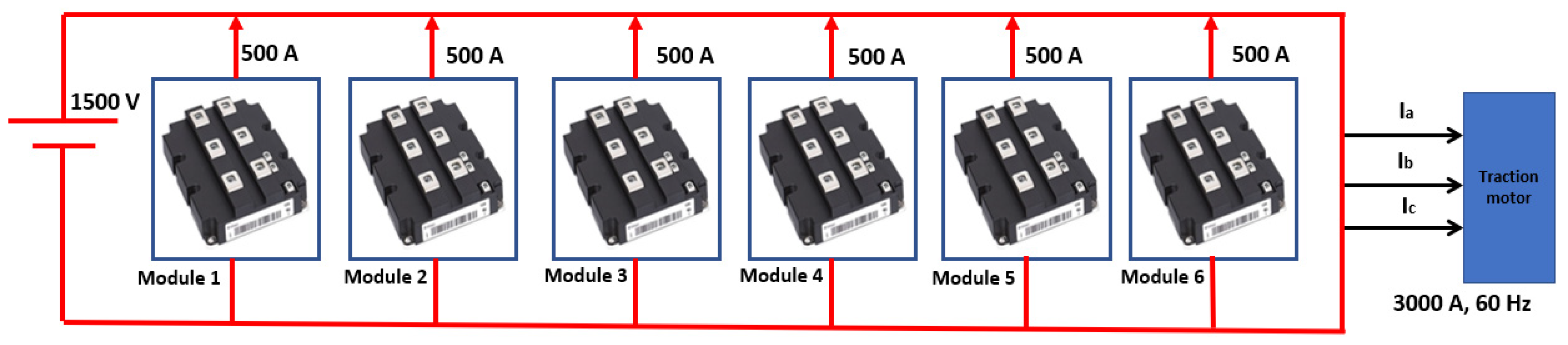
Figure 2.
Schematic circuit of the 3-phase 2-level IGBT module-1.
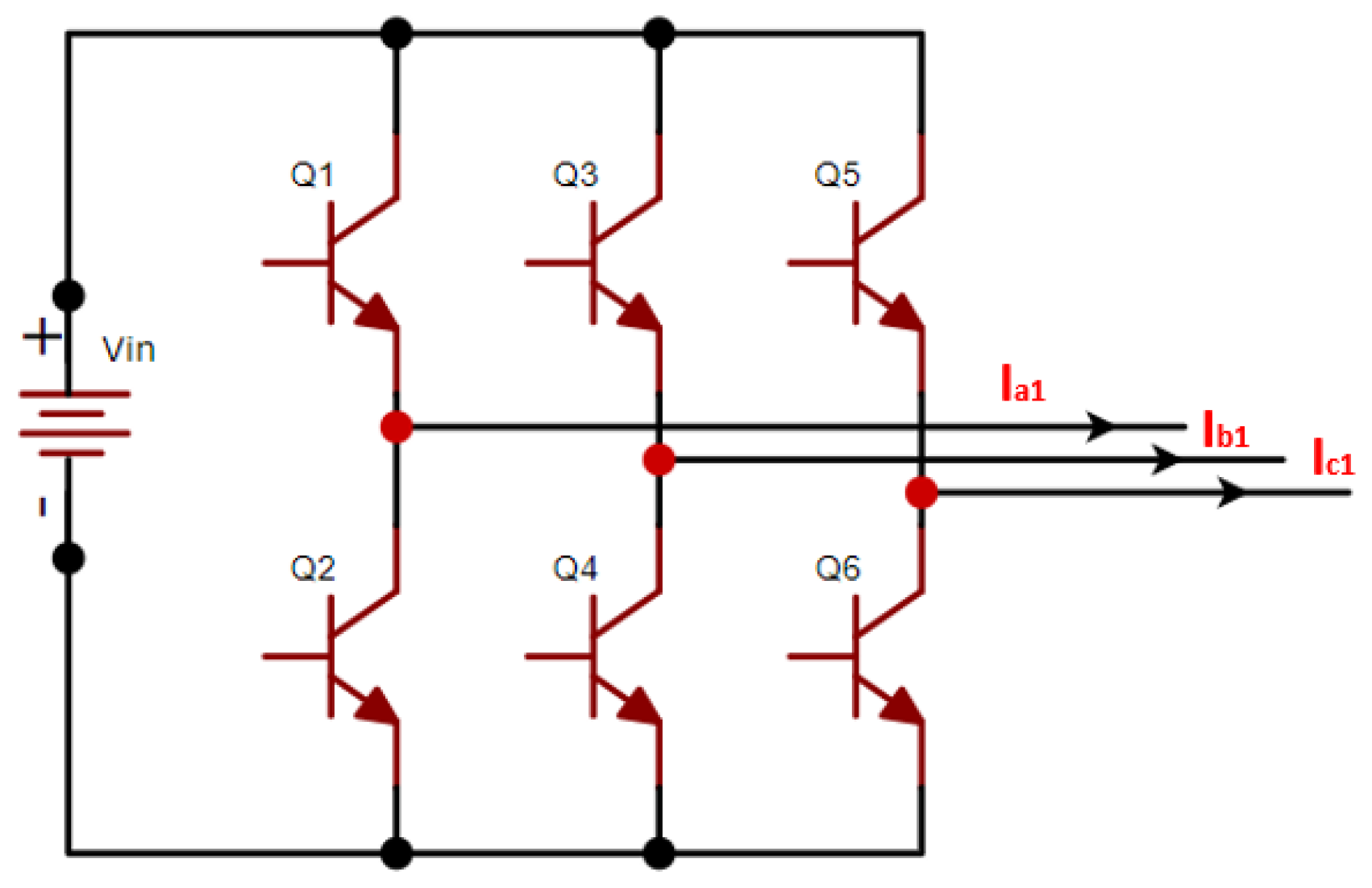
Figure 3.
Steps of the proposed approach for IGBT module temperature estimation.
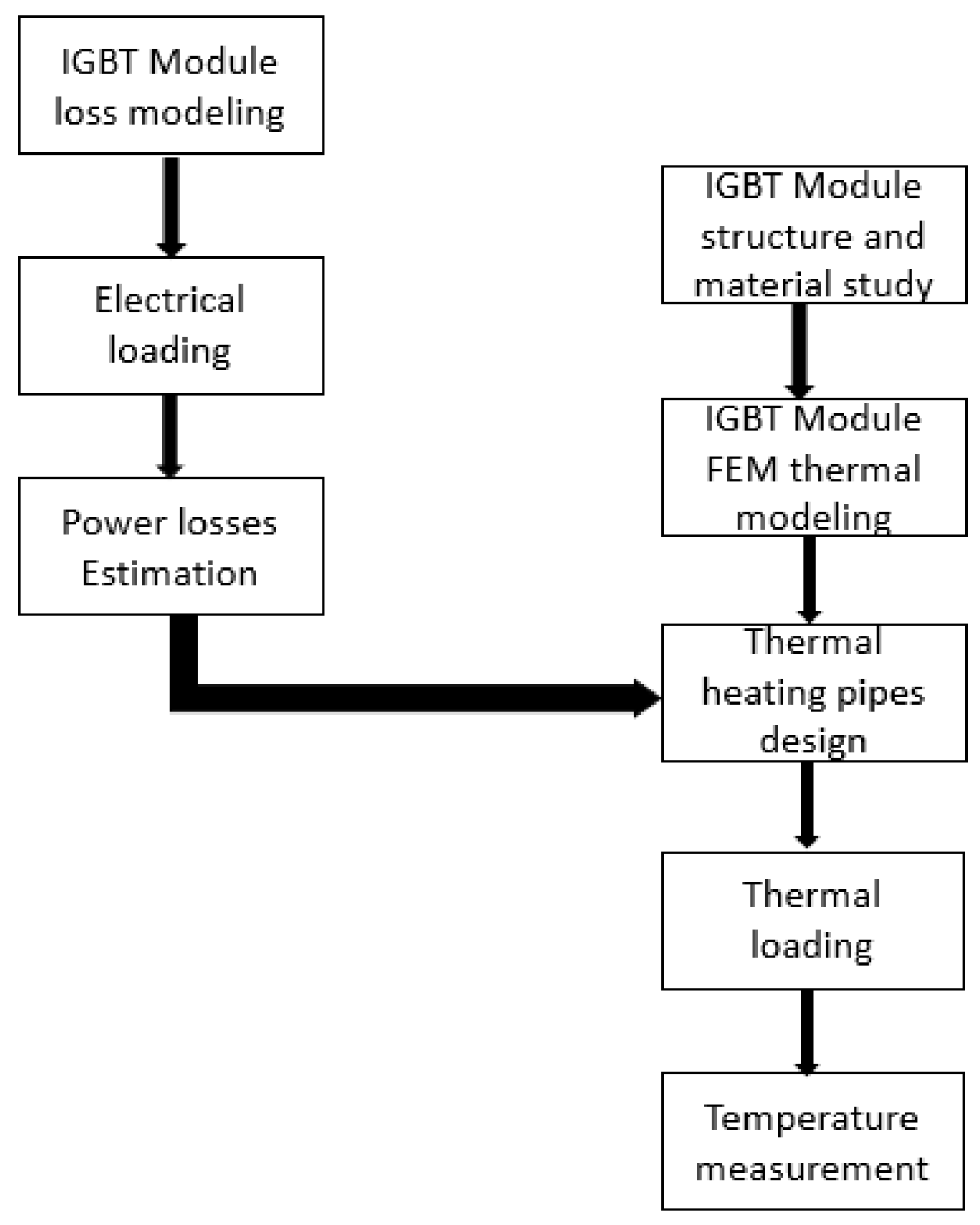
Figure 4.
Circuit schematic phase (leg-A) of the three phase IGBT module 1.

Figure 5.
Equivalent circuits of the transistor and diode chips in conduction state: (a) transistor; (b) diode.
Figure 5.
Equivalent circuits of the transistor and diode chips in conduction state: (a) transistor; (b) diode.

Figure 6.
Transistor and diode chip V-I characteristics of the IGBT module: (a) for transistor; (b) for diode.
Figure 6.
Transistor and diode chip V-I characteristics of the IGBT module: (a) for transistor; (b) for diode.
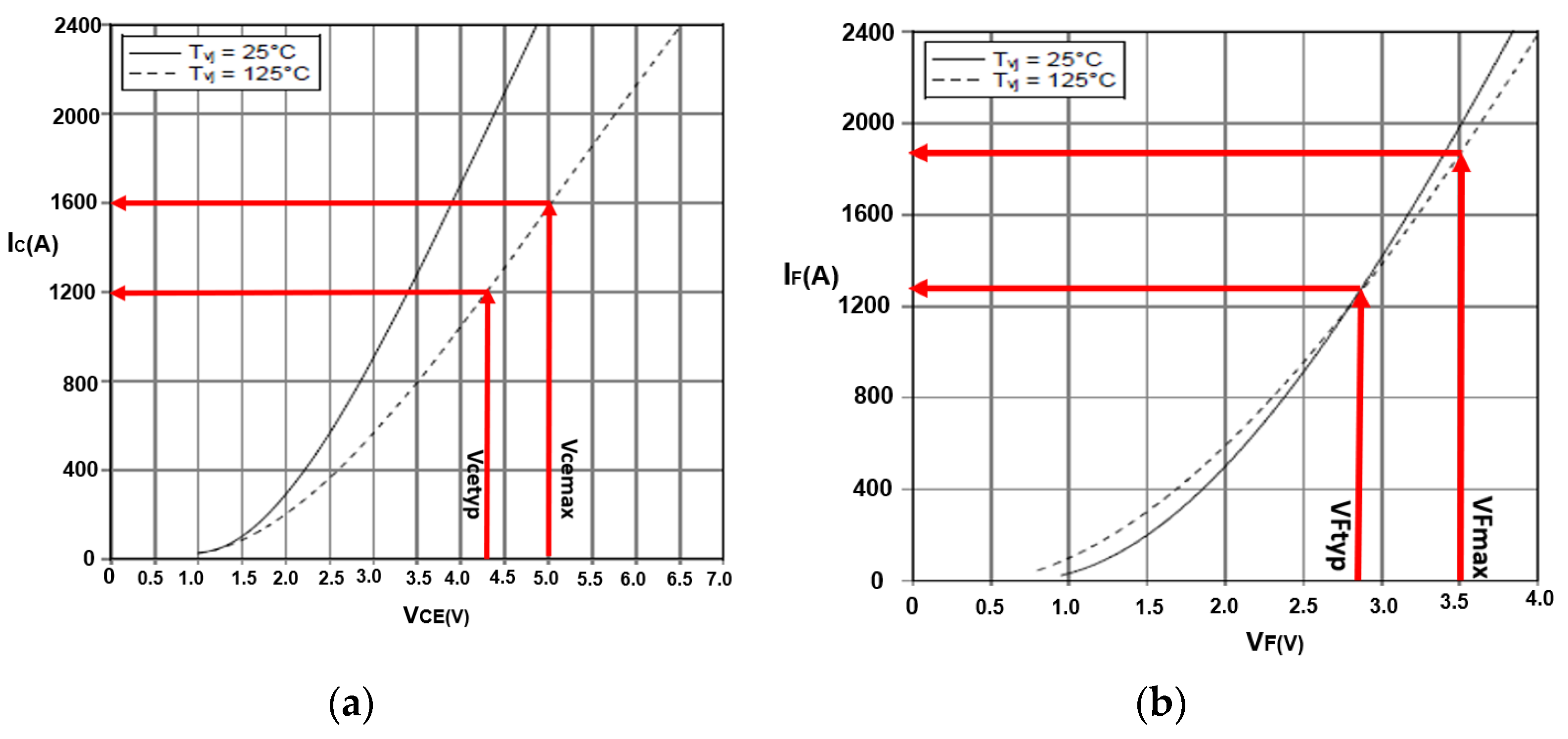
Figure 7.
Carrier and reference voltage waveforms and the PWM signals for the 3-phase 2-level inverter (phase-A) with the dead time control.
Figure 7.
Carrier and reference voltage waveforms and the PWM signals for the 3-phase 2-level inverter (phase-A) with the dead time control.

Figure 8.
The required switching energy at different current for the IGBT module at = 1800 V: (a) for transistor chip, (b) for diode chip.
Figure 8.
The required switching energy at different current for the IGBT module at = 1800 V: (a) for transistor chip, (b) for diode chip.
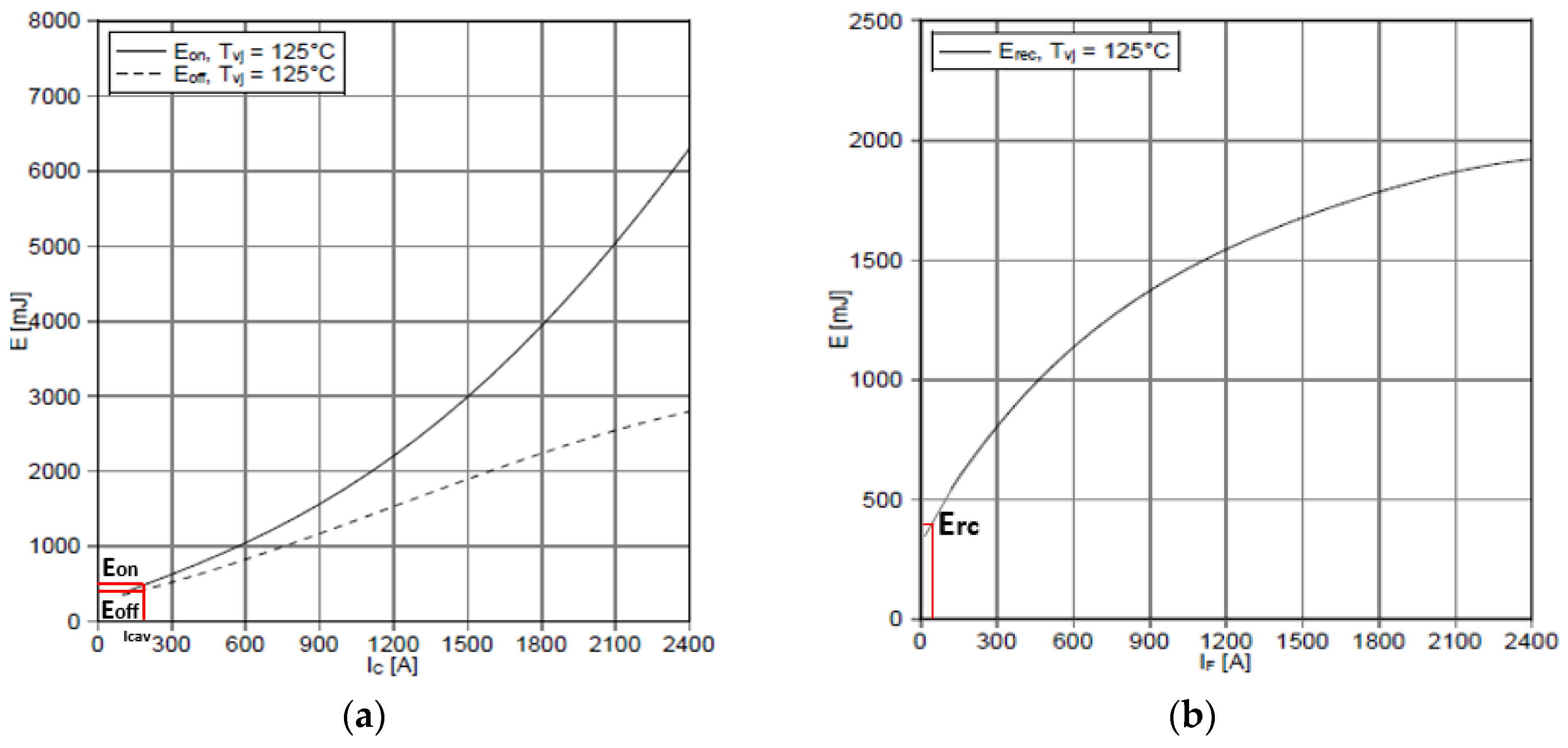
Figure 9.
PSIM model for the loss calculation of the IGBT module.
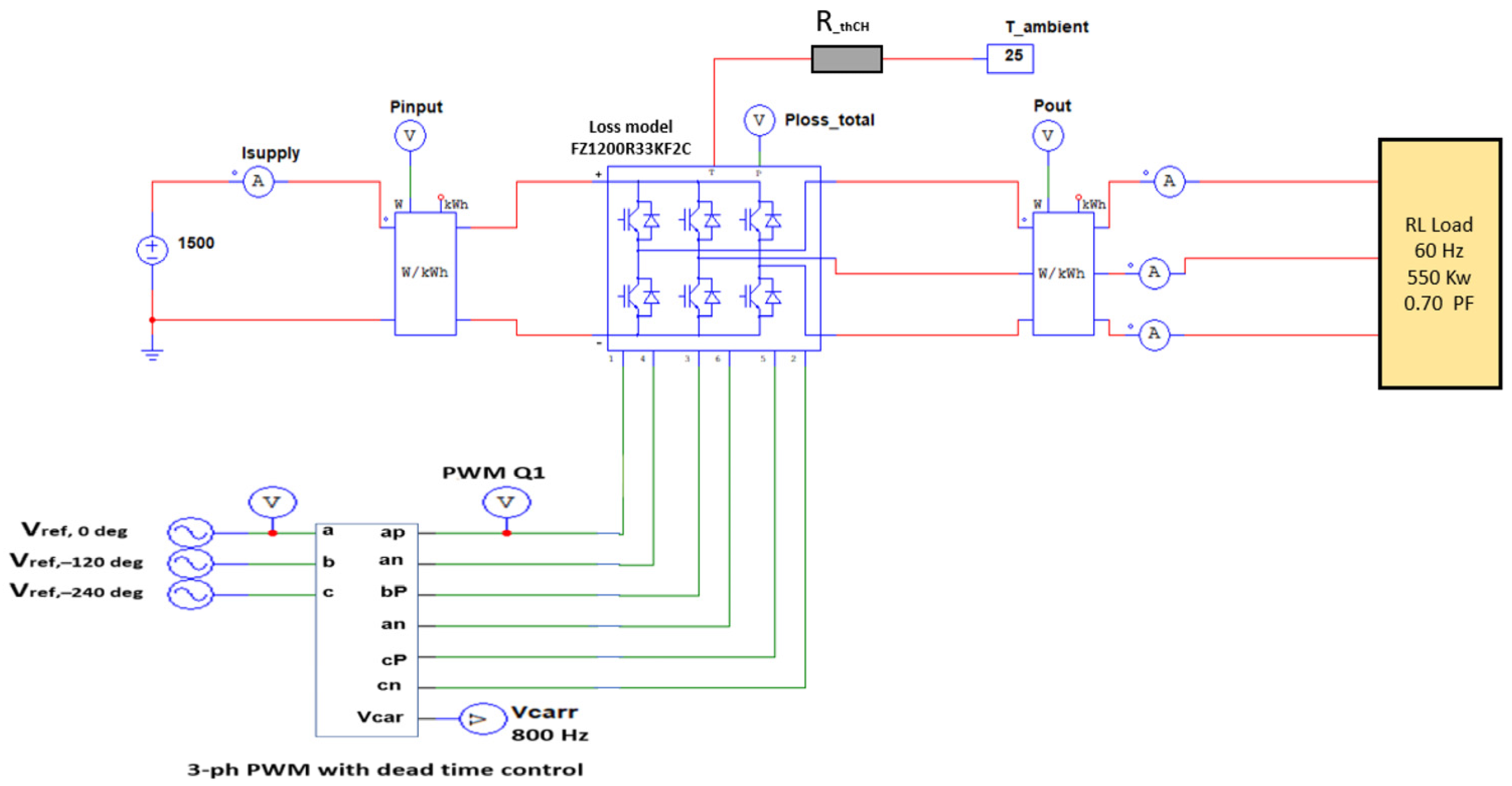
Figure 10.
Three-phase PWM generator with dead time control: (a) voltage comparator; (b) the on/off transition sequence (phase A).
Figure 10.
Three-phase PWM generator with dead time control: (a) voltage comparator; (b) the on/off transition sequence (phase A).
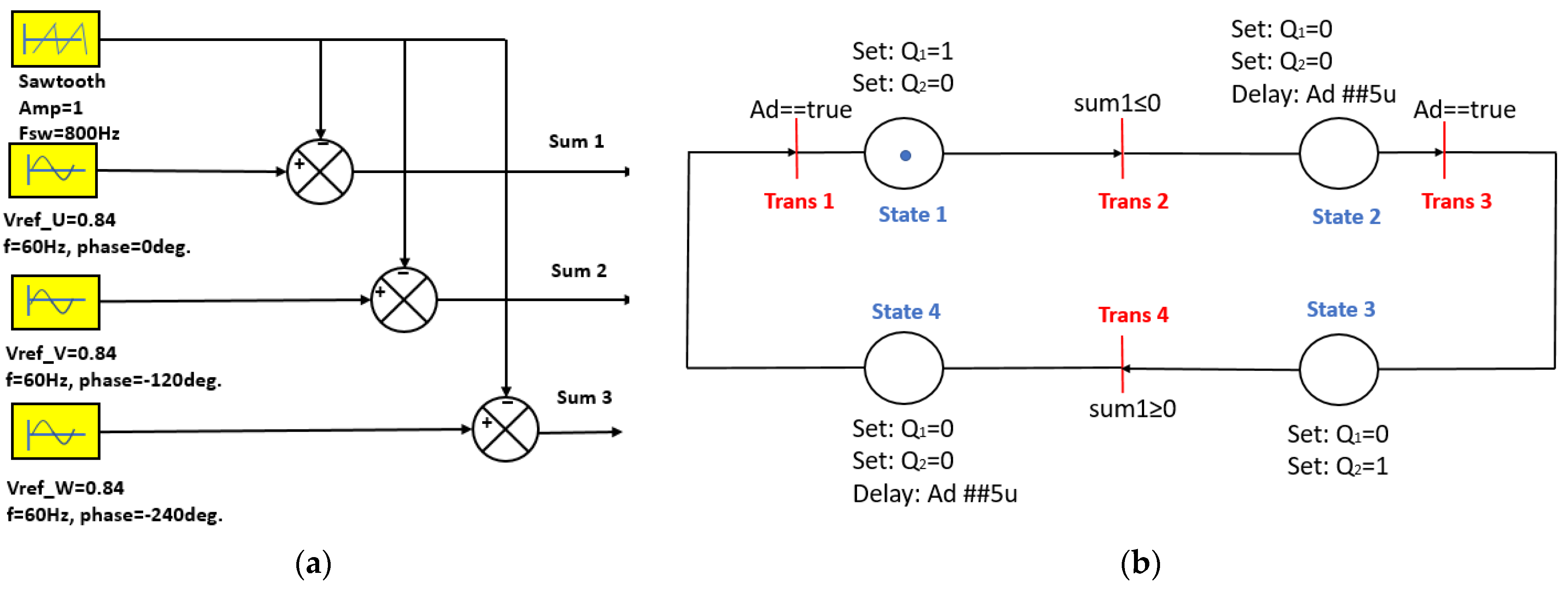
Figure 11.
Voltage comparator waveforms and PWM signals of the three-phase inverter (phase A) with the dead time control.
Figure 11.
Voltage comparator waveforms and PWM signals of the three-phase inverter (phase A) with the dead time control.

Figure 12.
Conduction loss measurement waveforms of the switch Q1 diode (Pcond_Q1_D) and transistor (Pcond_Q1_T).
Figure 12.
Conduction loss measurement waveforms of the switch Q1 diode (Pcond_Q1_D) and transistor (Pcond_Q1_T).
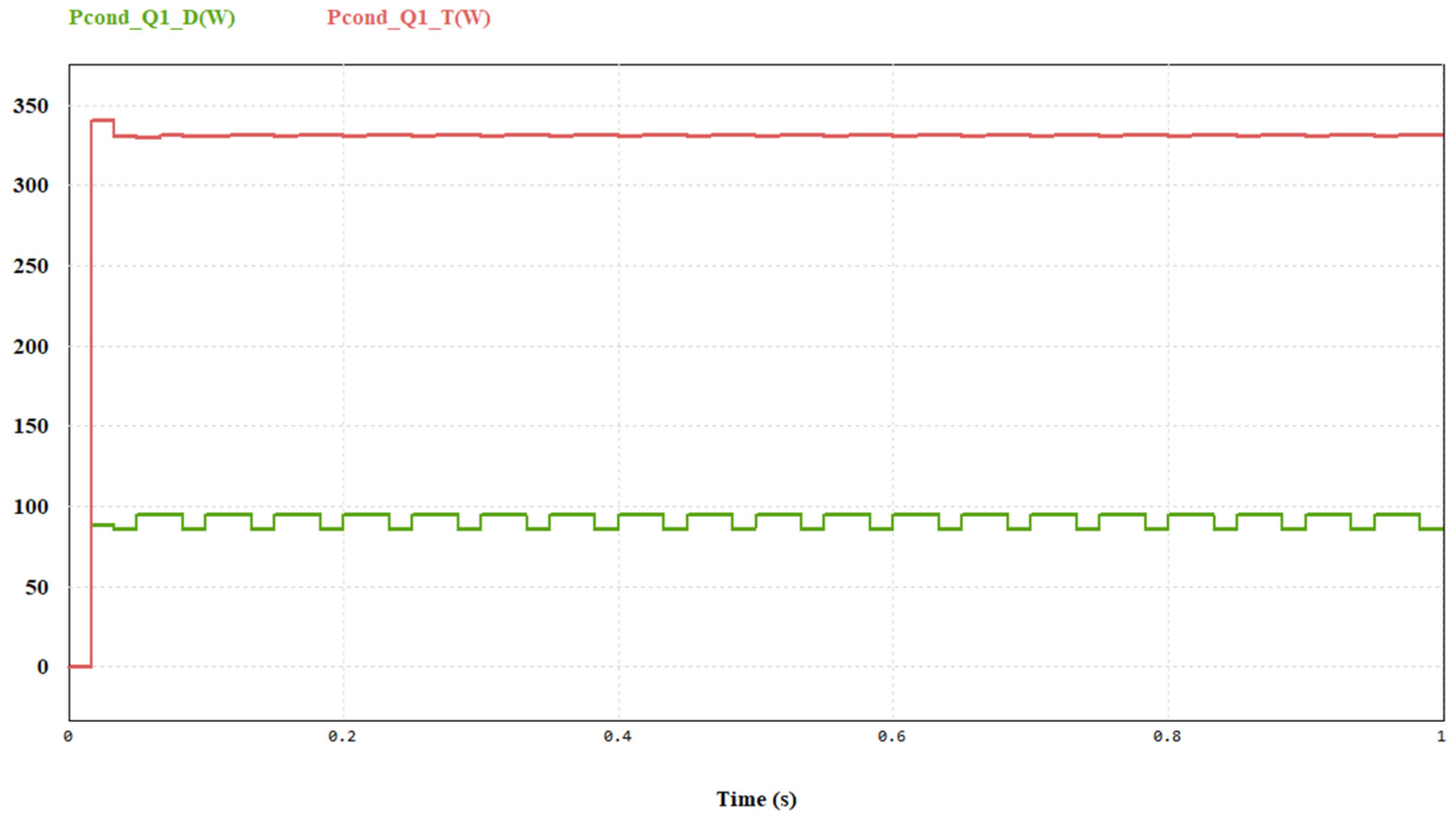
Figure 13.
Switching loss measurement waveforms of the switch Q1 diode (Psw_Q1_D) and transistor (Psw_Q1_T).
Figure 13.
Switching loss measurement waveforms of the switch Q1 diode (Psw_Q1_D) and transistor (Psw_Q1_T).
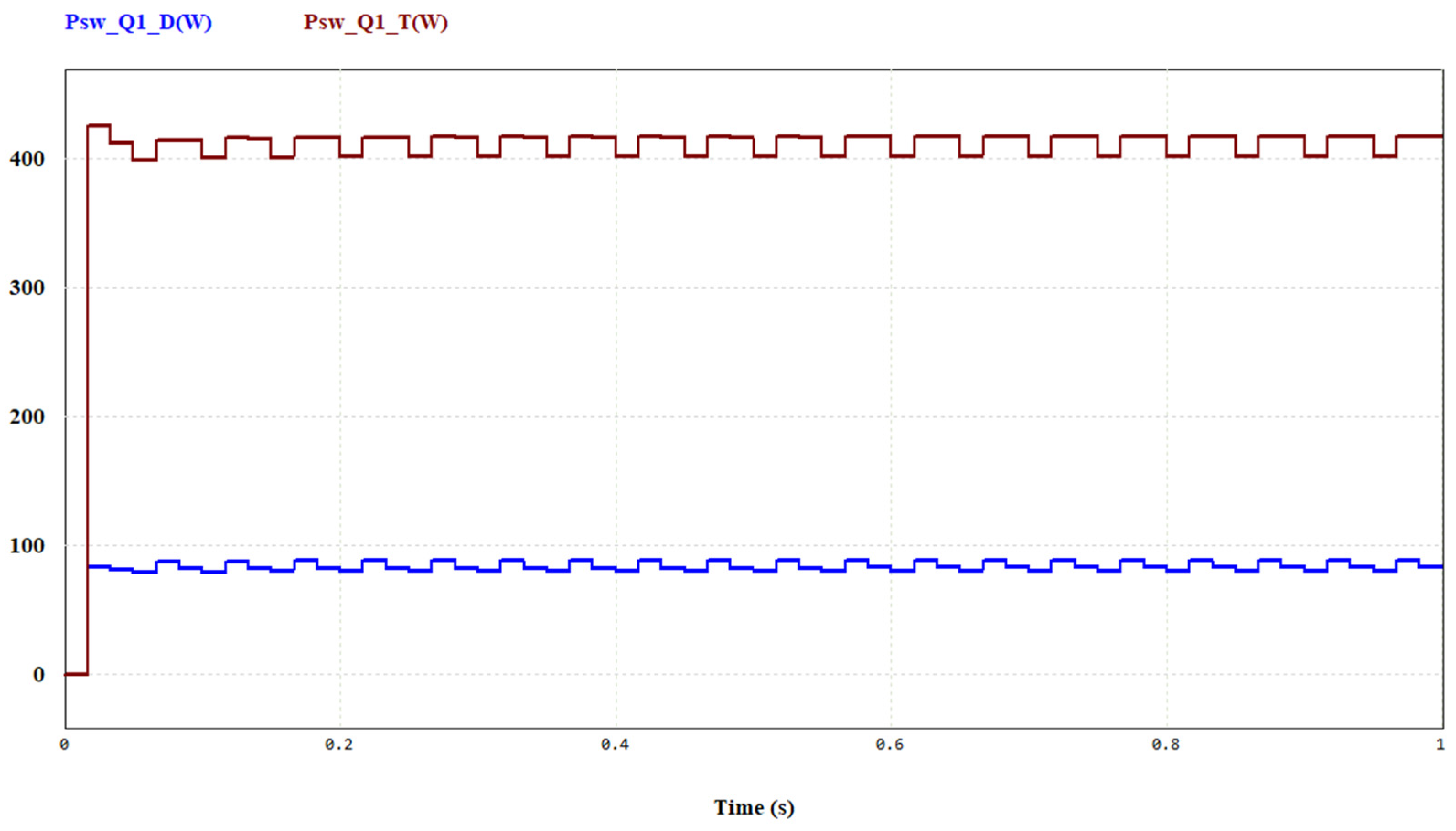
Figure 14.
Total power loss measurement waveforms for the whole IGBT module (Ploss_total) and the switch Q1 (Ploss_Q1).
Figure 14.
Total power loss measurement waveforms for the whole IGBT module (Ploss_total) and the switch Q1 (Ploss_Q1).
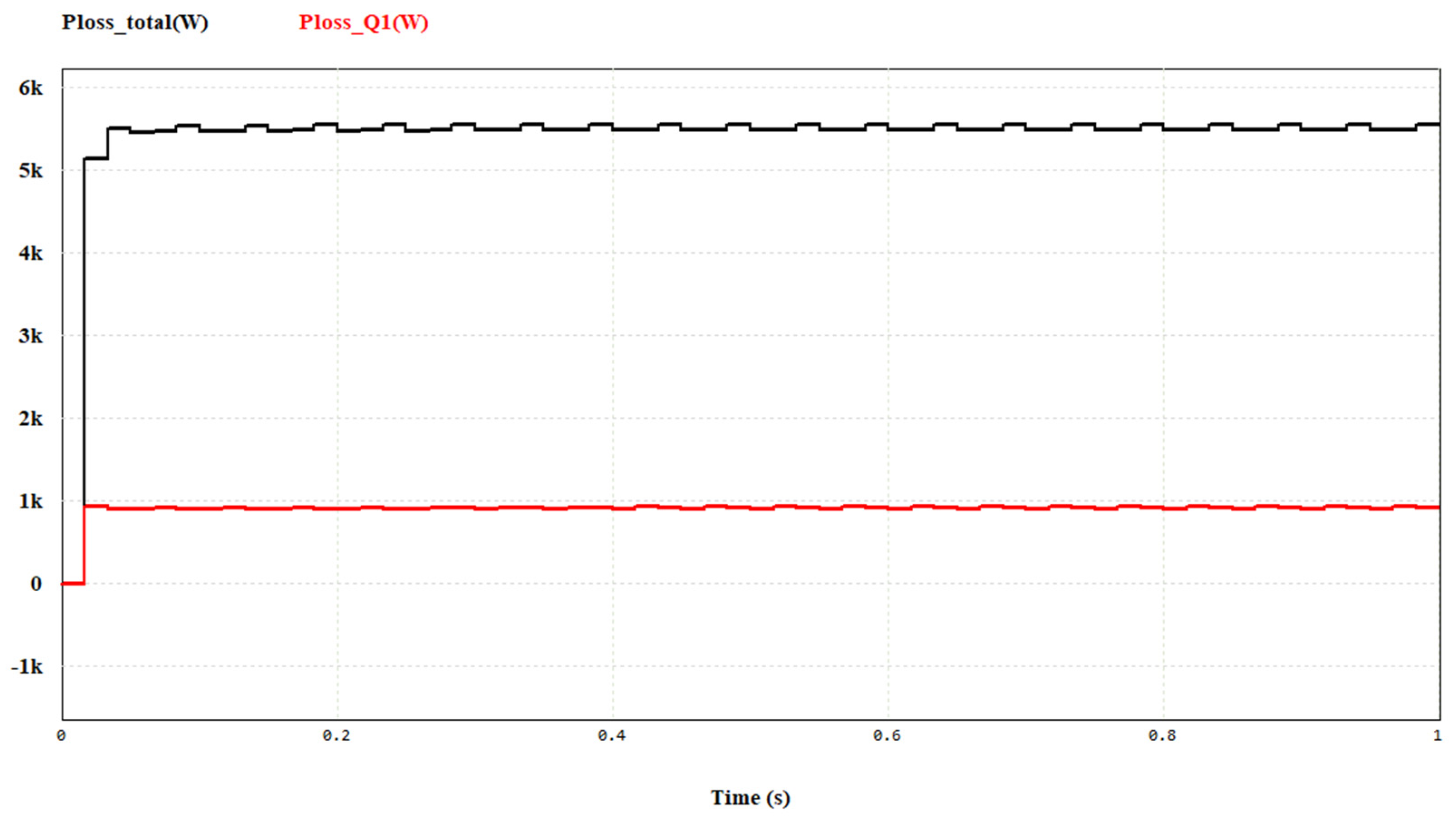
Figure 15.
IGBT module total power losses with different loading condition.
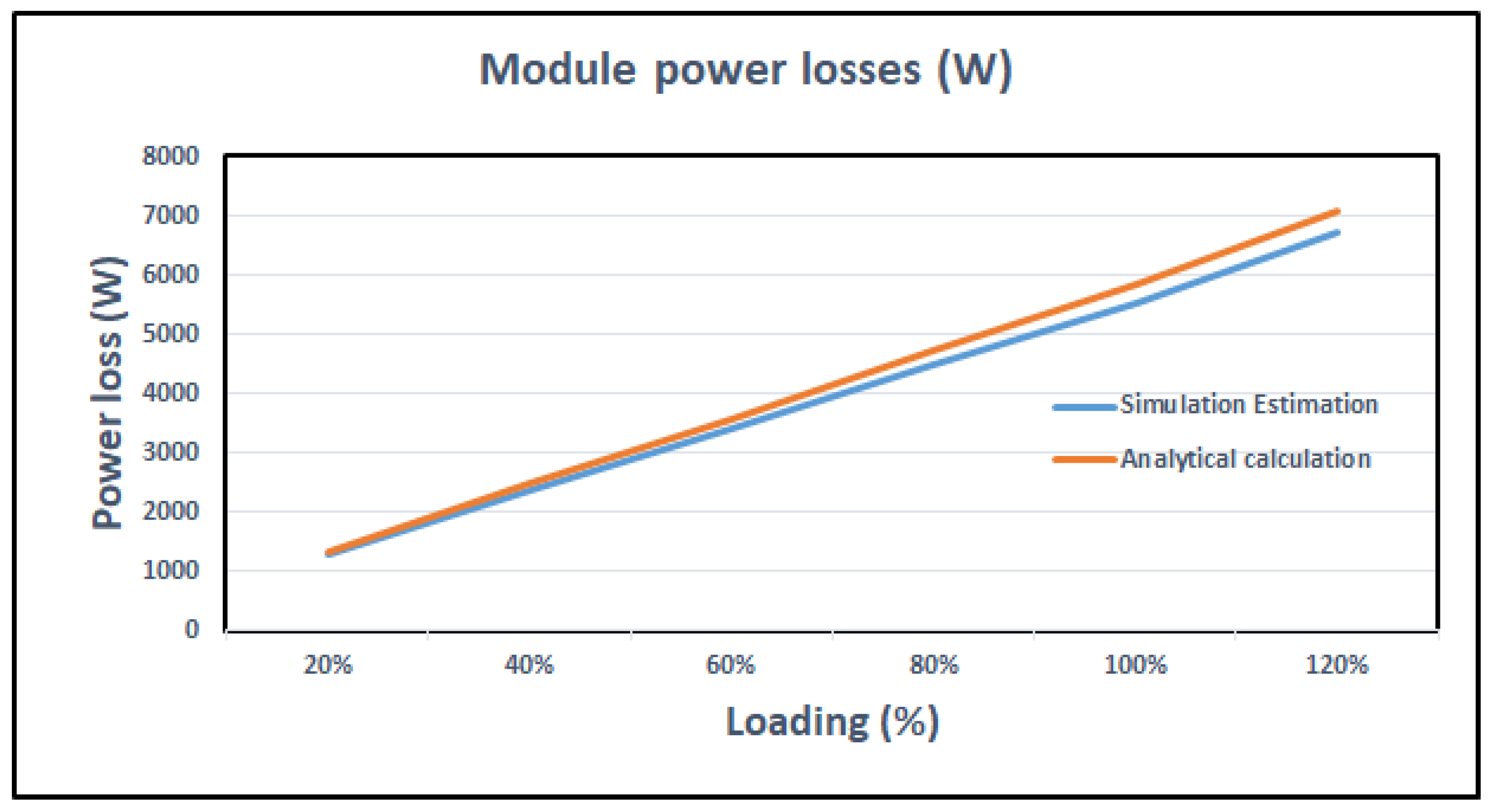
Figure 16.
Structure of a heating pipe system for thermal acceleration test.
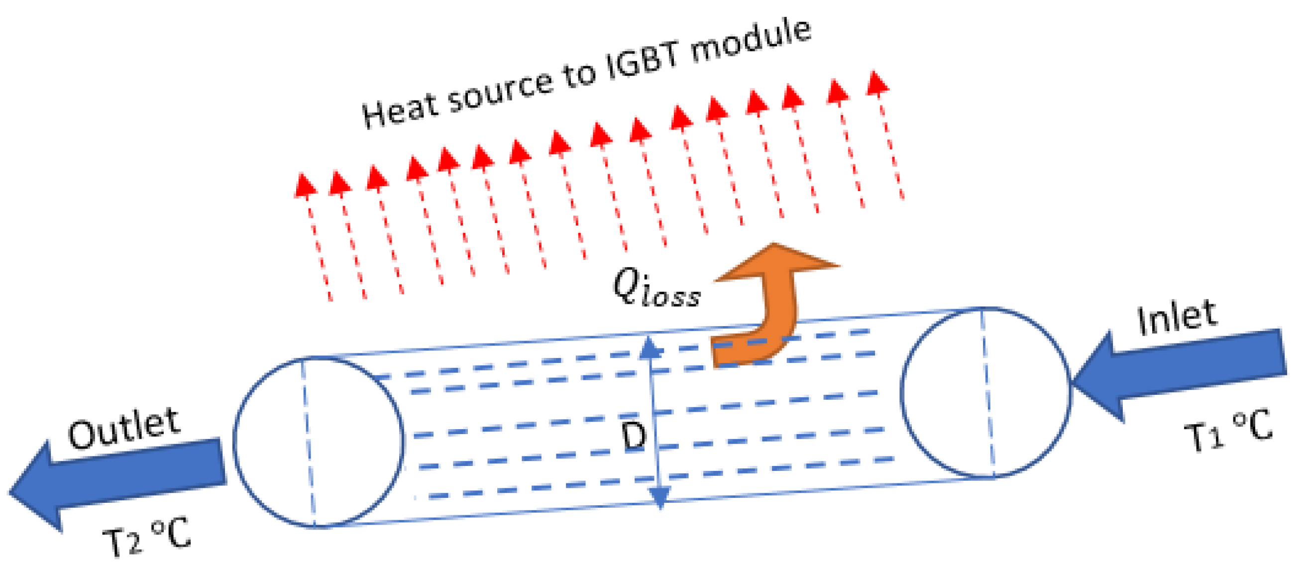
Figure 17.
Operating curves for the designed heat pipe systems: (a) specific heat capacity; (b) water flow.
Figure 17.
Operating curves for the designed heat pipe systems: (a) specific heat capacity; (b) water flow.
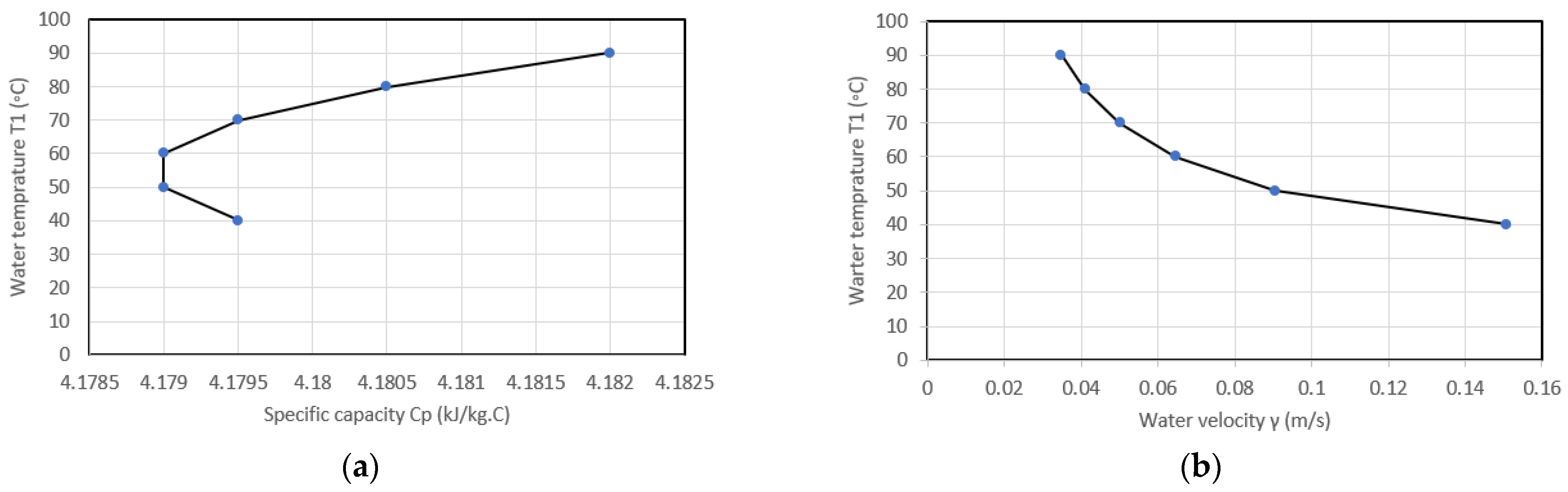
Figure 18.
Construction of the IGBT power module under study.
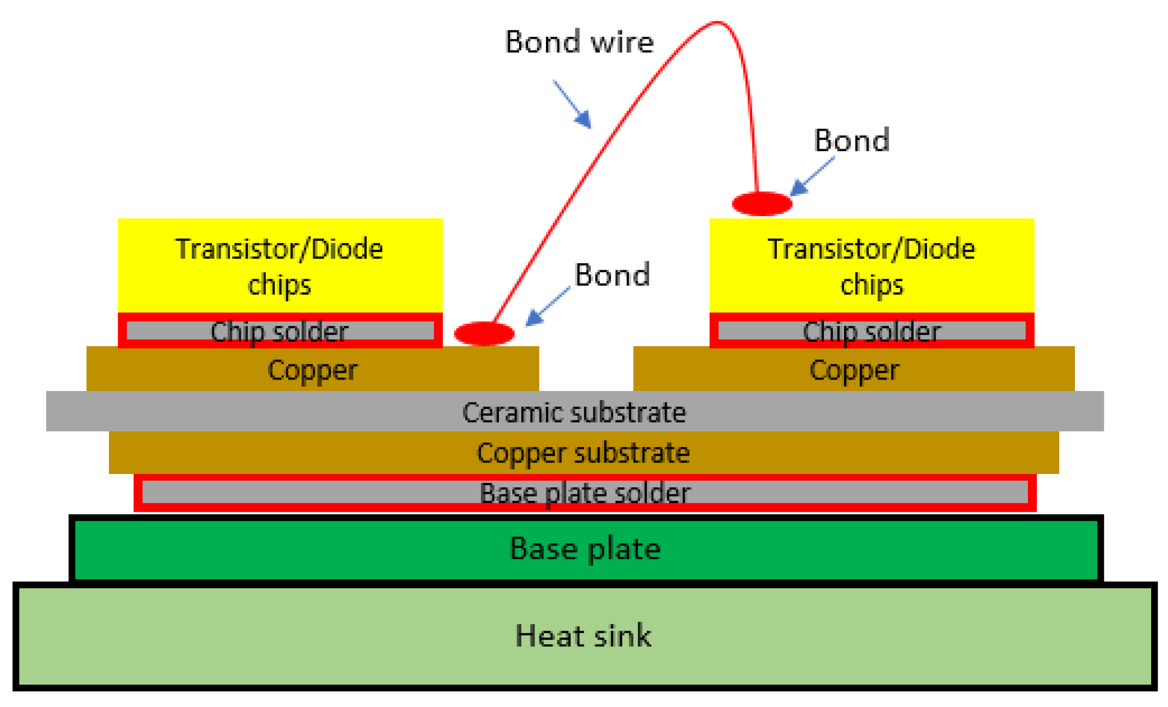
Figure 19.
Modeling of the IGBT module in ANSYS Icepack: (a) 3D view; (b) top view; (c) side view 1; and (d) side view 2.
Figure 19.
Modeling of the IGBT module in ANSYS Icepack: (a) 3D view; (b) top view; (c) side view 1; and (d) side view 2.

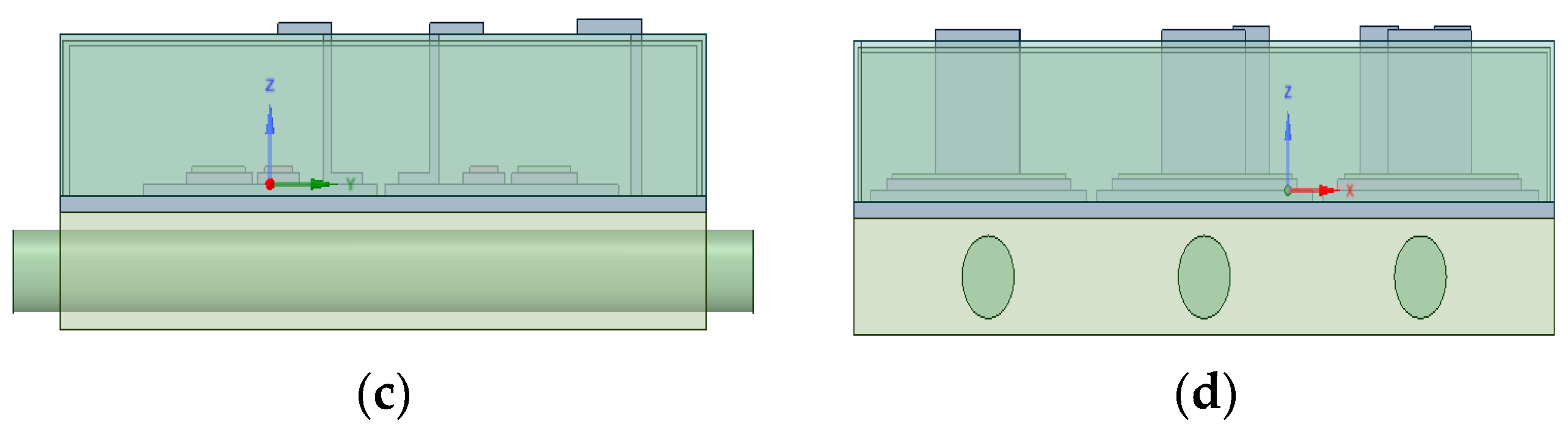
Figure 20.
Boundary conditions of the IGBT module: (a) external boundary condition (cabinet); (b) internal boundary condition (heat pipes).
Figure 20.
Boundary conditions of the IGBT module: (a) external boundary condition (cabinet); (b) internal boundary condition (heat pipes).
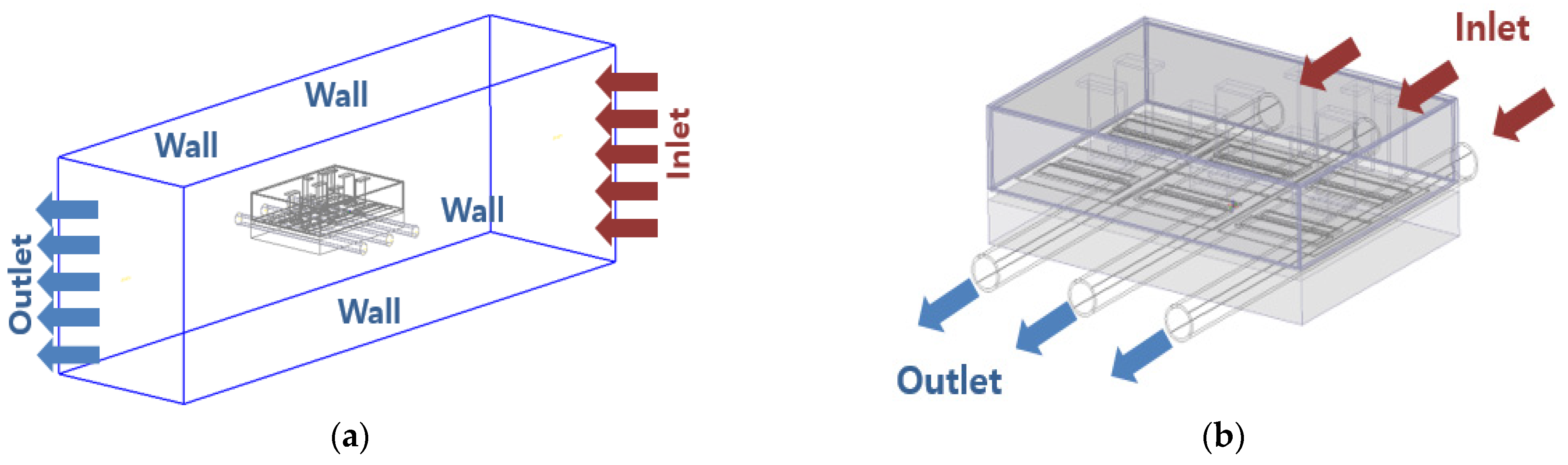
Figure 21.
Solution residuals monitors of the module thermal loading.

Figure 22.
Temperature points monitors of semiconductor chips with iteration numbers.

Figure 23.
Water flow velocity measurement inside the designed heat pipes.

Figure 24.
Airflow shape and velocity measurements in the IGBT module cabinet.
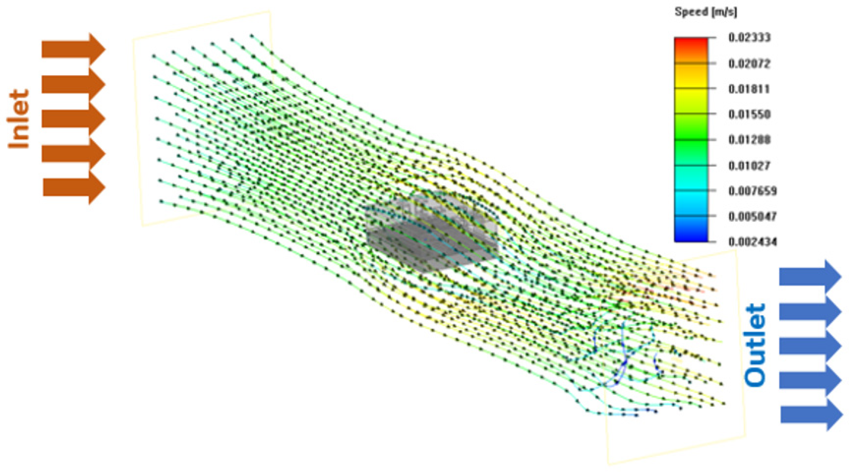
Figure 25.
Three-dimensional view and temperature measurement contour of IGBT module inside the housing.
Figure 25.
Three-dimensional view and temperature measurement contour of IGBT module inside the housing.
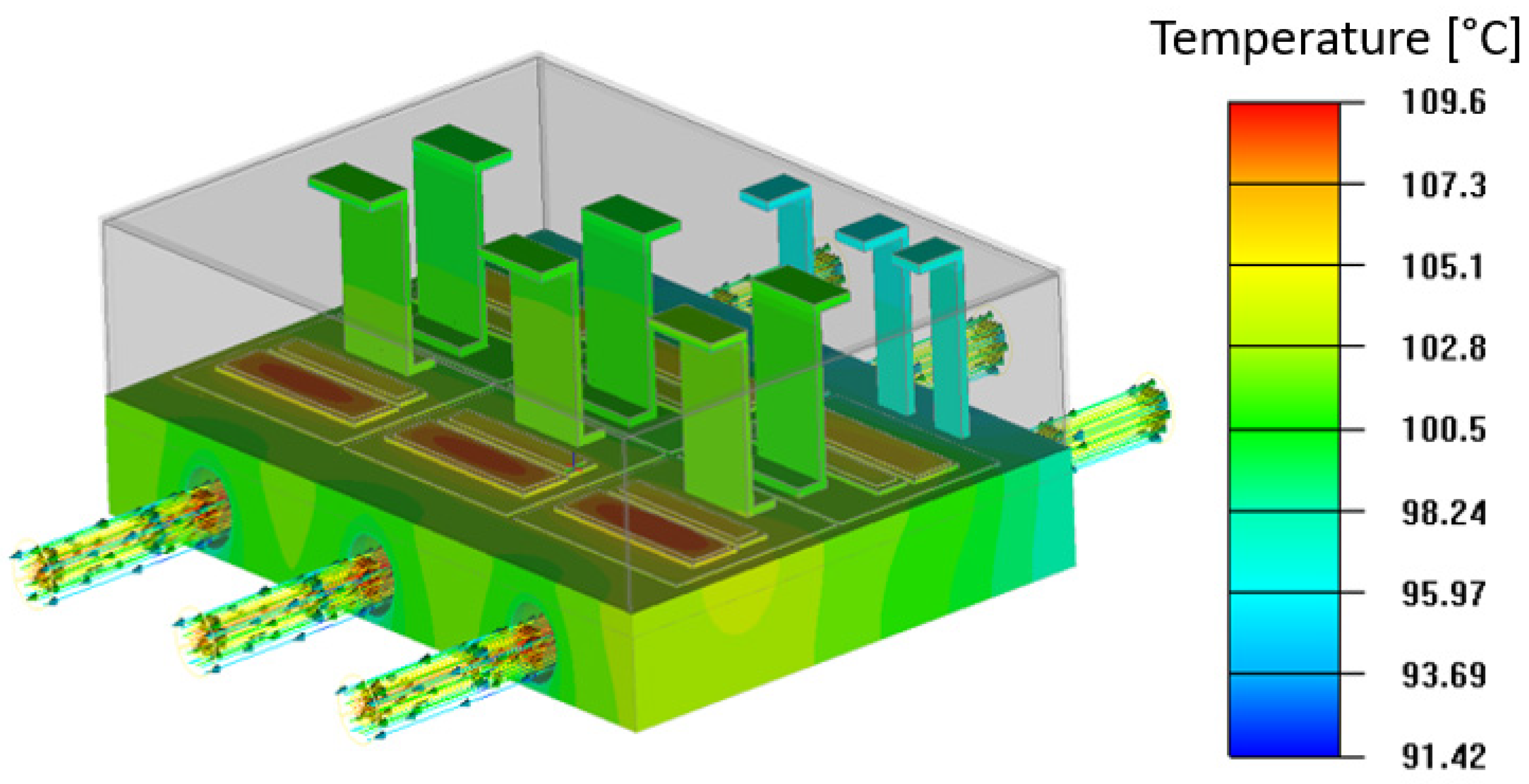
Figure 26.
Positions of module’s semiconductor chips and temperature measurement contour.
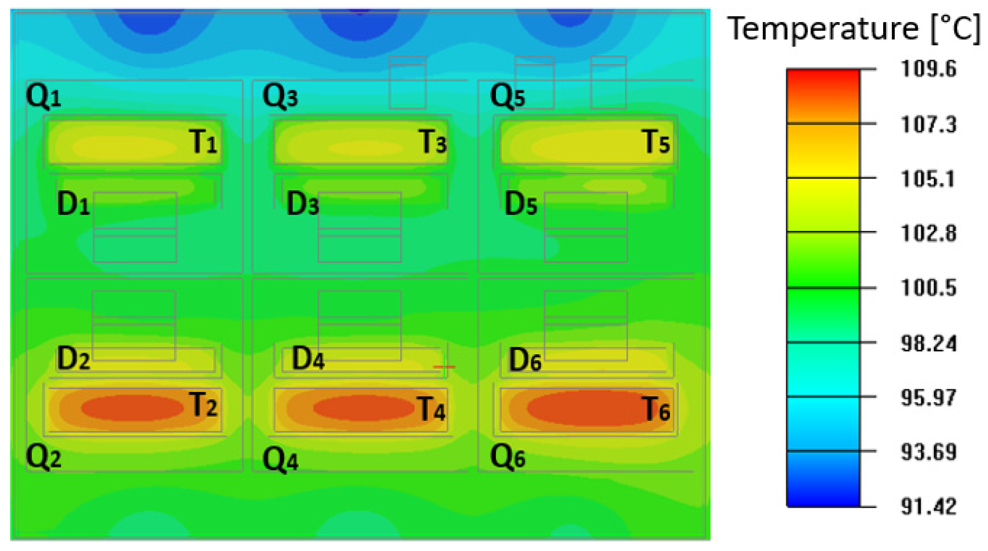
Figure 27.
Temperature measurement of the IGBT module without using the housing.

Table 1.
Design Specifications of the IGBT power module in the target traction inverter.
| Parameter | Value |
|---|---|
| Rated output power (Po) | 550 kW |
| Load power factor (PF) | 0.70 |
| Input DC voltage (Vin) | 1500 V |
| Output load current (Io) | 500 Arms |
| Load frequency (f) | 60 Hz |
| Switching frequency (Fsw) | 800 Hz |
| IGBT module part number | FZ1200R33KF2C |
| Target Max. junction temperature (Tjmax) | 125 °C |
Table 2.
IGBT Module Average Power Losses Calculation and Comparison.
| Losses Term | Average Value (W) | Mismatch% | |
|---|---|---|---|
| Analytical | Simulation | ||
| Pcond_Q1_D | 86.5 | 91.97 | 6.30 |
| Pcond_Q1_T | 352.3 | 331.40 | 5.90 |
| Psw_Q1_D | 91 | 84.06 | 7.60 |
| Psw_Q1_T | 445.67 | 412.08 | 7.50 |
| Ploss_Q1 | 975.67 | 919.51 | 5.75 |
Table 3.
Constituent material properties of the IGBT power module.
| Part | Transistor Chip | Diode Chip | Ceramic Substrate | Copper Substrate | Base Plate | Bus Bar | Housing | Heat Sink | Silicon Fill |
|---|---|---|---|---|---|---|---|---|---|
| Material | Si | Si | Si3N4 | Cu | AlSiC | Cu | Plastic | Al | - |
| Density (Kg/m3) | 2330 | 2330 | 3200 | 8933 | 2960 | 8933 | 1150 | 2700 | - |
| Specific heat (J/Kg-k) | 710 | 710 | 695 | 397 | 740 | 397 | 1600 | 937 | - |
| Conductivity (W/m-k) | 148 | 148 | 80 | 387.4 | 200 | 387.4 | 0.25 | 240 | 0.2 |
Table 4.
IGBT Module Boundary Conditions for Thermal Analysis.
| Boundary Condition | External Boundary Condition | Internal Boundary Condition |
|---|---|---|
| Inlet | Air flow = 0.01 m/s | Water flow = 0.07 m/s |
| Outlet | Opening | Opening |
| Wall | Adiabatic | - |
| Water temperature | - | 60 °C |
Table 5.
IGBT module thermal analysis setup.
| Condition | Value |
|---|---|
| Ambient temperature | 25 °C |
| Variables solved | Flow (water, air), Temperature |
| Analysis time | Steady-State |
| Number of iterations | 100 |
| Flow model | Laminar |
| Air flow | Force convection |
| Generated Mesh | About 5 million used |
| Operating pressure | 1.013 × 10⁵ N/m2 |
Table 6.
Temperature measurements of the module’s semiconductor parts.
| Semiconductor Part | Temp. with Housing (°C) | Temp. without Housing (°C) | |
|---|---|---|---|
| Switch Q1 | T1 | 105.52 | 99.35 |
| D1 | 102.27 | 97.20 | |
| Switch Q2 | T2 | 109.62 | 102.75 |
| D2 | 105.25 | 99.10 | |
| Switch Q3 | T3 | 105.12 | 99.15 |
| D3 | 101.91 | 97.25 | |
| Switch Q4 | T4 | 109.23 | 102.55 |
| D4 | 104.85 | 99.05 | |
| Switch Q5 | T5 | 105.80 | 99.55 |
| D5 | 102.55 | 97.45 | |
| Switch Q6 | T6 | 109.40 | 102.60 |
| D6 | 105.02 | 99.10 | |
Disclaimer/Publisher’s Note: The statements, opinions and data contained in all publications are solely those of the individual author(s) and contributor(s) and not of MDPI and/or the editor(s). MDPI and/or the editor(s) disclaim responsibility for any injury to people or property resulting from any ideas, methods, instructions or products referred to in the content. |
© 2023 by the authors. Licensee MDPI, Basel, Switzerland. This article is an open access article distributed under the terms and conditions of the Creative Commons Attribution (CC BY) license (https://creativecommons.org/licenses/by/4.0/).
Share and Cite
MDPI and ACS Style
Okilly, A.H.; Choi, S.; Kwak, S.; Kim, N.; Lee, J.; Moon, H.; Baek, J. Estimation Technique for IGBT Module Junction Temperature in a High-Power Density Inverter. Machines 2023, 11, 990. https://doi.org/10.3390/machines11110990
AMA Style
Okilly AH, Choi S, Kwak S, Kim N, Lee J, Moon H, Baek J. Estimation Technique for IGBT Module Junction Temperature in a High-Power Density Inverter. Machines. 2023; 11(11):990. https://doi.org/10.3390/machines11110990
Chicago/Turabian StyleOkilly, Ahmed H., Seungdeog Choi, Sangshin Kwak, Namhun Kim, Jonghyuk Lee, Hyoungjun Moon, and Jeihoon Baek. 2023. "Estimation Technique for IGBT Module Junction Temperature in a High-Power Density Inverter" Machines 11, no. 11: 990. https://doi.org/10.3390/machines11110990
Note that from the first issue of 2016, this journal uses article numbers instead of page numbers. See further details here.