Article

Analysis of the Effects of Parameters on the Performance of Resonators Based on a ZnO/SiO2/Diamond Structure

National Key Laboratory for Electronic Measurement Technology, Key Laboratory of Instrumentation Science and Dynamic Measurement, Ministry of Education, North University of China, Taiyuan 030051, China
*
Author to whom correspondence should be addressed.
Appl. Sci. 2024, 14(2), 874; https://doi.org/10.3390/app14020874
Submission received: 22 December 2023 / Revised: 15 January 2024 / Accepted: 17 January 2024 / Published: 19 January 2024

Abstract

:
With the development of communications technology, surface acoustic wave (SAW) and bulk acoustic wave (BAW) devices have become hotspots of the competitive research in the frequency band above GHz. It imposes higher requirements on the operating frequency, temperature coefficient of frequency (TCF), and electromechanical coupling coefficient (k2) of SAW devices. In this work, we reported on a novel ZnO/SiO2/diamond-layered resonator structure and systematically investigated its propagation characteristics by using finite element methods. A comparative study and analysis of k2 and acoustic velocity (vp) for both the excited Rayleigh mode and the Sezawa mode were conducted. By selecting the appropriate ZnO piezoelectric film, SiO2, and electrode thickness, the Sezawa mode was chosen as the main mode, effectively improving both k2 and vp. It was observed that the k2 of the Sezawa mode is 7.5 times that of the excited Rayleigh mode and nearly 5 times that of piezoelectric single-crystal ZnO; vp is 1.7 times that of the excited Rayleigh mode and nearly 1.5 times that of piezoelectric single-crystal ZnO. Furthermore, the proposed multilayer structure achieves a TCF close to 0 while maintaining a substantial k2. In practical applications, increasing the thickness of SiO2 can compensate for the device’s TCF reduction caused by the interdigital transducer (IDT). Finally, this study explored the impact of increasing the aperture width and IDT pairs on the performance of the single-port resonator, revealing the changing patterns of quality factor (Q) values. The results reported here show that the structure has great promise for the fabrication of high-frequency and low-TCF SAW devices.

1. Introduction

With the wide application of SAW devices in the field of fifth-generation (5G) mobile communications [1,2], the requirements for their performance are increasing. They are gradually developing towards high frequenc, large electromechanical coupling coefficients, and high-temperature stability [3,4,5]. There are three main approaches to the realization of high-frequency devices: (1) By improving the photolithography precision. The SAW device operating frequency is related to the electrode width of the IDT [6]. However, high-precision lithography is expensive and the electrode is too fine for the device power tolerance to be tested [7]. (2) By selecting waves with higher sound speeds, such as Rayleigh wave < SH wave < Sezawa wave [8]. (3) With the development of piezoelectric thin-film technology, by selecting the advantages of multilayer dielectrics composed of different materials. It is possible to improve the phase velocity and electromechanical coupling coefficients of SAW devices, as well as the temperature stability, which reduces the photolithographic accuracy required for device production [9,10].
Devices of common piezoelectric materials, such as LiNbO3 and LiTaO3, are difficult to integrate on chip with other circuits or microelectromechanical systems (MEMS) devices due to the limitation of the cut angle, and the range of applications is greatly restricted [11]. The SAW devices based on piezoelectric thin films using ZnO and AlN can be fabricated on a variety of substrates, which makes them very suitable for integration with other parts of the system, and they have high research value in the fabrication of high-frequency SAW devices [12,13]. ZnO piezoelectric films have the advantages of favorable piezoelectricity, easy preparation, low insertion loss, etc. Relevant studies have shown that ZnO piezoelectric films have a high degree of orientation in any substrate deposition, which is because ZnO crystals will always grow in the direction of the lowest free energy at the surface, and thus, ZnO piezoelectric films have better consistency [14,15,16]. Among various substrates, diamond substrates have extremely high sound velocity, which is conducive to the production of high-frequency SAW devices [17]. In addition, the thermal conductivity of a diamond is very high; thus, it can effectively transfer and disperse heat, thereby improving the power tolerance of SAW devices.
Reference [18] investigated the properties of acoustic surface waves propagating in structures of ZnO/Si and ZnO/AlN/Si. The numerical analysis involved examining the vp, k2, and TCF of the first two mode frequencies of the SAWs in the ZnO/Si structure. Then, the results of the analysis were compared to the experimental data. Reference [19] achieved a k2 of 6.6% for the Rayleigh mode by employing embedded electrodes based on the ZnO/SiO2/Al2O3 structure, which is feasible for the fabrication of a broadband acoustic surface wave device, but the selected Rayleigh wave is only available for a low vp of 2960 m/s. The propagation characteristics of acoustic surface waves in ZnO film/R-sapphire structures were investigated in reference [20]. The Rayleigh wave was found to have a large k2 of 4.95% and a phase velocity of 5300 m/s in ZnO film/R-sapphire substrates, but the TCF of their devices was not satisfactory.
In order to improve the operating frequency, bandwidth, and temperature stability of piezoelectric single-crystal ZnO SAW devices, in this work, we introduced a novel ZnO/SiO2/diamond-layered structure in the design of SAW devices. A 3D model was established using the finite element method (FEM). The eigenfrequency solving and frequency domain simulation were carried out to obtain the effects of ZnO piezoelectric thin film, SiO2 temperature complementary layer, and electrode thickness on the performance of Rayleigh and Sezawa waves. Then, a performance comparison between Rayleigh and Sezawa waves was made. The simulation results show that the Sezawa wave as the main mode in this structure has obvious advantages over the Rayleigh wave in terms of k2, vp, etc. By simulating the admittance of the single-port resonator to obtain the Q-value change rule, this paper provides a feasible solution in terms of the design and optimization of high-frequency SAW devices.

2. Simulation Principle and Model Structure

2.1. Model Structure

In this study, COMSOL 6.1 software was used to model and simulate the designed multilayer structures. Figure 1a shows a schematic of a 3D unit cycle of an IDT/ZnO/SiO2/diamond structure. The terms h1, h2, and h3 denote the thicknesses of the ZnO piezoelectric film, the temperature complementary layer, and the IDT electrodes whose material is Al. The SAW device’s wavelength (λ) is 2 μm. Since the majority of the energy of the SAW device is limited to one wavelength, the diamond substrate is set to a fixed value of 4 λ, and the thickness of the perfectly matched layer (PML) at the bottom is 1 λ, which not only reduces the model size but also avoids the boundary reflection at the bottom [21]. This work applies a terminal rated at 1 V to one of the electrodes and grounds the other. The distance between each electrode in the model is 0.25 λ, and the metallization rate (MR) is designed to be 50%. In this work, the model has a period of 1 λ along the x direction and the thickness is set to 0.2 λ along the y direction. For the design of the boundary conditions of the model, it is assumed that the infinite-length plate is modeled with periodic boundary conditions in both the x and y directions and that the bottom of the PML is fixed. Figure 1b shows a schematic of meshing of the model in COMSOL with a mesh size of λ/8.

2.2. Model’s Material Parameters

Table 1 lists the various material parameters utilized in the simulation model seen in Figure 1, where the tangential direction of the ZnO piezoelectric film is set to (0, 0, 0) by the rotational coordinate system in COMSOL, and all the studies in this paper are centered around this tangential ZnO piezoelectric film [22]. The model in this study utilizes materials such as Al, ZnO, diamond, and SiO2. Table 1 presents the primary parameters of these materials, which were obtained from the COMSOL software database [23,24,25,26].

3. Simulation Performance Analysis

3.1. Modal Analysis

The theory governing the SAW resonator postulates that the SAW induced by the IDT can be comprehended as a combination of multiple pairs of IDT excitation signals. Consequently, the link between the inherent frequency of the SAW and λ may be ascertained [27]:
f 0 = v p λ
where f0 is the center frequency of the SAW device and vp is the propagation speed of the sound wave. The propagation velocity vp of the SAW can be found by using the following formula:
v p = λ f s c + + f s c 2
where fsc+ and fsc− are the symmetric and antisymmetric mode frequencies of the SAW, respectively [28].
The k2 value for the device’s electromechanical coupling can be computed by using the following equation [29]:
k 2 = π 2 ( 4 f sc + f sc ) f sc +
The TCF can be computed by substituting the parameters T = 0 °C and T0 = 25 °C into the given equation and calculating the resulting vp [30]:
T C F = 1 T T 0 v T v T 0 v T 0
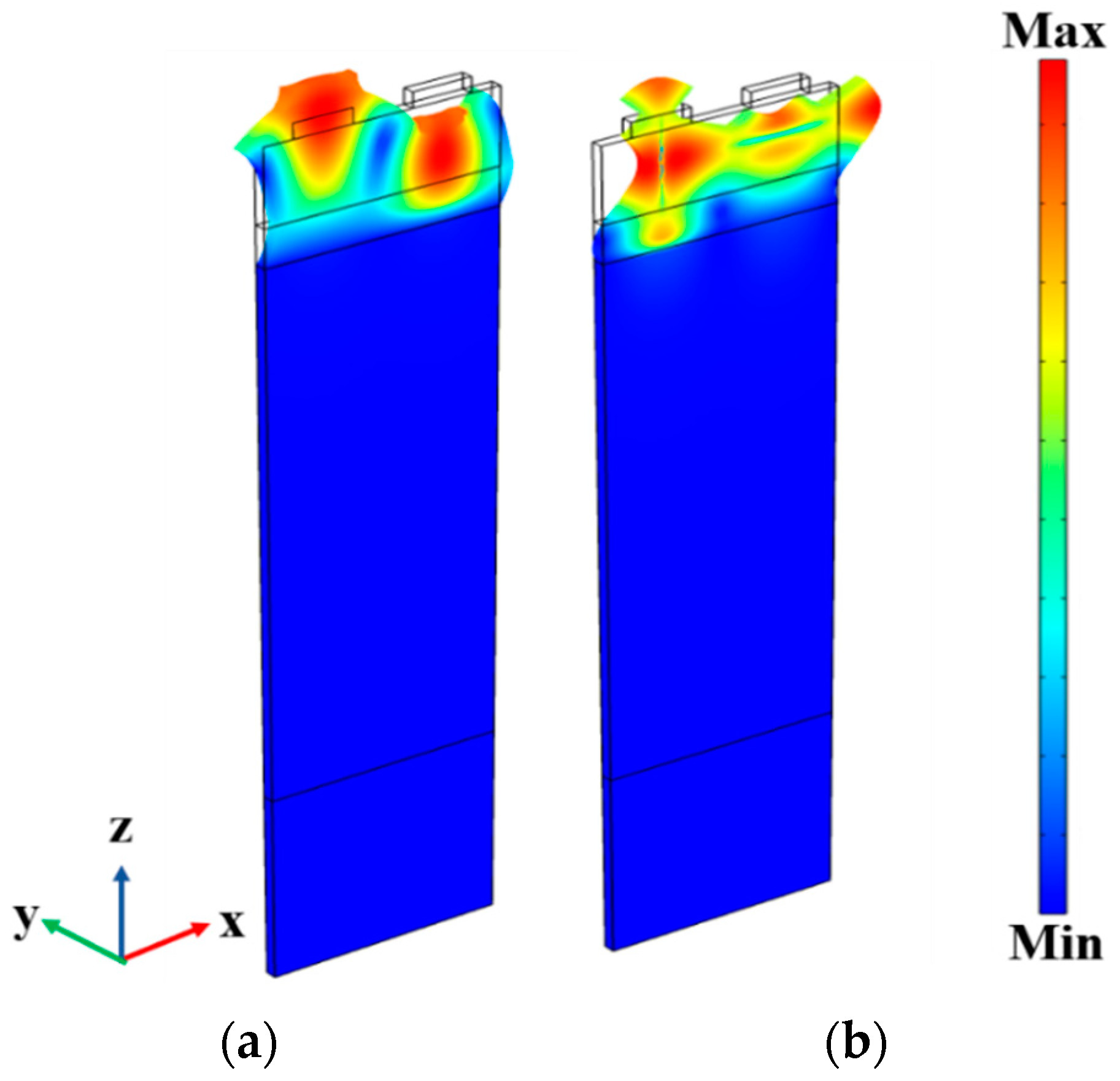
Due to the higher sound velocity of the diamond substrate compared to that of the ZnO piezoelectric film, the Rayleigh and Sezawa modes coexist in a single multilayer structure [17]. Firstly, a ZnO/SiO2/diamond model is developed to characterize the propagation of acoustic waves in this layered structure. The effectiveness of SAW devices featuring multilayer film designs depends on multiple factors, including the thickness of the piezoelectric film and IDT, the construction of the transducer, and the characteristics of the piezoelectric material. In a layered system in which the SAW is a dispersive wave, the ratio of the acoustic wave’s wavelength to the thickness of the various films, including the piezoelectric film, determines the acoustic parameters’ dispersive characterization. As a result, optimizing the geometric parameters can significantly enhance the SAW device’s performance. Following that, by using the method of controlling variables, specifically when the thickness of the Al electrode can be considered negligible, this study investigates the influence of the normalized thickness variations (h1/λ, h2/λ) of the ZnO film and SiO2 layer on the vp and k2 of the Rayleigh and Sezawa modes in this structure. Next, the effect of IDT thickness on the acoustic performance of the Rayleigh and Sezawa modes when h1/λ = 0.4 and h2/λ = 0.2 is investigated, and the modal analyses of the Rayleigh and Sezawa modes are conducted after determining the parameters, as seen in Figure 2, which shows the resonance modes of the Rayleigh and Sezawa waves.

3.2. Piezoelectric and SiO2 Film Effects on the Properties of SAW Propagation

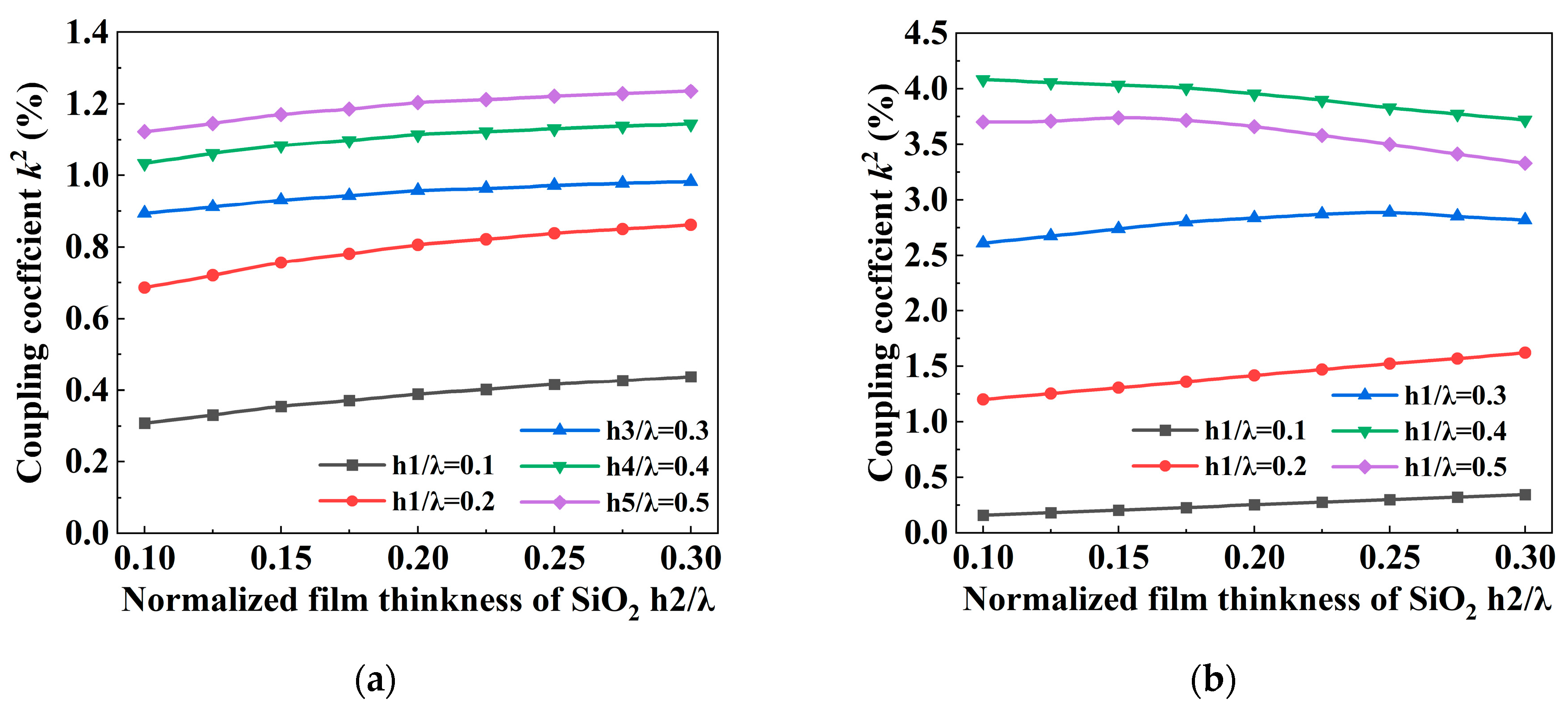
To investigate the effects of ZnO and SiO2 films on the properties of SAW propagation, the k2 curves of the Rayleigh and Sezawa waves in the ZnO/SiO2/diamond structure are shown in Figure 3. Here, the thickness of the Al electrode is negligible, where the normalized film h1/λ = 0.1, 0.2, 0.3, 0.4, 0.5. From Figure 3a, it can be concluded that the k2 of the Rayleigh wave gradually increases with the growth of h1/λ, and the value of k2 is approximately 1.2% when h1/λ = 0.5. When the thickness of the ZnO is determined, there is a smaller increase in k2 than the growth of h2/λ. As can be seen in Figure 3b, the k2 of the Sezawa wave increases monotonically and then decreases as h1/λ increases, and it reaches a maximum value near 4% when h1/λ = 0.4. This phenomenon is due to the displacement characteristics of the Sezawa wave. When the piezoelectric film is thin, the energy of the Sezawa wave is more concentrated in the piezoelectric layer as h1/λ increases, and k2 increases. However, when h1/λ exceeds a suitable range, the advantage of the multilayer structure decreases, and the excitation strength of the Sezawa wave is weakened. When h1/λ is 0.1 and 0.2, k2 increases monotonically with the increase in h2/λ, and k2 increases and then decreases with the increase in h2/λ when h1/λ is 0.3, 0.4, and 0.5.
Significantly, in the ZnO/SiO2/diamond structure, the k2 of the Rayleigh wave is always lower than the k2 of the Sezawa wave, especially when h1/λ = 0.4. The k2 of the Sezawa wave is 3.4 times larger than the k2 of the Rayleigh wave, and the vp of the Sezawa wave is 1.5 times larger than the vp of the Rayleigh wave.
The findings presented in Figure 4 demonstrate that, although five distinct ZnO thicknesses are chosen for comparison, the vp of the Rayleigh wave and that of the Sezawa wave both diminish as h2/λ increases because the acoustic energy becomes more constrained within the SiO2 layer. Nonetheless, it is evident that when h2/λ increases, the resonance frequency of the Rayleigh mode is more impacted, but the Sezawa mode’s resonance frequency is less impacted. As h1/λ increases, the resonance frequencies for both wave modes fall. Still, the Sezawa mode easily maintains high frequencies in excess of GHz at relatively large λ.
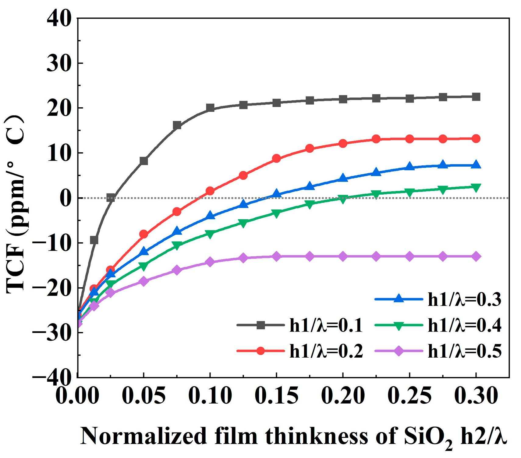
In order to suppress the shift of the operating frequency of the SAW device with temperature changes, this paper investigates the temperature effects on the ZnO piezoelectric film and the SiO2 temperature complementary layer in the Sezawa mode. Lower TCF is also an extremely important performance index for high-frequency SAW devices. ZnO piezoelectric film is known to have a TCF of approximately −28 ppm/°C. The TCF of the device can be significantly improved by adding SiO2 with a positive TCF between the piezoelectric film and the diamond substrate.
Figure 5 shows the TCF in ZnO/SiO2/diamond structures producing the Sezawa mode at different normalized thicknesses of ZnO and SiO2. When h2/λ = 0.1, 0.2, 0.3, and 0.4, it is observed that the Sezawa mode shows positive TCF values with increasing SiO2 thickness; thus, a zero TCF can be obtained. The effect of SiO2 on the TCF of the Sezawa mode decreases gradually for larger values of h2/λ because most of the acoustic energy is confined within the ZnO piezoelectric film. The present simulation results show that the Sezawa wave excited by this structure in the absence of electrode loading not only has obvious advantages over the Rayleigh wave in terms of k2 and vp but also has favorable temperature stability.

3.3. Impact of Electrode Thickness on SAW Propagation Properties

When the piezoelectric film’s surface is covered with a metallic IDT, the mass loading effect of the metallic electrode becomes non-negligible [31]. This section aims to investigate the impact of the IDT electrode on the propagation characteristics of SAW when h1 and h2 are set to 0.4 λ and 0.2 λ, respectively. The vp and k2 of the Rayleigh and Sezawa modes are compared and analyzed for various electrode normalized thicknesses (h3/λ).
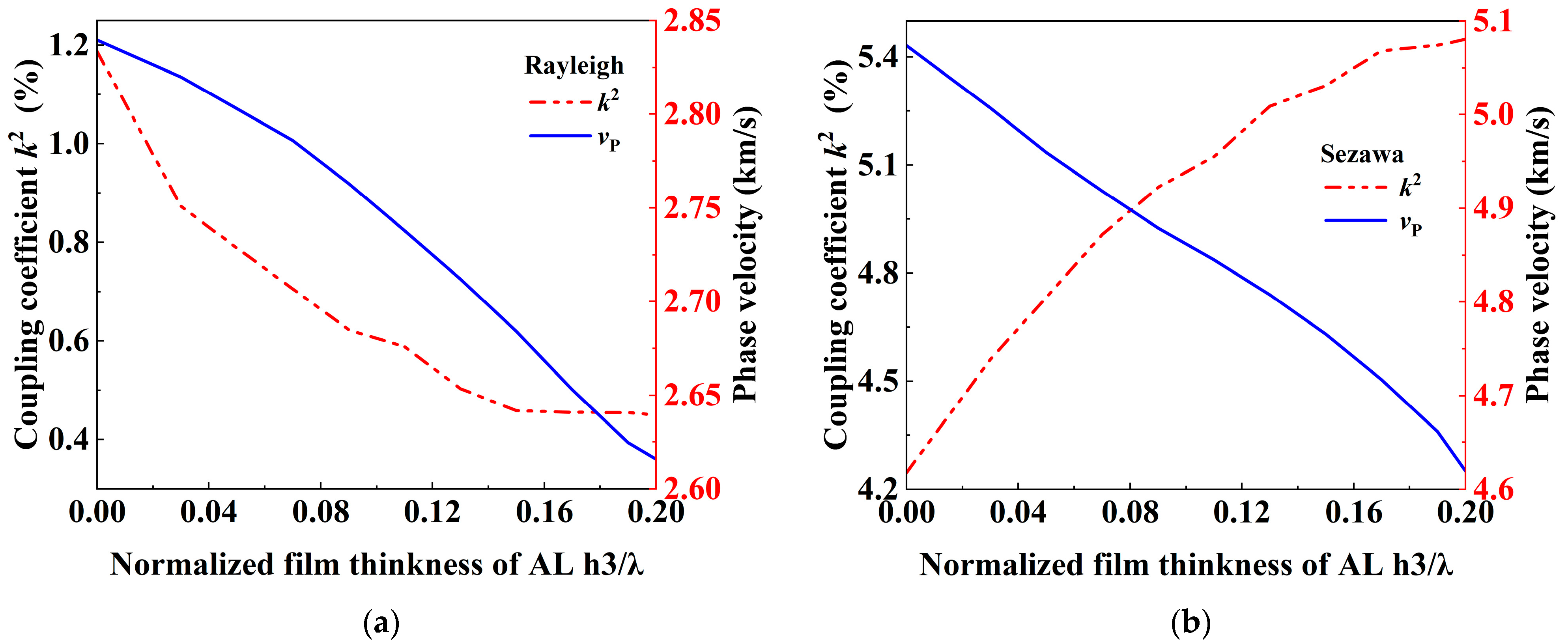
For the Rayleigh and Sezawa modes excited by this structure, as h3/λ increases from 0 to 0.2, Figure 6 illustrates how various electrode thicknesses affect both admittance characteristics. The admittance value of the Sezawa mode first increases and then decreases with the electrode thickness. The cause of this phenomenon is a decrease in electrode resistance and an increase in conductance when h3/λ is increased from 0.04 to 0.08; the reason for the decrease in conductance in the range of h3/λ from 0.16 to 0.20 could be an increase in acoustic impedance. Moreover, the Sezawa mode has significant advantages over the Rayleigh mode. As shown in Figure 7a, the vp of the Rayleigh mode changes from 2838 m/s to 2615 m/s, and as depicted in Figure 7b, the vp of the Sezawa mode changes from 5064 m/s to 4623 m/s. In addition, the k2 of the Rayleigh wave decreases gradually with increasing electrode thickness, from approximately 1.2% to approximately 0.4%. The k2 of the Sezawa wave increases gradually, from approximately 4.2% to approximately 5.4%. In order to obtain a higher k2 value while keeping vp at a higher value, h3 = 0.08 λ is chosen in this paper, i.e., k2 is 4.9% and vp is 4892 m/s.
In summary, in this paper, under consideration of electrode loading, the Sezawa mode still exhibits a larger k2 and vp compared to the Rayleigh mode, which makes it possible to use the Sezawa mode in the fabrication of SAW devices with high frequencies and low TCFs.

3.4. Modal Analysis of Rayleigh and Sezawa Modes

Finding the vibration mode of the acoustic waves on the IDT/ZnO/SiO2/diamond structure designed in this paper is crucial, as there are multiple modes, including Rayleigh, Sezawa, and high-order Sezawa modes, which coexist in the same layered structure. The propagation velocity of acoustic waves in the ZnO piezoelectric film is lower than that of acoustic waves in the diamond substrate.
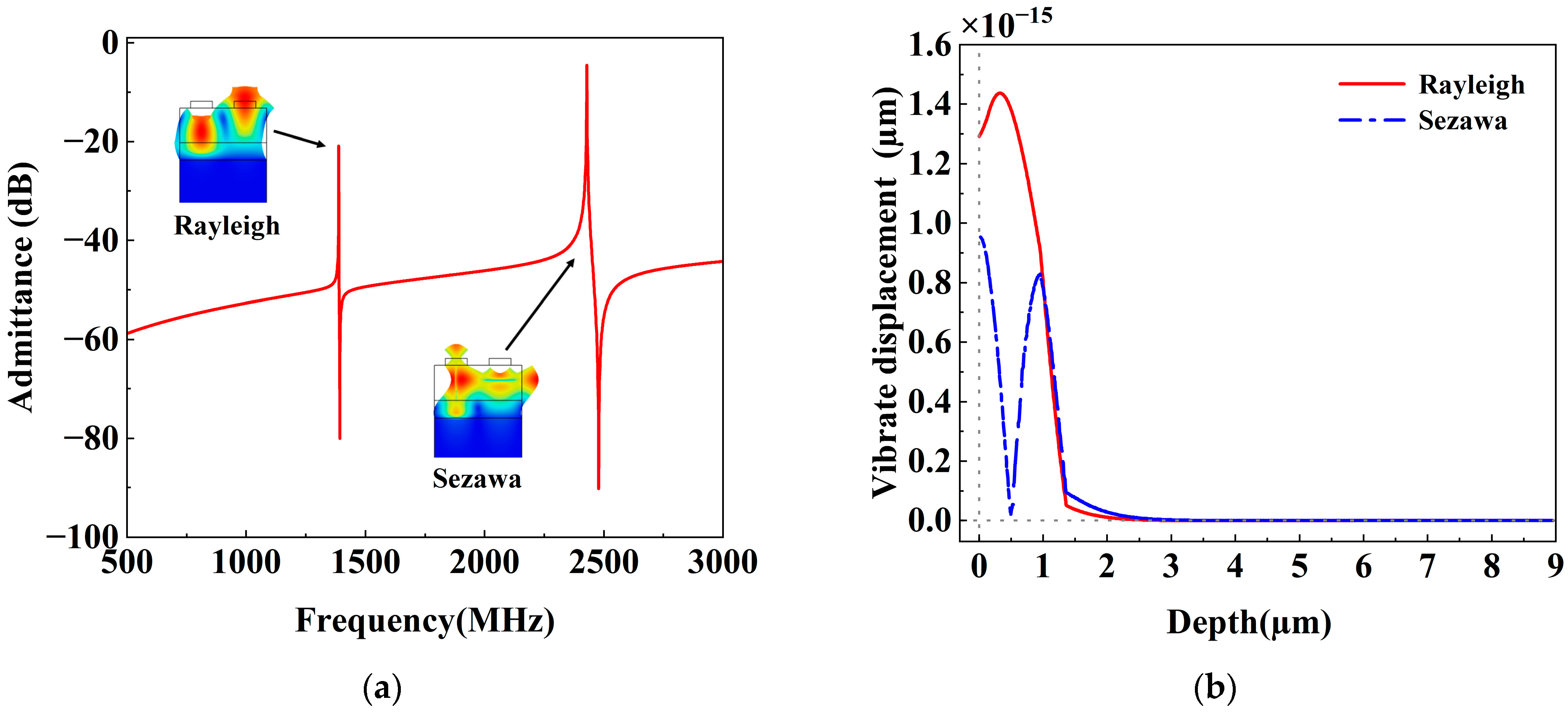
Figure 8 shows the Rayleigh and Sezawa mode displacement field distributions in the z direction versus normalized depth when h1, h2, and h3 are 0.4 λ, 0.2 λ, and 0.08 λ, respectively. Figure 8a shows a typical simulated Y11 response of the SAW resonator with this structure. It can be clearly seen that the device exhibits two different resonance frequencies. The acoustic field of the Rayleigh mode is primarily dispersed on the ZnO surface, whereas the acoustic field of the Sezawa mode is primarily spread throughout the ZnO piezoelectric layer and the SiO2 layer, as seen in Figure 8b. Figure 9 shows the proposed device’s displacement against substrate depth in both Rayleigh and Sezawa modes.

3.5. Resonator Design and Simulation

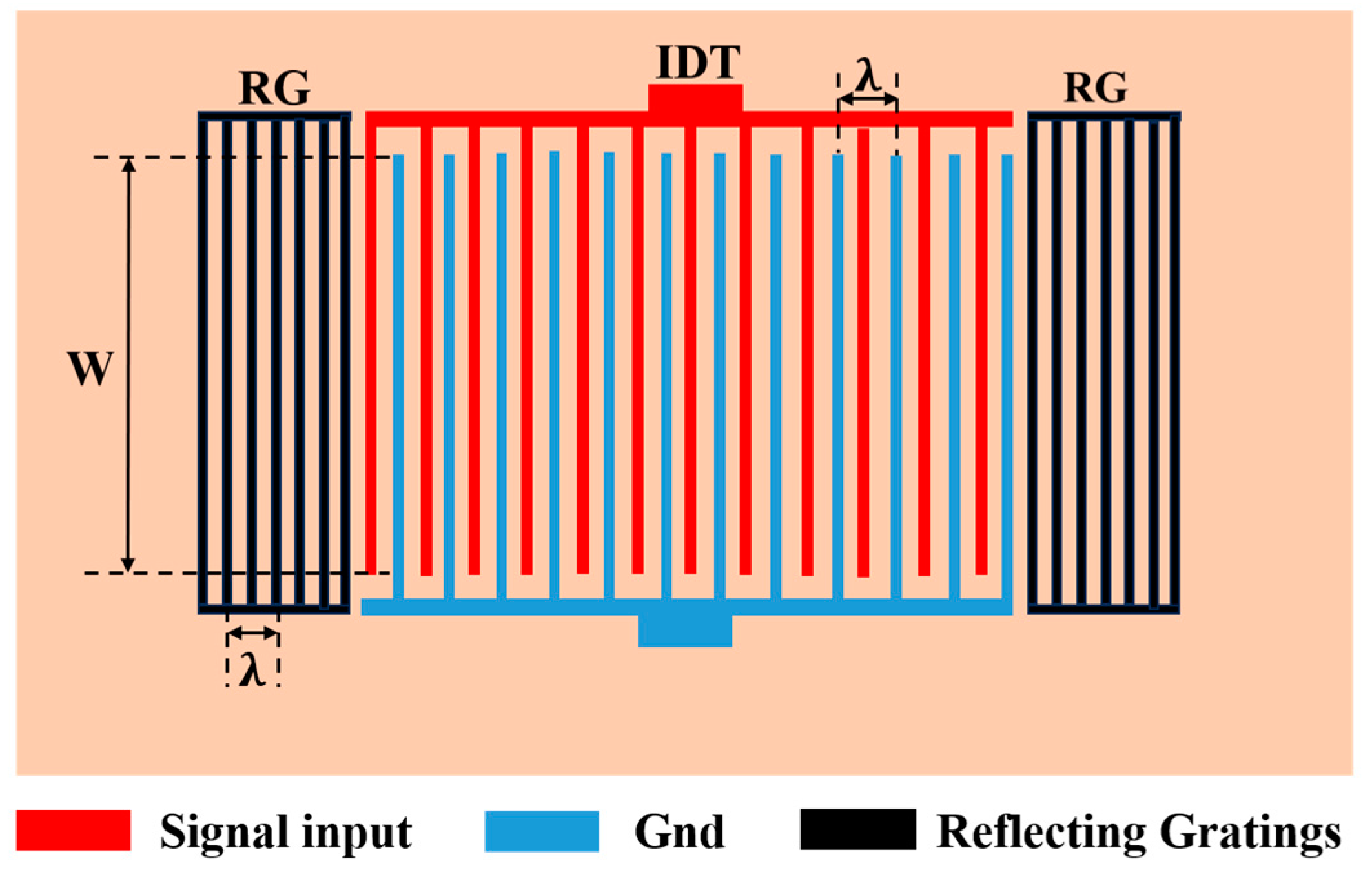
As both SAW-related sensors and filters are fundamentally constructed based on resonators, the analysis of resonator performance impacts becomes crucial. Figure 10 illustrates a schematic diagram of a single-port resonator structure. Single-port resonators typically consist of the IDT and reflecting grating (RG). The IDT refers to metal electrodes arranged in a crossed pattern on a piezoelectric substrate, divided into an input port and a ground port. The portion of the interdigital electrode’s crossed arrangement length is referred to as the acoustic aperture. This section concludes with the design of a SAW resonator with the coexistence of Rayleigh and Sezawa modes using this laminated structure.
The Q, as an important indicator of resonators, is primarily determined by the pairs of the RG, IDT, and the aperture width (W). In this section, we will investigate the influence of the number of the IDT pairs (Nt) and the W on the Q value of the resonator. This study fixes the number of the RG at 25 pairs and then explores the impact of different Nt and W values on the electrical performance of the IDT/ZnO/SiO2/diamond multilayer resonator structure. The thickness of each layer in the resonator is determined based on the results from the previous section.
When studying the impact of Nt, we utilized the array functionality of COMSOL, gradually increasing Nt from 70 pairs to 150 pairs while keeping W fixed at 20 λ to simulate the effects of different Nt values on the resonator. The simulation results are presented in terms of the Y11 parameter. As seen in Figure 11a, with the increase in Nt, the peaks at the resonance and anti-resonance frequencies of the Sezawa wave show a significant rise, indicating an increase in admittance values. This phenomenon is attributed to the better confinement of energy within the resonator as Nt increases. Simultaneously, there is minimal change in the resonance and anti-resonance frequencies, i.e., k2 shows no significant variation. To assess the changes in Q values, this study employs the −3 dB bandwidth method [32]. Figure 11b illustrates the magnitudes and trends of Qs and Qp values obtained for different Nt values. As Nt increases from 70 pairs to 150 pairs, the corresponding Q values at the resonance (Qs) and anti-resonance (Qp) points both show improvement, with Qs changing from 835.2 to 987.1, and Qp changing from 1486.7 to 1627.5. Clearly, the change in Qp is more pronounced.
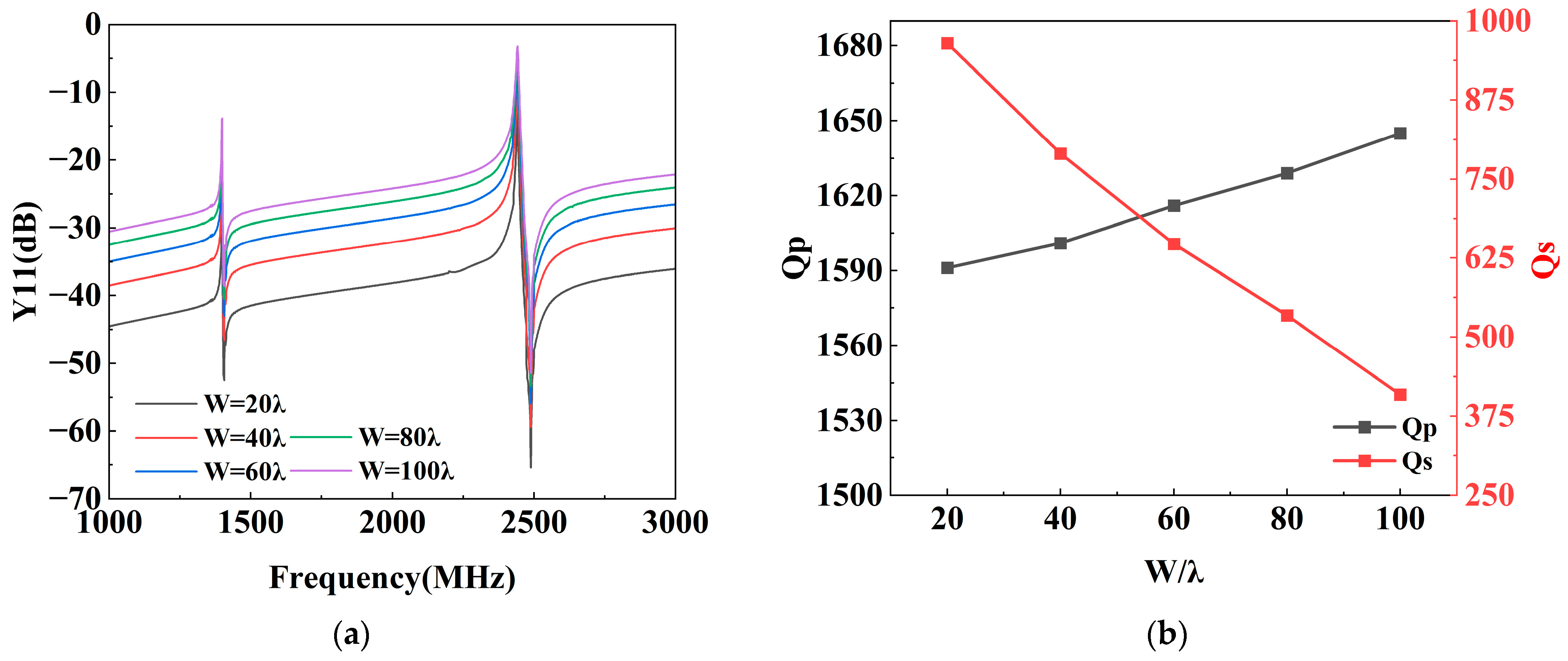
To achieve a higher Qs and Qp while avoiding excessively large device sizes, this study maintains the IDT pairs at a constant value of 130 and proceeds to investigate the impact of W on the resonator. Utilizing the finite element method for parameterized simulations, W is varied in increments of 20 λ, ranging from 20 λ to 100 λ. Figure 12a depicts a schematic of Y11 under different W values, showing an increase in the peaks of Sezawa wave resonance and anti-resonance frequencies, representing an increase in admittance values. Furthermore, k2 remains relatively unchanged. Figure 12b illustrates the magnitudes and trends of Qp and Qs values for different W values. The results indicate a slight increase in Qp, rising from 1591.3 to 1645.8. Conversely, Qs decreases from 964.8 to 408.6, which is attributed to the increased electrode resistance resulting from the larger W.
In summary, choosing appropriate values for Nt and W can enhance the performance of the resonator, but an increase in both parameters leads to a larger device size. Therefore, the selection of Nt and W should be based on the desired performance of the SAW device, the required dimensions, and the complexity of the manufacturing process.
The final structural design parameters of this paper are shown in Table 2.

4. Discussion

This work revealed that the optimization of the proposed structure avoids spurious resonances arising from the coupling of multiple modes since the Rayleigh and Sezawa modes are distant in the frequency domain and do not interfere with each other. For the field of SAW filters, the larger k2 and high vp achieved by this multilayer structure help to construct high-frequency broadband filters, and the zero TCF helps to improve the operating frequency stability of the filters, which is especially promising for applications in the communications field, where the band spacing is much narrower. Future work will proceed to fabricate and characterize SAW devices based on simulations. Comparative analyses of the simulation and experimental results will be carried out to verify the scientific validity of this study.

5. Conclusions

In this paper, a ZnO/SiO2/diamond multilayer structure was proposed, and the effect of each structural parameter on the acoustic properties of the Rayleigh and Sezawa waves excited by this structure was analyzed using the COMSOL finite element method. When the ZnO piezoelectric film is h1 = 0.4 λ, the SiO2 temperature complementary layer is h2 = 0.2 λ and the electrode thickness is h3 = 0.08 λ, while the characteristic frequency of the Sezawa wave is 2446 MHz, k2 is 4.9%, and vp is 4892 m/s. Because the characteristic frequency of the Rayleigh wave is 1388 MHz, k2 is 0.65%, and vp is 2776 m/s, the k2 and vp of the Sezawa wave are improved by 753% and 176% compared those of to the Rayleigh wave. Moreover, k2 and vp are increased by approximately 5 times and 1.5 times, respectively, compared to single-crystal ZnO devices. Eventually, the influence of aperture width and the number of IDTs on the admittance characteristics and the changing patterns of the Q values in a single-port resonator will be investigated. In conclusion, parameters can be judiciously selected based on specific requirements during the device fabrication process. This work provides an alternative approach for achieving high frequencies, favorable temperature stability, and miniaturization in ZnO devices, opening up possibilities for future applications in SAW sensors and filters.

Author Contributions

Conceptualization, G.C. and H.W.; formal analysis, G.C. and H.W.; funding acquisition, H.W.; investigation, P.Z. and H.W.; methodology, G.C. and P.Z.; resources, H.W. and P.Z.; software, G.C. and P.Z.; validation, G.C.; writing—original draft, G.C.; writing—review and editing, G.C. All authors have read and agreed to the published version of the manuscript.

Funding

This research was funded by the Fundamental Research Program Shanxi Province (20210302123034) and the Fund for Shanxi ‘1331 Project’ Key Subject Construction (1331KSC).

Institutional Review Board Statement

Not applicable.

Informed Consent Statement

Not applicable.

Data Availability Statement

The data presented in this study are available in article.

Acknowledgments

The authors are grateful for the support of the open project of the Key Laboratory of Instrumentation Science and Dynamic Measurement, Ministry of Education, North University of China.

Conflicts of Interest

The authors declare no conflicts of interest.

References

  1. Hashimoto, K. RF Bulk Acoustic Wave Filters for Communications; ARTECH House: Norwood, MA, USA, 2009. [Google Scholar]
  2. Ruby, R. A Snapshot in Time: The Future in Filters for Cell Phones. IEEE Microw. Mag. 2015, 16, 46–59. [Google Scholar] [CrossRef]
  3. Park, M.; Hao, Z.; Dargis, R.; Clark, A.; Ansari, A. Epitaxial Aluminum Scandium Nitride Super High Frequency Acoustic Resonators. J. Microelectromech. Syst. 2020, 29, 490–498. [Google Scholar] [CrossRef]
  4. Zou, J.; Yantchev, V.; Iliev, F.; Plessky, V.; Samadian, S.; Hammond, R.B.; Turner, P.J. Ultra-Large-Coupling and Spurious-Free SH 0 Plate Acoustic Wave Resonators Based on Thin LiNbO3. IEEE Trans. Ultrason. Ferroelectr. Freq. Control. 2020, 67, 374–386. [Google Scholar] [CrossRef] [PubMed]
  5. Guo, Y.; Kadota, M.; Tanaka, S. Investigation on the Temperature Coefficient of Frequency Performance of LiNbO3 on Quartz and Glass Surface Acoustic Wave Resonators. Jpn. J. Appl. Phys. 2023, 62, SJ1024. [Google Scholar] [CrossRef]
  6. Zhu, J.; Wang, H.; Zhang, F.; Ding, Q. High-Performance SAW Low Temperature Sensors with Double Electrode Transducers Based on 128° YX LiNbO3. Micromachines 2022, 13, 1912. [Google Scholar] [CrossRef] [PubMed]
  7. Li, Q.; Fu, S.-L.; Song, C.; Wang, G.-Y.; Zeng, F.; Pan, F. Improved Resistance to Electromigration and Acoustomigration of Al Interdigital Transducers by Ni Underlayer. Rare Met. 2018, 37, 823–830. [Google Scholar] [CrossRef]
  8. Qian, J.; Li, C.; Qian, L.; Li, M.; Li, H.; Yang, B. Three-Dimensional Finite Element Simulation of Love Mode Surface Acoustic Wave in Layered Structures Including ZnO Piezoelectric Film and Diamond Substrate. Diam. Relat. Mater. 2018, 88, 123–128. [Google Scholar] [CrossRef]
  9. Assouar, M.B.; Elmazria, O.; Jiménez Riobóo, R.; Sarry, F.; Alnot, P. Modelling of SAW Filter Based on ZnO/Diamond/Si Layered Structure Including Velocity Dispersion. Appl. Surf. Sci. 2000, 164, 200–204. [Google Scholar] [CrossRef]
  10. Su, R.; Shen, J.; Lu, Z.; Xu, H.; Niu, Q.; Xu, Z.; Zeng, F.; Song, C.; Wang, W.; Fu, S.; et al. Wideband and Low-Loss Surface Acoustic Wave Filter Based on 15° YX-LiNbO₃/SiO₂/Si Structure. IEEE Electron Device Lett. 2021, 42, 438–441. [Google Scholar] [CrossRef]
  11. Ishihara, M.; Nakamura, T.; Kokai, F.; Koga, Y. Preparation of AlN and LiNbO3 Thin Films on Diamond Substrates by Sputtering Method. Diam. Relat. Mater. 2002, 11, 408–412. [Google Scholar] [CrossRef]
  12. Lamanna, L.; Rizzi, F.; Guido, F.; Algieri, L.; Marras, S.; Mastronardi, V.M.; Qualtieri, A.; De Vittorio, M. Flexible and Transparent Aluminum-Nitride-Based Surface-Acoustic-Wave Device on Polymeric Polyethylene Naphthalate. Adv. Electron. Mater. 2019, 5, 1900095. [Google Scholar] [CrossRef]
  13. Fu, S.; Wang, W.; Qian, L.; Li, Q.; Lu, Z.; Shen, J.; Song, C.; Zeng, F.; Pan, F. High-Frequency Surface Acoustic Wave Devices Based on ZnO/SiC Layered Structure. IEEE Electron Device Lett. 2019, 40, 103–106. [Google Scholar] [CrossRef]
  14. Li, Q.; Qian, L.; Fu, S.; Song, C.; Zeng, F.; Pan, F. Characteristics of One-Port Surface Acoustic Wave Resonator Fabricated on ZnO/6H-SiC Layered Structure. J. Phys. D Appl. Phys. 2018, 51, 145305. [Google Scholar] [CrossRef]
  15. Luo, J.; Quan, A.; Fu, C.; Li, H. Shear-Horizontal Surface Acoustic Wave Characteristics of a (110) ZnO/SiO2/Si Multilayer Structure. J. Alloys Compd. 2017, 693, 558–564. [Google Scholar] [CrossRef]
  16. Fu, S.; Li, Q.; Gao, S.; Wang, G.; Zeng, F.; Pan, F. Quality-Enhanced AlN Epitaxial Films Grown on c-Sapphire Using ZnO Buffer Layer for SAW Applications. Appl. Surf. Sci. 2017, 402, 392–399. [Google Scholar] [CrossRef]
  17. Zhang, H.; Wang, H. Investigation of Surface Acoustic Wave Propagation Characteristics in New Multilayer Structure: SiO2/IDT/LiNbO3/Diamond/Si. Micromachines 2021, 12, 1286. [Google Scholar] [CrossRef] [PubMed]
  18. Maouhoub, S.; Aoura, Y.; Mir, A. FEM Simulation of Rayleigh Waves for SAW Devices Based on ZnO/AlN/Si. Microelectron. Eng. 2015, 136, 22–25. [Google Scholar] [CrossRef]
  19. Su, R.; Fu, S.; Shen, J.; Chen, Z.; Lu, Z.; Yang, M.; Wang, R.; Zeng, F.; Wang, W.; Song, C.; et al. Enhanced Performance of ZnO/SiO2/Al2O3 Surface Acoustic Wave Devices with Embedded Electrodes. ACS Appl. Mater. Amp. Interfaces 2020, 12, 42378–42385. [Google Scholar] [CrossRef]
  20. Wang, Y.; Zhang, S.-Y.; Fan, L.; Shui, X.-J.; Zhang, Z.-N.; Wasa, K. Characteristics of Surface Acoustic Waves Excited by (1120) Zno Films Deposited on R-Sapphire Substrates. IEEE Trans. Ultrason. Ferroelectr. Freq. Control. 2013, 60, 1213–1218. [Google Scholar] [CrossRef]
  21. Fang, J.; Wu, Z. Generalized Perfectly Matched Layer-an Extension of Berenger’s Perfectly Matched Layer Boundary Condition. IEEE Microw. Guid. Wave Lett. 1995, 5, 451–453. [Google Scholar] [CrossRef]
  22. Kannan, T. Finite Element Analysis of Surface Acoustic Wave Resonators. Master’s Thesis, University of Saskatchewan, Saskatoon, Canada, 2006. [Google Scholar]
  23. Tomar, M.; Gupta, V.; Sreenivas, K.; Mansingh, A. Temperature Stability of ZnO Thin Film SAW Device on Fused Quartz. IEEE Trans. Device Mater. Reliab. 2005, 5, 494–500. [Google Scholar] [CrossRef]
  24. Maouhoub, S.; Aoura, Y.; Mir, A. FEM Simulation of AlN Thin Layers on Diamond Substrates for High Frequency SAW Devices. Diam. Relat. Mater. 2016, 62, 7–13. [Google Scholar] [CrossRef]
  25. Aslam, M.; Jeoti, V.; Karuppanan, S.; Malik, A.; Iqbal, A. FEM Analysis of Sezawa Mode SAW Sensor for VOC Based on CMOS Compatible AlN/SiO₂/Si Multilayer Structure. Sensors 2018, 18, 1687. [Google Scholar] [CrossRef] [PubMed]
  26. Benetti, M.; Cannata, D.; Di Pictrantonio, F.; Verona, E. Growth of AlN Piezoelectric Film on Diamond for High-Frequency Surface Acoustic Wave Devices. IEEE Trans. Ultrason. Ferroelectr. Freq. Control. 2005, 52, 1806–1811. [Google Scholar] [CrossRef] [PubMed]
  27. Li, Y.; Shao, M.; Jiang, B.; Cao, L. Surface Acoustic Wave Pressure Sensor and Its Matched Antenna Design. Meas. Control. 2019, 52, 947–954. [Google Scholar] [CrossRef]
  28. Qianliang, X. Simulation of Surface Acoustic Wave Tag Based on COMSOL. Yadian Shengguang 2012, 34, 494–497. [Google Scholar]
  29. Kaletta, U.C.; Santos, P.V.; Wolansky, D.; Scheit, A.; Fraschke, M.; Wipf, C.; Zaumseil, P.; Wenger, C. Monolithic Integrated SAW Filter Based on AlN for High-Frequency Applications. Semicond. Sci. Technol. 2013, 28, 065013. [Google Scholar] [CrossRef]
  30. Zhou, C.; Yang, Y.; Cai, H.; Ren, T.-L.; Chan, M.; Yang, C.Y. Temperature-Compensated High-Frequency Surface Acoustic Wave Device. IEEE Electron Device Lett. 2013, 34, 1572–1574. [Google Scholar] [CrossRef]
  31. Li, L.; Wang, F.; Li, K.; Han, Y.; Hu, K.; Sun, Z.; Xie, Y.; Kong, D.; Song, D.; Qian, L.; et al. Effect of Interdigital Transducers Structure on Insertion Loss of High-Frequency Surface Acoustic Wave Devices. J. Mater. Sci. Mater. Electron. 2022, 33, 22017–22026. [Google Scholar] [CrossRef]
  32. Feld, D.A.; Parker, R.; Ruby, R.; Bradley, P.; Dong, S. After 60 Years: A New Formula for Computing Quality Factor Is Warranted. In Proceedings of the 2008 IEEE Ultrasonics Symposium, Beijing, China, 2–5 November 2008. [Google Scholar]
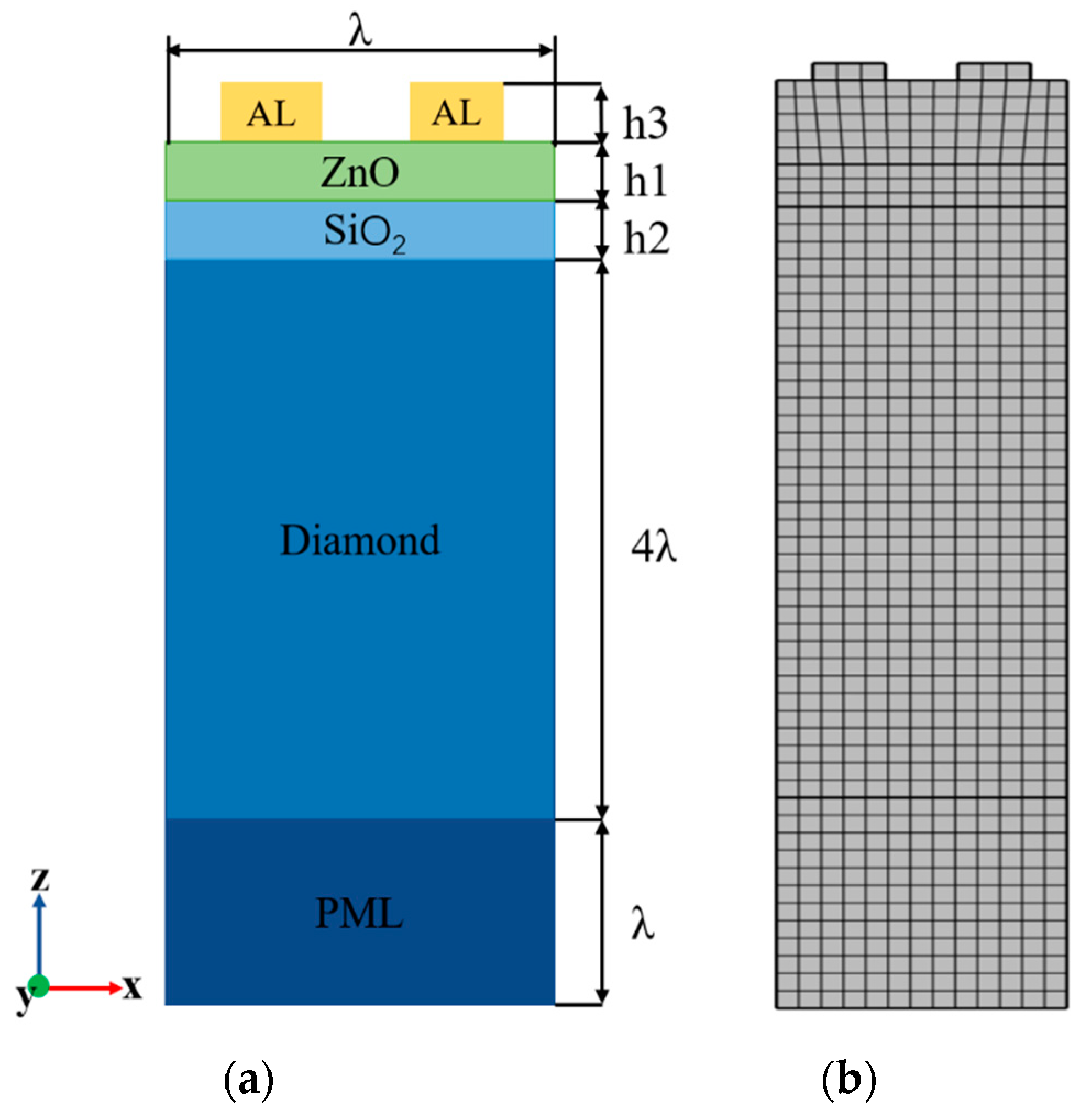
Figure 1. Schematic diagram of the construction model: (a) IDT/ZnO/SiO2/diamond; (b) mesh delineation.
Applsci 14 00874 g001
Figure 2. Resonant modes of Rayleigh and Sezawa waves: (a) Rayleigh wave; (b) Sezawa wave.
Applsci 14 00874 g002
Figure 3. Rayleigh and Sezawa waves k2 as functions of h2/λ with different h1/λ values: (a) Rayleigh wave; (b) Sezawa wave.
Applsci 14 00874 g003
Figure 4. Rayleigh and Sezawa wave velocities as functions of h2/λ with different h1/λ values: (a) Rayleigh wave; (b) Sezawa wave.
Applsci 14 00874 g004
Figure 5. TCF of Sezawa wave variation with SiO2 normalized thickness (h2/λ).
Applsci 14 00874 g005
Figure 6. Rayleigh and Sezawa modes’ admittance dependence on electrode normalized thickness (h3/λ).
Applsci 14 00874 g006
Figure 7. Rayleigh and Sezawa modes’ k2 and vp dependence on electrode normalized thickness (h3/λ): (a) Rayleigh wave; (b) Sezawa wave.
Applsci 14 00874 g007
Figure 8. (a) The admittance of the IDT/ZnO/SiO2/diamond structure, and the corresponding resonant mode, where h3/λ = 0.08, h2 = 0.2 λ, and h1/λ = 0.4. (b) z-direction displacement field distributions of Rayleigh and Sezawa waves as a function of depth.
Applsci 14 00874 g008
Figure 9. Designed device’s displacement against substrate depth in both Rayleigh and Sezawa modes: (a) Rayleigh wave; (b) Sezawa wave.
Applsci 14 00874 g009
Figure 10. Schematic structure of single-port SAW resonator.
Applsci 14 00874 g010
Figure 11. Effect of Nt on Y11 performance and Q value: (a) Effect of Nt on Y11 performance; (b) the values of Qs and Qp vary with Nt.
Applsci 14 00874 g011
Figure 12. Effect of W on Y11 performance and Q value: (a) effect of W on Y11 performance; (b) the values of Qs and Qp vary with W/λ.
Applsci 14 00874 g012
Table 1. Material parameters used in calculations.
ItemSymbolAlZnOSiO2Diamond
Elastic constant (1011 N/m2)C111.112.0960.78511.531
C120.591.2050.1610.864
C130.591.0460.1610.864
C331.112.1060.78511.531
C440.260.4230.3115.333
Temperature coefficients of elastic constants (10−4/°C)TC11−5.9−1.122.39−0.14
TC13−0.8−1.615.84−0.57
TC33−5.9−1.232.39−0.14
TC44−5.2−0.701.51−0.125
Piezoelectric constants (C/m2)e15-−0.48--
e31-−0.573--
e33-1.321--
Relative dielectric constantsε11/ ε018.553.325.67
ε33/ε0110.23.325.67
Mass density (103 kg/m3)p2.75.6652.23.512
Temperature coefficients of mass density (10−6/°C)TP−1.65−10.1−54−3.6
Table 2. Design parameters used in this paper.
ItemSymbolValue
Wavelength (um)λ2
ZnO thickness (um)h10.4 λ
SiO2 thickness (um)h20.2 λ
Al electrode thicknessh30.08 λ
Metallization rateMR50%
IDT pairsNt130
Aperture width (um)W40 λ
Reflecting grating pairsNg25
Disclaimer/Publisher’s Note: The statements, opinions and data contained in all publications are solely those of the individual author(s) and contributor(s) and not of MDPI and/or the editor(s). MDPI and/or the editor(s) disclaim responsibility for any injury to people or property resulting from any ideas, methods, instructions or products referred to in the content.