Optimization of Additive and Current Conditions for Void-Free Filled Through-Silicon Via


School of Advanced Materials Science and Engineering, Sungkyunkwan University, Suwon, Gyeonggi-do 440-746, Korea
*
Author to whom correspondence should be addressed.
Appl. Sci. 2018, 8(11), 2135; https://doi.org/10.3390/app8112135
Submission received: 30 September 2018
/
Revised: 24 October 2018
/
Accepted: 29 October 2018
/
Published: 2 November 2018
(This article belongs to the Special Issue Selected Papers from IUMRS-ICEM 2018)
Abstract
:Featured Application
This paper presents a method for optimizing void-free copper filling of through-silicon vias (TSVs) through the interaction of additives and current density for applications in 3D integrated circuits such as those used in dynamic random access memory (DRAM) and complementary metal-oxide semiconductor (CMOS) image sensors.
Abstract
Studies of through-silicon vias (TSVs) have become important owing to the increasing demand for 3D packaging. To obtain high-performance devices, it is important to fill the holes inside TSVs without voids. In this study, poly(ethylene glycol), bis-(3-sodiumsulfopropyl disulfide), and Janus Green B are used as a suppressor, accelerator, and leveler, respectively, to achieve void-free filling of a TSV. The optimum conditions for the additives were studied, and electrochemical analysis was performed to confirm their effects. Different current conditions, such as pulse, pulse-reverse, and periodic pulse-reverse, were also employed to enhance the filling properties of copper (Cu) for a TSV with a hole diameter of 60 µm and depth/hole aspect ratios of 2, 2.5, and 3. The behavior of Cu filling was observed through a cross-sectional analysis of the TSV after Cu plating under various conditions.
1. Introduction
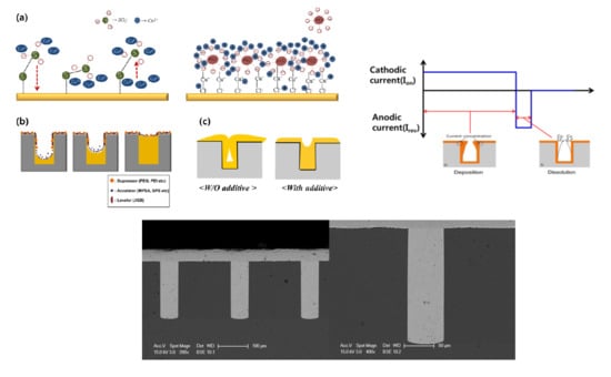
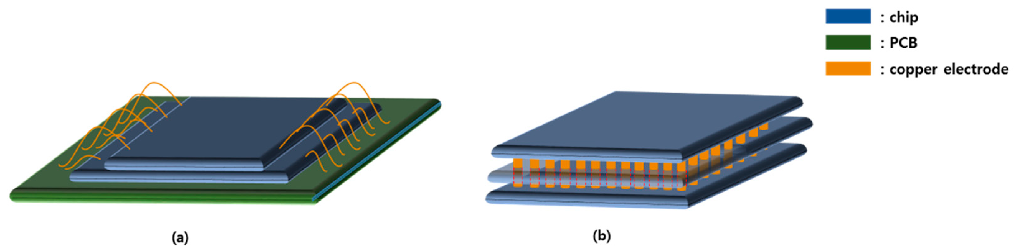
To meet the lightweight, high-speed signal transport, and low-power consumption trends of the electronic packaging industry, devices require miniaturization and high-density packaging through compact packaging technology [1,2]. Therefore, chip fabrication and interconnection form an advanced spectrum in the microelectronics industry, where specifications for high performance and miniaturization of semiconductors continue to change every 18 months [3]. A candidate to meet such compact chip packaging technology demands is 3D chip stacking, because of its advantage of volume reduction compared to conventional package-on-package technology [1,2,4]. As demonstrated in Figure 1, there are two types of 3D lamination processes. Figure 1 is a schematic diagram of wire bonding. The stacked chips on the printed circuit board (PCB) are connected by wire as shown in fig1a.; 3D lamination through wire bonding can be used to improve the performance of the device. However, there is a limit to miniaturization as space is required to prevent signal noise and interference between the chip and the wire [5]. To overcome these disadvantages, technical developments to commercialize 3D integrated circuits using through-silicon vias (TSVs) have been actively studied in recent years [6]. A TSV is a high-performance vertical electrical connection technique used as an alternative to wire bonding and fillip chips to create 3D integrated circuits. As presented in Figure 1b, TSVs directly connect between stacked chips. Compared to other methods such as wire bonding technology, the interconnect and device density are higher while the length of the connections is shorter [7]. To achieve the characteristics of TSVs, it is important to completely fill the TSV hole without voids [2,5,8,9].
In this study, the results before and after pretreatment were compared, and the optimal conditions for void-free filling were determined by varying the concentrations of additives poly(ethylene glycol) (PEG), bis-(3-sodiumsulfopropyl disulfide) (SPS), Janus Green B (JGB), as well as current parameters.
2. Materials and Methods
TSV samples with blind vias AR 1:2–1:3 (about 60 µm in diameter, about 120 µm/150 µm/180 µm in depth) on Si substrate were prepared using the Bosch process of inductively coupled plasma reactive ion etching (ICP-RIE) for the TSV filling experiment [10,11]. Si wafer of 1 × 1 cm2 size was used for small scale deposition. A nickel phosphorus (NiP) layer was formed as the diffusion barrier and seed layer through electroless plating. After forming the NiP layer, pretreatment was conducted using a vacuum desiccator to remove bubbles in the hole of the TSV after putting the TSV substrate in deionized water (DI). After pretreatment, copper plating was performed.
Table 1 shows the composition of the Cu plating bath. The virgin makeup solution (VMS) for copper plating consists of 0.79 M of CuSO4·5H2O, 1.02 M of H2SO4, and 1.4 mM of Cl−. The additives PEG, SPS, and JGB were used as a suppressor, an accelerator, and a leveler, respectively.
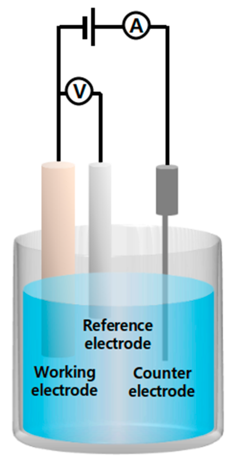
The current conditions were conducted on DC 1 Ampere per Square Deci-metre (ASD) to obtain the additive conditions, and on-reverse conditions were used for void-free filling. Electrochemical analysis was performed on the influence of additives in three electrode cells using the EC-Lab electrochemistry software. Figure 2 shows a schematic diagram of the cyclic voltammetry (CV) analysis setup.
For the CV analysis, a platinum (Pt) disk electrode with a diameter of 1.6 mm was used as the working electrode, and a Pt wire and Ag/AgCl electrode were used as the counter electrode and reference electrode, respectively. The cross-section of the TSV was observed using an optical microscope (OM) and a scanning electron microscope (SEM) in order to investigate the plating tendency inside the TSV according to various plating conditions.
3. Results and Discussion
3.1. Effect of Pretreatment
The effect of pretreatment before plating was confirmed. If the TSV is put into the plating solution without pretreatment, the plating solution may not act on the inside of the hole caused by the air bubbles in the hole. At this time, if the TSV substrate is put in DI water and then into a vacuum desiccator and to create a vacuum state, the bubbles emerge from the hole.
Figure 3 presents the cross-sectional image from an OM before and after pretreatment. The pretreatment results confirm that the filling ratio of the plating was increased by removing the bubbles inside the hole.
3.2. Cyclic Voltammetry (CV) Analysis
The effects of additives during copper plating were confirmed by CV measurement.
CV measurement is an electrochemical technique that measures the current developing in an electrochemical cell under conditions where the voltage is higher than that predicted by the Nernst equation [12]. CV is performed by changing the potential of a working electrode (Ewe) versus Ag/AgCl electrode through a cycle and measuring the resulting current. In the reduction section of the CV curve, the cathode peak potential value represents the voltage value needed for plating. If the cathode peak potential is shifted to a positive value by the additive, then the plating rate can be expected to increase. Conversely, if the cathode peak potential is shifted to a negative value, then the plating rate can be expected to decrease.
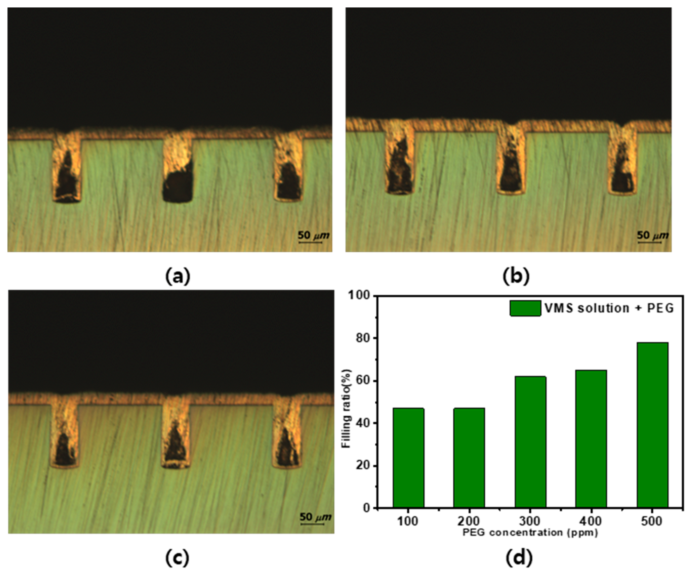
CV measurements were performed between −0.6 V and 0.8 V at a scan rate of 20 mV/s. Figure 4a shows the CV curves corresponding to the behavior of Cu ions in a VMS bath after the addition of PEG. The onset potential for Cu deposition started at −0.03 V without PEG, and the cathode peak potential is observed at −0.192 V. As the amount of PEG increased, the cathode peak potential tended to be negative and shifted toward the negative direction (from −0.18 V to −0.4 V). This means that an amount of shifted energy should be applied to allow the same current to flow, indicating that the reduction reaction shifted to a state where it is difficult to occur. In other words, as PEG concentration increases, plating is suppressed [13,14,15,16,17].
When PEG concentration exceeded 500 ppm, no further negative shift was observed, indicating that the maximum concentration of PEG in the VMS bath is 500 ppm.
Figure 4b shows the CV polarization curves for different SPS concentrations. When SPS was added to PEG with a concentration of 500 ppm, the cathode peak potential and onset potential shifted toward the positive direction. As SPS concentration increased from 1 ppm to 5 ppm, the cathode peak tended to present a positive shift (from −0.35 V to −0.30 V). This means that the reduction potential is reduced, indicating that the plating process speeds up as SPS concentration increases [14,15,16,17,18,19].
However, when SPS concentration exceeded 5 ppm, the peak shifted toward the negative direction. From this point of view, the suitable SPS concentration is expected to be 5 ppm.
As observed in Figure 4c, similar to PEG, when JGB was added to the plating bath, both the cathode peak potential and initiation potential also shifted toward the negative direction [13,16,20]. It can be seen that, as JGB concentration increased from 10 ppm to 50 ppm, the cathode peak potential shifted from −0.35 V to −0.37 V. The peak potential values at JGB concentrations of 30 ppm and 50 ppm were not significantly different and were expected to be saturated at 30 ppm. The CV analysis further demonstrated that the suppressor and leveler suppressed the plating rate, while the accelerator accelerated the plating rate. Based on the CV analysis data, electrodeposition experiments were performed on the different additives.
3.3. Tendency of Plating by Additive
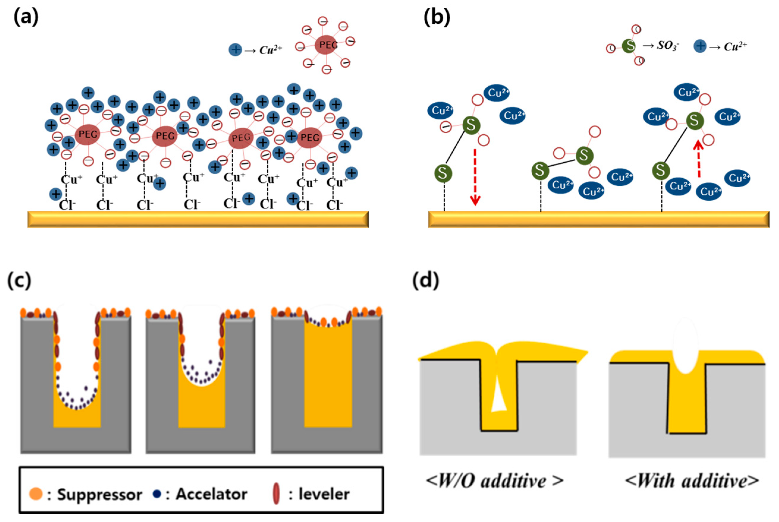
The effects of each additive on plating are presented in Figure 5 [2,4,13,21]. As shown in Figure 5a, PEG and JGB captured Cu+ ions. This cation is strongly adsorbed onto the surface of the wafer owing to electrostatic interaction with the chloride ion (Cl−) on the surface of the Cu electrode, which prevents the precipitation of Cu. As shown in Figure 5b, SPS is an accelerator that promotes the precipitation of Cu through the reaction of the Cu+ ion with the sulfur trioxide ion (SO3−) of SPS. PEG suppressed the plating rate on the surface, SPS accelerated the plating rate in the hole, and JGB suppressed the plating rate at the edge, thereby controlling the clogging of the hole due to the edge effect [2,21].
Copper electroplating was performed with DC 1 ASD (−10 mA/cm2) to confirm the effect of additives on plating. The effect of additive on plating was confirmed by analyzing images taken with an OM.
Figure 6a–d shows the plating cross-sectional image and filling ratio graph according to PEG concentration. The experiment results show that as PEG concentration increased, the filling ratio increased, and the highest filling ratio was observed at 500 ppm. Compared with the CV analysis, it was confirmed that plating occurred inside the TSV as the plating rate of the surface was suppressed and clogging of the hole entrance was controlled by PEG. However, bottom-up filling should be undertaken for void-free filling, but it is difficult to satisfy the condition using only PEG. Therefore, the interaction of 500 ppm of PEG with other additives and current conditions was studied.
Figure 7a–d shows the cross-sectional image of the sample and filling ratio graph according to SPS concentration. A concentration of PEG of 500 ppm as well as the addition of SPS was studied for AR 1:2.5 TSV, with (a), (b), and (c) representing SPS concentrations of 1 ppm, 3 ppm, and 5 ppm, respectively. The addition of 500 ppm PEG and SPS to the VMS bath increased the filling ratio when SPS concentration increased. Also, compared with the PEG test, it is observed that the bottom side is plated even though the aspect ratio is increased. However, when the SPS concentrations of 3 ppm and 5 ppm were compared, plating from the bottom of the hole was observed for 3 ppm but not for 5 ppm. Therefore, the optimum SPS concentration for void-free filling was confirmed in the on-reverse condition.
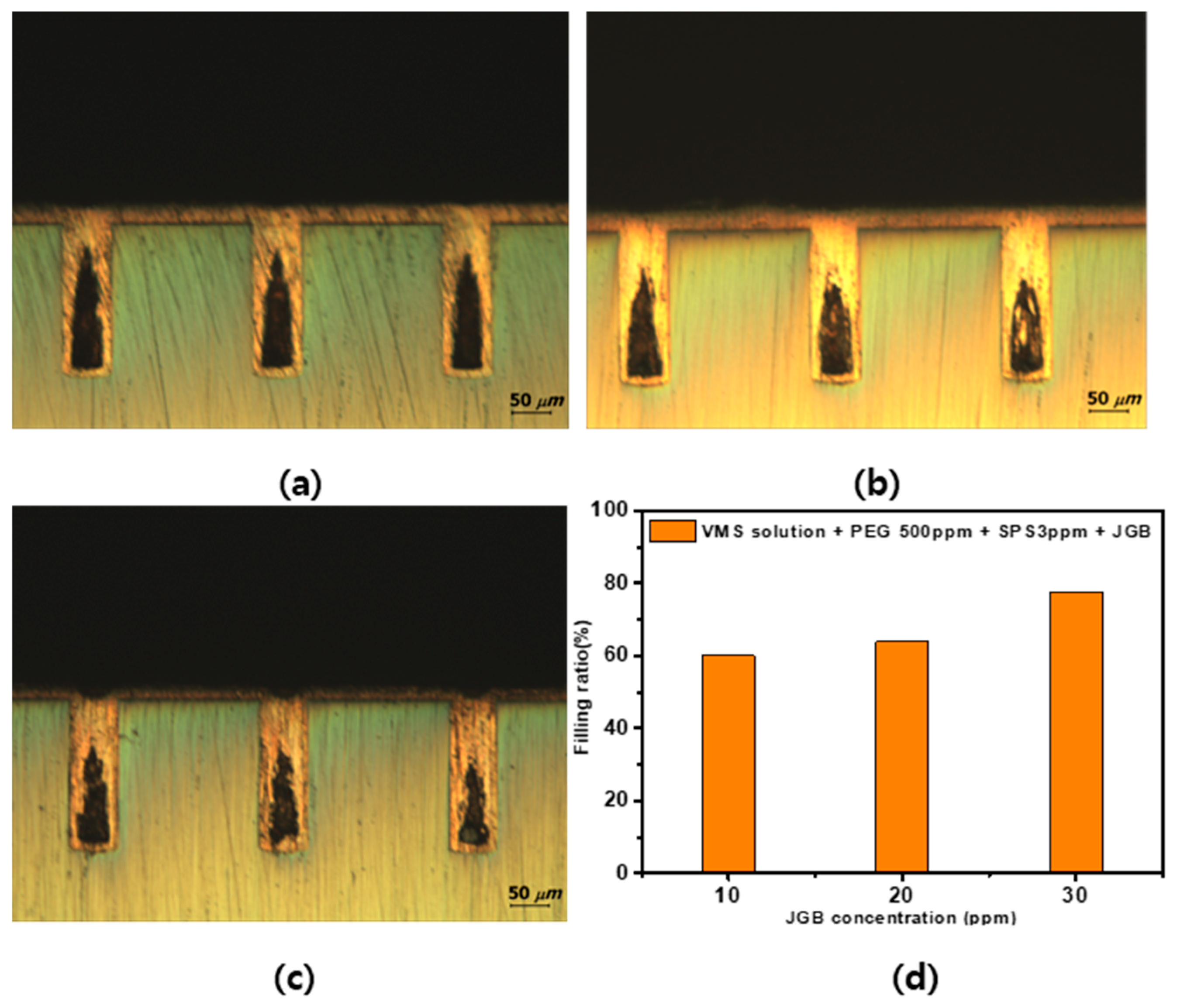
Figure 8a–d demonstrates that the filling ratio increases when JGB concentration increases, and the highest filling ratio was obtained at JGB concentration of 30 ppm. As the amount of additive increased, the rate of clogging of the hole slowed and the proportion of the void was small, but complete filling did not occur. Therefore, complete filling of TSV was performed by pulse plating.
3.4. Effect of On-Reverse Current Condition
Based on the CV curve analysis and DC plating data, the current condition was confirmed when 500 ppm PEG, 3 ppm and 5 ppm SPS, and 30 ppm JGB were added to the basic plating bath.
Figure 9 presents the effect of the on-reverse current on TSV plating [1,21]. Deposition occurred with the on-current while reduction occurred with the reverse current. The effects of reverse current change on plating were investigated, and the additive conditions and current conditions for void-free filling were optimized [21,22].
Firstly, copper electroplating was performed by changing the current conditions for PEG, SPS, and JGB concentrations of 500 ppm, 3 ppm/5 ppm, and 30 ppm, respectively. Table 2 shows the condition of pulse current. On-reverse plating was performed under reverse current conditions of 8 mA/cm2, 16 mA/cm2, and 24 mA/cm2.
At SPS concentration of 3 ppm (Figure 10a–d), the highest TSV filling ratio of approximately 90.57% was obtained with a reverse current of 16 mA/cm2. The presence of voids was attributed to insufficient plating speed in the holes.
Figure 10e–h presents the results of plating with 500 ppm PEG, 5 ppm SPS, and 30 ppm JGB under varying current conditions.
The filling ratio of the TSV was confirmed to be 90% at 8 mA/cm2 and 85% at 24 mA/cm2, and void-free filling occurred at 16 mA/cm2. These results demonstrate that the 5 ppm of SPS accelerates the plating rate in the hole and is sufficient to achieve plating from the bottom. At 8 mA/cm2, it can be seen that the plating thickness of the surface is thick and the inside of the hole is empty. This suggests that the hole was rapidly blocked as the reverse current of 8 mA/cm2 was insufficient for edge reduction to occur. At 24 mA/cm2, the reverse current was too high, and it is deduced that reduction occurred at the bottom. As a result of this experiment, it was confirmed that the ideal conditions for complete filling are additive concentrations of 500 ppm PEG, 5 ppm SPS, 30 ppm JGB for on-current of 10 mA/cm2 and reverse current of 16 mA/cm2.
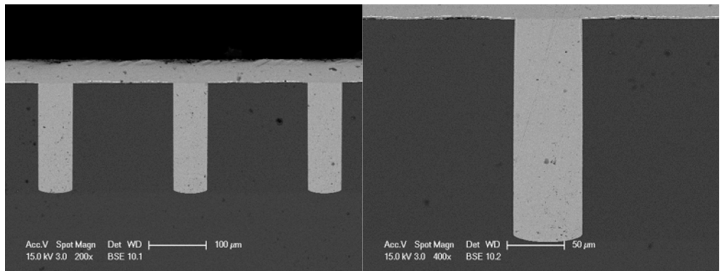
The image of the void-free filled TSV was more clearly confirmed by SEM. Figure 11 represents an SEM image of the void-free filled TSV section.
The experimental results show that the additive and current conditions for void-free filling of a TSV were optimized.
4. Conclusions
In this study, the effects of additives (PEG, SPS, and JGB) on copper electroplating were confirmed using CV analysis. As the concentration of PEG and JGB increased, the suppressing effect on copper plating also increased. As SPS concentration increased, the accelerating effect on copper plating also increased.
Based on the results of the CV analysis, copper electroplating was performed by varying the current and additive conditions, and the filling ratio was observed through cross-sectional analysis. The highest filling ratio was obtained at concentrations of 500 ppm PEG, 5 ppm SPS, and 30 ppm JGB. Thereafter, pulse electroplating was performed with fixed on-current of 10 mA/cm2 and varying reverse current.
When the reverse current was set to 16 mA/cm2, a void-free filled TSV was obtained under optimized plating conditions.
Author Contributions
S.-H.S. designed the experiments, performed the experiments, analyzed the result of the research, and wrote the manuscript; T.-Y.K. and J.-H.P. designed the experiments, and analyzed the result of the research; S.-J.S. reviewed the manuscript, and administered project. All authors approved the final version of the manuscript.
Funding
This work was partly supported by the GRRC program of Gyeonggi province [GRRC Sungkyunkwan] grant number [2017-B01].
Conflicts of Interest
The authors declare no conflict of interest.
References
- Hong, S.C.; Lee, W.G.; Kim, W.J.; Kim, J.H.; Jung, J.P. Reduction of defects in TSV filled with Cu by high-speed 3-step PPR for 3D Si chip stacking. Microelectron. Reliab. 2011, 51, 2228–2235. [Google Scholar] [CrossRef]
- Lu, Y.; Cao, H.Y.; Sun, Q.; Ling, H.Q.; Li, M.; Sun, J.Y. Investigation of competitive adsorption between accelerator and suppressor in TSV copper electroplating. Presented at the 13th International Conference on Electronic Packaging Technology & High Density Packaging, Guilin, China, 13–16 August 2012. [Google Scholar]
- Datta, M. Electrochemical processing technologies in chip fabrication: Challenges and opportunities. Electrochim. Acta 2003, 48, 2975–2985. [Google Scholar] [CrossRef]
- Li, Q.; Ling, H.Q.; Cao, H.Y.; Bian, Z.Y.; Li, M.; Mao, D. Through silicon via filling by copper electroplating in acidic cupric methanesulfonate bBath. Presented at the 2009 International Conference on Electronic Packaging Technology & High Density Packaging, Beijing, China, 10–13 August 2009. [Google Scholar]
- Zhang, Y.; Ding, G.; Wang, H.; Cheng, P.; Liu, R. Optimization of innovative approaches to the shortening of filling times in 3D integrated through-silicon vias (TSVs). J. Micromech. Microeng. 2015, 25, 045009. [Google Scholar] [CrossRef]
- Ngansso, S.; Fischer, P. TSV Through silicon via technology for 3D-integration. Presented at the 2010 IEEE International Memory Workshop, Seoul, Korea, 16–19 May 2010. [Google Scholar]
- Liu, D.P.; Park, S.B. Three-dimensional and 2.5 dimensional interconnection technology: State of the art. J. Electron. Packag. 2014, 136, 014001. [Google Scholar] [CrossRef]
- Radisic, A.; Lühn, O.; Philipsen, H.G.G.; El-Mekki, Z.; Honore, M.; Rodet, S.; Armini, S.; Drijbooms, C.; Bender, H.; Ruythooren, W. Copper plating for 3D interconnects. Microelectron. Eng. 2012, 88, 701–704. [Google Scholar] [CrossRef]
- Luhn, O.; Hoof, C.V.; Ruythoorenb, W.; Celis, J.P. Filling of microvia with an aspect ratio of 5 by copper electrodeposition. Electrochim. Acta 2009, 54, 2504–2508. [Google Scholar] [CrossRef]
- Chuang, H.C.; Lai, W.H.; Sanchez, J. An investigation of supercritical-CO2 copper electroplating parameters for application. J. Micromech. Microeng. 2015, 25, 015004. [Google Scholar] [CrossRef]
- Sokmen, U.; Stranz, A.; Fundling, S.; Wehmann, H.H.; Bandalo, V.; Bora, A.; Tornow, M.; Waag, A.; Peiner, E. Capabilities of ICP-RIE cryogenic dry etching of silicon: Review of exemplary microstructures. J. Micromech. Microeng. 2009, 19, 105005. [Google Scholar] [CrossRef]
- Elgrishi, N.M.; Rountree, K.J.; McCarthy, B.D.; Rountree, E.S.; Eisenhart, T.T.; Dempsey, J.L. A practical beginner’s guide to cyclic voltammetry. J. Chem. Educ. 2018, 95, 197–206. [Google Scholar] [CrossRef]
- Hasegawa, M.; Negishi, Y.; Nakanishi, T.; Osaka, T. Effects of additives on copper electrodeposition in submicrometer trenches. J. Electrochem. Soc. 2005, 152, C221–C228. [Google Scholar] [CrossRef]
- Moffat, T.P.; Wheeler, D.; Josell, D. Electrodeposition of copper in the SPS-PEG-Cl additive system. J. Electrochem. Soc. 2004, 151, C262–C271. [Google Scholar] [CrossRef]
- Yang, Z.; Wang, X.; Li, N.; Wang, Z.; Wang, Z. Design and achievement of a complete bottom-up electroless copper filling for sub-micrometer trenches. Electrochim. Acta 2011, 56, 3317–3321. [Google Scholar] [CrossRef]
- Dow, W.P.; Yen, M.Y.; Liao, S.Z.; Chiu, Y.D.; Huang, H.C. Filling mechanism in microvia metallization by copper electroplating. Electrochim. Acta 2008, 53, 8228–8237. [Google Scholar] [CrossRef]
- Tan, M.; Harb, J.N. Additive behavior during copper electrodeposition in solutions containing ClÀ, PEG, and SPS. J. Electrochem. Soc. 2003, 150, C420–C425. [Google Scholar] [CrossRef]
- Son, H.J.; Kim, T.Y.; Suh, S.J. A study on through-silicon-via using tri-block copolymer and pulse electroplating. J. Nanosci. Nanotechnol. 2016, 16, 8396–8401. [Google Scholar] [CrossRef]
- Chiu, Y.D.; Dow, W.P. Accelerator screening by cyclic voltammetry for microvia filling by copper electroplating. J. Electrochem. Soc. 2013, 160, D3021–D3027. [Google Scholar] [CrossRef]
- Dow, W.P.; Huang, H.S.; Yen, M.Y.; Huang, H.C. Influence of convection-dependent adsorption of additives on microvia filling by copper electroplating. J. Electrochem. Soc. 2005, 152, C425–C434. [Google Scholar] [CrossRef]
- Hofmann, L.; Ecke, R.; Schulz, S.E.T. Gessner, Investigations regarding through silicon via filling for 3D integration by periodic pulse reverse plating with and without additives. Microelectron. Eng. 2011, 88, 705–708. [Google Scholar] [CrossRef]
- Jin, S.H.; Wang, G.; Yoo, B.Y. Through-silicon-via (TSV) filling by electrodeposition of Cu with pulse current at ultra-short duty cycle. J. Electrochem. Soc. 2013, 160, D3300–D3305. [Google Scholar] [CrossRef]
Figure 1.
Two types of 3D lamination process: (a) wire bonding, (b) through-silicon via (TSV).

Figure 2.
Three-electrode system schematic.

Figure 3.
The cross-sectional optical microscope (OM) image before and after pretreatment in vacuum desiccator.
Figure 3.
The cross-sectional optical microscope (OM) image before and after pretreatment in vacuum desiccator.

Figure 4.
Result of cyclic voltammetry (CV): (a) CV curve according to the poly(ethylene glycol) (PEG) concentration in the virgin makeup solution (VMS) bath; (b) CV curve according to the bis-(3-sodiumsulfopropyl disulfide) (SPS) concentration in a VMS bath with 500 ppm PEG; (c) CV curve according to Janus Green B (JGB) concentration in a VMS bath with 500 ppm PEG and 3 ppm SPS.

Figure 5.
A schematic diagram of additive behavior in plating solution. Action of Cl ion: (a) PEG and (b) SPS in plating bath; (c,d) effect of additive in electrodeposition.
Figure 5.
A schematic diagram of additive behavior in plating solution. Action of Cl ion: (a) PEG and (b) SPS in plating bath; (c,d) effect of additive in electrodeposition.

Figure 6.
Cross-sectional images from an OM and filling ratio graph. (a–c) Images of increasing PEG concentration in VMS bath: (a) PEG 100 ppm, (b) PEG 300 ppm, (c) PEG 500 ppm. (d) Filling ratio graph for AR 1:2 TSV.
Figure 6.
Cross-sectional images from an OM and filling ratio graph. (a–c) Images of increasing PEG concentration in VMS bath: (a) PEG 100 ppm, (b) PEG 300 ppm, (c) PEG 500 ppm. (d) Filling ratio graph for AR 1:2 TSV.

Figure 7.
(a–d) Images of changing SPS concentration in a VSM bath with 500 ppm PEG: (a) SPS 1 ppm, (b) SPS 3 ppm, (c) SPS 5 ppm, and (d) filling ratio graph for AR 1:2.5 TSV.
Figure 7.
(a–d) Images of changing SPS concentration in a VSM bath with 500 ppm PEG: (a) SPS 1 ppm, (b) SPS 3 ppm, (c) SPS 5 ppm, and (d) filling ratio graph for AR 1:2.5 TSV.
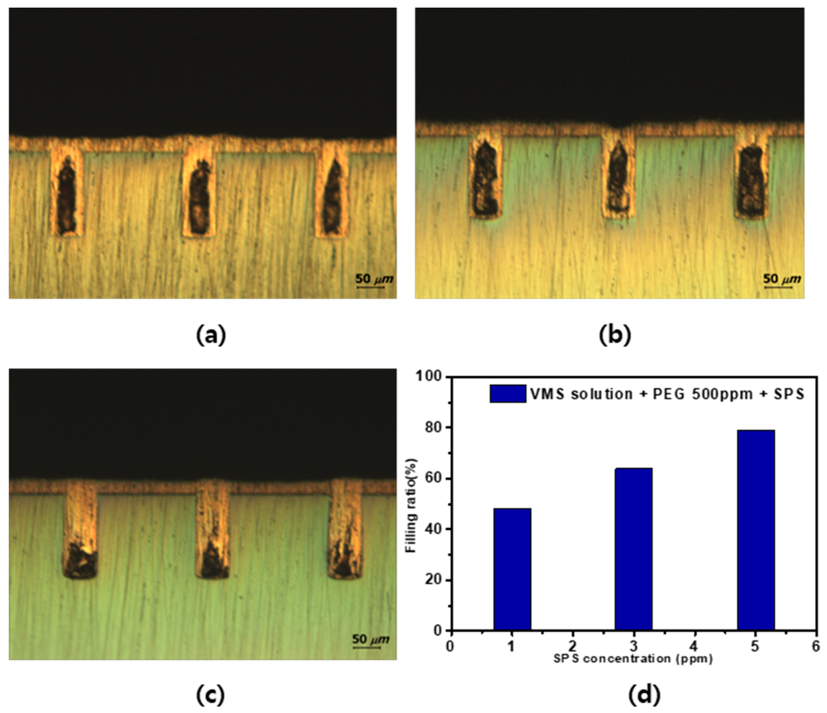
Figure 8.
(a–d) Images of changing JGB concentration in a VMS bath with 500 ppm PEG and 3 ppm SPS: (a) JGB 10 ppm, (b) JGB 20 ppm, (c) JGB 30 ppm, and (d) filling ratio graph for AR 1:3 TSV.
Figure 8.
(a–d) Images of changing JGB concentration in a VMS bath with 500 ppm PEG and 3 ppm SPS: (a) JGB 10 ppm, (b) JGB 20 ppm, (c) JGB 30 ppm, and (d) filling ratio graph for AR 1:3 TSV.

Figure 9.
Behavior of on-reverse current condition in electrodeposition.
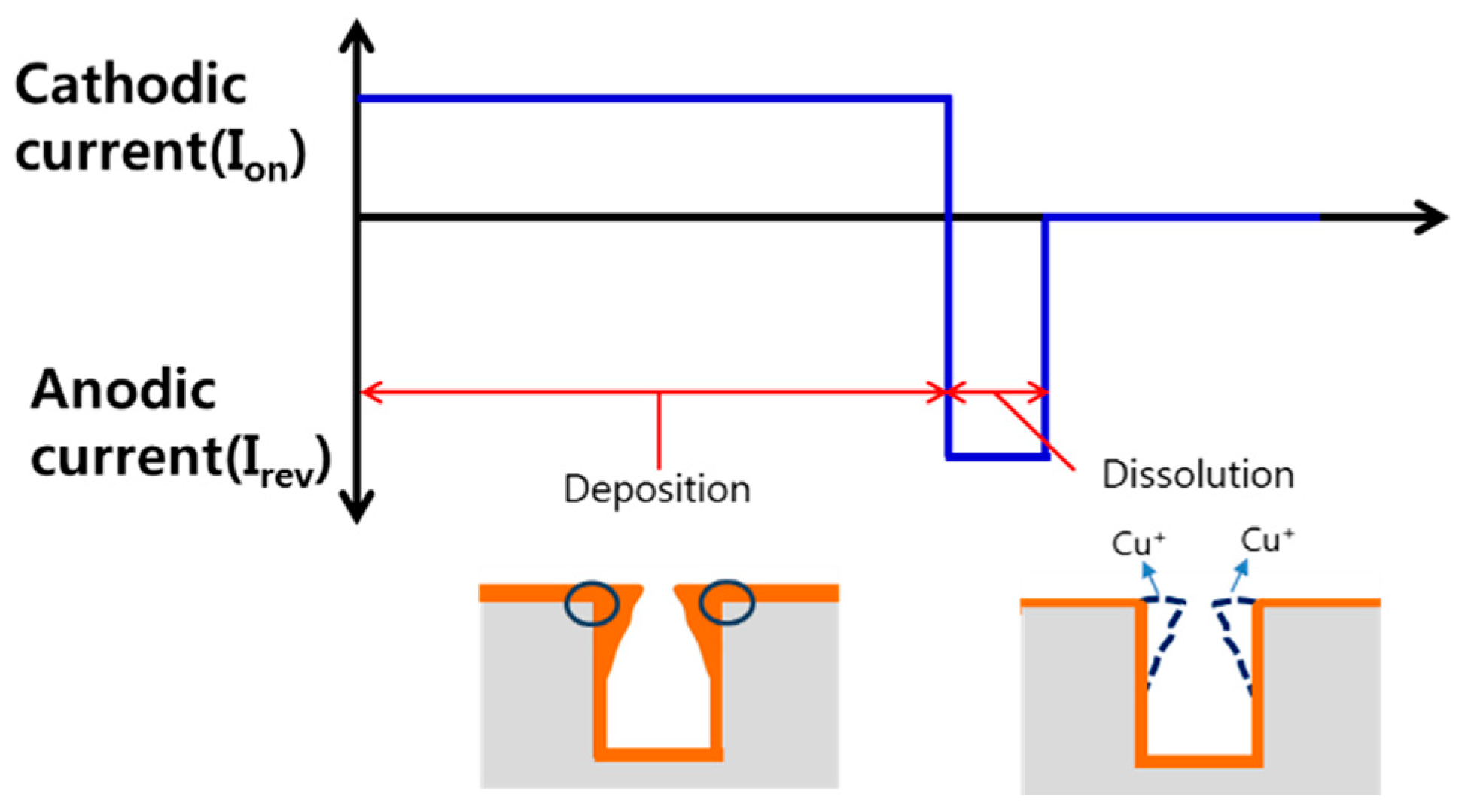
Figure 10.
Cross-sectional OM images and filling ratio graphs with changes in SPS concentration and reverse current conditions. (a–d) 8 mA, 16 mA, and 24 mA in SPS 3 ppm, respectively. (e–h) 8 mA/cm2, 16 mA/cm2, 24 mA/cm2 in SPS 5 ppm, respectively.
Figure 10.
Cross-sectional OM images and filling ratio graphs with changes in SPS concentration and reverse current conditions. (a–d) 8 mA, 16 mA, and 24 mA in SPS 3 ppm, respectively. (e–h) 8 mA/cm2, 16 mA/cm2, 24 mA/cm2 in SPS 5 ppm, respectively.

Figure 11.
SEM image of void-free filled TSV.

Table 1.
Composition of Cu bath.
| The Virgin Makeup Solution (VMS) | Additive | ||
|---|---|---|---|
| CuSO4·5H2O | 0.79 M | poly(ethylene glycol) (PEG) | 100–500 ppm |
| H2SO4 | 1.02 M | bis-(3-sodiumsulfopropyl disulfide) (SPS) | 1–5 ppm |
| Cl− | 1.4 mM | Janus Green B (JGB) | 10–50 ppm |
Table 2.
On-reverse current condition.
| On current | 10 mA/cm2 |
| Reverse current | 8, 16, 24 mA/cm2 |
| On time | 80 ms |
| Reverse time | 20 ms |
© 2018 by the authors. Licensee MDPI, Basel, Switzerland. This article is an open access article distributed under the terms and conditions of the Creative Commons Attribution (CC BY) license (http://creativecommons.org/licenses/by/4.0/).
Share and Cite
MDPI and ACS Style
Shin, S.-H.; Kim, T.-Y.; Park, J.-H.; Suh, S.-J. Optimization of Additive and Current Conditions for Void-Free Filled Through-Silicon Via. Appl. Sci. 2018, 8, 2135. https://doi.org/10.3390/app8112135
AMA Style
Shin S-H, Kim T-Y, Park J-H, Suh S-J. Optimization of Additive and Current Conditions for Void-Free Filled Through-Silicon Via. Applied Sciences. 2018; 8(11):2135. https://doi.org/10.3390/app8112135
Chicago/Turabian StyleShin, Se-Hee, Tea-Yoo Kim, Jong-Hwan Park, and Su-Jeong Suh. 2018. "Optimization of Additive and Current Conditions for Void-Free Filled Through-Silicon Via" Applied Sciences 8, no. 11: 2135. https://doi.org/10.3390/app8112135
Note that from the first issue of 2016, this journal uses article numbers instead of page numbers. See further details here.