Interface Growth and Void Formation in Sn/Cu and Sn0.7Cu/Cu Systems
by
Jieshi Chen
1,2, 
Yongzhi Zhang
3,
Zhishui Yu
1,2,
Peilei Zhang
1,2,
Wanqin Zhao
1,2,
Jin Yang
1,2,* and
Di Wu
1,2,* 1
School of Materials Engineering, Shanghai University of Engineering Science, Shanghai 201620, China
2
Shanghai Collaborative Innovation Center of Laser Advanced Manufacturing Technology, Shanghai 201620, China
3
AECC Commercial Aircraft Engine manufacturing CO., TLD., Shanghai 200241, China
*
Authors to whom correspondence should be addressed.
Appl. Sci. 2018, 8(12), 2703; https://doi.org/10.3390/app8122703
Submission received: 30 November 2018
/
Revised: 18 December 2018
/
Accepted: 18 December 2018
/
Published: 19 December 2018
(This article belongs to the Special Issue Selected Papers from the NMJ2018)
Abstract
:In this work, the effects of electroplated Cu (EP Cu) and Cu addition (0.7%) in Sn solder on the intermetallic compounds (IMCs) growth and void formation were clarified by comparison with solder joints comprising of high purity Cu (HP Cu) substrate and pure Sn solder. After aging processes, a new IMC, Cu3Sn, was formed at the interface, in addition to Cu6Sn5 formed in the as-soldered joints. The EP Cu and Cu addition (0.7%) both had limited effects on the total IMCs thickness. However, the effects varied on the growth behaviors of different IMCs. Comparing to the void-free interface between Sn and HP Cu, a large number of voids were observed at the Cu3Sn/Cu interface in Sn/EP Cu joints. The formation of these voids may be induced by the impurities and fine grain, which were introduced during the electroplating process. The addition of Cu suppressed the inter-diffusion of Cu and Sn at the interface. Consequently, the growth of the Cu3Sn layer and formation of voids were suppressed.
1. Introduction
Intermetallic compounds (IMCs) and voids that form at the interface between solder and copper joints have been given great attention, because the existence of these interfacial IMCs and voids are crucial to several reliability concerns [1,2]. Especially, the solder joints have been continuously scaled down due to the trends of microelectronic products from two-dimensional integration of circuits (2D IC) to three-dimensional integration of circuits (3D IC) [3]. IMCs’ growth and voids formed at the interfacial could induce more brittle fracture and impact fatigue failures [4,5].
In a Sn-Cu system, when the molten Sn-based solder alloy wets the Cu substrates, two different types of IMCs, e.g., Cu6Sn5 and Cu3Sn, form at the solder/Cu interface. Generally, the Cu6Sn5 layer was reported to be firstly formed at the liquid reaction stage, and becomes thicker with the solid state aging process. Later, a thin Cu3Sn layer is usually formed during the solid state aging process [6,7]. The Cu3Sn layer is usually formed during solid state aging process. Moreover, the formation of Cu3Sn would result in much bigger volume shrinkage relative to Cu6Sn5 [8,9]. As a result, Kirkendall voids (KVs) usually were observed at the Cu/Cu3Sn interface. It was reported that adding minor metallic (e.g., Ni, Ag, Cu, Zn, Al, Fe etc.) and ceramic (e.g., Al2O3, ZrO2, TiO2, SiC etc.) elements into the Sn-based solder could suppress the formation of voids and retard the growth of IMCs [10,11,12,13,14,15]. Cu is a basic element in the lead-free solder. Actually, recent research found that Cu also played an important role in reducing the thickness of the Cu3Sn IMC layer [16]. However, the mechanism of Cu addition retarding the growth of the Cu3Sn layer and void formation has not been clarified.
As we know, the Cu substrate in solders/Cu joint is made by the electroplating process. It is clearly different from high-purity Cu (HP Cu). Researchers points out that the voids are more prone to be formed in the Sn-based solder/EP Cu joints, relative to the Sn-based solder/HP Cu joints. Extensive research has been done on the effect of impurities of EP Cu on the formation of KVs [17,18,19]. Kim and Yu [17,18] clearly pointed out the detrimental effect of residual impurities in electroplated Cu UBM (under ball metal) on the void formation, and especially studied the effect of the S element. Liu et al. [19], proceeding from the source of impurities, systematically studied the influence of electroplating parameters on void formation at the interface. However, there have been few studies that explore the microstructure of Cu substrate. Zou et al. [20] mentioned that the formation of voids might be affected by the grain size of the Cu substrate.
In the present study, the HP Cu substrate, EP Cu substrate, and Sn0.7Cu solder were used to produce Sn/Cu joints. The effect of the microstructure of Cu substrates and Cu addition (0.7%) on the interface growth and void formation were analyzed. The interface evolution, especially the Kirkendall voiding level, was discussed.
2. Experimental Procedures
The solder used in this work was pure Sn (99.99%) and Sn0.7Cu (wt.%). Two kinds of substrates were introduced, high purity foil (99.99%, 0.1 mm in thickness) and electroplated Cu film (10 μm in thickness) deposited directly on the surface of the Cu foil. The electroplating solution contained CuSO4, H2SO4, HCl, and PEG (polyethylene glycol). The current density used during the electroplating process was 1.7 mA/cm2 [19]. The solder joints were prepared by melting Sn on the foils at 260 °C for 1 min. To investigate the interfacial microstructure in the solder joints, the isothermal aging for the as-reflowed samples was performed at 150 °C and 180 °C, respectively. Then, these samples were mounted in epoxy and metallurgically polished. The cross-sectional microstructure at the interface was observed by SEM (Sirion200), the compositions of the IMC layer were determined by energy dispersive spectroscopy (EDS), and the average thickness of IMC layers were measured with the software, Image J. X-ray photoelectron spectroscopy (XPS, AXIS UltraDLD) was used to characterize the presence of impurities (C, O, Cl, and S) in all kinds of Cu substrates. The average thickness of the IMC layer was calculated by dividing the IMC layer area by the length of the interface.
3. Results and Discussion
3.1. Sn/HP Cu and Sn/EP Cu Joints after Aging at 150 °C
The interfacial microstructure of Sn/HP Cu and Sn/EP Cu joints after aging at 150 °C with different aging periods are shown in Figure 1 and Figure 2. In all of the images, the upper, bottom, and middle materials are solder alloy, copper, and interfacial IMC layer, respectively. The chemical compositions of the IMC layers were characterized by EDS analysis.
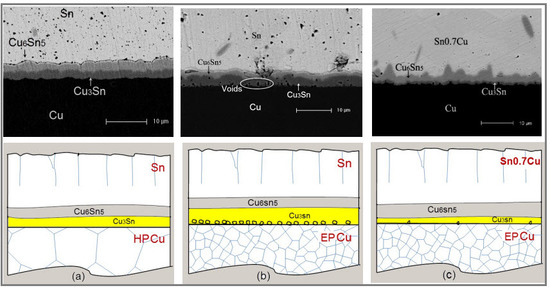
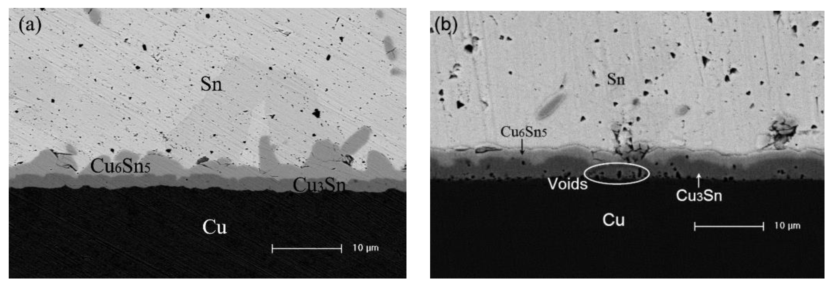
Figure 1a shows the interfacial microstructure of the as-reflowed Sn/HP Cu joint. A layer of scallop-shaped Cu6Sn5 formed at the interface, and no voids appeared at the interface. After aging at 150 °C for 240 h, a Cu3Sn layer emerged at the interface of Cu6Sn5/HP Cu, but no voids were detected, as presented in Figure 1b. Even after aging at 150 °C for 480 h, as seen in Figure 1c, no voids were observed at the Cu3Sn/HP Cu interface. Moreover, the thickness of the Cu3Sn layer grew rapidly, but the thickness of Cu6Sn5 layer seemed to remain constant.
The interfacial microstructure of the as-reflowed Sn/EP Cu joints can be observed in Figure 2a. Similar to the Sn/HP Cu joints, a scallop-shaped Cu6Sn5 layer formed at the interface and no voids were detected. After aging at 150 °C for 240 h, the total thickness of the IMC layers gradually increased in the Sn/EP Cu joints, and the Cu3Sn layer grew much faster than the Cu6Sn5 layer. Moreover, a certain number of voids were observed at the Cu3Sn/Cu interface, as seen in Figure 2b. When the aging time was extended to 480 h, the Cu6Sn5 layer thickness increased not obviously (Figure 2c). However, the thickness of the Cu3Sn layer became thicker with the rising aging time. Moreover, the size and number of voids were further increased at the Cu3Sn/Cu interface. In addition, the IMCs morphology became flattened, because Cu diffusion through the scallop valleys was faster than that through the scallop hills [21].
3.2. Sn0.7Cu/EP Cu Joints after Aging at 150 °C
Figure 3a shows the interfacial microstructures of as-reflowed Sn0.7Cu/EP Cu joints. Similar to the as-reflowed Sn/EP Cu joint, a thin layer of Cu6Sn5 was formed at the interface, and no void was observed in the sample. After a 240 h aging treatment at 150 °C, as shown in Figure 3b, the IMC layer thickness increased obviously. A thin Cu3Sn layer emerged between Cu6Sn5 and EP Cu. The thickness of the Cu3Sn layer was found to be sensitive to the Cu content. The addition of Cu could suppress the growth of the Cu3Sn layer. Also, several voids were found at the Cu3Sn/EP Cu interface in the Sn0.7Cu/EP Cu joint. Figure 3c presents the interfacial microstructures of the solder joints aged at 150 °C for 480 h. It was observed that the IMC layer continued to grow. However, lesser voids and a thinner Cu3Sn layer were found at the Sn0.7Cu/EP Cu interface than that of the Sn/EP Cu joint.
3.3. Sn/EP Cu Joints after Aging at 150 °C and 180 °C
The interfacial microstructure of the Sn/EP Cu joints with different aging conditions are shown in Figure 4. It was found that the voids did not appear at the Sn/EP Cu interface after aging at 150 °C for 120 h, as seen in Figure 4a, while a large number of voids was observed at the Cu3Sn/Cu interface in Sn/EP Cu aging at 180 °C after a short aging time (Figure 4b). In addition, the total thicknesses of the IMC layer were increased significantly after aging at 180 °C for 72 h, especially for the thickness of the Cu3Sn layer. Therefore, the temperature had significant influence on changing the growth rate of the voids and IMC layer; especially changing the reaction that occurred at the Cu6Sn5/Cu3Sn interface [13,22].
3.4. Growth Behaviors of IMC Layer
The thicknesses of the total IMCs, Cu6Sn5, and Cu3Sn layer for the three kinds of solder joints aged at different aging periods are shown in Figure 5. It was observed that the thickness of the total IMC layer increased with the aging time. EP Cu and Cu addition (0.7%) seemed to slightly affect the total IMC thickness. However, the growth behaviors of both the Cu6Sn5 and Cu3Sn layer were sensitive to the EP Cu and Sn0.7Cu solder. With the increase of the aging time, as presented in Figure 5b, the thickness of the Cu6Sn5 layer in the Sn/HP Cu joints was relatively stable, while the thickness of the Cu6Sn5 layer in the Sn/EP Cu joints was decreased. The thickness of the Cu6Sn5 layer in the Sn0.7Cu/EP Cu joints gradually increased. For the thickness of the Cu3Sn layer, as seen in Figure 5c, it was observed that the thickness of the Cu3Sn layer increased with the aging time. The growth rate of the Cu3Sn layer in the Sn/EP Cu joint was larger than that of Sn/HP Cu. While in the Sn0.7Cu/EP Cu joint, the growth rate of the Cu3Sn layer slowed down. This suggested that the EP Cu substrate promoted growth of the Cu3Sn layer, while Cu addition (0.7%) had the function of suppressing growth of the Cu3Sn layer.
Yoon et al. [13] investigated the effects of Cu on the interfacial reaction of Sn-Ag/Cu solder joints. They also found that increasing the amount of Cu in Sn-Ag solder significantly reduced the thickness of the Cu3Sn layer. The proportion of Cu6Sn5 vs Cu3Sn in the Sn-3.0Ag-0.5Cu/Cu solder joint after aging at 150 °C for 28 days was about 6:4. On other hand, a Cu6Sn5/Cu3Sn ratio of about 7:3 was observed in the Sn-3.0Ag-1.0Cu/Cu joint. In addition, Choi et al. [22] studied IMC growth in Sn-Ag/Cu solder joints. They found that the thickness ratio of Cu6Sn5 to Cu3Sn was about 2:1 as aged at 150 °C for 700 h. In our work, the Cu6Sn5/Cu3Sn ratios were 1:1 in the Sn/HP Cu solder joint, 1:6 in the Sn/EP Cu, and 2:1 in the Sn0.7Cu/EP Cu as aged at 150 °C for 480 h. The results indicated that the EP Cu substrate promotes growth of the Cu3Sn layer, and Cu addition (0.7%) is beneficial in retarding the growth of the Cu3Sn layer.
As the temperature increased to 180 °C, as seen in Figure 5d, it was observed that the thickness of the total IMC layer of Sn/EP Cu increased with the aging temperature, and the Cu6Sn5/Cu3Sn ratio was 1:6 in the Sn/ EP Cu as aged at 150 °C for 480 h, and 1:8 in the Sn/ EP Cu was aged at 180 °C for 480 h. The results indicated that aging temperature could change the reaction occurring at the Cu6Sn5/Cu3Sn interface.
3.5. Discussion
According to the results obtained, the voids did not appear at the Sn/HP Cu interface, while they formed at the Sn/EP Cu interfaces. This implied that EP Cu may be the main cause for the formation of voids. In the process of electroplating, a number of impurities and defects were introduced into the deposited Cu film [23]. Impurity elements, such as C, O, Cl, and S, existed in the EP Cu based on XPS analysis, as seen in Figure 6. Lee and Park [23] reported that the organic impurity, poly ethylene glycol (PEG-), was absorbed at the grain boundary of EP Cu film. Yu et al. [18] showed that the segregation of impurities (like S) to the Cu/Cu3Sn interface might lower the nucleation energy of KVs, facilitating the formation and growth of Kirkendall voids. As seen in Figure 2, during the thermal aging, the Cu3Sn/EP Cu interface shifted towards the substrate gradually through the consumption of Cu film. The impurities contained in the film would involve the reaction interface. The Cu3Sn/EP Cu interface was the most active area for the voiding, which also served as the heterogeneous sites. Therefore, all evidence indicates that the impurities are obviously a dominant reason for voiding. Moreover, according to the experimental results, it was found that the voiding level increases with growth of the Cu3Sn layer.
For the Sn-Cu system, the chemical reactions at the Cu/Cu3Sn and Cu3Sn/Cu6Sn5 interfaces were represented by chemical equations [24].
At the Cu/Cu3Sn interface on the Cu3Sn side (the elements in square brackets denote the diffusing species):
At the Cu3Sn/Cu6Sn5 interface on the Cu3Sn side:
At the Cu3Sn/Cu6Sn5 interface on the Cu6Sn5 side:
According to the equations above, the interfacial reaction was a dynamic process. At the Cu3Sn/Cu6Sn5 interface, the reaction direction in Equations (2) and (3) was opposite to that in Equations (4) and (5). The final reaction direction, i.e., the migration direction of the Cu3Sn/Cu6Sn5 interface, was determined, to a large extent, by the diffusion fluxes of Cu and Sn. It is well known that copper was the dominant diffusing species in the Sn/Cu reaction couple [25]. The grain boundary diffusion was a dominant diffusion mechanism for the Cu atom [26]. We plotted some sketch maps reflecting the relation between interface behavior and high-purity Cu (HP Cu), electroplated Cu (EP Cu) and Cu addition (0.7%), respectively, based on the experimental results, as shown in Figure 7. I was observed that EP Cu was smaller in grain size than that of HP Cu. It is known to all that finer grained Cu film could supply much more diffusion paths for Cu atom diffusion, resulting in a bigger atom flux shifting out of the interface. Hence, a much bigger Cu flux would be generated in the EP Cu. This was favorable for the reactions on the Cu3Sn side (Equation (2) and Equation (3)). In addition, according to Equation Jv = JCu − JSn, the finer EP Cu was able to supply a bigger JCu due to more diffusion paths, which was expected to generate more considerable vacancies at the EP Cu/IMC interface, relative to the HP Cu/IMC. At last, the vacancies gathered together to form the micro voids, or KVs.
The Cu element in the solder likely lowered the Cu concentration gradient at the solder/Cu interface, and suppressed the diffusion of Cu atoms from the Cu substrate to the solder [27]. The declined Cu flux not only reduced the consumption of Cu substrate (Equation (1)), but also was favorable for the reactions on the Cu6Sn5 side (Equation (4) and Equation (5)). Therefore, the growth of the Cu3Sn layer was retarded at both sides. Besides, the lesser the consumption of the Cu substrate, the fewer impurities incorporated into the reaction interface. Consequently, fewer voids were formed.
4. Conclusions
In this work, the interface growth and void formation in the Sn/Cu as-reflowed joints and aged joints were comparatively studied in the combination of pure Sn solder and HP Cu substrate, pure Sn solder and EP Cu substrate as well as Cu addition (0.7%) of Sn solder and EP Cu substrate. The EP Cu and Cu addition (0.7%) seemed to slightly affect the total IMCs thickness. However, they showed different effects on the growth behaviors of different IMCs, i.e., Cu6Sn5 and Cu3Sn. The EP Cu substrate significantly suppressed the growth of the Cu6Sn5 layer; while it promoted the growth of the Cu3Sn layer. In the case of Cu addition (0.7%), it had the function of suppressing growth of the Cu3Sn layer, but retarded the growth of the Cu3Sn layer. During the thermal aging, a number of voids appeared at the Cu3Sn/Cu interface in Sn/EP Cu joints, but not in Sn/HP Cu joints. These voids could be mainly caused by the impurities and fine grain incorporated during electroplating. The addition of Cu element (0.7 wt.%) retarded the growth of the Cu3Sn layer and suppressed the formation of voids.
Author Contributions
J.C. conceived and performed the experiments, analyzed the data, and wrote the paper. Y.Z. and Z.Y. provided the experimental materials and laboratory equipment, and directed the research. W.Z., D.W., J.Y. and P.Z. contributed to the discussion and interpretation of the results.
Acknowledgements
This project is supported by National Natural Science Foundation of China (Grant Nos.51805316, 51805315 and 51605276), Shanghai Science and Technology Development Funds (18FY1424900) and Shanghai Science and Technology Committee Innovation Grant (17JC1400600, 17JC1400601).
Conflicts of Interest
The authors declare no conflicts of interest.
References
- Tu, K.N.; Hsiao, H.Y.; Chen, C. Transition from flip chip solder joint to 3D IC micro-bump: Its effect on microstructure anisotropy. Microelectron. Reliab. 2013, 53, 2–6. [Google Scholar] [CrossRef]
- Che, F.X.; Pang, H.L.J. Characterization of IMC layer and its effect on thermomechanical fatigue life of Sn–3.8 Ag–0.7 Cu solder joints. J. Alloys Compd. 2012, 541, 6–13. [Google Scholar] [CrossRef]
- Chen, K.; Kunz, M.; Tamura, N.; Wenk, H.R. Residual stress preserved in quartz from the San Andreas Fault Observatory at Depth. Geology 2015, 43, 219–222. [Google Scholar] [CrossRef] [Green Version]
- Zeng, K.; Tu, K.N. Six cases of reliability study of Pb-free solder joints in electronic packaging technology. Mater. Sci. Eng. R Rep. 2002, 38, 55–105. [Google Scholar] [CrossRef]
- Tu, K.N.; Zeng, K. Tin–lead (SnPb) solder reaction in flip chip technology. Mat. Sci. Eng. R Rep. 2001, 34, 1–58. [Google Scholar] [CrossRef]
- Tsao, L.C. Suppressing effect of 0.5 wt.% nano-TiO2 addition into Sn–3.5Ag–0.5Cu solder alloy on the intermetallic growth with Cu substrate during isothermal aging. J. Alloys Compd. 2011, 509, 8441–8448. [Google Scholar] [CrossRef]
- Gain, A.K.; Chan, Y.C. Growth mechanism of intermetallic compounds and damping properties of Sn–Ag–Cu-1wt% nano-ZrO2 composite solders. Microelectron. Reliab. 2014, 54, 945–955. [Google Scholar] [CrossRef]
- Song, J.Y.; Yu, J.; Lee, T.Y. Effects of reactive diffusion on stress evolution in Cu–Sn films. Scr. Mater. 2004, 51, 167–170. [Google Scholar] [CrossRef]
- Buchovecky, E.; Jadhav, N.; Bower, A.F.; Chason, E. Finite element modeling of stress evolution in Sn films due to growth of the Cu6Sn5 intermetallic compound. J. Electron. Mater. 2009, 38, 2676–2684. [Google Scholar] [CrossRef]
- Yen, Y.W.; Lin, C.Y.; Hermana, G.N.; Chen, P.Y.; Wu, Y.P. Interfacial reactions in the Au/Sn-xZn/Cu sandwich couples. J. Alloys Compd. 2017, 710, 479–490. [Google Scholar] [CrossRef]
- Zeng, G.; McDonald, S.D.; Gu, Q.; Terada, Y.; Uesugi, K.; Yasuda, H.; Nogita, K. The influence of Ni and Zn additions on microstructure and phase transformations in Sn–0.7 Cu/Cu solder joints. Acta Mater. 2015, 83, 357–371. [Google Scholar] [CrossRef]
- Wang, Y.W.; Lin, Y.W.; Tu, C.T.; Kao, C.R. Effects of minor Fe, Co, and Ni additions on the reaction between SnAgCu solder and Cu. J. Alloys Compd. 2009, 478, 121–127. [Google Scholar] [CrossRef]
- Yoon, J.W.; Noh, B.I.; Jung, S.B. Effects of third element and surface finish on interfacial reactions of Sn–Ag–xCu (or Ni)/(Cu or ENIG) solder joints. J. Alloys Compd. 2010, 506, 331–337. [Google Scholar] [CrossRef]
- Zhang, L.; Tu, K.N. Structure and properties of lead-free solders bearing micro and nano particles. Mater. Sci. Eng. R Rep. 2014, 82, 1–32. [Google Scholar] [CrossRef]
- Kotadia, H.R.; Howes, P.D.; Mannan, S.H. A review: On the development of low melting temperature Pb-free solders. Microelectron. Reliab. 2014, 54, 1253–1273. [Google Scholar] [CrossRef]
- Yu, C.; Chen, J.S.; Wang, K.Y.; Chen, J.Q.; Lu, H. Suppression effect of Cu and Ag on Cu3Sn layer in solder joints. J. Mater. Sci. Mater. Electron. 2013, 24, 4630–4635. [Google Scholar] [CrossRef]
- Kim, J.Y.; Yu, J.; Kim, S.H. Effects of sulfide-forming element additions on the Kirkendall void formation and drop impact reliability of Cu/Sn–3.5 Ag solder joints. Acta Mater. 2009, 57, 5001–5012. [Google Scholar] [CrossRef]
- Yu, J.; Kim, J.Y. Effects of residual S on Kirkendall void formation at Cu/Sn–3.5 Ag solder joints. Acta Mater. 2008, 56, 5514–5523. [Google Scholar] [CrossRef]
- Liu, Y.; Wang, J.; Yin, L.; Kondos, P.; Parks, C.; Borgesen, P.; Dimitrov, N. Influence of plating parameters and solution chemistry on the voiding propensity at electroplated copper–solder interface. J. Appl. Electrochem. 2008, 38, 1695–1705. [Google Scholar] [CrossRef]
- Zou, J.; Mo, L.; Wu, F.; Wang, B.; Liu, H.; Zhang, J.; Wu, Y. Effect of Cu substrate and solder alloy on the formation of kirkendall voids in the solder joints during thermal aging. In Proceedings of the 2010 11th International Conference on Electronic Packaging Technology & High Density Packaging (ICEPT-HDP), Xi’an, China, 16–19 August 2010; pp. 944–948. [Google Scholar]
- Zou, H.F.; Yang, H.J.; Zhang, Z.F. Morphologies, orientation relationships and evolution of Cu6Sn5 grains formed between molten Sn and Cu single crystals. Acta Mater. 2008, 56, 2649–2662. [Google Scholar] [CrossRef]
- Choi, S.; Bieler, T.R.; Lucas, J.P.; Subramanian, K.N. Characterization of the growth of intermetallic interfacial layers of Sn-Ag and Sn-Pb eutectic solders and their composite solders on Cu substrate during isothermal long-term aging. J. Electron. Mater. 1999, 28, 1209–1215. [Google Scholar] [CrossRef]
- Lee, C.H.; Park, C.O. Residual stress effect on self-annealing of electroplated copper. Jpn. J. Appl. Phys. 2003, 42, 4484–4488. [Google Scholar] [CrossRef]
- Yang, Y.; Lu, H.; Yu, C. Void formation at the interface in Sn/Cu solder joints. Microelectron. Reliab. 2011, 51, 2314–2318. [Google Scholar] [CrossRef]
- Kim, S.; Yu, J. Recrystallization-induced void migration in electroplated Cu films. Scr. Mater. 2012, 67, 312–315. [Google Scholar] [CrossRef]
- Jung, K.; Conrad, H. Retardation of grain growth in electrodeposited Cu by an electric field. J. Mater. Sci. 2007, 42, 3994–4003. [Google Scholar] [CrossRef]
- Wang, Y.W.; Lin, Y.W.; Kao, C.R. Inhibiting the formation of microvoids in Cu3Sn by additions of Cu to solders. J. Alloys Compd. 2010, 493, 233–239. [Google Scholar] [CrossRef]
Figure 1.
Interfacial microstructure of Sn/HP Cu joints after aging at 150 °C for (a) 0 h, (b) 240 h, and (c) 480 h.
Figure 1.
Interfacial microstructure of Sn/HP Cu joints after aging at 150 °C for (a) 0 h, (b) 240 h, and (c) 480 h.

Figure 2.
Interfacial microstructure of Sn/EP Cu joints after aging at 150 °C for (a) 0 h, (b) 240 h, and (c) 480 h.
Figure 2.
Interfacial microstructure of Sn/EP Cu joints after aging at 150 °C for (a) 0 h, (b) 240 h, and (c) 480 h.

Figure 3.
Interfacial microstructure of Sn0.7Cu/EP Cu joints after aging at 150 °C for (a) 0 h, (b) 240 h, and (c) 480 h.
Figure 3.
Interfacial microstructure of Sn0.7Cu/EP Cu joints after aging at 150 °C for (a) 0 h, (b) 240 h, and (c) 480 h.

Figure 4.
Interfacial microstructure of Sn/EP Cu joints with different aging conditions, (a) 150 °C for 120 h, (b) 180 °C for 72 h.
Figure 4.
Interfacial microstructure of Sn/EP Cu joints with different aging conditions, (a) 150 °C for 120 h, (b) 180 °C for 72 h.

Figure 5.
Relationship between aging time and average thickness of total IMCs (a), Cu6Sn5 (b), and Cu3Sn (c) layer for the three kinds of solder joints after aging at 150 °C and 180 °C (d), respectively.
Figure 5.
Relationship between aging time and average thickness of total IMCs (a), Cu6Sn5 (b), and Cu3Sn (c) layer for the three kinds of solder joints after aging at 150 °C and 180 °C (d), respectively.

Figure 6.
The components of EP Cu substrates by XPS spectra.

Figure 7.
Schematic drawings showing the general process for interfacial behavior in Sn/HP Cu (a), Sn/EP Cu (b), and Sn0.7Cu/EP Cu (c) systems.
Figure 7.
Schematic drawings showing the general process for interfacial behavior in Sn/HP Cu (a), Sn/EP Cu (b), and Sn0.7Cu/EP Cu (c) systems.

© 2018 by the authors. Licensee MDPI, Basel, Switzerland. This article is an open access article distributed under the terms and conditions of the Creative Commons Attribution (CC BY) license (http://creativecommons.org/licenses/by/4.0/).
Share and Cite
MDPI and ACS Style
Chen, J.; Zhang, Y.; Yu, Z.; Zhang, P.; Zhao, W.; Yang, J.; Wu, D. Interface Growth and Void Formation in Sn/Cu and Sn0.7Cu/Cu Systems. Appl. Sci. 2018, 8, 2703. https://doi.org/10.3390/app8122703
AMA Style
Chen J, Zhang Y, Yu Z, Zhang P, Zhao W, Yang J, Wu D. Interface Growth and Void Formation in Sn/Cu and Sn0.7Cu/Cu Systems. Applied Sciences. 2018; 8(12):2703. https://doi.org/10.3390/app8122703
Chicago/Turabian StyleChen, Jieshi, Yongzhi Zhang, Zhishui Yu, Peilei Zhang, Wanqin Zhao, Jin Yang, and Di Wu. 2018. "Interface Growth and Void Formation in Sn/Cu and Sn0.7Cu/Cu Systems" Applied Sciences 8, no. 12: 2703. https://doi.org/10.3390/app8122703
Note that from the first issue of 2016, this journal uses article numbers instead of page numbers. See further details here.