Article

Photo-Excited Metasurface for Tunable Terahertz Reflective Circular Polarization Conversion and Anomalous Beam Deflection at Two Frequencies Independently

1
School of Information Science and Engineering, Wuhan University of Science and Technology, Wuhan 430081, China
2
Engineering Research Center for Metallurgical Automation and Detecting Technology Ministry of Education, Wuhan University of Science and Technology, Wuhan 430081, China
3
Hubei Longzhong Laboratory, Xiangyang 441000, China
4
School of Physics and Electronic Information Engineering, Hubei Engineering University, Xiaogan 432000, China
*
Author to whom correspondence should be addressed.
Nanomaterials 2023, 13(12), 1846; https://doi.org/10.3390/nano13121846
Submission received: 15 May 2023 / Revised: 8 June 2023 / Accepted: 10 June 2023 / Published: 12 June 2023
(This article belongs to the Special Issue Advanced Nanomaterials in Terahertz and Microwave Technology)

Abstract

:
In this paper, a photo-excited metasurface (MS) based on hybrid patterned photoconductive silicon (Si) structures was proposed in the terahertz (THz) region, which can realize the tunable reflective circular polarization (CP) conversion and beam deflection effect at two frequencies independently. The unit cell of the proposed MS consists of a metal circular-ring (CR), Si ellipse-shaped-patch (ESP) and circular-double-split-ring (CDSR) structure, a middle dielectric substrate, and a bottom metal ground plane. By altering the external infrared-beam pumping power, it is possible to modify the electric conductivity of both the Si ESP and CDSR components. By varying the conductivity of the Si array in this manner, the proposed MS can achieve a reflective CP conversion efficiency that ranges from 0% to 96.6% at a lower frequency of 0.65 THz, and from 0% to 89.3% at a higher frequency of 1.37 THz. Furthermore, the corresponding modulation depth of this MS is as high as 96.6% and 89.3% at two distinct and independent frequencies, respectively. Moreover, at the lower and higher frequencies, the 2π phase shift can also be achieved by respectively rotating the oriented angle (αi) of the Si ESP and CDSR structures. Finally, an MS supercell is constructed for the reflective CP beam deflection, and the efficiency is dynamically tuned from 0% to 99% at the two independent frequencies. Due to its excellent photo-excited response, the proposed MS may find potential applications in active functional THz wavefront devices, such as modulators, switches, and deflectors.

1. Introduction

Terahertz (THz) radiation pertains to electromagnetic (EM) waves within the frequency range of 0.1 THz to 10 THz. In comparison to X-rays and microwaves, THz radiation exhibits a smaller single photon energy and a more diverse spectral range. Consequently, the technologies and applications derived from THz radiation have tremendous potential for development in several fields [1], such as biomedicine [2,3,4], astronomy [5], and next-generation wireless communications [6]. Nevertheless, progress in the development of THz technologies and applications has been limited due to the difficulty of naturally occurring matter producing an efficient EM response to THz waves [7,8]. In the past few years, the THz frequency range was once known as the “THz Gap” [9]. However, with the advent of EM metamaterials (MMs) [10,11,12,13], the research in THz technologies and applications has gained significant traction. MMs are man-made materials that consist of artificially designed microcellular structures arranged in specific arrangements. Despite being composed of natural materials at their core, MMs can achieve a series of EM wave modulation phenomena that the scope of natural materials cannot achieve, such as negative refraction [14,15], imaging [16,17], transformation optics [18], perfect absorption [19], and deflection [20,21], among others.
To overcome the limitations of high loss, large size, and complex fabrication techniques associated with three-dimensional (3D) MM themselves [22], researchers have developed two-dimensional (2D) ultrathin arrays, called metasurfaces (MSs) [23,24,25]. Compared to MMs, MSs offer the advantage of being lighter, thinner, and easier to fabricate, while also providing more flexible modulation of THz waves. Thus, various THz devices with single or composite functions, such as abnormal refraction/reflection, perfect absorption, beam splitters, orbital angular momentum, polarization conversion, beam deflection, and so on, have been proposed intensively [26,27,28,29,30,31,32,33,34,35,36,37,38,39,40,41]. Among these functions, polarization conversion and beam deflection are some of the most fundamental functionalities in photoelectric information processing systems. In recent years, a large number of MSs from microwave to even visible frequencies have been proposed and investigated intensively, which can be functioned as various polarization converters and beam deflectors [33,34,35,36,42,43]. For example, Zhao et al., proposed a transmission-type MS based on bilayer metallic patches, which functioned as a high-efficiency THz beam deflector [33]. Cheng et al., designed a tri-band high-efficiency circular-polarization (CP) converter based on a tri-layer split-ring structure, which can convert the incident CP wave to its orthogonal component after transmission [34]. Liu et al., demonstrated a novel design of a deeply subwavelength structure, which was constructed as a THz reflective beam deflector [35]. Jia et al., proposed an achromatic dielectric MS, which demonstrated an achromatic feasibility of the beam deflector from 0.6 to 1.2 THz [36]. Although the THz MSs can achieve the polarization conversion or beam deflection function, most functionalities are fixed and unchangeable once they are designed and fabricated, thus restricting their scope of application. As the application blooms increasingly, developing tunable MSs is necessary and highly desirable [44,45,46,47,48,49]. Ha et al., proposed a new strategy for on-chip planar compact MS made of gold and phase-change material GST, which can achieve a continuous beam-steering at 10.6 μm [46]. Kim et al., proposed an innovative approach for designing a nanophotonic beam deflector with superior performance characteristics, including broadband operation, extensive active tunability, and high signal efficiency, all achieved simultaneously [47]. Yu et al., proposed a novel and reconfigurable MS capable of dynamically switching the deflection angles in the opposite direction, while also exhibiting an impressive relative bandwidth of up to 47.6% for achromatic reflection in the microwave region [48]. Recently, photoconductive Si has increasingly received great attention due to its active tunable behavior of the electric conductivity induced by external optical pumping power [49]. The photoconductive Si can be used to construct the various MS devices with tunable functions in the THz region [49,50,51,52,53,54,55,56,57,58,59], such as absorbers, switchers, and polarization converters. The patterned photoconductive Si is usually embedded in or combined with the metal resonator to form a hybrid structure for dynamically manipulating the THz wave, which can be prepared and fabricated easily using standard lithography and E-beam evaporation technology [49,55,56]. The electric response of the patterned photoconductive Si is determined by the infrared pumping power. However, photoconductive Si-based tunable MSs with functionalities such as polarization conversion and beam deflection have not been studied yet.
In this work, we have designed and demonstrated a photo-excited THz tunable MS based on hybrid structures of photoconductive Si ellipse-shaped patch (ESP) and circular double split ring (CDSR) and metal circular ring (CR), which can be used to construct a tunable reflective CP converter and a beam deflector, respectively. Since the conductivity of the patterned Si structures can be adjusted by changing the optical-pump power, the proposed MSs can realize a continuous modulation of the efficiency of the CP conversion and deflection at two independent THz frequency ranges. Firstly, the reflection CP conversion property of the proposed MS was demonstrated numerically under the upper optical-pump power. The physics origin of the proposed MS structures was illustrated by analyzing the electric field and surface current distributions on the unit cell at two different frequencies. Then, by respectively rotating the azimuth rotation angles (α1 and α2) of the Si CDSR and ESP structures, 0–2π phase shift of the reflection orthogonal CP waves could be obtained around 0.65 THz and 1.37 THz, respectively. Thirdly, a tunable MS reflective-beam deflector with a linear phase gradient was proposed and demonstrated numerically. This optically tunable reflective-mode MS may find more exciting applications, such as polarization converters, modulators, and beam deflectors.

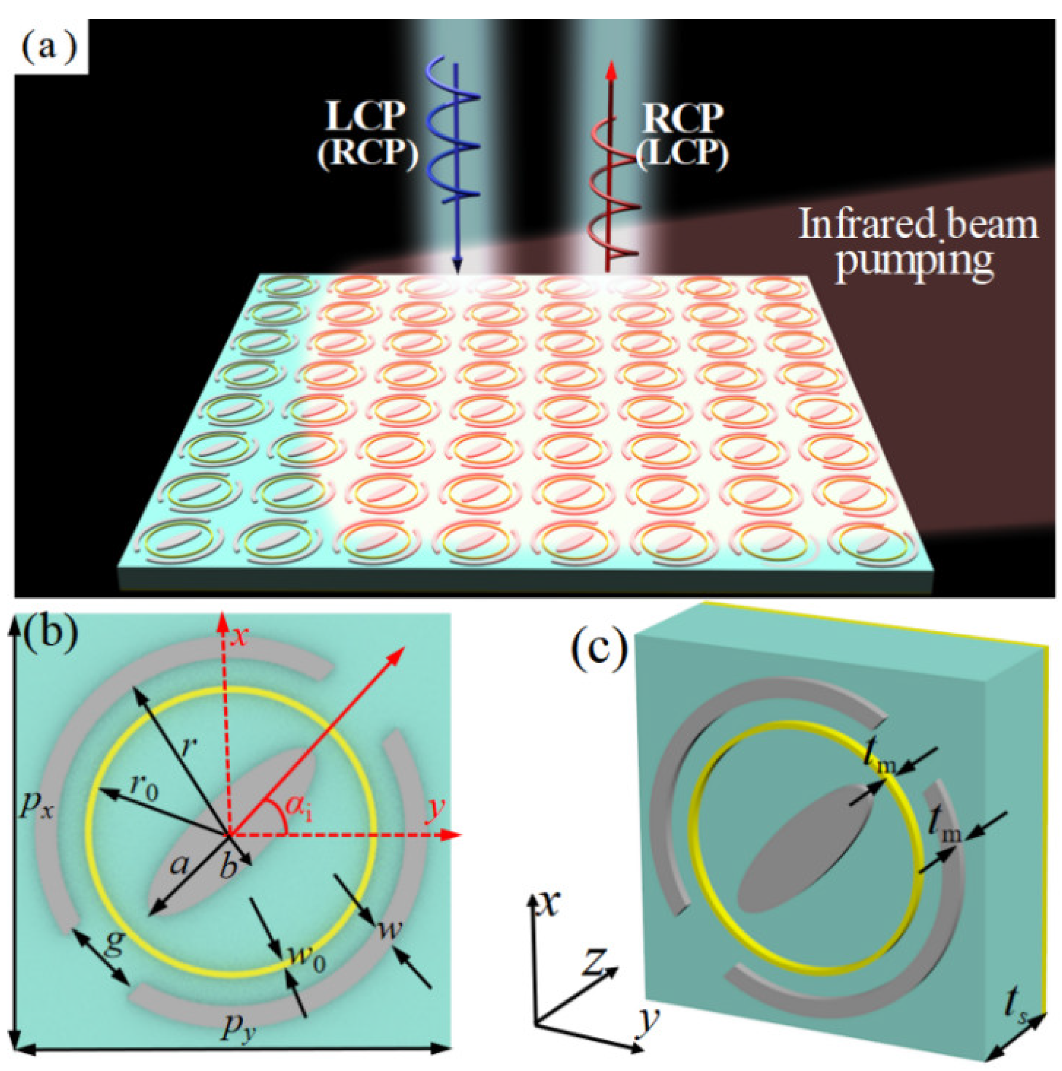
2. Structure Design and Simulations

Figure 1 illustrates the scheme of the proposed photo-excited THz tunable MS. As shown in Figure 1b,c, the unit cell of the proposed photo-excited MS is composed of hybrid structures of Si ESP and CDSR and metal CR, a middle dielectric substrate, and a metal ground plane. The top and bottom layers of the proposed MS structure can form a Fabry–Pérot-like resonance cavity, resulting in a highly efficient polarization conversion through the multiple interference effect [43,53]. In addition, the symmetry axis of ESP and CDSR structures of the proposed MS is rotated αi (i = 1, 2) along the x(y)-axis direction, indicating a typical anisotropy in the x-y plane. This anisotropic design is also very key to achieving reflective polarization conversion [36,60,61,62,63]. Note that the two distinct resonators (Si ESP and CDSR structure) are responsible for manipulating the THz wave at two corresponding frequencies independently. The sequence arrangement of discrete ESP and CDSR structures will inevitably lead to cross-coupling effects, which will cause some discrepancies between the designed phase and the practical arranged phase, thus finally resulting in a reduction of MS device efficiency [31,32]. In our design, the metal CR structure is added and used to reduce the cross-talk and cross-coupling effect between the ESP and CDSR structures. By constantly changing the radius of the metal CR, we ultimately controlled the impact to a low degree. Thus, it can be expected that the designed MS can independently control the reflective beams at two different THz frequency regions.
The electric conductivity of the photoconductive Si is usually proportional to the pumping power of the incident infrared light [49,50]. For example, the conductivity of the photoconductive Si is only about 1 S/m without infrared pumping (power is zero), while the one is about 1.5 × 10⁵ S/m under the upper-limiting infrared pumping (central wavelength of 800 nm and power is about 405 mJ/cm2) [49,50,55]. As shown in Figure 1a, an excess carrier density will be generated as long as the pumping energy exceeds the band-gap energy of the photoconductive Si when an infrared beam is illuminated on the designed MS [49,50]. In this case, the hybrid structures of the photoconductive Si array are in the metal state. While without infrared illumination, the hybrid structures of the photoconductive Si are in the insulation state. Note that the entire area of the designed MS is fully covered by the infrared beam (see Figure 1a).
As is well known, the geometric phase, also named Pancharatnam–Berry (PB) phase, has the obvious advantage of being nondispersive of the MS unit cell. The spatial asymmetry of the MS unit cell will lead to the anisotropy of the polarized wave. The oriented angles (α1 and α2) of the designed MS exhibit spatially dependent optical axis distribution, which will bring the additional phase difference φ to the two orthogonal CP components. According to the PB principle, the relationship between the oriented angles (α1 and α2) of the structural photoconductive Si and the additional phase φ can be expressed by φi = 2σαi, where σ = ±1 corresponds to the helicity direction for the CP wave [26], e.g., left-handed or right-handed CP (“+” RCP, or “−” LCP). Consequently, the continuous 2π phase shift can be easily achieved by rotating the αi (i = 1, 2) instead of changing the structure parameter of the MS unit cell.
To demonstrate the functions of the designed MS, a full wave simulation was carried out using the frequency solver by the CST Microwave Studio based on the finite element method (FEM). In the simulation, the Floquet ports for the incident THz CP plane waves along the z-axis direction are assigned to the unit cell of the proposed MS structure. In addition, the distance between the wave ports and the unit-cell structure is 300 μm in order to only get enough propagating information of the reflected THz wave. In addition, the minimized mesh size is set as 0.22 μm, which is much smaller than the unit-cell size and the operating wavelength. During the optimization process, the main objective is to get the maximized magnitude of the reflected orthogonal CP wave at two distinct THz frequency ranges when the designed MS is under the upper infrared pumping power (σsi = 1.5 × 10⁵ S/m). The hybrid structure of photoconductive Si was modeled as a dielectric with a relative permittivity of εSi = 11.7, while the electrical conductivity σSi is dependent on external infrared beam power in our interested THz frequency range [49,50]. The metal CR structure and ground plane of the MS are made of a copper film with conductivity σ = 5.8 × 10⁷ S/m. The low-loss polyimide with a permittivity of 2.35 × (1 + i × 0.0027) was chosen as the middle dielectric substrate layer. After simulation optimization, the final geometrical parameters of the unit cell are given as px = py = 100 μm, a = 26 μm, b = 8 μm, r = 40 μm, w = 5 μm, g = 20 μm, tm = 3 μm, r0 = 33.5 μm, w0 = 1.5 μm, and ts = 35 μm. In addition, the orientations of the outer CDSR and inner ESP are denoted as α1 and α2 with respect to the x/(y)-axis, respectively.

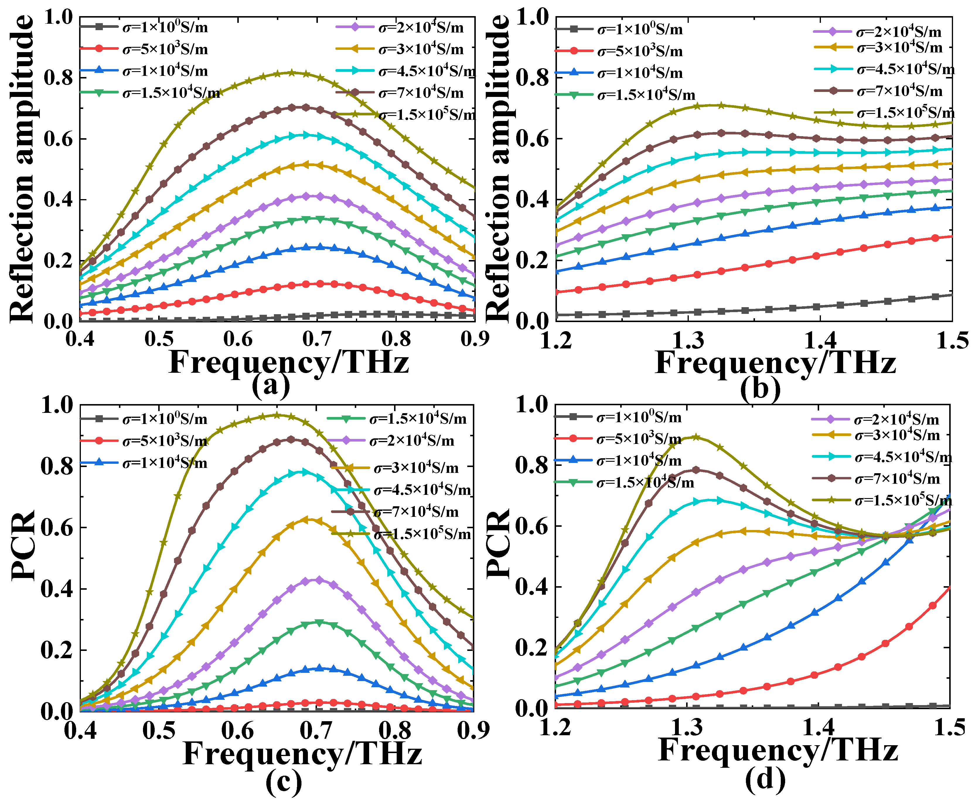
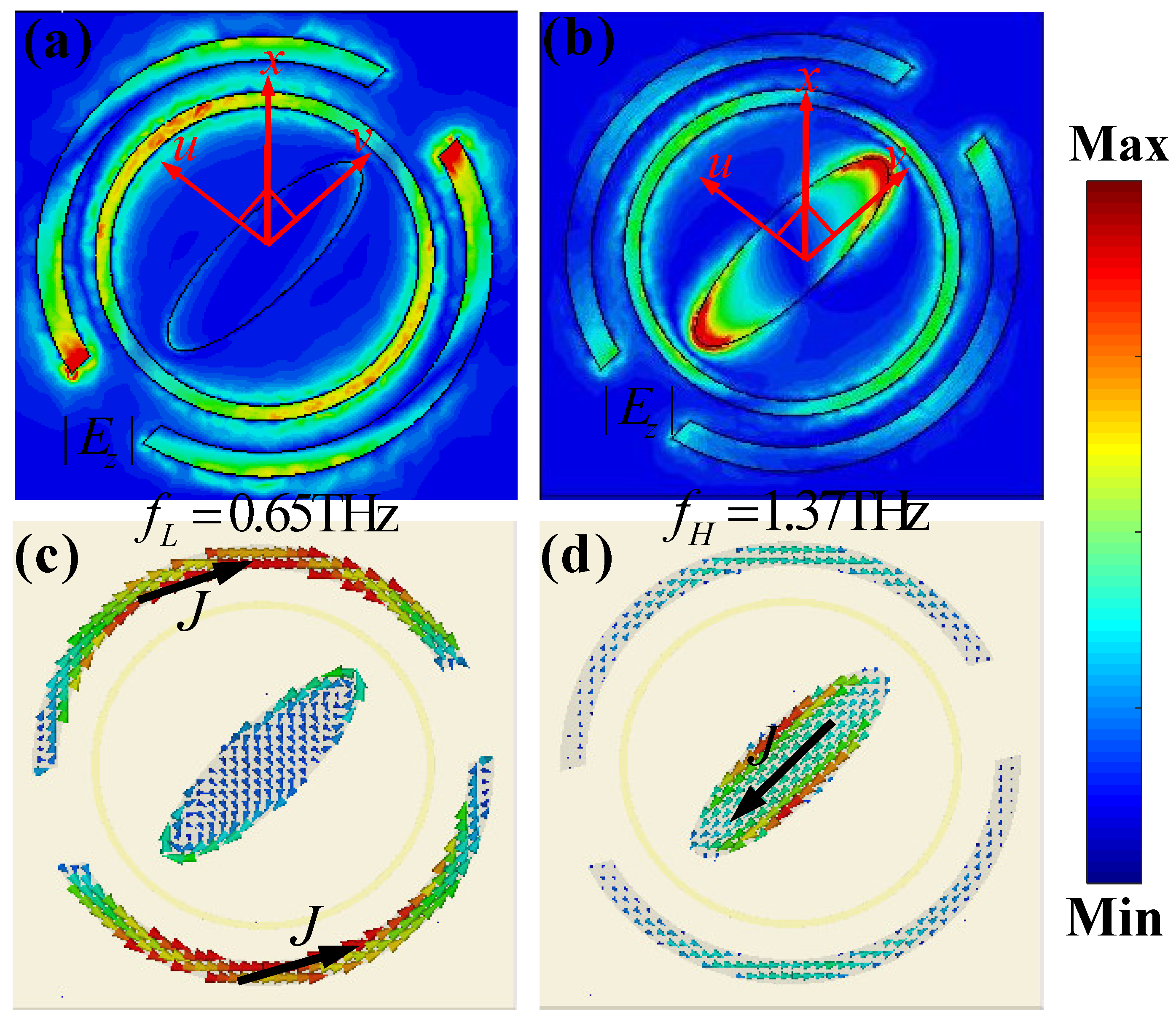
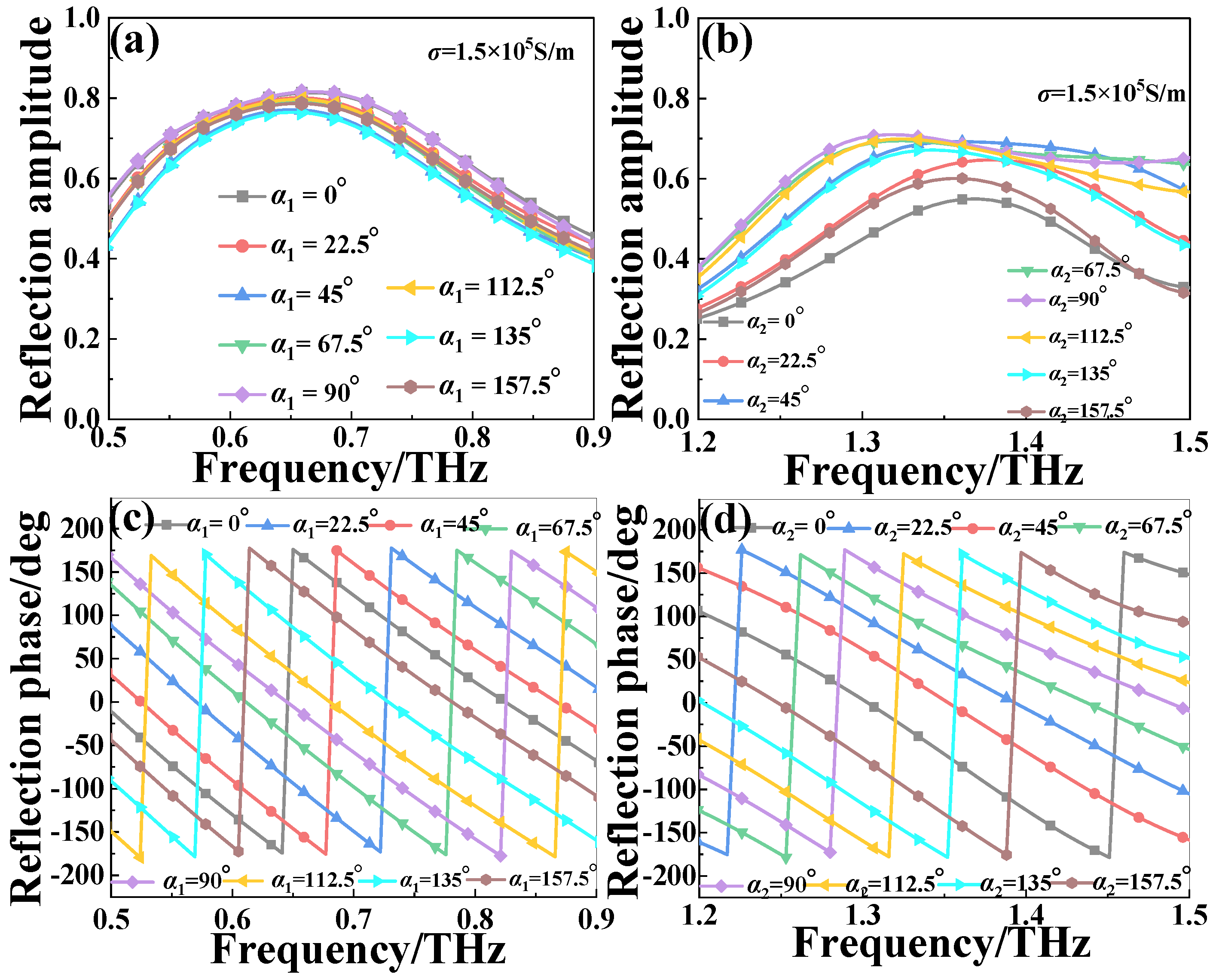
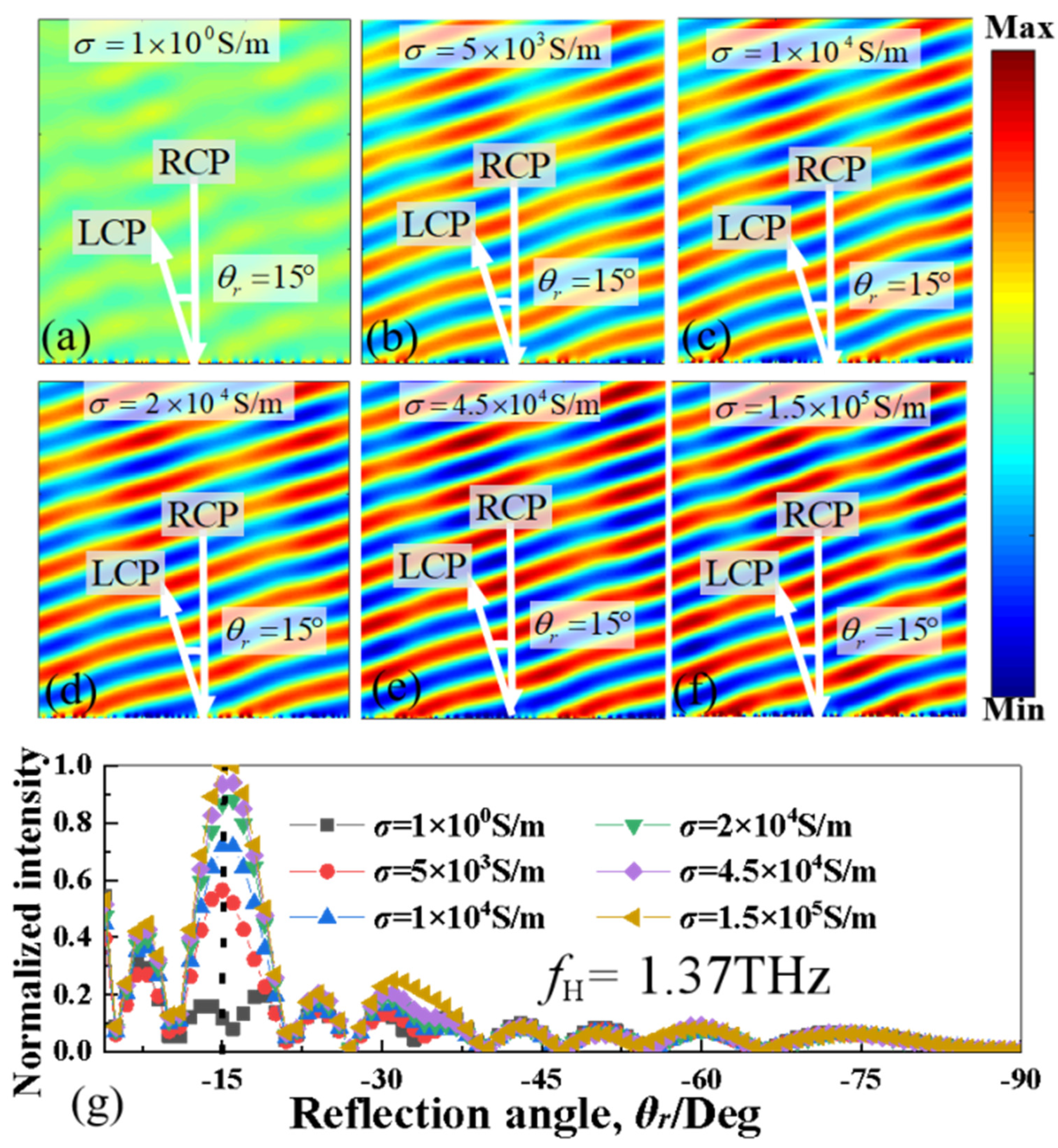
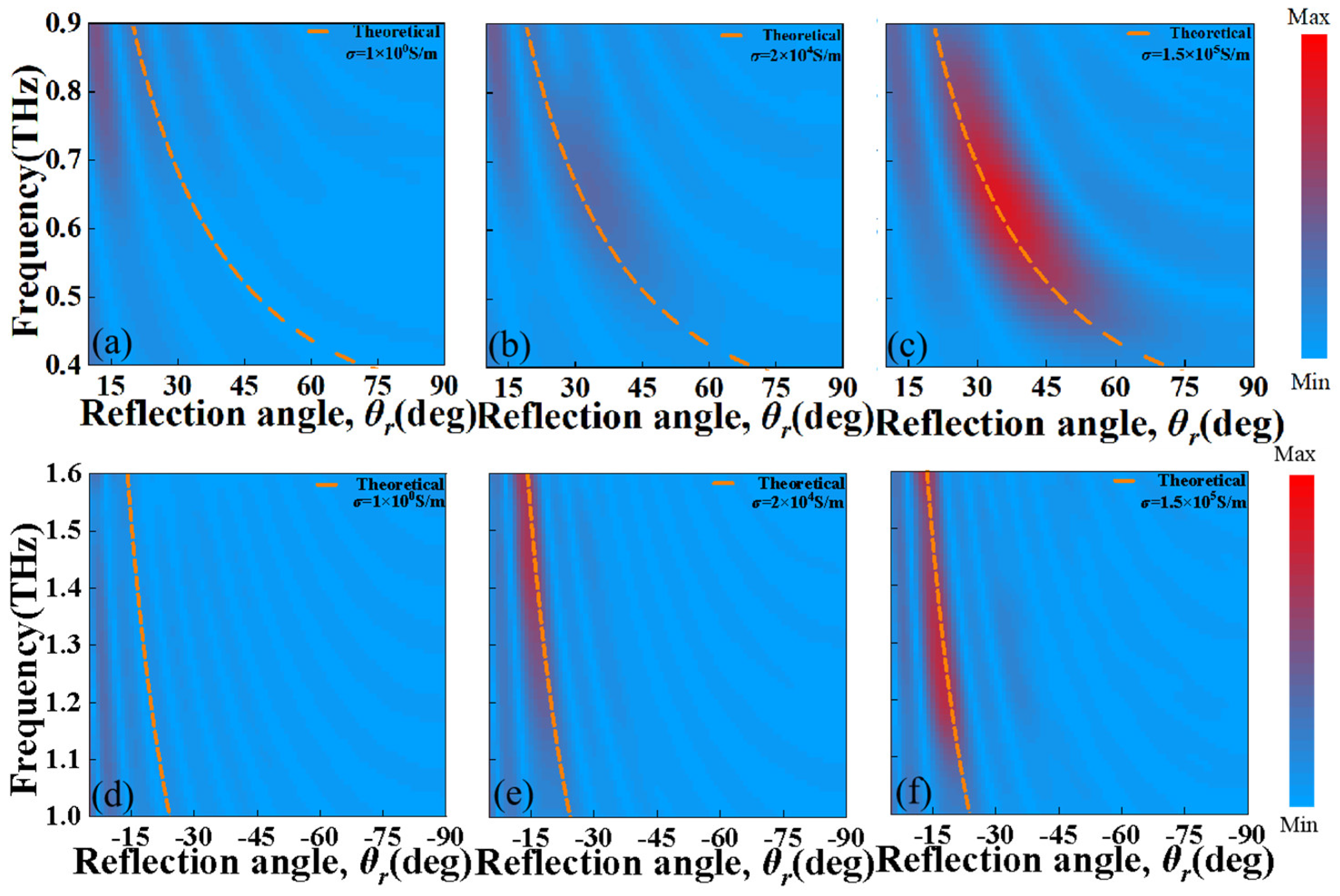
3. Results and Discussion

Figure 2 presents the reflection amplitude and polarization conversion ratio (PCR) for the structure under different infrared pump powers (the corresponding conductivity of photoconductive Si is from σsi = 1 S/m to σsi = 1.5 × 10⁵ S/m) at the lower and higher frequency ranges. Clearly when increasing the conductivity of photoconductive Si from 1 S/m to 1.5 × 10⁵ S/m, the amplitude and PCR of the reflected orthogonal CP wave for the normal incident RCP(LCP) wave will increase continuously at 0.4–0.9 THz and 1.2–1.5 THz, respectively. Here, we define the polarization conversion capability of the device as PCR:
{ PCR + = | r + | 2 | r + | 2 + | r + + | 2 PCR = | r + | 2 | r + | 2 + | r | 2
where the first subscript indicates the polarization state of the reflected wave, and the second subscript indicates the polarization state of the incident wave. For example, r−+ and r+− represent the orthogonal CP reflection coefficients, and the r++ and r−− denote the copolarization CP reflection coefficients.
As shown in Figure 2a,b, when σsi = 1 S/m, the reflection amplitude of the orthogonal CP wave for the proposed MS structure is only about 0.02 and 0.03 on average, and the corresponding PCR is near zero across the whole lower (0.4–0.9 THz) and higher (1.2–1.5 THz) frequency ranges (see Figure 2c,d). It reveals that nearly no reflective CP conversion occurs without infrared beam illumination, and the designed structure is in an “OFF” state in this case. In the absence of infrared beam illumination (σsi = 1 S/m), the outer CDSR and inner ESP photoconductive Si are in an isolation state, which can not effectively respond to the incident CP wave. When the structure is under the upper infrared pumping power (σsi = 1.5 × 10⁵ S/m), the reflection amplitude is up to the maximal values of 0.816 and 0.709, and the PCR is up to 96.6% and 89.3% at 0.65 THz and 1.37 THz, respectively, revealing the “ON” state in this case. It means that the reflective CP conversion efficiency from 0 to 96.6% and 0 to 89.3% can be adjusted dynamically through varying the external infrared pumping power of the designed MS at the above two distinct frequencies, respectively. To further illustrate the tunability of the proposed MS structure for the CP conversion, the modulation depth of the CP conversion is defined as d = PCRmax − PCRmin, where the PCRmax and PCRmin are the CP conversion efficiency when the proposed MS structure is under the upper limiting infrared pumping power (σsi = 1.5 × 10⁵ S/m) and without infrared pumping power (σsi = 1 S/m). Thus, the corresponding modulation depth of the CP conversion of the proposed structure is near 96.6% and 89.3% at the lower and higher frequencies, respectively. Therefore, the reflective CP conversion efficiency of the proposed MS can be tuned actively by changing the conductivity of the photoconductive Si through changing the infrared pumping power at two independent frequency ranges.
To illustrate the physics mechanism of the proposed MS for the CP conversion at two independent frequencies, we presented the induced z-component of the electric field (|Ez|) and surface current distributions on the unit-cell structure for the normal incident LCP wave under the upper infrared pumping power (σsi = 1.5 × 10⁵ S/m) at 0.65 THz and 1.37 THz, respectively.
Since both the outer CDSR and inner ESP structures are assumed as the evolved metal cut-wire structure resonators, thus, a similar electric response can be observed at the two distinct frequencies. As shown in Figure 3a,b, the induced z-component of the electric field (|Ez|) is mainly focused and distributed on the outer Si CDSR structure at the 0.65 THz, while the one is on the inner Si ESP structure at 1.37 THz. It means that the outer CDSR structure corresponds to the resonance response of the lower frequency, while the inner ESP structure to the one of the higher frequency. The electric fields of both the incident and the reflected CP waves are decomposed into two orthogonal components, i.e., u-component and v-component, respectively. The eigenmode resonances on the Si ESP and CDSR structures can be excited with electric components along the u- and v-axis directions, respectively. The excited dipole of the Si ESP and CDSR partly couples to the dipole mode on the interface of the top layer and air, leading to cross-polarization conversion after reflection. Obviously, the |Ez| distributions on the Si ESP and CDSR structures reveal effective excitation of the surface plasmon polaritons (SPPs) at resonances. As shown in Figure 3c,d, at the lower frequency of 0.65 THz, the induced surface current is mainly distributed on the upper and down edges of the outer CDSR structure, while the one is on the left-up and right-down edges of the part inner ESP structure at the higher frequency of 1.37 THz, which are both consistent well with the induced electric-field distributions along the v-axis direction, revealing strong electric dipolar resonance responses of the unit-cell structure for the normal incident LCP wave. Note that nearly no surface current distributions can be observed on the middle metal CR structure at the above two distinct frequencies. These electric-field and surface-current distributions on the unit cell reveal that the reflective CP conversion of the designed structure mainly originates from the fundamental dipolar resonance and structure anisotropy, showing that the respective control at two independent frequency regions is available.
To achieve the efficient reflective beam deflection effect for the CP wave, the full 2π phase coverage should be satisfied at the two distinct frequency ranges by rotating the αi (i = 1, 2) based on the PB phase principle instead of changing the structure parameter of the MS. Figure 4 presents the reflection amplitude and phase of the orthogonal CP wave of the proposed structure with different rotation angles (α1 and α2) under the upper infrared pump power (σsi = 1.5 × 10⁵ S/m). As shown in Figure 4a,c, at the lower frequency range of 0.5–0.9 THz, the designed MS exhibits a linear gradient phase of the reflected orthogonal CP wave when rotating the α1 of the outer CDSR structure by a step of 22.5° from 0° to 157.5°, while the corresponding amplitude is nearly unchanged. As shown in Figure 4b,d, at the higher frequency range of 1.2–1.5 THz, similar results for the reflection amplitude and phase also can be obtained by rotating the α2 of the inner ESP structure by a step of 22.5° from 0° to 157.5°. Obviously, the reflection amplitude of the orthogonal CP wave through the MS is very high and the corresponding phase is varied linearly with a certain interval by changing the α1 and α2. It means that the orthogonal reflection phase can realize the full coverage from 0 to 2π by respectively changing the α1 and α2 from 0° to 180° at the two independent frequency regions.
In the flowing section, we will study the THz beam deflection effect for the proposed MS based on the PB phase principle under infrared illumination with different pumping power. Here, as shown in Figure 5a, a supercell comprised of eight unit cells with different α1 and α2 has been designed to guarantee that the linear phase gradient from 0 to 2π with high efficiency can be achieved at two different frequency ranges. As shown in Figure 5b,c, when the designed supercell is illuminated by the infrared with upper pumping power (σsi = 1.5 × 10⁵ S/m) at fL/fH = 0.65/1.37 THz, the rotating angles α1/α2 of eight unit cells are 0°/−0.9°, 45°/45°, 90°/90°, 135°/135°, 178°/179°, −134°/−136°, −89°/−89°, and −46°/−44°, respectively. Obviously, the designed MS supercell exhibits a discontinued phase shift with nearly a step of 45° at 0.65 THz and 1.37 THz, respectively. In addition, as illustrated in Figure 5b,c, all reflection amplitudes for the selected eight unit cells of the designed supercell are about 0.8 and 0.65 on average at 0.65 THz and 1.37 THz, respectively, which is favorable to achieve the highly efficient beam deflection effect. By introducing a linear phase gradient, it is expected that the designed MS supercell can realize a THz beam deflection effect with continuous tunable efficiency under different infrared pumping power.
Based on the generalized Snell’s law, the beam deflection effect can be illustrated through the following equation [9,10]:
n r sin θ r n i sin θ i = λ 2 π d Φ ( x ) d x
where the incident angle is denoted as θi, while the reflection angle is represented by θr. The refraction indices of the medium in the incidence and reflection spaces are denoted as ni and nr, respectively. The λ refers to the operation wavelength in free space, and dΦ(x)/dx along the x direction signifies the phase gradient along the designed supercell interface. Using Equation (2), it can be observed that the output direction of the THz wave primarily depends on the discontinuous gradient phase of the designed supercell. When dΦ(x)/dx equals zero, the designed supercell only generates normal reflection for the normal incident THz wave. For practical simulation, the designed supercell is assumed to be in free space (ni = nr = 1), and the source is the normal incident LCP wave (θi = 0). Thus, the reflection angle can be obtained by simplifying Equation (2) as follow:
θ r = sin 1 ( λ g 0 2 π p )
where g0 and p are the phase gradient along the x direction and the periodicity of the unit cell, respectively. The theoretical value of the reflective deflection angle can be calculated by easily employing the simplified form of the generalized Snell law from Equation (3).
To confirm the continuous tunability of the THz beam deflection, the MS supercell is arranged with periodic boundary conditions in both the x and y-axis directions during simulation. In our designed MS supercell, the g0 is 45°, denoting the gradient phase. According to Equation (3), the theoretically calculated reflective deflection angle is about 35.2° and −15.3° at 0.65 THz and 1.37 THz, respectively.
Figure 6 and Figure 7 present the deflected electric field (|E|) distributions and corresponding normalized intensity of the orthogonal CP wave of the proposed MS supercell with different conductivity of photoconductive Si (σsi = 1 S/m, 5 × 10³ S/m, 1 × 10⁴ S/m, 2 × 10⁴ S/m, 4.5 × 10⁴ S/m, 1.5 × 10⁵ S/m) at 0.65 THz and 1.37 THz, respectively. The electric conductivity of photoconductive Si can be adjusted easily by changing the infrared pumping illumination power [49,50,51,52,53]. It is evident that the spatial deflection of the electric field results in the same reflective deflection angle at the same frequency but the corresponding normalized intensity decreases gradually when the electric conductivity of photoconductive Si decreases. As shown in Figure 6a, at 0.65 THz, when the MS with photoconductive Si has electric conductivity σsi = 1 S/m without infrared pumping illumination, the very weak electric field is directly reflected along the vertical direction without deflection. This is because the photoconductive Si is in an isolation state in the case without infrared pumping illumination, and the whole MS functioned as a mirror reflector. As illustrated in Figure 6b–f, when σsi = 1 S/m, 5 × 10³ S/m, 1 × 10⁴ S/m, 2 × 10⁴ S/m, 4.5 × 10⁴ S/m and 1.5 × 10⁵ S/m, the photoconductive Si is gradually changed from the isolation to metal state, the reflective deflected electric field distributions will become more and more obvious, and the deflection angle is always kept at about 35°, very close to the theoretical predication value of 35.2°. As depicted in Figure 6g, the normalized intensity of the deflected orthogonal CP wave beam will gradually increase with the increase of the electric conductivity of photoconductive Si. When σsi = 1 S/m without infrared pumping illumination, the normalized intensity of the deflected beam is near zero, which is consistent well with the electric-field distribution. When σsi increases from 5 × 10³ S/m to 1.5 × 10⁵ S/m, the normalized intensity of the deflected beam is increased from 0.1 to 1. This means that the efficiency of the deflected beam is highly dependent on the variation of the infrared pumping illumination power.
As shown in Figure 7, the similar electric field (|E|) distributions and normalized intensity of the deflected orthogonal CP beam can also be observed at the higher frequency of 1.37 THz. As depicted in Figure 7a–f, when σsi is changed from 1 S/m to 1.5 × 10⁵ S/m, the strength of the reflective deflected electric-field distributions will increasingly intensify, while the deflection angle remains consistently around −15°, closely approximating the theoretical value of −15.2°. As shown in Figure 7g, with the increase of the electric conductivity of photoconductive Si, the normalized intensity of the deflected orthogonal CP wave beam will gradually increase too. When the σsi is raised from 1 S/m to 1.5 × 10⁵ S/m, the normalized intensity of the deflected beam rises from 0.1 to 1, also indicating a strong reliance of the intensity of the deflected beam on changes of infrared pumping illumination power at the higher frequency of 1.37 THz.
To further illustrate the tunable reflection deflection effect of the designed MS, as shown in Figure 8, we present the simulated and theoretically calculated (dash line) reflection amplitude of the deflected orthogonal CP wave beam as functions of frequency and deflection angles for the designed MS with photoconductive Si of σsi = 1 S/m, 2 × 10⁴ S/m and 1.5 × 10⁵ S/m at the lower and higher frequency regions, respectively. From Figure 8, it is seen that the ordinary reflection (θr = 0°) is practically zero at the lower and higher frequency regions of 0.4–0.9 THz and 1–1.6 THz, and only the deflection CP wave beams are reflected with wide angle ranges of 17°–71° and 13°–23°, respectively, according to the generalized Snell law. Note that the theoretical calculation frequency deflection angles are the same when the designed MS with the photoconductive Si has a different electric conductivity at the same frequency range. It is evident that the frequency-dependent reflection deflection angle calculated using Equation (3) aligns well with the simulation results. From Figure 8a–f, it further confirms that the strength of the reflective deflected electric field will increasingly intensify when the electric conductivity of the photoconductive Si increases at both lower and higher frequency regions.

4. Conclusions

In conclusion, we have numerically demonstrated a photo-excited MS based on the hybrid patterned photoconductive Si structures in the THz region, which can independently realize the tunable reflective CP conversion and beam-deflection effect at two different frequencies. Numerical simulations show that the reflective CP conversion for the lower frequency region is controlled by the CDSR structure photoconductive Si of the designed MS, while the one of the higher frequency region is determined by the ESP structure. The electric conductivity of the structurally photoconductive Si can be modulated by changing the external infrared-beam pumping power. When the structurally photoconductive Si is in a metal state, the designed MS can convert the incident CP wave into its orthogonal components at two independent frequency regions. By increasing the electric conductivity of the structural photoconductive Si, the designed MS can realize a reflective CP conversion efficiency from 0 to 96.6% at 0.65 THz, and from 0 to 89.3% at 1.37 THz, respectively, and the corresponding modulation depth is up to 96.6% and 89.3%, respectively. Furthermore, the 2π phase shift also can be achieved by respectively rotating the oriented angle (αi) of the ESP and CDSR at two independent frequency regions. Finally, an MS supercell is constructed by carefully arranging the ESP and CDSR structures to achieve a reflective deflection effect, and the efficiency is tuned continuously from 0 to 99% at the two independent frequencies. The proposed MS in this study has a remarkable photo-excited response, which indicates its promising potential for deployment in active functional THz wavefront devices, including modulators, switches, and deflectors.

Author Contributions

Y.C. conceived the idea and set up the model; Z.X. performed the calculations and composed the first draft of the manuscript; C.N. and L.D. refined the model, and provided helpful discussions; Y.C. and L.W. coordinated the work. All authors have contributed to writing the manuscript. All authors have read and agreed to the published version of the manuscript.

Funding

This research was funded by the innovation project for university students in Hubei Province (Grant No. S202210488038).

Data Availability Statement

Not applicable.

Conflicts of Interest

The authors declare no conflict of interest.

References

  1. Yao, J.Q.; Li, J.; Zhang, Y.T.; Ding, X.; Wu, L. Terahertz wave modulation technology: Harnessing the light of terahertz. Nat. Mag. 2023, 45, 1–16. [Google Scholar]
  2. Fan, S.; He, Y.; Ung, B.S.; Pickwell-MacPherson, E. The growth of biomedical terahertz research. J. Phys. D Appl. Phys. 2014, 47, 374009. [Google Scholar] [CrossRef]
  3. Oh, S.J.; Kim, S.-H.; Jeong, K.; Park, Y.; Huh, Y.M.; Son, J.H.; Suh, J.S. Measurement depth enhancement in terahertz imaging of biological tissues. Opt. Express 2013, 21, 21299–21305. [Google Scholar] [CrossRef] [PubMed]
  4. Arbab, M.H.; Winebrenner, D.P.; Dickey, T.C.; Chen, A.; Klein, M.B.; Mourad, P.D. Terahertz spectroscopy for the assessment of burn injuries in vivo. J. Biomed. Opt. 2013, 18, 077004. [Google Scholar] [CrossRef] [Green Version]
  5. Shi, S.C.; Paine, S.; Yao, Q.J.; Lin, Z.H.; Li, X.X.; Duan, W.Y.; Matsuo, H.; Zhang, Q.; Yang, J.; Ashley, M.C.B.; et al. Terahertz and far-infrared windows opened at Dome A in Antarctica. Nat. Astron. 2017, 1, 0001. [Google Scholar] [CrossRef] [Green Version]
  6. Rappaport, T.S.; Xing, Y.C.; Kanhere, O.; Ju, S.; Madanayake, A.; Mandal, S.; Alkhateeb, A.; Trichopoulos, G.C. Wireless communications and applications above 100 GHz: Opportunities and challenges for 6G and beyond. IEEE Access 2019, 7, 78729–78757. [Google Scholar] [CrossRef]
  7. Pinaud, M.; Humbert, G.; Engelbrecht, S.; Merlat, L.; Fischer, B.M.; Crunteanu, A. Terahertz Devices Using the Optical Activation of Gete Phase Change Materials: Toward Fully Reconfigurable Functionalities. ACS Photonics 2021, 8, 3272–3281. [Google Scholar] [CrossRef]
  8. Fu, X.J.; Yang, F.; Liu, C.X.; Wu, X.; Cui, T.J. Terahertz Beam Steering Technologies: From Phased Arrays to Field-Programmable Metasurfaces. Adv. Opt. Mater. 2020, 8, 1900628. [Google Scholar] [CrossRef]
  9. Koch, M. Terahertz Technology: A Land to Be Discovered. Opt. Photonics News 2007, 18, 20–25. [Google Scholar] [CrossRef]
  10. Pendry, J.B.; Holden, A.J.; Stewart, W.J.; Youngs, I. Extremely low frequency plasmons in metallic mesostructures. Phys. Rev. Lett. 1996, 76, 4773–4776. [Google Scholar] [CrossRef] [Green Version]
  11. Pendry, J.B.; Holden, A.J.; Robbins, D.J.; Stewart, W.J. Magnetism from conductors and enhanced nonlinear phenomena. IEEE Trans. Microw. Theory Tech. 1999, 47, 2075–2084. [Google Scholar] [CrossRef] [Green Version]
  12. Smith, D.R.; Padilla, W.J.; Vier, D.C.; Nemat-Nasser, S.C.; Schultz, S. Composite medium with simultaneously negative permeability and permittivity. Phys. Rev. Lett. 2000, 84, 4184–4187. [Google Scholar] [CrossRef] [Green Version]
  13. Soukoulis, C.M.; Wegener, M. Past achievements and future challenges in the development of three-dimensional photonic metamaterials. Nat. Photonics 2011, 5, 523–530. [Google Scholar] [CrossRef] [Green Version]
  14. Shalaev, V.M. Optica lnegative-index metamaterials. Nat. Photonics 2007, 1, 41–48. [Google Scholar] [CrossRef]
  15. Shelby, R.A.; Smith, D.R.; Nemat Nasser, S.C.; Schultz, S. Microwave transmission through a two-dimensional, isotropic, left-handed metamaterials. Appl. Phys. Lett. 2001, 78, 489–491. [Google Scholar] [CrossRef] [Green Version]
  16. Pendry, J.B. Negative refraction makes a perfect lens. Phys. Rev. Lett. 2000, 85, 3966–3969. [Google Scholar] [CrossRef]
  17. Fang, N.; Lee, H.; Sun, C.; Zhang, X. Sub-diffraction-limited optical imaging with a silver superlens. Science 2005, 308, 534–537. [Google Scholar] [CrossRef] [PubMed] [Green Version]
  18. Pendry, J.B. Controlling electromagnetic fields. Science 2006, 312, 1780–1782. [Google Scholar] [CrossRef] [PubMed] [Green Version]
  19. Landy, N.I.; Sajuyigbe, S.; Mock, J.J.; Smith, D.R.; Padilla, W.J. Perfect metamaterial absorber. Phys. Rev. Lett. 2008, 100, 207402. [Google Scholar] [CrossRef] [PubMed]
  20. Hao, J.M.; Yuan, Y.; Ran, L.X.; Jiang, T.; Kong, J.A.; Chan, C.T.; Zhou, L. Manipulating electromagnetic wave polarizations by anisotropic metamaterials. Phys. Rev. Lett. 2007, 99, 063908. [Google Scholar] [CrossRef] [PubMed] [Green Version]
  21. Sun, W.J.; He, Q.; Hao, J.M.; Zhou, L. A transparent metamaterial to manipulate electromagnetic wave polarizations. Opt. Lett. 2011, 36, 927–929. [Google Scholar] [CrossRef] [Green Version]
  22. Burckel, D.B.; Wendt, J.R.; Eyck, G.A.T.; Ginn, J.C.; Ellis, A.R.; Brener, I.; Sinclair, M.B. Micrometer-Scale Cubic Unit Cell 3D Metamaterial Layers. Adv. Mater. 2010, 22, 4916. [Google Scholar] [CrossRef]
  23. Yu, N.F.; Genevet, P.; Kats, M.A.; Aieta, F.; Tetienne, J.P.; Capasso, F.; Gaburro, Z. Light Propagation with Phase Discontinuities Reflection and Refraction. Science 2011, 334, 333–337. [Google Scholar] [CrossRef] [PubMed] [Green Version]
  24. Glybovski, S.B.; Tretyakov, S.A.; Belov, P.A.; Kivshar, Y.S.; Simovski, C.R. Metasurfaces: From microwaves to visible. Phys. Rep. 2016, 634, 1–72. [Google Scholar] [CrossRef]
  25. Paul, O.; Reinhard, B.; Krolla, B.; Beigang, R.; Rahm, M. Gradient index metamaterial based on slot elements. Appl. Phys. Lett. 2010, 96, 241110. [Google Scholar] [CrossRef] [Green Version]
  26. Yang, D.R.; Cheng, Y.Z.; Chen, F.; Luo, H.; Wu, L. Efficiency tunable broadband terahertz graphene metasurface for circular polarization anomalous reflection and plane focusing effect. Diam. Relat. Mater. 2023, 131, 109605. [Google Scholar] [CrossRef]
  27. Cheng, Y.Z.; Qian, Y.J.; Luo, H.; Chen, F.; Cheng, Z.Z. Terahertz narrowband perfect metasurface absorber based on micro-ring-shaped GaAs array for enhanced refractive index sensing. Phys. E 2023, 146, 115527. [Google Scholar] [CrossRef]
  28. Li, Z.R.; Cheng, Y.Z.; Luo, H.; Chen, F.; Li, X.C. Dual-band tunable terahertz perfect absorber based on all-dielectric InSb resonator structure for sensing application. J. Alloys Compd. 2022, 925, 166617. [Google Scholar] [CrossRef]
  29. Zhu, X.Z.; Cheng, Y.Z.; Chen, F.; Luo, H.; Wu, L. Efficiency adjustable terahertz circular polarization anomalous refraction and planar focusing based on a bi-layered complementary Z-shaped graphene metasurface. Opt. Soc. Am. B 2022, 39, 705–712. [Google Scholar] [CrossRef]
  30. Chen, X.; Zou, H.; Su, M.; Tang, L.; Wang, C.; Chen, S.; Su, C.; Li, Y. All-Dielectric Metasurface-Based Beam Splitter with Arbitrary Splitting Ratio. Nanomaterials 2021, 11, 1137. [Google Scholar] [CrossRef]
  31. Fan, J.P.; Cheng, Y.Z.; He, B. High-Efficiency ultrathin terahertz geometric metasurface for full-space wavefront manipulation at two frequencies. Phys. D Appl. Phys. 2021, 54, 115101. [Google Scholar] [CrossRef]
  32. Li, J.; Cheng, Y.Z.; Li, X.C. Terahertz transmission-type metasurface for the linear and circular polarization wavefront manipulation. Adv. Theory Simul. 2022, 5, 127932. [Google Scholar] [CrossRef]
  33. Zhao, R.Q.; Zhu, Z.; Dong, G.H.; Lv, T.T.; Li, Y.X.; Guan, C.Y.; Shi, J.H.; Zhang, H. High-efficiency Huygens’ metasurface for terahertz wave manipulation. Opt. Lett. 2019, 44, 3482–3485. [Google Scholar] [CrossRef]
  34. Cheng, Y.Z.; Yu, J.W.; Li, X.C. Tri-band high-efficiency circular polarization convertor based on double-split-ring resonator structures. Appl. Phys. B 2022, 128, 1. [Google Scholar] [CrossRef]
  35. Liu, M.K.; Yang, Q.L.; Rifat, A.A.; Raj, V.; Komar, A.; Han, J.G.; Rahmani, M.; Hattori, T.H.; Neshev, D.; Powell, D.A.; et al. Deeply Subwavelength Metasurface Resonators for Terahertz Wavefront Manipulation. Adv. Opt. Mater. 2019, 7, 1900736. [Google Scholar] [CrossRef]
  36. You, X.; Fumeaux, C.; Withayachumnankul, W. Tutorial on broadband transmissive metasurfaces for wavefront and polarization control of terahertz waves. J. Appl. Phys. 2022, 131, 061101. [Google Scholar] [CrossRef]
  37. Jia, R.D.; Gao, Y.F.; Xu, Q.; Feng, X.; Wang, Q.W.; Gu, J.Q.; Tian, Z.; Ouyang, C.; Han, J.G.; Zhang, W.L. Achromatic Dielectric Metasurface with Linear Phase Gradient in the Terahertz Domain. Adv. Opt. Mater. 2021, 9, 2001403. [Google Scholar] [CrossRef]
  38. You, X.; Ako, R.T.; Lees, W.S.-L.; Bhaskaran, M.; Sriram, S.; Fumeaux, C.; Withayachumnankul, W. Terahertz transmissive half-wave metasurface with enhanced bandwidth. Opt. Lett. 2021, 46, 4164–4167. [Google Scholar] [CrossRef] [PubMed]
  39. Kan, T.; Isozaki, A.; Kanda, N.; Nemoto, N.; Konishi, K.; Takahashi, H.; Kuwata-Gonokami, M.; Matsumoto, K.; Shimoyama, I. Enantiomeric switching of chiral metamaterial for terahertz polarization modulation employing vertically deformable MEMS spirals. Nat. Commun. 2015, 6, 8422. [Google Scholar] [CrossRef] [PubMed] [Green Version]
  40. Konishi, K.; Kan, T.; Kuwata-Gonokami, M. Tunable and nonlinear metamaterials for controlling circular polarization. J. Appl. Phys. 2020, 127, 230902. [Google Scholar] [CrossRef]
  41. You, X.; Ako, R.T.; Bhaskaran, M.; Sriram, S.; Fumeaux, C.; Withayachumnankul, W. Mechanically tunable terahertz circular polarizer with versatile functions. Laser Photonics Rev. 2023, 17, 22000305. [Google Scholar] [CrossRef]
  42. Wu, T.S.; Liu, Z.H.; Wang, Y.P.; Zhang, H.X.; Yang, Z.N.; Cao, W.P.; Yang, D. All-Dielectric Phase-Gradient Metasurface Performing High-Efciency Anomalous Transmission in the Near-Infrared Region. Nanoscale Res. Lett. 2021, 16, 158. [Google Scholar] [CrossRef]
  43. Cheng, Y.Z.; Yang, D.R.; Li, X.C. Broadband reflective dual-functional polarization convertor based on all-metal metasurface in visible region. Phys. B Condens. Matter 2022, 640, 414047. [Google Scholar] [CrossRef]
  44. Shanei, M.M.; Fathi, D.; Ghasemifard, F.; Quevedo-Teruel, O. All-silicon reconfigurable metasurfaces for multifunction and tunable performance at optical frequencies based on glide symmetry. Sci. Rep. 2019, 9, 13641. [Google Scholar] [CrossRef] [PubMed] [Green Version]
  45. Su, X.Q.; Ouyang, C.; Xu, N.; Cao, W.; Wei, X.; Song, G.; Gu, J.; Tian, Z.; O’Hara, J.F.; Han, J.; et al. Active metasurface terahertz deflector with phase discontinuities. Opt. Express 2015, 23, 27152–27158. [Google Scholar] [CrossRef] [PubMed]
  46. Ha, Y.L.; Guo, Y.H.; Pu, M.B.; Li, X.; Ma, X.L.; Luo, X.G. A tunable metasurface deflector based on MIM waveguide Filled with Phase-Change Material. Plasmonics 2019, 14, 1735–1741. [Google Scholar] [CrossRef]
  47. Kim, S. Broadband phase-change metagrating design for efficient active reflection steering. Curr. Opt. Photonics 2021, 5, 134–140. [Google Scholar]
  48. Yu, F.L.; Zhao, Z.Y.; Chen, J.; Wang, J.; Jin, R.; Chen, J.; Wang, J.; Li, G.; Chen, X.; Lu, W. Reconfigurable metasurface with tunable and achromatic beam deflections. Opt. Mater. Express 2021, 12, 49–58. [Google Scholar] [CrossRef]
  49. Seren, H.R.; Keiser, G.R.; Cao, L.; Zhang, J.; Strikwerda, A.C.; Fan, K.; Metcalfe, G.D.; Wraback, M.; Zhang, X.; Averitt, R.D. Optically modulated multiband terahertz perfect absorber. Adv. Opt. Mater. 2014, 2, 1221–1226. [Google Scholar] [CrossRef]
  50. Cheng, Y.Z.; Gong, R.Z.; Zhao, J.C. A photoexcited switchable perfect metamaterial absorber/reflector with polarization-independent and wide-angle for terahertz waves. Opt. Mater. 2016, 62, 28–33. [Google Scholar] [CrossRef]
  51. Liu, X.W.; Liu, H.J.; Sun, Q.B.; Huang, N. Metamaterial terahertz switch based on split-ring resonator embedded with photoconductive Silicon. Appl. Opt. 2015, 54, 3478–3483. [Google Scholar] [CrossRef]
  52. Bing, P.B.; Guo, X.Y.; Wang, H.; Li, Z.Y.; Yao, J.Q. Characteristic analysis of a photoexcited tunable metamaterial absorber for terahertz waves. J. Opt. 2019, 48, 179–183. [Google Scholar] [CrossRef]
  53. Zhao, J.C.; Cheng, Y.Z.; Cheng, Z.Z. Design of a photo-excited switchable broadband reflective linear polarization conversion metasurface for terahertz waves. IEEE Photonics J. 2018, 10, 4600210. [Google Scholar] [CrossRef]
  54. Song, Z.Y.; Wang, Z.S.; Wei, M.L. Broadband tunable absorber for terahertz waves based on isotropic silicon metasurfaces. Mater. Lett. 2019, 234, 138–141. [Google Scholar] [CrossRef]
  55. Zhao, X.G.; Wang, Y.; Schalch, J.; Duan, G.W.; Cremin, K.; Zhang, J.D.; Chen, C.X.; Averitt, R.D.; Zhang, X. Optically Modulated Ultra-Broadband All Silicon Metamaterial Terahertz Absorbers. ACS Photonics 2019, 6, 830–837. [Google Scholar] [CrossRef]
  56. Wang, Y.; Yue, L.S.; Cui, Z.J.; Zhang, X.J.; Zhang, X.; Zhu, Y.Q.; Zhang, K. Optically tunable single narrow band all-dielectric terahertz metamaterials absorber. AIP Adv. 2020, 10, 045039. [Google Scholar] [CrossRef]
  57. Cheng, Y.Z.; Liu, J.Q.; Chen, F.; Luo, H.; Li, X.C. Optically switchable broadband metasurface absorber based on square ring shaped photoconductive silicon for terahertz waves. Phys. Lett. A 2021, 402, 127345. [Google Scholar] [CrossRef]
  58. Kanda, N.; Konishi, K.; Kuwata-Gonokami, M. All-photoinduced terahertz optical activity. Opt. Lett. 2014, 39, 3274–3277. [Google Scholar] [CrossRef]
  59. Kanda, N.; Konishi, K.; Kuwata-Gonokami, M. Dynamics of photo-induced terahertz optical activity in metal chiral gratings. Opt. Lett. 2012, 37, 3510–3512. [Google Scholar] [CrossRef]
  60. Li, N.; Zhao, J.; Tang, P.; Cheng, Y. Design of all-metal 3D anisotropic metamaterial for ultrabroadband terahertz reflective linear polarization conversion. Phys. Status Solidi B 2023, 5, 2300104. [Google Scholar] [CrossRef]
  61. Zhao, J.; Li, N.; Cheng, Y. All-dielectric InSb metasurface for broadband and high-efficient thermal tunable terahertz reflective linear-polarization conversion. Opt. Commun. 2023, 536, 129372. [Google Scholar]
  62. Li, N.; Zhao, J.; Tang, P.; Cheng, Y. Broadband and high-efficient reflective linear-circular polarization convertor based on three-dimensional all-metal anisotropic metamaterial at terahertz frequencies. Opt. Commun. 2023, 538, 129544. [Google Scholar] [CrossRef]
  63. Yang, D.R.; Cheng, Y.Z.; Luo, H.; Chen, F.; Wu, L. Ultra-thin and ultra-broadband terahertz single-layer metasurface based on double-arrow-shaped resonator structure for full-space wavefront manipulation. Adv. Theory Simul. 2023, 15, 312. [Google Scholar]
Figure 1. (a) Schemes of the proposed photo-excited MS: (a) periodic array, (b,c) front and perspective views of the unit cell.
Nanomaterials 13 01846 g001
Figure 2. The (a,b) reflection amplitude of the orthogonal CP wave and (c,d) the PCR at the (a,c) lower and (b,d) higher frequency regions for the proposed MS with different conductivity of photoconductive Si (from σsi = 1 S/m to σsi = 1.5 × 10⁵ S/m).
Nanomaterials 13 01846 g002
Figure 3. The distributions of the induced (a,b) electric fields (|Ez|) and (c,d) surface current of the proposed MS unit cell with photoconductive Si of conductivity σsi = 1.5 × 10⁵ S/m for the normal incident LCP wave at (a,c) 0.65 THz and (b,d) 1.37 THz.
Nanomaterials 13 01846 g003
Figure 4. The reflection (a,b) amplitude and phase (c,d) of the orthogonal CP wave of the proposed MS structure with different rotation angles (α1 and α2) with photoconductive Si of conductivity σsi = 1.5 × 10⁵ S/m.
Nanomaterials 13 01846 g004
Figure 5. (a) The scheme of the designed MS for the tunable THz deflector, the reflection amplitude, and the phase of the orthogonal CP wave of the proposed structure with photoconductive Si of conductivity σsi = 1.5 × 10⁵ S/m at (b) fL = 0.65 THz and (c) fH = 1.37 THz.
Nanomaterials 13 01846 g005
Figure 6. (af) The deflected electric field (|E|) distributions and (g) normalized intensity of the deflected orthogonal CP beam for the proposed MS supercell with different conductivity of photoconductive Si (from σsi = 1 S/m to σsi = 1.5 × 10⁵ S/m) at the lower frequency of 0.65 THz.
Nanomaterials 13 01846 g006
Figure 7. (af) The electric field (|E|) distributions and (g) normalized intensity of the deflected orthogonal CP beam for the proposed MS supercell with different conductivity of photoconductive Si (from σsi = 1 S/m to σsi = 1.5 × 10⁵ S/m) at the higher frequency of 1.37 THz.
Nanomaterials 13 01846 g007
Figure 8. The simulated and theoretical calculated (dash line) reflection amplitude of the deflected orthogonal CP beam as functions of frequency and deflection angles for the designed MS with photoconductive Si of (a,d) σsi= 1 S/m, (b,e) σsi = 2 × 10⁴ S/m and (c,f) σsi = 1.5 × 10⁵ S/m at (ac) the lower and (df) the higher frequency regions.
Nanomaterials 13 01846 g008
Disclaimer/Publisher’s Note: The statements, opinions and data contained in all publications are solely those of the individual author(s) and contributor(s) and not of MDPI and/or the editor(s). MDPI and/or the editor(s) disclaim responsibility for any injury to people or property resulting from any ideas, methods, instructions or products referred to in the content.

