Article

Carrier Modulation via Tunnel Oxide Passivating at Buried Perovskite Interface for Stable Carbon-Based Solar Cells

1
School of Automation, Zhongkai University of Agriculture and Engineering, Guangzhou 510225, China
2
Key Laboratory of Artificial Micro & Nano Structures of Ministry of Education, School of Physics and Technology, Wuhan University, Wuhan 430072, China
3
Key Laboratory of Advanced Optical Manufacturing Technologies of Jiangsu Province & Key Laboratory of Modern Optical Technologies of Education Ministry of China, School of Optoelectronic Science and Engineering & Collaborative Innovation Center of Suzhou Nano Science and Technology, Soochow University, Suzhou 215006, China
4
Department of Physics, School of Pure Sciences, College of Engineering Science and Technology, FIJI National University, Lautoka Campus, Suva 744101, Fiji
*
Authors to whom correspondence should be addressed.
Nanomaterials 2023, 13(19), 2640; https://doi.org/10.3390/nano13192640
Submission received: 4 September 2023 / Revised: 19 September 2023 / Accepted: 21 September 2023 / Published: 26 September 2023

Abstract

:
Carbon-based perovskite solar cells (C-PSCs) have the impressive characteristics of good stability and potential commercialization. The insulating layers play crucial roles in charge modulation at the buried perovskite interface in mesoporous C-PSCs. In this work, the effects of three different tunnel oxide layers on the performance of air-processed C-PSCs are scrutinized to unveil the passivating quality. Devices with ZrO2-passivated TiO2 electron contacts exhibit higher power conversion efficiencies (PCEs) than their Al2O3 and SiO2 counterparts. The porous feature and robust chemical properties of ZrO2 ensure the high quality of the perovskite absorber, thus ensuring the high repeatability of our devices. An efficiency level of 14.96% puts our device among the state-of-the-art hole-conductor-free C-PSCs, and our unencapsulated device maintains 88.9% of its initial performance after 11,520 h (480 days) of ambient storage. These results demonstrate that the function of tunnel oxides at the perovskite/electron contact interface is important to manipulate the charge transfer dynamics that critically affect the performance and stability of C-PSCs.

1. Introduction

Organic lead halide perovskite solar cells (PSCs) have emerged as a competitor of silicon photovoltaics regarding their high performance and commercial prospects. During the last few years, the power conversion efficiency (PCE) of PSCs improved from 3.8% to a recently certified 26.1% [1,2] as a result of relying on perovskite films with impressive properties, such as a high absorption coefficient, excellent ambipolar charge transport [3,4,5], long carrier diffusion lengths and a tunable bandgap [6,7,8,9,10]. Noble metals and organic hole-transporting materials (HTMs) are being widely employed for the preparation of state-of-the-art PSCs. However, their presence leads to an expensive manufacturing process and poor stability [11,12,13,14]. These issues could be overcome by the application of carbon counter electrodes (CEs) in hole-conductor-free PSCs. However, the removal of hole collection layers would sacrifice cell efficiency [15,16,17,18,19]. Currently, the PCE of hole-conductor-free C-PSCs is still lower than 20%, considerably lagging behind regular PSCs with fully functional layers [20,21].
Electron-collecting contacts play vital roles in determining the performance of common PSCs [22,23,24,25,26,27], especially that of carbon-based hole-transporting-layer-free PSCs (C-PSCs) [28,29,30]. Electron contacts simultaneously affect the charge transfer dynamics and influence the growth kinetics of the perovskite absorber [31]. Despite the fast progress and superior stability of C-PSCs [32], more in-depth research efforts are still required to improve the performance of C-PSCs. Since there are no HTMs in C-PSCs, charge manipulation and film growth modulation are more important than PSCs with fully functional layers [33]. Spike energy strategies that reduce the interface recombination are highly desired in inorganic photovoltaics [34,35]. SiO2 and Al2O3 have been introduced in silicon photovoltaics as electron tunneling paths forming the tunnel oxide passivated contacts on solar cells [36]. Similarly, insulating layers acting as energy band uplifters at the perovskite/TiO2 electron transport layer (ETL) interface are usually employed in mesoscopic PSCs [37,38,39]. Han and coworkers reported that modifying the ETL surface with an insulating material reduces the charge recombination and improves the open-circuit voltage (Voc) of the device PSCs [37]. Xu and coworkers found that introducing a thick (about 100 nanometers) Al2O3 insulator layer can reduce nonradiative recombination in PSCs [40]. Kamat and coworkers reported that hole accumulation can indirectly promote halide ion segregation in HTM-free PSCs with TiO2 ETLs, while insulating ZrO2 substrates suppresses phase segregation due to a more balanced charge transport [41].
In addition, the surface morphology of the underneath scaffold has a strong impact on the perovskite layer, which is paramount in influencing the final efficiency of PSCs. Zhu and coworkers investigated the compositional and optoelectronic properties of the buried perovskite interface [42]; they found that the bottom surfaces of perovskite films have severe compositional inhomogeneity and sub-microscale imperfections, causing major energy loss pathways that hinder device performance. They suggest that the underneath scaffolds play vital roles in the elimination of detrimental defects on the perovskite bottom surfaces. Therefore, surface topography tailoring should also be significantly considered in the optimization of C-PSCs. Regarding the charge transfer dynamics and perovskite film crystallization kinetics, the application criteria of Al2O3 [37], ZrO2 [18,38] and SiO2 [39] should be unveiled urgently.
In this work, we investigated the influence of tunnel oxide passivating (TOP) layers on the perovskite film quality and charge transporting properties of mesoscopic C-PSCs. TOP layers have several advantages in C-PSCs: first, they uplift the band bending at perovskite/ETL interfaces through the passivation of TiO2 surfaces by forming a discontinuous coating; second, they reduce charge shunting risks in the case of the presence of pinholes in the perovskite film; and, third, they modify the ETL with a porous topology more favorable for the solution infiltration of the perovskite precursor, leading to a higher absorber film quality and better interconnection with ETL networks. We selected commonly employed dielectric materials as tunnel oxides in PSCs, including Al2O3, SiO2 and ZrO2. In particular, ZrO2 has a relatively higher dielectric constant than TiO2, which might cause sufficient passivation on the TiO2 surface. Moreover, ZrO2 nanoparticle-coated scaffolds maintain high uniformity and porous features, facilitating perovskite crystallization and charge collection. An electrical impedance spectroscopy demonstrated that ZrO2 TOP-based C-PSCs show the best charge transfer properties with the highest efficiency of 14.96%. The efficient passivation with the tunnel oxide layer enables the high repeatability of our devices. Our HTM-free C-PSCs were fabricated under ambient conditions with a humidity of about 50%, further emphasizing the robust air stability that is compatible with high-yield manufacturing processes. Our C-PSCs present excellent long-term stability; they maintained 88.9% of their original efficiency after 11,520 h (480 days) of ambient storage without encapsulation.

2. Materials and Methods

2.1. Materials

Lead iodide (PbI2, 99.99%), CH3NH3I (MAI), bis(2,4-pentanedionato)-bis(2-propanolato)titanium(IV) (C16H28O6Ti) (75wt% in isopropanol) were purchased from TCI, isopropanol (IPA, 99.8%), diethanolamine (DMF, 99.8%), lead chloride (PbCl2, 99.99%), 1-butanol (99.8%), ZrO2 (50 nm, 99.99%), SiO2 (50 nm, 99.5%) and Al2O3 (γ phase, 20 nm, 99.99%)nanoparticles were obtained from Aladdin. The conductive carbon paste was synthesized according to our previous work [43].

2.2. Preparation of TiO2, ZrO2, Al2O3, SiO2 Paste

ZrO2, Al2O3 andSiO2 pastes were prepared by ball-milling 1.4 g powders of commercial ZrO2, Al2O3, SiO2, 0.7 g ethylcellulose, 5.77 g terpineol and 23.61 g ethanol for 24 h. The as-prepared ZrO2 and Al2O3 pastes were subsequently diluted with ethanol in ratios of 1, 2, 3 and 4 times by weight to obtain the optimal thickness of tunnel oxide layers. The high concentration of original pastes resulted in excessively thick insulating layers on the surface of the TiO2 electron transporting layer (ETL), thereby impeding charge transport and reducing the performance of C-PSCs. The TiO2 paste was prepared using a recipe that was similar to the published work [44].

2.3. Fabrication of C-PSCs

The process for fabricating C-PSCs involved several steps. First, the FTO glass was patterned by etching with Zn powder and 2 M HCl diluted in ethanol. The surface of the glass was then cleaned using acetone, deionized water, acetone and ethanol alternately, and dried in clean air. A solution of 0.15 M titanium diisopropoxidebis(acetylacetone) in 1-butanol was spin-coated on the cleaned FTO glass at 3000 rpm for 30 s, and dried at 125 °C for 20 min to form a compact TiO2 layer. The mesoporous TiO2 layer was deposited over the compact TiO2 layer by spin-coating a homemade TiO2 P25 paste at 3000 rpm for 20 s. The deposited layers were then sintered in air at 500 °C for 30 min. After cooling down to room temperature, the films were treated with a 0.05 M aqueous solution of TiCl4 at 70 °C for 30 min, rinsed with deionized water and ethanol, and dried in the air. Insulating layers were prepared by spin-coating ZrO2, Al2O3 or SiO2 paste over the TiCl4-treated TiO2 film and annealing it at 500 °C for 30 min. The perovskite film was deposited on the mesoporous TiO2 film using a two-step sequential method under ambient conditions with high humidity (~50%). In the first step, the PbI2 precursor solution was spin coated at 4000 rpm for 20 s and then the wet PbI2 film was treated with ethanol and annealed at 100 °C for 8 min. In the second step, the film was immersed in an isopropanol solution of MAI (7 mg mL−1) for 5 min and dried with nitrogen gas. The as-prepared MAPbI3 perovskite film was further heated at 100 °C for 10 min. Finally, the carbon paste was coated over the perovskite film using a doctor-blade method and annealed at 100 °C for 40 min. The resulting solar cells had a configuration of FTO/c-TiO2/meso-TiO2/TOP layer/MAPbI3/carbon.

2.4. Measurements and Characterization

The Bruker instrument (D8 Focus diffractometer) utilizing Cu Kα radiation (λ = 0.15406 nm) at 40 kV and 40 mA was employed for structural analysis. The surface and cross-sectional morphology were observed by a field emission scanning electron microscope (SEM, Zeiss SIGMA, Jena, Germany). The absorption spectra of films deposited on FTO were collected using a UV-vis spectrophotometer (Lambda 650S, PerkinElmer, Shelton, CT, USA) with a wavelength range of 300–800 nm at room temperature. The J-V curves of the solar cells were measured using a CHI660C electrochemical workstation (Shanghai, Chenhua) coupled with a solar simulator (Newport, 91192) under 100 mW cm−2 illumination (AM 1.5 G) with a scan rate of 0.05 V s−1. The area of the portion of C-PSC exposed to the radiation was confined to 0.1 cm2 using a metal mask. The films were characterized by ambient air condition, with a temperature of around 25 °C and relative humidity of 50%. The time-resolved photoluminescence (TRPL) was performed using a time-correlated single photon counting (TCSPC) module, excited with a 532 nm pulsed laser. The external quantum efficiency (EQE) was measured using an instrument equipped with a 300 W xenon lamp (Newport 66984), and the monochromatic light ranged from 300 to 800 nm. Electrochemical impedance spectra (EIS) were recorded under one sun illumination over the range of frequencies spanning from 1 MHz to 1 Hz at open-circuit voltage bias. During the long-term stability test, we stored the devices under room light without further protection. As aging progressed, the devices exhibited gradually increased performance for hundreds of hours before beginning to decline. The devices were exposed to room light during storage.

3. Results and Discussion

The C-PSCs possess a straightforward device architecture comprising FTO/TiO2/TOP layer/perovskite/carbon, as depicted in Figure 1a. Here, FTO refers to fluorine-doped tin oxide, and the perovskite layer corresponds to CH3NH3PbI3 (MAPbI3). The entire fabrication process was conducted in ambient air, with the perovskite layer deposited using a two-step sequential method, and the carbon electrode doctor-blade coated onto the perovskite film using the homemade carbon paste [43]. Our previous research indicates that high-temperature annealed TiO2 films exhibit numerous surface defects, which should be responsible for the inferior performance of C-PSCs [44]. We randomly used TiCl4 post-treatment and an external SiO2 coating to passivate the ETL surfaces, and the PCEs have been improved for the corresponding C-PSCs due to the elimination of interface defects [38,44]. However, the criteria for selecting surface passivating layers remain unclear. Drawing inspiration from the optimization processes of silicon (Si) solar cells, we deliberately selected SiO2, Al2O3 and ZrO2 as the TOP layers, taking into account their surface charge states, dialectical constants, film topologies and interface electric fields. Efficient C-PSCs require optimal TOP layers. Thus, we initially investigated the concentrations of SiO2, ZrO2 and Al2O3 pastes by diluting the original pastes with ethanol. Figure 1b shows the typical energy level diagram of the C-PSC that employs the ZrO2 TOP layer. The thin ZrO2 TOP layer exhibits a deep valence band maximum (VBM), with its conduction band position surpassing that of TiO2 [37]. Photo-generated electrons in the perovskite absorber layer may transfer from the conduction band (CB) of MAPbI3 to TiO2 through either the tunneling effect or the voids of the discontinued insulating layer coated on the thick mesoporous TiO2 scaffold. Consequently, electrons accumulate at the TiO2 interface due to the existence of this layer of insulating oxide, ultimately elevating the Fermi level and increasing the Voc of the solar cell. Simultaneously, due to the blocking effect of the insulating layers, it becomes challenging for electrons in the conduction band of TiO2 to recombine with holes. Therefore, a thin layer of insulating materials can reduce interfacial recombination, thereby facilitating carrier transport [40].
The variation in photovoltaic parameters of C-PSCs employing different concentrations of ZrO2 and Al2O3 pastes are shown in Figure 2a,b, respectively. As the concentration of ZrO2 or Al2O3 increases, the photovoltaic parameters, including Voc, Jsc, FF and PCE, first exhibit an increase and then a decrease trend. This can be ascribed to the thickness of the tunnel oxide layers, which is tuned by the concentration of the pastes. For the non-treated C-PSCs, severe charge recombination occurs at the buried perovskite interface due to the presence of defects, leading to inferior performance. However, if the concentration of ZrO2 or Al2O3 is too high, the thickness will be thick enough to suppress the electron transportation process, ultimately reducing the performance of final devices. The optimal weight ratio of ethanol to ZrO2 and Al2O3 pastes is found to be 1:1 and 2:1, respectively. The SiO2 TOP layer used here is the same as that reported in our previous work [38].
Figure 3a,b shows the cross-sectional SEM images of the full device and perovskite film grown on the TiO2/ZrO2 layer, respectively. The thicknesses of FTO, TiO2/ZrO2 and MAPbI3 are about 380 nm, 460 nm and 530 nm, respectively. The images reveal that the perovskite materials infiltrate well into the pores and the carbon electrode tightly adheres to the perovskite film.
The surface morphology and structure of scaffold layers play a crucial role in the performance of mesoscopic PSCs. Factors such as surface roughness, pore size and hydrophilicity have a significant impact on the infiltration of perovskite materials, crystallization quality and carrier transportation in the device [37]. Figure 4a–d shows the surface morphology of various scaffold layers (left column) and the perovskite grown on them (right column). TiO2 film shows a relatively uniform surface, with some nanoparticle agglomeration. In contrast, the TiO2/ZrO2 film exhibits a homogeneous morphology with well-dispersed top ZrO2 nanoparticles, which facilitates the infiltration and growth of perovskite materials, thereby promoting the transport of photo-generated carriers. However, the pores in the TiO2/Al2O3 scaffold are very small, which will hinder the infiltration of the precursor solution and limit the growth and crystallization of MAPbI3 in the pores. The TiO2/SiO2 film shows serious agglomeration, resulting in a rough surface with an exposed TiO2 layer that weakens the effect of the insulation layer as a separator between the carbon electrode and TiO2 layer, leading to a higher risk of shunting. All perovskite films grown on different scaffold layers show nanocube-like structures, indicating that the addition of insulating oxide has little effect on their surface morphology. Therefore, the improvement in PSCs’ performance is not only caused by the morphology of the perovskite but also by the modulation of the TOP layer on the carriers, which will be discussed later.
Figure 4e shows the XRD patterns of TiO2, TiO2/ZrO2, TiO2/Al2O3 and TiO2/SiO2 films. Except for the TiO2/ZrO2 film that shows a ZrO2 tetragonal phase at 2θ~29.2° [45], the XRD patterns for the rest of the films are identical to that of the TiO2 film without new peaks belonging to SiO2 or Al2O3. This means that the SiO2 or Al2O3 present in the TiO2 film is in the amorphous phase rather than the crystal phase, which could be attributed to the higher sintering temperatures required to form the phases [46,47]. The XRD patterns of perovskite films coated on different metal oxide films reveal similar features, indicating that the introduction of insulating layers does not affect the crystallization of perovskite inside. The diffraction peak observed at around 12.7° corresponds to PbI2, resulting from the presence of excess lead iodide in the perovskite, which can contribute to the increase in the Voc of PSCs [48].
In addition, we studied the UV-Vis absorption spectra for ETLs and MAPbI3 perovskite films grown over different insulating layers, as shown in Figure 5a,b, respectively. The absorption spectra of the scaffolds with various insulating layers exhibit negligible differences. The absorption of perovskite films is slightly increased after the addition of the insulating layers, which may be caused by the increased thickness of the scaffold layers resulting from the introduction of the insulating layers so that more perovskites can be loaded.
N2 adsorption–desorption isotherms were recorded for the powders of TiO2, ZrO2, Al2O3 and SiO2, as shown in Figure S1a–d. The inset shows the corresponding pore-size distribution curves obtained by the Barrett–Joyner–Halenda (BJH) method. The isotherms of the samples are the originated classic type IV isotherms of H3 hysteresis loop, indicating the existence of mesopores (2–50 nm) originating from the aggregated nanoparticles. This is consistent with the results observed from the SEM. The TiO2 and Al2O3 exhibit relatively narrower pore size distribution. The pore diameter of TiO2 ranges from 62 nm to 88 nm, while Al2O3 shows the smallest pore size of ~20 nm. The smaller pores may facilitate poor penetration of PbI2 into the TiO2 mesoporous scaffold and hinder the growth of perovskite. However, ZrO2 and SiO2 exhibit a wide range of pore-size distribution. The ZrO2 is mainly composed of macropores with a size of the order of 100–165 nm, and the pore size of SiO2 is distributed between 50 and 120 nm. Therefore, the relatively larger pore size corresponding to the ZrO2 can accommodate more perovskite in the scaffold layer, which, in turn, facilitates better light harvesting and higher electron collection efficiency.
We prepared a large number of C-PSCs to study the effects of different insulation layers on photovoltaic performance. Figure 6a–d shows the statistics of photovoltaic parameters, including Voc, short circuit current density (Jsc), FF and PCE, and the corresponding average values are summarized in Table 1. Each parameter was calculated from 40 devices. The C-PSC without an insulating layer shows an average Voc of 0.959 V, a Jsc of 20.29 mA cm−2 and an FF value of 65.25%, yielding an average PCE value of 12.71%. The average PCE values of C-PSCs that employ ZrO2, Al2O3 and SiO2 as insulation layers are increased to 13.84%, 12.89% and 13.42%, respectively. The increase in PCE is mainly due to the enhancement of Voc and FF, which can be attributed to the inhibition of carrier recombination by insulation layers, as discussed above. As mentioned previously, after TOP layer coating, the absorption of the perovskite film slightly increases. Therefore, more light energy can be collected and the Jsc of the solar cell is increased accordingly. The improvement in average PCE for PSCs employing ZrO2 as the insulating layer is noticeably higher than that of PSCs using Al2O3 and SiO2. This could be due to the uniform and porous morphology of ZrO2 promoting the effective permeation of PbI2 into the mesoporous TiO2 scaffold layer, thereby facilitating charge transport. As shown in Figure S2, our devices exhibit good reproducibility with a small deviation in PCE.
Figure 6e shows the J-V curves of the best-performing devices with different scaffold layers, with the corresponding photovoltaic parameters listed in the inset. The device with a ZrO2 insulating layer exhibits excellent performance, with a Voc of 0.995 V, a Jsc of 21.21 mA cm−2 and an FF of 70.91%, yielding a PCE of 14.96%. Figure 6f shows the incident photon-to-electron conversion efficiency (IPCE) spectrum of a C-PSC prepared on TiO2/ZrO2 film. The measured integral Jsc from the IPCE spectrum is also shown in Figure 6f. The resulting integrated Jsc value is 20.92 mA cm−2, which is only ~1.4% lower than that of the champion cell (21.21 mA cm−2) in Figure 6e.
The perovskite films deposited on the surface of the insulating layers, as shown in Figure 7a, have a stable PL intensity lower than that deposited on the TiO2 surface, suggesting that the introduction of the TOP layer increases the transport and extraction efficiency of the carrier. The strongest PL quenching occurred on the perovskite film deposited on TiO2/ZrO2, indicating that ZrO2 has better charge modulation capabilities. We further performed a time-resolved photoluminescence (TRPL) test of the perovskite films. The TRPL data are fitted by a biexponential decay model and the corresponding lifetime values are listed in the inset of Figure 7b. The average carrier lifetime of TiO2/perovskite film is 110.5 ns. After the introduction of the ZrO2 insulating layer for TiO2, the average carrier lifetime reduces to 82.5 ns, indicating improved charge transport. However, for the TiO2/Al2O3/perovskite and TiO2/SiO2/perovskite films, the carrier lifetime increases to 125.6 and 108.3 ns, respectively.
To further investigate the kinetics of charge transport and recombination in perovskite solar cells, we measured the electrical impedance spectroscopy (EIS). The Nyquist plots of our C-PSCs, employing different insulating layers, are shown in Figure 7c. The semicircles at high- and low-frequency regions can be assigned to the charge transport resistance (Rct) and recombination resistance (Rrec), respectively [43]. The corresponding impedance parameters are listed in Table 2. It is found that Rct slightly decreases with the addition of ZrO2 or SiO2, indicating that the presence of ZrO2 or SiO2 has a slight promoting effect on charge transport. However, after Al2O3 treatment, Rct increases from 44.5 to 50.4 Ω due to hindered charge transport by the addition of dense Al2O3. On the other hand, Rrec obviously increases with the incorporation of insulating layers, indicating effectively suppressed charge recombination, which confirms our previous expectation that insulating layers can prevent direct contact with carbon and TiO2 [38]. In general, ZrO2-based C-PSC has the smallest Rct and the largest Rrec, indicating faster carrier transport and slower recombination, which well explains the significant improvement in the Voc and FF of corresponding devices. The buried interface quality has been highly improved due to carrier modulation with highly suppressed nonradiative recombination.
To further confirm the reliability of our fabricated C-PSCs, the steady-state efficiency of C-PSC fabricated on TiO2/ZrO2 is measured in ambient air under a constant bias of 0.8 V near the maximum power point. As shown in Figure 8a, our device presents a stable current density of 17.55 mA cm−2 under continuous illumination for 400 s, and the corresponding PCE is 14.04%. In comparison, the original TiO2-based device produces only 12.83% steady-state PCE under the same test condition, with a current density of 16.04 mA cm−2 (Figure 8b).
Since the stability of PSC is one of the most critical concerns for the future commercialization of the devices, we have also recorded the stability of C-PSCs prepared on TiO2/ZrO2 to verify the long-term endurance in ambient air conditions with a temperature of 25 °C and humidity of 50 RH%. As shown in Figure 9, the Voc slightly increases during the stability test, while Jsc and FF first increase and then show a decreasing trend. The PCE increases from an initial 13.96% to the highest of 15.24%, and finally drops to 12.41% after being stored for 11,520 h (480 days), demonstrating the outstanding stability of C-PSCs, which is among the first class of state-of-the-art devices [18,32]. The better performance during storage may be ascribed to the better contact attained between the perovskite layer and the carbon CE [43]. We further investigated the thermal stability of our unencapsulated devices by placing them on a heating plate at 85 °C in an environment with a humidity of 50%. Figure S3 shows the variation in PCE with heating time. The PCE initially improved slightly; however, it reduced to 81% of the initial value after 120 h of continuous heating. This may be caused by the decomposition of perovskite material in unencapsulated devices triggered by the high-humidity environment.

4. Conclusions

In summary, ZrO2, Al2O3, and SiO2 are successfully used as insulating TOP layers for air-processed, highly efficient and stable C-PSCs. These common insulating materials can effectively separate TiO2 ETL and carbon electrodes, thus efficiently inhibiting carrier recombination caused by shunting. The main reason for the variation in improving the performance of C-PSCs lies in the morphology of insulating layers, which affects the infiltration and growth of perovskite material. We achieved the best performance of C-PSCs with a PCE of 14.96% using TiO2/ZrO2 as a scaffold layer, indicating that ZrO2 is the most suitable insulating layer for the system of C-PSCs. Moreover, our C-PSCs show outstanding long-term stability, maintaining 88.9% of their initial efficiency after 11,520 h storage in ambient air. This work is promising for high performance carbon-based HTM-free perovskite solar cells via the optimization of insulation materials. The high efficiency and stability in our TOP layer passivated C-PSCs offer a step towards the future commercialization of this low-cost photovoltaic technology.

Supplementary Materials

The following supporting information can be downloaded at: https://www.mdpi.com/article/10.3390/nano13192640/s1, Figure S1: The N2 adsorption–desorption isotherms and corresponding pore size distribution curves (inset) of (a) TiO2, (b) ZrO2, (c) Al2O3 and (d) SiO2; Figure S2: Histograms of solar cell efficiencies were collected from 40 cells with ZrO2 TOP; Figure S3: Environmental thermal stress (85 °C in a heating panel) with high humidity (40–60%) conditions.

Author Contributions

Conceptualization, Y.X. and C.W.; Formal analysis, Y.Z. and K.K.K.; Funding acquisition, Y.X. and C.W.; Investigation, Y.X. and H.Z.; Project administration, C.W.; Validation, H.Z. and P.L.; Writing—original draft, Y.X.; Writing—review and editing, K.K.K. and C.W. All authors have read and agreed to the published version of the manuscript.

Funding

This research was funded by the Science and Technology Program of Guangzhou (2023A04J2035), National Natural Science Foundation of China (No. 61974106, 11904132, 61975065 and 62005188), Natural Science Foundation of Jiangsu Province (BK20190825).

Data Availability Statement

Not applicable.

Conflicts of Interest

The authors declare no conflict of interest.

References

  1. Kojima, A.; Teshima, K.; Shirai, Y.; Miyasaka, T. Organometal halide perovskites as visible-light sensitizers for photovoltaic cells. J. Am. Chem. Soc. 2009, 131, 6050–6051. [Google Scholar] [CrossRef]
  2. Interactive Best Research-Cell Efficiency Chart. Available online: https://www.nrel.gov/pv/interactive-cell-efficiency.html (accessed on 25 July 2023).
  3. Lee, M.M.; Teuscher, J.; Miyasaka, T.; Murakami, T.N.; Snaith, H.J. Efficient hybrid solar cells based on meso-super structured organometal halide perovskites. Science 2012, 338, 643–647. [Google Scholar] [CrossRef]
  4. Innocenzo, V.D.; Grancini, G.; Alcocer, M.J.P.; Kandada, A.R.S.; Stranks, S.D.; Lee, M.M.; Lanzani, G.; Snaith, H.J.; Petrozza, A. Excitons versus free charges in organo-lead tri-halide perovskites. Nat. Commun. 2014, 5, 3586. [Google Scholar] [CrossRef]
  5. Zhu, J.W.; Luo, Y.; He, R.; Chen, C.; Wang, Y.; Luo, J.C.; Yi, Z.J.; Thiesbrummel, J.; Wang, C.L.; Lang, F.L.; et al. A donor-acceptor-type hole-selective contact reducing non-radiative recombination losses in both subcells towards efficient all-perovskite tandems. Nat. Energy 2023, 8, 714–724. [Google Scholar] [CrossRef]
  6. Xing, G.; Mathews, N.; Sun, S.; Lim, S.S.; Lam, Y.M.; Grätzel, M.; Mhaisalkar, S.; Sum, T.C. Long-range balanced electron- and hole-transport lengths in organic-inorganic CH3NH3PbI3. Science 2013, 342, 344–347. [Google Scholar] [CrossRef]
  7. Dong, Q.; Fang, Y.; Shao, Y.; Mulligan, P.; Qiu, J.; Cao, L.; Huang, J. Electron-hole diffusion lengths > 175 μm in solution-grown CH3NH3PbI3 single crystals. Science 2015, 347, 967–970. [Google Scholar] [CrossRef]
  8. Gharibzadeh, S.; Hossain, I.M.; Fassl, P.; Nejand, B.A.; Abzieher, T.; Schultes, M.; Ahlswede, E.; Jackson, P.; Powalla, M.; Schäfer, S.; et al. 2D/3D heterostructure for semitransparent perovskite solar cells with engineered bandgap enables efficiencies exceeding 25% in four-terminal tandems with silicon and CIGS. Adv. Funct. Mater. 2020, 30, 1909919. [Google Scholar] [CrossRef]
  9. Zhong, J.X.; Wu, W.Q.; Ding, L.; Kuang, D.B. Blade-coating perovskite films with diverse compositions for efficient photovoltaics. Energy Environ. Mater. 2021, 4, 277–283. [Google Scholar] [CrossRef]
  10. El-Ballouli, A.A.O.; Bakr, O.M.; Mohammed, O.F. Compositional, processing, and interfacial engineering of nanocrystal- and quantum-dot-based perovskite solar cells. Chem. Mater. 2019, 31, 6387–6411. [Google Scholar] [CrossRef]
  11. Sutanto, A.A.; Caprioglio, P.; Drigo, N.; Hofstetter, Y.J.; Garcia-Benito, I.; Queloz, V.I.E.; Neher, D.; Nazeeruddin, M.K.; Stolterfoht, M.; Vaynzof, Y.; et al. 2D/3D perovskite engineering eliminates interfacial recombination losses in hybrid perovskite solar cells. Chem 2021, 7, 1903–1916. [Google Scholar] [CrossRef]
  12. Park, N.; Zhu, K. Scalable fabrication and coating methods for perovskite solar cells and solar modules. Nat. Rev. Mater. 2020, 5, 333–350. [Google Scholar] [CrossRef]
  13. Jiang, Q.; Zhao, Y.; Zhang, X.; Yang, X.; Chen, Y.; Chu, Z.; Ye, Q.; Li, X.; Yin, Z.; You, J. Surface passivation of perovskite film for efficient solar cells. Nat. Photonics 2019, 13, 460–466. [Google Scholar] [CrossRef]
  14. Zhu, H.; Liu, Y.; Eickemeyer, F.T.; Pan, L.; Ren, D.; Ruiz Preciado, M.A.; Carlsen, B.; Yang, B.; Dong, X.; Wang, Z.; et al. Tailored amphiphilic molecular mitigators for stable perovskite solar cells with 23.5% efficiency. Adv. Mater. 2020, 32, 1907757. [Google Scholar] [CrossRef]
  15. Xiang, J.; Han, C.; Qi, J.; Cheng, Y.; Chen, K.; Ma, Y.; Xie, J.; Hu, Y.; Mei, A.; Zhou, Y.; et al. A Polymer Defect Passivator for Efficient Hole-Conductor Free Printable Mesoscopic Perovskite Solar Cells. Adv. Funct. Mater. 2023, 33, 2300473. [Google Scholar] [CrossRef]
  16. Wang, S.; Jiang, P.; Shen, W.; Mei, A.; Xiong, S.; Jiang, X.; Rong, Y.; Tang, Y.; Hu, Y.; Han, H. A low-temperature carbon electrode with good perovskite compatibility and High flexibility in carbon based perovskite solar cells. Chem. Commun. 2019, 55, 2765–2768. [Google Scholar] [CrossRef]
  17. He, S.; Qiu, L.; Son, D.; Liu, Z.; Juarez-Perez, E.J.; Ono, L.K.; Stecker, C.; Qi, Y. Carbon-based electrode engineering boosts the efficiency of all low-temperature-processed perovskite solar cells. ACS Energy Lett. 2019, 4, 2032–2039. [Google Scholar] [CrossRef]
  18. Mei, A.; Li, X.; Liu, L.; Ku, Z.; Liu, T.; Rong, Y.; Xu, M.; Hu, M.; Chen, J.; Yang, Y.; et al. A hole-conductor-free, fully printable mesoscopic perovskite solar cell with high stability. Science 2014, 345, 295–298. [Google Scholar] [CrossRef]
  19. Tsai, C.M.; Wu, G.W.; Narra, S.; Chang, H.M.; Mohanta, N.; Wu, H.P.; Wang, C.L.; Diau, E.W.G. Control of preferred orientation with slow crystallization for carbon-based mesoscopic perovskite solar cells attaining efficiency 15%. J. Mater. Chem. A 2017, 5, 739–747. [Google Scholar] [CrossRef]
  20. Li, L.; Rao, H.; Wu, Z.; Hong, J.; Zhang, J.; Pan, Z.; Zhong, X. Moisture Induced Secondary Crystal Growth Boosting the Efficiency of Hole Transport Layer-Free Carbon-Based Perovskite Solar Cells beyond 19.5%. Adv. Funct. Mater. 2023, 2308428. [Google Scholar] [CrossRef]
  21. Wang, Y.; Li, L.; Wu, Z.; Zhang, R.; Hong, J.; Zhang, J.; Rao, H.; Pan, Z.; Zhong, X. Self-Driven Prenucleation-Induced Perovskite Crystallization Enables Efficient Perovskite Solar Cells. Angew. Chem. Int. Ed. 2023, 62, e202302342. [Google Scholar] [CrossRef]
  22. Peng, J.; Walter, D.; Ren, Y.; Tebyetekerwa, M.; Wu, Y.; Duong, T.; Lin, Q.; Li, J.; Lu, T.; Mahmud, M.A.; et al. Nanoscale localized contacts for high fill factors in polymer-passivated perovskite solar cells. Science 2021, 371, 390–395. [Google Scholar] [CrossRef]
  23. Zhang, F.; Zhu, K. Additive engineering for efficient and stable perovskite solar cells. Adv. Energy Mater. 2020, 10, 1902579. [Google Scholar] [CrossRef]
  24. Tai, Q.; Tang, K.; Yan, F. Recent progress of inorganic perovskite solar cells. Energy Environ. Sci. 2019, 12, 2375–2405. [Google Scholar] [CrossRef]
  25. Li, S.; Wang, C.; Zhao, D.; An, Y.; Zhao, Y.; Zhao, X.; Li, X. Flexible semitransparent perovskite solar cells with gradient energy levels enable efficient tandems with Cu(In,Ga)Se2. Nano Energy 2020, 78, 105378. [Google Scholar] [CrossRef]
  26. Jiang, X.; Wang, F.; Wei, Q.; Li, H.; Shang, Y.; Zhou, W.; Wang, C.; Cheng, P.; Chen, Q.; Chen, L.; et al. Ultra-high open-circuit voltage of Tin perovskite solar cells via an electron transporting layer design. Nat. Commun. 2020, 11, 1245. [Google Scholar] [CrossRef]
  27. Chen, S.; Shen, N.; Zhang, L.; Zhang, L.; Cheung, S.H.; Chen, S.; So, S.K.; Xu, B. Understanding the interplay of binary organic spacer in Ruddlesden-Popper perovskites toward efficient and stable solar cells. Adv. Funct. Mater. 2020, 30, 1907759. [Google Scholar] [CrossRef]
  28. Rong, Y.; Liu, L.; Mei, A.; Li, X.; Han, H. Beyond efficiency: The challenge of stability in mesoscopic perovskite solar cells. Adv. Energy. Mater. 2015, 5, 1501066. [Google Scholar] [CrossRef]
  29. Li, H.; Cao, K.; Cui, J.; Liu, S.; Qiao, X.; Shen, Y.; Wang, M. 14.7% efficient mesoscopic perovskite solar cells using single walled carbon nanotubes/carbon composite counter electrodes. Nanoscale 2016, 8, 6379–6385. [Google Scholar] [CrossRef]
  30. Liao, J.; Wu, W.; Jiang, Y.; Zhong, J.; Wang, L.; Kuang, D. Understanding of carrier dynamics, heterojunction merits and device physics: Towards designing efficient carrier transport layer-free perovskite solar cells. Chem. Soc. Rev. 2020, 49, 354–381. [Google Scholar] [CrossRef]
  31. Haque, S.; Mendes, M.J.; Sanchez-Sobrado, O.; Aguas, H.; Fortunato, E.; Martins, R. Photonic-structured TiO2 for high-efficiency, flexible and stable Perovskite solar cells. Nano Energy 2019, 59, 91–101. [Google Scholar] [CrossRef]
  32. Rong, Y.; Hu, Y.; Mei, A.; Tan, H.; Saidaminov, M.I.; Seok, S.I.; McGehee, M.D.; Sargent, E.H.; Han, H. Challenges for commercializing perovskite solar cells. Science 2018, 361, 1214. [Google Scholar] [CrossRef]
  33. Panigrahi, S.; Jana, S.; Calmeiro, T.; Nunes, D.; Deuermeier, J.; Martins, R.; Fortunato, E. Mapping the space charge carrier dynamics in plasmon-based perovskite solar cells. J. Mater. Chem. A 2019, 7, 19811–19819. [Google Scholar] [CrossRef]
  34. Feldmann, F.; Bivour, M.; Reichel, C.; Hermle, M.; Glunz, S.W. Passivated rear contacts for high-efficiency n-type Si solar cells providing high interface passivation quality and excellent transport characteristics. Sol. Energy Mater. Sol. Cells 2014, 120, 270–274. [Google Scholar] [CrossRef]
  35. Li, D.; Song, Z.; Awni, R.A.; Bista, S.S.; Shrestha, N.; Grice, C.R.; Chen, L.; Liyanage, G.K.; Razooqi, M.A.; Phillips, A.B.; et al. Eliminating S-Kink to maximize the performance of MgZnO/CdTe solar cells. ACS Appl. Energy Mater. 2019, 2, 2896–2903. [Google Scholar] [CrossRef]
  36. Dingemans, G.; Kessels, W.M.M. Status and prospects of Al2O3-based surface passivation schemes for silicon solar cells. J. Vac. Sci. Technol. A 2012, 30, 40802. [Google Scholar] [CrossRef]
  37. Xiong, Y.; Zhu, X.; Mei, A.; Qin, F.; Liu, S.; Zhang, S.; Jiang, Y.; Zhou, Y.; Han, H. Bifunctional Al2O3 interlayer leads to enhanced open-circuit voltage for hole-conductor-free carbon-based perovskite solar cells. Solar RRL 2018, 2, 1800002. [Google Scholar] [CrossRef]
  38. Cheng, N.; Liu, P.; Bai, S.H.; Yu, Z.H.; Liu, W.; Guo, S.S.; Zhao, X.Z. Application of mesoporous SiO2 layer as an insulating layer in high performance hole transport material free CH3NH3PbI3 perovskite solar cells. J. Power Source 2016, 321, 71–75. [Google Scholar] [CrossRef]
  39. Li, D.; Tong, C.; Ji, W.; Fu, Z.; Wan, Z.; Huang, Q.; Ming, Y.; Mei, A.; Hu, Y.; Rong, Y.; et al. Vanadium oxide post-treatment for enhanced photovoltage of printable perovskite solar cells. ACS Sustain. Chem. Eng. 2018, 7, 2619–2625. [Google Scholar] [CrossRef]
  40. Peng, W.; Mao, K.T.; Cai, F.C.; Meng, H.G.; Zhu, Z.J.; Li, T.Q.; Yuan, S.J.; Xu, Z.J.; Feng, X.Y.; Xu, J.H.; et al. Reducing nonradiative recombination in perovskite solar cells with a porous insulator contact. Science 2023, 379, 683–690. [Google Scholar] [CrossRef]
  41. DuBose, J.T.; Kamat, P.V. TiO2-assisted halide ion segregation in mixed halide perovskite films. J. Am. Chem. Soc. 2020, 142, 5362–5370. [Google Scholar] [CrossRef]
  42. Yang, X.; Luo, D.; Xiang, Y.; Zhao, L.; Anaya, M.; Shen, Y.; Wu, J.; Yang, W.; Chiang, Y.H.; Tu, Y.; et al. Buried interfaces in halide perovskite photovoltaics. Adv. Mater. 2021, 33, 2006435. [Google Scholar] [CrossRef]
  43. Yu, Z.; Chen, B.; Liu, P.; Wang, C.; Bu, C.; Cheng, N.; Bai, S.; Yan, Y.; Zhao, X. Stable organic-inorganic perovskite solar cells without hole-conductor layer achieved via cell structure design and contact engineering. Adv. Funct. Mater. 2016, 26, 4866–4873. [Google Scholar] [CrossRef]
  44. Xiao, Y.; Wang, C.; Kondamareddy, K.K.; Liu, P.; Qi, F.; Zhang, H.; Guo, S.; Zhao, X. Enhancing the performance of hole-conductor free carbon-based perovskite solar cells through rutile-phase passivation of anatase TiO2 scaffold. J. Power Source 2019, 422, 138–144. [Google Scholar] [CrossRef]
  45. Wu, B.; Yuan, R.; Fu, X. Structural characterization and photocatalytic activity of hollow binary ZrO2/TiO2 oxide fibers. J. Solid State Chem. 2009, 182, 560–565. [Google Scholar] [CrossRef]
  46. Zhang, Z.; Hicks, R.W.; Pauly, T.R.; Pinnavaia, T.J. Mesostructured forms of γ-Al2O3. J. Am. Chem. Soc. 2002, 124, 1592–1593. [Google Scholar] [CrossRef]
  47. Ding, B.; Kim, H.; Kim, C.; Khil, M.; Park, S. Morphology and crystalline phase study of electrospun TiO2-SiO2 nanofibres. Nanotechnology 2003, 14, 532–537. [Google Scholar] [CrossRef]
  48. Jiang, F.; Rong, Y.; Liu, H.; Liu, T.; Mao, L.; Meng, W.; Qin, F.; Jiang, Y.; Luo, B.; Xiong, S.; et al. Synergistic effect of PbI2 passivation and chlorine inclusion yielding high open-circuit voltage exceeding 1.15 V in both mesoscopic and inverted planar CH3NH3PbI3(Cl)-based perovskite solar cells. Adv. Funct. Mater. 2016, 26, 8119–8127. [Google Scholar] [CrossRef]
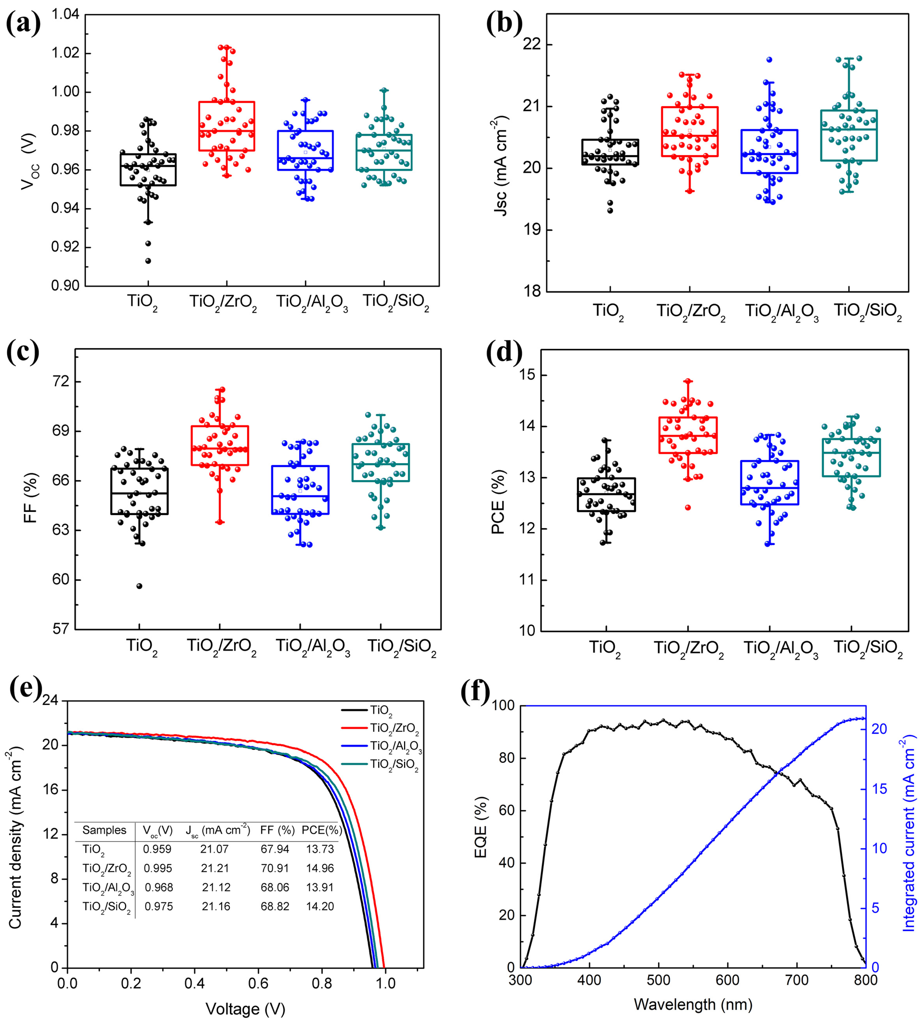
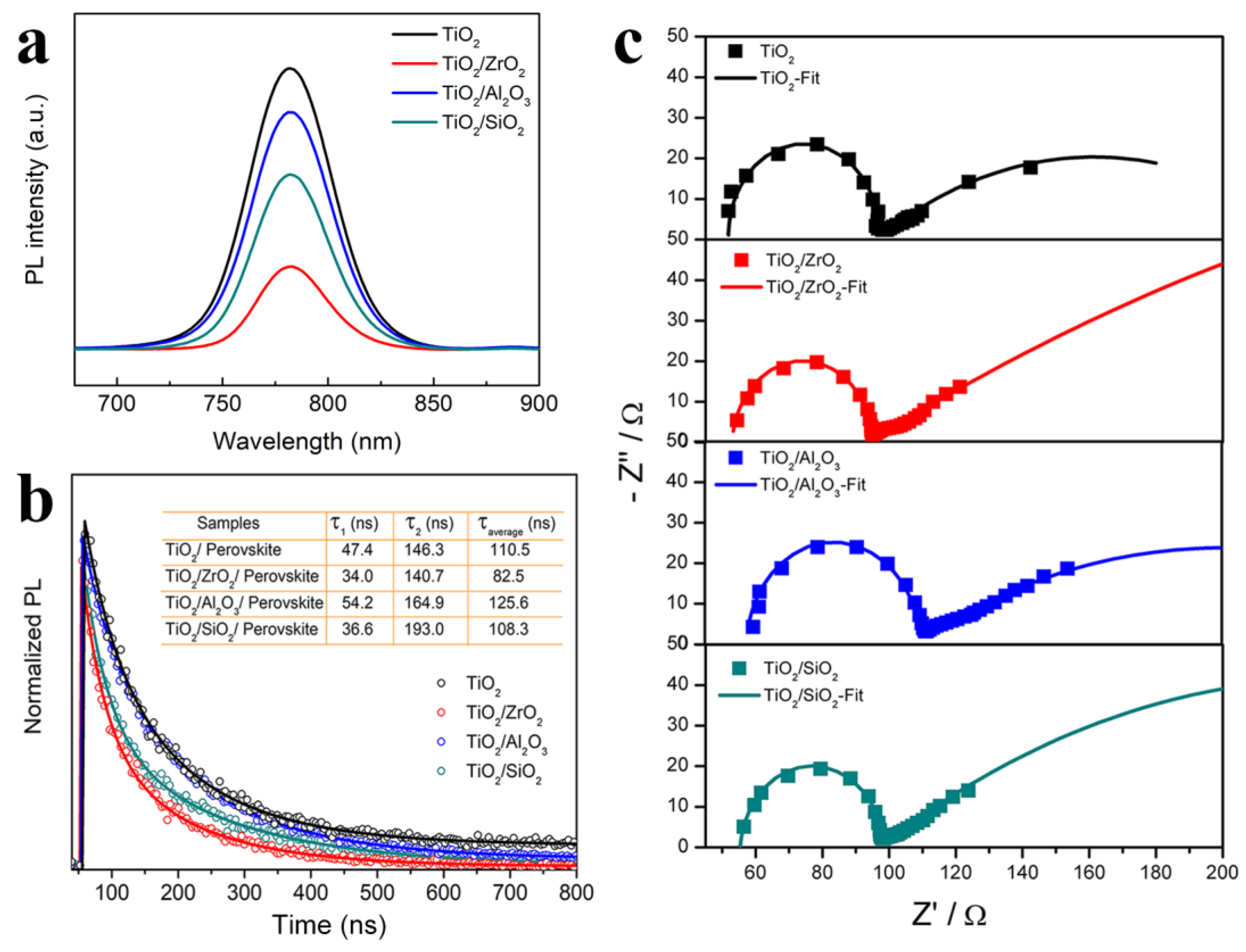
Figure 1. (a) Schematic illustration of the C−PSCs structure; (b) energy−level diagram of a C−PSC with ZrO2 as a TOP layer.
Nanomaterials 13 02640 g001
Figure 2. Dependence of Voc, Jsc, FF and PCE on the concentration of (a) ZrO2 paste and (b) Al2O3 paste.
Nanomaterials 13 02640 g002
Figure 3. (a) Cross-sectional SEM image of the PSC device; (b) cross-section SEM image of perovskite grown on TiO2/ZrO2 layer.
Nanomaterials 13 02640 g003
Figure 4. (ad) Plane-view SEM images of TiO2 film, TiO2/ZrO2 film, TiO2/Al2O3 film and TiO2/SiO2 film (left column) and the corresponding perovskites grown on them (right column); (e) XRD patterns of TiO2, TiO2/ZrO2, TiO2/Al2O3 and TiO2/SiO2 films (left) and the corresponding perovskite films (right) coated on them.
Nanomaterials 13 02640 g004
Figure 5. UV-vis absorption spectra of (a) TiO2, TiO2/ZrO2, TiO2/Al2O3 and TiO2/SiO2 films, (b) perovskite films coated on TiO2, TiO2/ZrO2, TiO2/Al2O3 and TiO2/SiO2.
Nanomaterials 13 02640 g005
Figure 6. Statistics of (a) Voc, (b) Jsc, (c) FF and (d) PCE for C−PSCs prepared using TiO2, TiO2/ZrO2, TiO2/Al2O3 andTiO2/SiO2 as scaffold layer (40 cells for each kind of devices); (e) J−V curves of the champion C−PSCs with various insulating layers; (f) incident photon-to-electron conversion efficiency (IPCE) spectrum and corresponding integrated current for the device based on TiO2/ZrO2.
Nanomaterials 13 02640 g006
Figure 7. (a) Steady-state photoluminescence (PL) spectra and (b) time-resolved photoluminescence (TRPL) spectra of MAPbI3 films deposited on various scaffolds; (c) EIS spectra and their fitting curves of C−PSCs based on various insulating layers.
Nanomaterials 13 02640 g007
Figure 8. Steady-state photocurrent and PCE output as a function of time held at a bias of 0.80 V under one-sun (100 mW cm−2) illumination for the device based on (a) TiO2/ZrO2 and (b) pristine TiO2.
Nanomaterials 13 02640 g008
Figure 9. Photovoltaic parameters versus storage time for a TiO2/ZrO2/MAPbI3/carbon solar cell stored under dry air with humidity of 50% at room temperature without encapsulation.
Nanomaterials 13 02640 g009
Table 1. Average photovoltaic parameters of total of 160 C-PSCs prepared with different scaffold layers. The error values represent the standard deviations.
Scaffold LayerVoc (V)Jsc (mA/cm2)FF (%)PCE (%)
TiO20.959 ± 0.01520.29 ± 0.4265.25 ± 1.8212.71 ± 0.45
TiO2/ZrO20.985 ± 0.01820.61 ± 0.4768.18 ± 1.6313.84 ± 0.53
TiO2/Al2O30.969 ± 0.01420.34 ± 0.5465.39 ± 1.8312.89 ± 0.56
TiO2/SiO20.971 ± 0.01320.63 ± 0.5665.39 ± 1.8313.42 ± 0.48
Table 2. Impendence values of PSCs with different insulating layers.
SamplesRs (Ω)Rct (Ω)Rrec (Ω)
TiO252.044.6126.5
TiO2/ZrO253.240.5630
TiO2/Al2O357.150.4185
TiO2/SiO255.342.1280
Disclaimer/Publisher’s Note: The statements, opinions and data contained in all publications are solely those of the individual author(s) and contributor(s) and not of MDPI and/or the editor(s). MDPI and/or the editor(s) disclaim responsibility for any injury to people or property resulting from any ideas, methods, instructions or products referred to in the content.

