
Recent Progress of Wide Bandgap Perovskites towards Two-Terminal Perovskite/Silicon Tandem Solar Cells


 , , ,
, , ,  and
and
Abstract
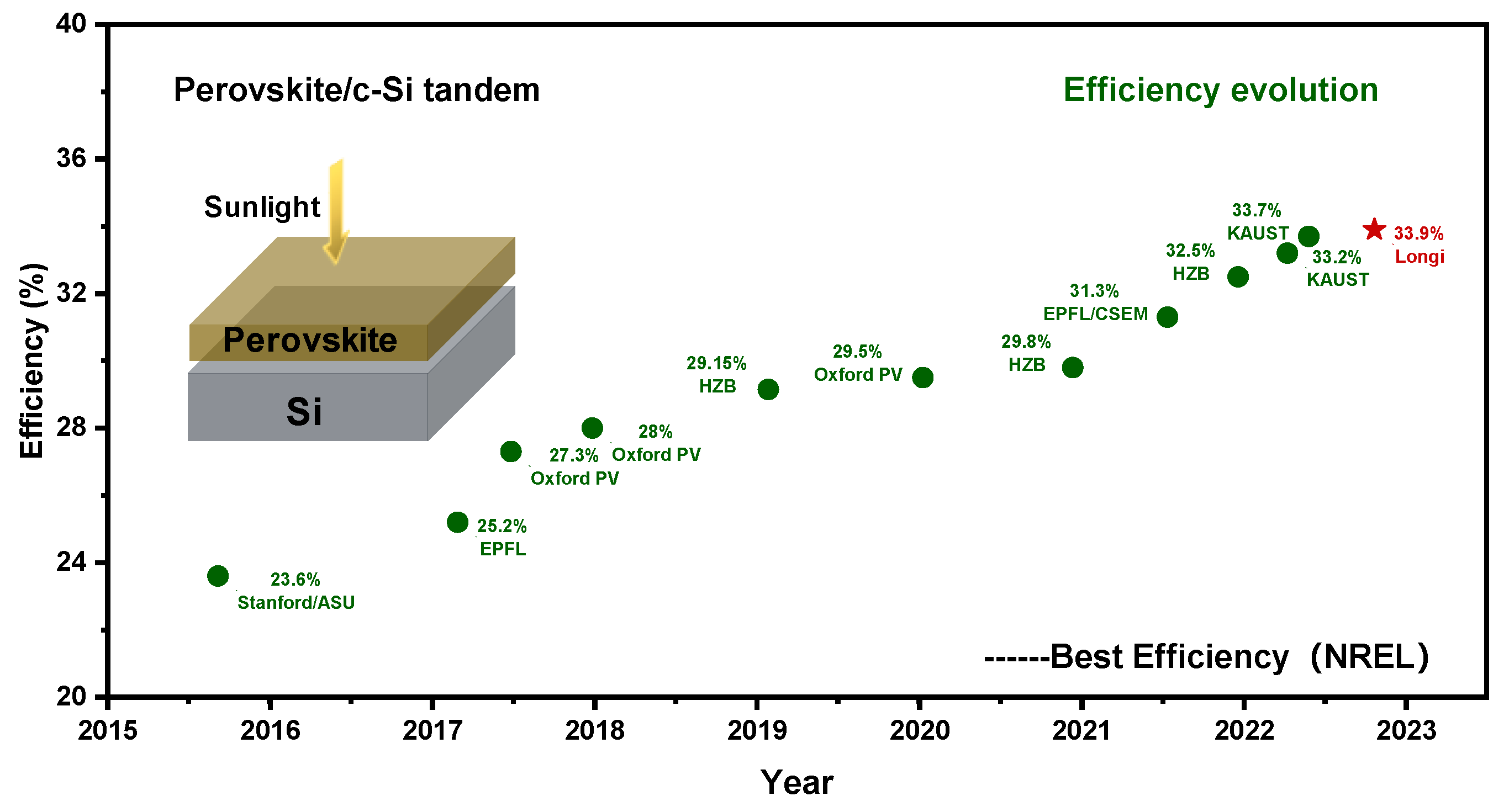
:1. Introduction
2. Compositional Engineering

| Absorber | Eg (eV) | Voc (V) | Jsc (mAcm−2) | FF (%) | PCE (%) | Year | Ref |
|---|---|---|---|---|---|---|---|
| (FAPbI3)0.8(MAPbBr3)0.2 | 1.67 | 1.14 | 21.15 | 77.49 | 18.68 | 2019 | [26] |
| FA0.65MA0.20Cs0.15Pb(I0.8Br0.2)3 | 1.68 | 1.17 | 21.2 | 79.8 | 19.8 | 2019 | [28] |
| Cs0.05(FA0.85MA0.15)0.95Pb(I0.85Br0.15)3 | 1.62 | 1.135 | 22.8 | 78 | 20.25 | 2019 | [29] |
| MA0.9FA0.1Pb(I0.6Br0.4)3 | 1.81 | 1.21 | 17.8 | 79.5 | 17.1 | 2020 | [10] |
| Cs0.05FA0.79MA0.16Pb(I0.6Br0.4)3 | 1.75 | 1.26 | 19.19 | 76 | 18.38 | 2020 | [30] |
| FA0.65MA0.20Cs0.15Pb(I0.8Br0.2)3 | 1.68 | 1.20 | / | / | 20.7 | 2020 | [31] |
| Cs0.05(FA0.77MA0.23)0.95Pb(I0.77Br0.23)3 | 1.68 | 1.22 | 20.7 | 82.0 | 20.8 | 2020 | [32] |
| FA0.64MA0.20Cs0.15Pb0.99(I0.79Br0.2)3 | 1.68 | 1.196 | 21.65 | 81.5 | 21.10 | 2020 | [33] |
| FA0.75MA0.15Cs0.1Rb0.05PbI2Br | 1.72 | 1.28 | 18.9 | 78.8 | 19.1 | 2021 | [34] |
| Cs0.15MA0.15FA0.7Pb(I0.8Br0.2)3 | 1.68 | 1.22 | / | / | 20.5 | 2021 | [35] |
| FA0.75MA0.15Cs0.1PbI2Br | 1.74 | 1.19 | 18.69 | 78.21 | 17.32 | 2022 | [36] |
| MA0.96FA0.1PbI2Br(SCN)0.12 | 1.72 | 1.19 | 18.65 | 78.4 | 17.40 | 2022 | [37] |
| Cs0.1FA0.2MA0.7Pb(I0.85Br0.15)3 | 1.65 | 1.23 | 21.2 | 83.8 | 21.90 | 2022 | [38] |
| FA0.8Cs0.15MA0.05Pb(I0.82Br0.18)3 | 1.65 | 1.221 | 21.5 | 83.3 | 21.90 | 2022 | [39] |
| FAMACsPb(I0.7Br0.3)3 | 1.73 | 1.3 | 19.68 | 83.27 | 21.33 | 2023 | [40] |
| FAMACsPb(I0.6Br0.4)3 | 1.79 | 1.34 | 17.80 | 83.10 | 19.53 | 2023 | [40] |
| FAMACsPb(I0.5Br0.5)3 | 1.85 | 1.36 | 16.21 | 83.21 | 18.14 | 2023 | [40] |
| FAMACsPb(I0.4Br0.6)3 | 1.92 | 1.39 | 14.30 | 83.47 | 16.23 | 2023 | [40] |
3. Additive Engineering
4. Interface Modification
5. Wide Bandgap Perovskites/Silicon Tandem
6. Conclusions and Outlook
Author Contributions
Funding
Data Availability Statement
Conflicts of Interest
References
- Rühle, S. Tabulated Values of the Shockley–Queisser Limit for Single Junction Solar Cells. Sol. Energy 2016, 130, 139–147. [Google Scholar] [CrossRef]
- Pazos-Outón, L.M.; Xiao, T.P.; Yablonovitch, E. Fundamental Efficiency Limit of Lead Iodide Perovskite Solar Cells. J. Phys. Chem. Lett. 2018, 9, 1703–1711. [Google Scholar] [CrossRef] [PubMed]
- Lin, H.; Yang, M.; Ru, X.; Wang, G.; Yin, S.; Peng, F.; Hong, C.; Qu, M.; Lu, J.; Fang, L.; et al. Silicon Heterojunction Solar Cells with up to 26.81% Efficiency Achieved by Electrically Optimized Nanocrystalline-Silicon Hole Contact Layers. Nat. Energy 2023, 8, 789–799. [Google Scholar] [CrossRef]
- Chen, J.; Park, N. Causes and Solutions of Recombination in Perovskite Solar Cells. Adv. Mater. 2019, 31, 1803019. [Google Scholar] [CrossRef]
- Jacak, J.E.; Jacak, W.A. Routes for Metallization of Perovskite Solar Cells. Materials 2022, 15, 2254. [Google Scholar] [CrossRef] [PubMed]
- Green, M.A.; Dunlop, E.D.; Yoshita, M.; Kopidakis, N.; Bothe, K.; Siefer, G.; Hao, X. Solar Cell Efficiency Tables (Version 63). Prog. Photovolt. Res. Appl. 2024, 32, 3–13. [Google Scholar] [CrossRef]
- Fu, F.; Li, J.; Yang, T.C.; Liang, H.; Faes, A.; Jeangros, Q.; Ballif, C.; Hou, Y. Monolithic Perovskite-Silicon Tandem Solar Cells: From the Lab to Fab? Adv. Mater. 2022, 34, 2106540. [Google Scholar] [CrossRef]
- Ugur, E.; Ledinský, M.; Allen, T.G.; Holovský, J.; Vlk, A.; De Wolf, S. Life on the Urbach Edge. J. Phys. Chem. Lett. 2022, 13, 7702–7711. [Google Scholar] [CrossRef]
- Liu, Y.; Banon, J.-P.; Frohna, K.; Chiang, Y.-H.; Tumen-Ulzii, G.; Stranks, S.D.; Filoche, M.; Friend, R.H. The Electronic Disorder Landscape of Mixed Halide Perovskites. ACS Energy Lett. 2023, 8, 250–258. [Google Scholar] [CrossRef]
- Xie, Y.; Zeng, Z.; Xu, X.; Ma, C.; Ma, Y.; Li, M.; Lee, C.; Tsang, S. FA-Assistant Iodide Coordination in Organic–Inorganic Wide-Bandgap Perovskite with Mixed Halides. Small 2020, 16, e1907226. [Google Scholar] [CrossRef]
- Löper, P.; Moon, S.-J.; Martín de Nicolas, S.; Niesen, B.; Ledinsky, M.; Nicolay, S.; Bailat, J.; Yum, J.-H.; De Wolf, S.; Ballif, C. Organic–Inorganic Halide Perovskite/Crystalline Silicon Four-Terminal Tandem Solar Cells. Phys. Chem. Chem. Phys. 2015, 17, 1619–1629. [Google Scholar] [CrossRef]
- Green, M.A.; Dunlop, E.D.; Yoshita, M.; Kopidakis, N.; Bothe, K.; Siefer, G.; Hao, X. Solar Cell Efficiency Tables (Version 62). Prog. Photovolt. Res. Appl. 2023, 31, 651–663. [Google Scholar] [CrossRef]
- Raza, E.; Ahmad, Z. Review on Two-Terminal and Four-Terminal Crystalline-Silicon/Perovskite Tandem Solar Cells; Progress, Challenges, and Future Perspectives. Energy Rep. 2022, 8, 5820–5851. [Google Scholar] [CrossRef]
- Li, H.; Zhang, W. Perovskite Tandem Solar Cells: From Fundamentals to Commercial Deployment. Chem. Rev. 2020, 120, 9835–9950. [Google Scholar] [CrossRef]
- Leijtens, T.; Bush, K.A.; Prasanna, R.; McGehee, M.D. Opportunities and Challenges for Tandem Solar Cells Using Metal Halide Perovskite Semiconductors. Nat. Energy 2018, 3, 828–838. [Google Scholar] [CrossRef]
- Suri, M.; Hazarika, A.; Larson, B.W.; Zhao, Q.; Vallés-Pelarda, M.; Siegler, T.D.; Abney, M.K.; Ferguson, A.J.; Korgel, B.A.; Luther, J.M. Enhanced Open-Circuit Voltage of Wide-Bandgap Perovskite Photovoltaics by Using Alloyed (FA1–xCsx)Pb(I1–xBrx) 3 Quantum Dots. ACS Energy Lett. 2019, 4, 1954–1960. [Google Scholar] [CrossRef]
- Matondo, J.T.; Malouangou, M.D.; Bai, L.; Yang, Y.; Zhang, Y.; Mbumba, M.T.; Akram, M.W.; Guli, M. Improving the Properties of MA-Based Wide-Bandgap Perovskite by Simple Precursor Salts Engineering for Efficiency and Ambient Stability Improvement in Solar Cells. Sol. Energy Mater. Sol. Cells 2022, 238, 111617. [Google Scholar] [CrossRef]
- Bi, C.; Yuan, Y.; Fang, Y.; Huang, J. Low-Temperature Fabrication of Efficient Wide-Bandgap Organolead Trihalide Perovskite Solar Cells. Adv. Energy Mater. 2015, 5, 1401616. [Google Scholar] [CrossRef]
- Hu, M.; Bi, C.; Yuan, Y.; Bai, Y.; Huang, J. Stabilized Wide Bandgap MAPbBr x I 3– x Perovskite by Enhanced Grain Size and Improved Crystallinity. Adv. Sci. 2016, 3, 1500301. [Google Scholar] [CrossRef]
- Xie, Y.-M.; Xu, X.; Ma, C.; Li, M.; Ma, Y.; Lee, C.-S.; Tsang, S.-W. Synergistic Effect of Pseudo-Halide Thiocyanate Anion and Cesium Cation on Realizing High-Performance Pinhole-Free MA-Based Wide-Band Gap Perovskites. ACS Appl. Mater. Interfaces 2019, 11, 25909–25916. [Google Scholar] [CrossRef]
- Chen, B.; Yu, Z.J.; Manzoor, S.; Wang, S.; Weigand, W.; Yu, Z.; Yang, G.; Ni, Z.; Dai, X.; Holman, Z.C.; et al. Blade-Coated Perovskites on Textured Silicon for 26%-Efficient Monolithic Perovskite/Silicon Tandem Solar Cells. Joule 2020, 4, 850–864. [Google Scholar] [CrossRef]
- Subbiah, A.S.; Isikgor, F.H.; Howells, C.T.; De Bastiani, M.; Liu, J.; Aydin, E.; Furlan, F.; Allen, T.G.; Xu, F.; Zhumagali, S.; et al. High-Performance Perovskite Single-Junction and Textured Perovskite/Silicon Tandem Solar Cells via Slot-Die-Coating. ACS Energy Lett. 2020, 5, 3034–3040. [Google Scholar] [CrossRef]
- Tao, L.; Du, X.; Hu, J.; Wang, S.; Lin, C.; Wei, Q.; Xia, Y.; Xing, G.; Chen, Y. Stabilizing Wide-Bandgap Halide Perovskites through Hydrogen Bonding. Sci. China Chem. 2022, 65, 1650–1660. [Google Scholar] [CrossRef]
- Tao, L.; Qiu, J.; Sun, B.; Wang, X.; Ran, X.; Song, L.; Shi, W.; Zhong, Q.; Li, P.; Zhang, H.; et al. Stability of Mixed-Halide Wide Bandgap Perovskite Solar Cells: Strategies and Progress. J. Energy Chem. 2021, 61, 395–415. [Google Scholar] [CrossRef]
- Jeon, N.J.; Noh, J.H.; Yang, W.S.; Kim, Y.C.; Ryu, S.; Seo, J.; Seok, S. Il Compositional Engineering of Perovskite Materials for High-Performance Solar Cells. Nature 2015, 517, 476–480. [Google Scholar] [CrossRef]
- Kim, C.U.; Yu, J.C.; Jung, E.D.; Choi, I.Y.; Park, W.; Lee, H.; Kim, I.; Lee, D.-K.; Hong, K.K.; Song, M.H.; et al. Optimization of Device Design for Low Cost and High Efficiency Planar Monolithic Perovskite/Silicon Tandem Solar Cells. Nano Energy 2019, 60, 213–221. [Google Scholar] [CrossRef]
- Jesper Jacobsson, T.; Correa-Baena, J.-P.; Pazoki, M.; Saliba, M.; Schenk, K.; Grätzel, M.; Hagfeldt, A. Exploration of the Compositional Space for Mixed Lead Halogen Perovskites for High Efficiency Solar Cells. Energy Environ. Sci. 2016, 9, 1706–1724. [Google Scholar] [CrossRef]
- Kim, D.H.; Muzzillo, C.P.; Tong, J.; Palmstrom, A.F.; Larson, B.W.; Choi, C.; Harvey, S.P.; Glynn, S.; Whitaker, J.B.; Zhang, F.; et al. Bimolecular Additives Improve Wide-Band-Gap Perovskites for Efficient Tandem Solar Cells with CIGS. Joule 2019, 3, 1734–1745. [Google Scholar] [CrossRef]
- Zheng, F.; Chen, W.; Bu, T.; Ghiggino, K.P.; Huang, F.; Cheng, Y.; Tapping, P.; Kee, T.W.; Jia, B.; Wen, X. Triggering the Passivation Effect of Potassium Doping in Mixed-Cation Mixed-Halide Perovskite by Light Illumination. Adv. Energy Mater. 2019, 9, 1901016. [Google Scholar] [CrossRef]
- Wang, L.; Wang, G.; Yan, Z.; Qiu, J.; Jia, C.; Zhang, W.; Zhen, C.; Xu, C.; Tai, K.; Jiang, X.; et al. Potassium-Induced Phase Stability Enables Stable and Efficient Wide-Bandgap Perovskite Solar Cells. Sol. RRL 2020, 4, 2000098. [Google Scholar] [CrossRef]
- Kim, D.; Jung, H.J.; Park, I.J.; Larson, B.W.; Dunfield, S.P.; Xiao, C.; Kim, J.; Tong, J.; Boonmongkolras, P.; Ji, S.G.; et al. Efficient, Stable Silicon Tandem Cells Enabled by Anion-Engineered Wide-Bandgap Perovskites. Science 2020, 368, 155–160. [Google Scholar] [CrossRef] [PubMed]
- Al-Ashouri, A.; Köhnen, E.; Li, B.; Magomedov, A.; Hempel, H.; Caprioglio, P.; Márquez, J.A.; Morales Vilches, A.B.; Kasparavicius, E.; Smith, J.A.; et al. Monolithic Perovskite/Silicon Tandem Solar Cell with >29% Efficiency by Enhanced Hole Extraction. Science 2020, 370, 1300–1309. [Google Scholar] [CrossRef] [PubMed]
- Ye, J.Y.; Tong, J.; Hu, J.; Xiao, C.; Lu, H.; Dunfield, S.P.; Kim, D.H.; Chen, X.; Larson, B.W.; Hao, J.; et al. Enhancing Charge Transport of 2D Perovskite Passivation Agent for Wide-Bandgap Perovskite Solar Cells Beyond 21%. Sol. RRL 2020, 4, 2000082. [Google Scholar] [CrossRef]
- Duong, T.; Pham, H.; Yin, Y.; Peng, J.; Mahmud, M.A.; Wu, Y.; Shen, H.; Zheng, J.; Tran-Phu, T.; Lu, T.; et al. Efficient and Stable Wide Bandgap Perovskite Solar Cells through Surface Passivation with Long Alkyl Chain Organic Cations. J. Mater. Chem. A 2021, 9, 18454–18465. [Google Scholar] [CrossRef]
- Isikgor, F.H.; Furlan, F.; Liu, J.; Ugur, E.; Eswaran, M.K.; Subbiah, A.S.; Yengel, E.; De Bastiani, M.; Harrison, G.T.; Zhumagali, S.; et al. Concurrent Cationic and Anionic Perovskite Defect Passivation Enables 27.4% Perovskite/Silicon Tandems with Suppression of Halide Segregation. Joule 2021, 5, 1566–1586. [Google Scholar] [CrossRef]
- Huo, X.; Li, Y.; Lu, Y.; Dong, J.; Zhang, Y.; Zhao, S.; Qiao, B.; Wei, D.; Song, D.; Xu, Z. Suppressed Halide Segregation and Defects in Wide Bandgap Perovskite Solar Cells Enabled by Doping Organic Bromide Salt with Moderate Chain Length. J. Phys. Chem. C 2022, 126, 1711–1720. [Google Scholar] [CrossRef]
- Xie, Y.; Yao, Q.; Zeng, Z.; Xue, Q.; Niu, T.; Xia, R.; Cheng, Y.; Lin, F.; Tsang, S.; Jen, A.K.-Y.; et al. Homogeneous Grain Boundary Passivation in Wide-Bandgap Perovskite Films Enables Fabrication of Monolithic Perovskite/Organic Tandem Solar Cells with over 21% Efficiency. Adv. Funct. Mater. 2022, 32, 2112126. [Google Scholar] [CrossRef]
- Yang, G.; Ni, Z.; Yu, Z.J.; Larson, B.W.; Yu, Z.; Chen, B.; Alasfour, A.; Xiao, X.; Luther, J.M.; Holman, Z.C.; et al. Defect Engineering in Wide-Bandgap Perovskites for Efficient Perovskite–Silicon Tandem Solar Cells. Nat. Photonics 2022, 16, 588–594. [Google Scholar] [CrossRef]
- Liu, Z.; Zhu, C.; Luo, H.; Kong, W.; Luo, X.; Wu, J.; Ding, C.; Chen, Y.; Wang, Y.; Wen, J.; et al. Grain Regrowth and Bifacial Passivation for High-Efficiency Wide-Bandgap Perovskite Solar Cells. Adv. Energy Mater. 2023, 13, 2203230. [Google Scholar] [CrossRef]
- An, Y.; Zhang, N.; Zeng, Z.; Cai, Y.; Jiang, W.; Qi, F.; Ke, L.; Lin, F.R.; Tsang, S.; Shi, T.; et al. Optimizing Crystallization in Wide-Bandgap Mixed Halide Perovskites for High-Efficiency Solar Cells. Adv. Mater. 2023, 2306568. [Google Scholar] [CrossRef]
- McMeekin, D.P.; Sadoughi, G.; Rehman, W.; Eperon, G.E.; Saliba, M.; Hörantner, M.T.; Haghighirad, A.; Sakai, N.; Korte, L.; Rech, B.; et al. A Mixed-Cation Lead Mixed-Halide Perovskite Absorber for Tandem Solar Cells. Science 2016, 351, 151–155. [Google Scholar] [CrossRef] [PubMed]
- Ou, Y.; Huang, H.; Shi, H.; Li, Z.; Chen, Z.; Mateen, M.; Lu, Z.; Chi, D.; Huang, S. Collaborative Interfacial Modification and Surficial Passivation for High-Efficiency MA-Free Wide-Bandgap Perovskite Solar Cells. Chem. Eng. J. 2023, 469, 143860. [Google Scholar] [CrossRef]
- Gharibzadeh, S.; Abdollahi Nejand, B.; Jakoby, M.; Abzieher, T.; Hauschild, D.; Moghadamzadeh, S.; Schwenzer, J.A.; Brenner, P.; Schmager, R.; Haghighirad, A.A.; et al. Record Open-Circuit Voltage Wide-Bandgap Perovskite Solar Cells Utilizing 2D/3D Perovskite Heterostructure. Adv. Energy Mater. 2019, 9, 1803699. [Google Scholar] [CrossRef]
- Yu, Z.; Yang, Z.; Ni, Z.; Shao, Y.; Chen, B.; Lin, Y.; Wei, H.; Yu, Z.J.; Holman, Z.; Huang, J. Simplified Interconnection Structure Based on C60/SnO2-x for All-Perovskite Tandem Solar Cells. Nat. Energy 2020, 5, 657–665. [Google Scholar] [CrossRef]
- Liang, J.; Chen, C.; Hu, X.; Chen, Z.; Zheng, X.; Li, J.; Wang, H.; Ye, F.; Xiao, M.; Lu, Z.; et al. Suppressing the Phase Segregation with Potassium for Highly Efficient and Photostable Inverted Wide-Band Gap Halide Perovskite Solar Cells. ACS Appl. Mater. Interfaces 2020, 12, 48458–48466. [Google Scholar] [CrossRef] [PubMed]
- Xu, J.; Boyd, C.C.; Yu, Z.J.; Palmstrom, A.F.; Witter, D.J.; Larson, B.W.; France, R.M.; Werner, J.; Harvey, S.P.; Wolf, E.J.; et al. Triple-Halide Wide–Band Gap Perovskites with Suppressed Phase Segregation for Efficient Tandems. Science 2020, 367, 1097–1104. [Google Scholar] [CrossRef] [PubMed]
- Wang, Y.; Gu, S.; Liu, G.; Zhang, L.; Liu, Z.; Lin, R.; Xiao, K.; Luo, X.; Shi, J.; Du, J.; et al. Cross-Linked Hole Transport Layers for High-Efficiency Perovskite Tandem Solar Cells. Sci. China Chem. 2021, 64, 2025–2034. [Google Scholar] [CrossRef]
- Wang, D.; Guo, H.; Wu, X.; Deng, X.; Li, F.; Li, Z.; Lin, F.; Zhu, Z.; Zhang, Y.; Xu, B.; et al. Interfacial Engineering of Wide-Bandgap Perovskites for Efficient Perovskite/CZTSSe Tandem Solar Cells. Adv. Funct. Mater. 2022, 32, 2107359. [Google Scholar] [CrossRef]
- Chen, C.; Liang, J.; Zhang, J.; Liu, X.; Yin, X.; Cui, H.; Wang, H.; Wang, C.; Li, Z.; Gong, J.; et al. Interfacial Engineering of a Thiophene-Based 2D/3D Perovskite Heterojunction for Efficient and Stable Inverted Wide-Bandgap Perovskite Solar Cells. Nano Energy 2021, 90, 106608. [Google Scholar] [CrossRef]
- Fang, Z.; Jia, L.; Yan, N.; Jiang, X.; Ren, X.; Yang, S.; Liu, S. (Frank) Proton-transfer-induced in Situ Defect Passivation for Highly Efficient Wide-bandgap Inverted Perovskite Solar Cells. InfoMat 2022, 4, e12307. [Google Scholar] [CrossRef]
- Oliver, R.D.J.; Caprioglio, P.; Peña-Camargo, F.; Buizza, L.R.V.; Zu, F.; Ramadan, A.J.; Motti, S.G.; Mahesh, S.; McCarthy, M.M.; Warby, J.H.; et al. Understanding and Suppressing Non-Radiative Losses in Methylammonium-Free Wide-Bandgap Perovskite Solar Cells. Energy Environ. Sci. 2022, 15, 714–726. [Google Scholar] [CrossRef]
- Wang, L.; Song, Q.; Pei, F.; Chen, Y.; Dou, J.; Wang, H.; Shi, C.; Zhang, X.; Fan, R.; Zhou, W.; et al. Strain Modulation for Light-Stable n–i–p Perovskite/Silicon Tandem Solar Cells. Adv. Mater. 2022, 34, 2201315. [Google Scholar] [CrossRef]
- Mahmud, M.A.; Zheng, J.; Tang, S.; Wang, G.; Bing, J.; Bui, A.D.; Qu, J.; Yang, L.; Liao, C.; Chen, H.; et al. Cation-Diffusion-Based Simultaneous Bulk and Surface Passivations for High Bandgap Inverted Perovskite Solar Cell Producing Record Fill Factor and Efficiency. Adv. Energy Mater. 2022, 12, 2201672. [Google Scholar] [CrossRef]
- Zhu, Z.; Mao, K.; Zhang, K.; Peng, W.; Zhang, J.; Meng, H.; Cheng, S.; Li, T.; Lin, H.; Chen, Q.; et al. Correlating the Perovskite/Polymer Multi-Mode Reactions with Deep-Level Traps in Perovskite Solar Cells. Joule 2022, 6, 2849–2868. [Google Scholar] [CrossRef]
- Li, R.; Chen, B.; Ren, N.; Wang, P.; Shi, B.; Xu, Q.; Zhao, H.; Han, W.; Zhu, Z.; Liu, J.; et al. CsPbCl3-Cluster-Widened Bandgap and Inhibited Phase Segregation in a Wide-Bandgap Perovskite and Its Application to NiOx-Based Perovskite/Silicon Tandem Solar Cells. Adv. Mater. 2022, 34, 2201451. [Google Scholar] [CrossRef]
- Chen, H.; Maxwell, A.; Li, C.; Teale, S.; Chen, B.; Zhu, T.; Ugur, E.; Harrison, G.; Grater, L.; Wang, J.; et al. Regulating Surface Potential Maximizes Voltage in All-Perovskite Tandems. Nature 2023, 613, 676–681. [Google Scholar] [CrossRef] [PubMed]
- Shen, X.; Gallant, B.M.; Holzhey, P.; Smith, J.A.; Elmestekawy, K.A.; Yuan, Z.; Rathnayake, P.V.G.M.; Bernardi, S.; Dasgupta, A.; Kasparavicius, E.; et al. Chloride-Based Additive Engineering for Efficient and Stable Wide-Bandgap Perovskite Solar Cells. Adv. Mater. 2023, 35, 2211742. [Google Scholar] [CrossRef]
- Cao, W.; Lin, K.; Li, J.; Qiu, L.; Dong, Y.; Wang, J.; Xia, D.; Fan, R.; Yang, Y. Iodine-Doped Graphite Carbon Nitride for Enhancing Photovoltaic Device Performance via Passivation Trap States of Triple Cation Perovskite Films. J. Mater. Chem. C 2019, 7, 12717–12724. [Google Scholar] [CrossRef]
- Zhou, X.; Qiu, L.; Fan, R.; Zhang, J.; Hao, S.; Yang, Y. Heterojunction Incorporating Perovskite and Microporous Metal–Organic Framework Nanocrystals for Efficient and Stable Solar Cells. Nano-Micro Lett. 2020, 12, 80. [Google Scholar] [CrossRef]
- Kim, J.; Kim, Y.R.; Park, B.; Hong, S.; Hwang, I.; Kim, J.; Kwon, S.; Kim, G.; Kim, H.; Lee, K. Simultaneously Passivating Cation and Anion Defects in Metal Halide Perovskite Solar Cells Using a Zwitterionic Amino Acid Additive. Small 2021, 17, e2005608. [Google Scholar] [CrossRef]
- Tan, H.; Che, F.; Wei, M.; Zhao, Y.; Saidaminov, M.I.; Todorović, P.; Broberg, D.; Walters, G.; Tan, F.; Zhuang, T.; et al. Dipolar Cations Confer Defect Tolerance in Wide-Bandgap Metal Halide Perovskites. Nat. Commun. 2018, 9, 3100. [Google Scholar] [CrossRef] [PubMed]
- Beal, R.E.; Hagström, N.Z.; Barrier, J.; Gold-Parker, A.; Prasanna, R.; Bush, K.A.; Passarello, D.; Schelhas, L.T.; Brüning, K.; Tassone, C.J.; et al. Structural Origins of Light-Induced Phase Segregation in Organic-Inorganic Halide Perovskite Photovoltaic Materials. Matter 2020, 2, 207–219. [Google Scholar] [CrossRef]
- Brennan, M.C.; Ruth, A.; Kamat, P.V.; Kuno, M. Photoinduced Anion Segregation in Mixed Halide Perovskites. Trends Chem. 2020, 2, 282–301. [Google Scholar] [CrossRef]
- Abdi-Jalebi, M.; Andaji-Garmaroudi, Z.; Cacovich, S.; Stavrakas, C.; Philippe, B.; Richter, J.M.; Alsari, M.; Booker, E.P.; Hutter, E.M.; Pearson, A.J.; et al. Maximizing and Stabilizing Luminescence from Halide Perovskites with Potassium Passivation. Nature 2018, 555, 497–501. [Google Scholar] [CrossRef]
- Qiao, L.; Ye, T.; Wang, P.; Wang, T.; Zhang, L.; Sun, R.; Kong, W.; Yang, X. Crystallization Enhancement and Ionic Defect Passivation in Wide-Bandgap Perovskite for Efficient and Stable All-Perovskite Tandem Solar Cells. Adv. Funct. Mater. 2023, 2308908. [Google Scholar] [CrossRef]
- Chen, H.; Xia, Y.; Wu, B.; Liu, F.; Niu, T.; Chao, L.; Xing, G.; Sum, T.; Chen, Y.; Huang, W. Critical Role of Chloride in Organic Ammonium Spacer on the Performance of Low-Dimensional Ruddlesden-Popper Perovskite Solar Cells. Nano Energy 2019, 56, 373–381. [Google Scholar] [CrossRef]
- Zhao, Y.; Wang, C.; Ma, T.; Zhou, L.; Wu, Z.; Wang, H.; Chen, C.; Yu, Z.; Sun, W.; Wang, A.; et al. Reduced 0.418 V V OC-Deficit of 1.73 EV Wide-Bandgap Perovskite Solar Cells Assisted by Dual Chlorides for Efficient All-Perovskite Tandems. Energy Environ. Sci. 2023, 16, 2080–2089. [Google Scholar] [CrossRef]
- Bai, Y.; Huang, Z.; Zhang, X.; Lu, J.; Niu, X.; He, Z.; Zhu, C.; Xiao, M.; Song, Q.; Wei, X.; et al. Initializing Film Homogeneity to Retard Phase Segregation for Stable Perovskite Solar Cells. Science 2022, 378, 747–754. [Google Scholar] [CrossRef]
- Xie, L.; Liu, J.; Li, J.; Liu, C.; Pu, Z.; Xu, P.; Wang, Y.; Meng, Y.; Yang, M.; Ge, Z. A Deformable Additive on Defects Passivation and Phase Segregation Inhibition Enables the Efficiency of Inverted Perovskite Solar Cells over 24%. Adv. Mater. 2023, 35, 2302752. [Google Scholar] [CrossRef]
- Liu, Y.; Gao, Y.; Lu, M.; Shi, Z.; Yu, W.W.; Hu, J.; Bai, X.; Zhang, Y. Ionic Additive Engineering for Stable Planar Perovskite Solar Cells with Efficiency >22%. Chem. Eng. J. 2021, 426, 130841. [Google Scholar] [CrossRef]
- Zhao, W.; Guo, P.; Su, J.; Fang, Z.; Jia, N.; Liu, C.; Ye, L.; Ye, Q.; Chang, J.; Wang, H. Synchronous Passivation of Defects with Low Formation Energies via Terdentate Anchoring Enabling High Performance Perovskite Solar Cells with Efficiency over 24%. Adv. Funct. Mater. 2022, 32, 2200534. [Google Scholar] [CrossRef]
- Zhang, Z.; Jiang, J.; Liu, X.; Wang, X.; Wang, L.; Qiu, Y.; Zhang, Z.; Zheng, Y.; Wu, X.; Liang, J.; et al. Surface-Anchored Acetylcholine Regulates Band-Edge States and Suppresses Ion Migration in a 21%-Efficient Quadruple-Cation Perovskite Solar Cell. Small 2022, 18, 2105184. [Google Scholar] [CrossRef]
- Chen, R.; Wang, Y.; Nie, S.; Shen, H.; Hui, Y.; Peng, J.; Wu, B.; Yin, J.; Li, J.; Zheng, N. Sulfonate-Assisted Surface Iodide Management for High-Performance Perovskite Solar Cells and Modules. J. Am. Chem. Soc. 2021, 143, 10624–10632. [Google Scholar] [CrossRef]
- Li, X.; Li, W.; Yang, Y.; Lai, X.; Su, Q.; Wu, D.; Li, G.; Wang, K.; Chen, S.; Sun, X.W.; et al. Defects Passivation With Dithienobenzodithiophene-based Π-conjugated Polymer for Enhanced Performance of Perovskite Solar Cells. Sol. RRL 2019, 3, 1900029. [Google Scholar] [CrossRef]
- Li, F.; Deng, X.; Qi, F.; Li, Z.; Liu, D.; Shen, D.; Qin, M.; Wu, S.; Lin, F.; Jang, S.-H.; et al. Regulating Surface Termination for Efficient Inverted Perovskite Solar Cells with Greater Than 23% Efficiency. J. Am. Chem. Soc. 2020, 142, 20134–20142. [Google Scholar] [CrossRef]
- Sun, S.; Xu, X.; Sun, Q.; Yao, Q.; Cai, Y.; Li, X.; Xu, Y.; He, W.; Zhu, M.; Lv, X.; et al. All-Inorganic Perovskite-Based Monolithic Perovskite/Organic Tandem Solar Cells with 23.21% Efficiency by Dual-Interface Engineering. Adv. Energy Mater. 2023, 13, 2204347. [Google Scholar] [CrossRef]
- Zong, B.; Hu, D.; Sun, Q.; Deng, J.; Zhang, Z.; Meng, X.; Shen, B.; Kang, B.; Silva, S.R.P.; Lu, G. 2, 3, 4, 5, 6-Pentafluorophenylammonium Bromide-Based Double-Sided Interface Engineering for Efficient Planar Heterojunction Perovskite Solar Cells. Chem. Eng. J. 2023, 452, 139308. [Google Scholar] [CrossRef]
- Mariotti, S.; Köhnen, E.; Scheler, F.; Sveinbjörnsson, K.; Zimmermann, L.; Piot, M.; Yang, F.; Li, B.; Warby, J.; Musiienko, A.; et al. Interface Engineering for High-Performance, Triple-Halide Perovskite–Silicon Tandem Solar Cells. Science 2023, 381, 63–69. [Google Scholar] [CrossRef]
- Li, Y.; Lim, E.L.; Xie, H.; Song, J.; Kong, T.; Zhang, Y.; Yang, M.; Wu, B.; Duan, C.; Bi, D. Hydrophobic Fluorinated Conjugated Polymer as a Multifunctional Interlayer for High-Performance Perovskite Solar Cells. ACS Photonics 2021, 8, 3185–3192. [Google Scholar] [CrossRef]
- Zheng, X.; Huang, Z.; Luo, X.; Wang, B.; Zhang, X.; Yang, G.; Feng, Z.; Chen, Y.; Kong, W.; Gao, J.; et al. Reducing Perovskite/C60 Interface Losses via Sequential Interface Engineering for Efficient Perovskite/Silicon Tandem Solar Cell. Adv. Mater. 2023, 2308370. [Google Scholar] [CrossRef]
- Mazzarella, L.; Lin, Y.; Kirner, S.; Morales-Vilches, A.B.; Korte, L.; Albrecht, S.; Crossland, E.; Stannowski, B.; Case, C.; Snaith, H.J.; et al. Infrared Light Management Using a Nanocrystalline Silicon Oxide Interlayer in Monolithic Perovskite/Silicon Heterojunction Tandem Solar Cells with Efficiency above 25%. Adv. Energy Mater. 2019, 9, 1803241. [Google Scholar] [CrossRef]
- Jošt, M.; Köhnen, E.; Morales-Vilches, A.B.; Lipovšek, B.; Jäger, K.; Macco, B.; Al-Ashouri, A.; Krč, J.; Korte, L.; Rech, B.; et al. Textured Interfaces in Monolithic Perovskite/Silicon Tandem Solar Cells: Advanced Light Management for Improved Efficiency and Energy Yield. Energy Environ. Sci. 2018, 11, 3511–3523. [Google Scholar] [CrossRef]
- Zheng, J.; Mehrvarz, H.; Liao, C.; Bing, J.; Cui, X.; Li, Y.; Gonçales, V.R.; Lau, C.F.J.; Lee, D.S.; Li, Y.; et al. Large-Area 23%-Efficient Monolithic Perovskite/Homojunction-Silicon Tandem Solar Cell with Enhanced UV Stability Using Down-Shifting Material. ACS Energy Lett. 2019, 4, 2623–2631. [Google Scholar] [CrossRef]
- Bett, A.J.; Schulze, P.S.C.; Winkler, K.M.; Kabakli, Ö.S.; Ketterer, I.; Mundt, L.E.; Reichmuth, S.K.; Siefer, G.; Cojocaru, L.; Tutsch, L.; et al. Two-terminal Perovskite Silicon Tandem Solar Cells with a High-Bandgap Perovskite Absorber Enabling Voltages over 1.8 V. Prog. Photovolt. Res. Appl. 2020, 28, 99–110. [Google Scholar] [CrossRef]
- Hou, Y.; Aydin, E.; De Bastiani, M.; Xiao, C.; Isikgor, F.H.; Xue, D.-J.; Chen, B.; Chen, H.; Bahrami, B.; Chowdhury, A.H.; et al. Efficient Tandem Solar Cells with Solution-Processed Perovskite on Textured Crystalline Silicon. Science 2020, 367, 1135–1140. [Google Scholar] [CrossRef] [PubMed]
- Schulze, P.S.C.; Bett, A.J.; Bivour, M.; Caprioglio, P.; Gerspacher, F.M.; Kabaklı, Ö.Ş.; Richter, A.; Stolterfoht, M.; Zhang, Q.; Neher, D.; et al. 25.1% High-Efficiency Monolithic Perovskite Silicon Tandem Solar Cell with a High Bandgap Perovskite Absorber. Sol. RRL 2020, 4, 2000152. [Google Scholar] [CrossRef]
- Green, M.; Dunlop, E.; Hohl-Ebinger, J.; Yoshita, M.; Kopidakis, N.; Hao, X. Solar Cell Efficiency Tables (Version 57). Prog. Photovolt. Res. Appl. 2021, 29, 3–15. [Google Scholar] [CrossRef]
- Köhnen, E.; Wagner, P.; Lang, F.; Cruz, A.; Li, B.; Roß, M.; Jošt, M.; Morales-Vilches, A.B.; Topič, M.; Stolterfoht, M.; et al. 27.9% Efficient Monolithic Perovskite/Silicon Tandem Solar Cells on Industry Compatible Bottom Cells. Sol. RRL 2021, 5, 2100244. [Google Scholar] [CrossRef]
- Aydin, E.; Liu, J.; Ugur, E.; Azmi, R.; Harrison, G.T.; Hou, Y.; Chen, B.; Zhumagali, S.; De Bastiani, M.; Wang, M.; et al. Ligand-Bridged Charge Extraction and Enhanced Quantum Efficiency Enable Efficient n–i–p Perovskite/Silicon Tandem Solar Cells. Energy Environ. Sci. 2021, 14, 4377–4390. [Google Scholar] [CrossRef]
- Zhumagali, S.; Isikgor, F.H.; Maity, P.; Yin, J.; Ugur, E.; De Bastiani, M.; Subbiah, A.S.; Mirabelli, A.J.; Azmi, R.; Harrison, G.T.; et al. Linked Nickel Oxide/Perovskite Interface Passivation for High-Performance Textured Monolithic Tandem Solar Cells. Adv. Energy Mater. 2021, 11, 2101662. [Google Scholar] [CrossRef]
- Li, Y.; Shi, B.; Xu, Q.; Yan, L.; Ren, N.; Chen, Y.; Han, W.; Huang, Q.; Zhao, Y.; Zhang, X. Wide Bandgap Interface Layer Induced Stabilized Perovskite/Silicon Tandem Solar Cells with Stability over Ten Thousand Hours. Adv. Energy Mater. 2021, 11, 2102046. [Google Scholar] [CrossRef]
- Liu, J.; Aydin, E.; Yin, J.; De Bastiani, M.; Isikgor, F.H.; Rehman, A.U.; Yengel, E.; Ugur, E.; Harrison, G.T.; Wang, M.; et al. 28.2%-Efficient, Outdoor-Stable Perovskite/Silicon Tandem Solar Cell. Joule 2021, 5, 3169–3186. [Google Scholar] [CrossRef]
- Wu, Y.; Zheng, P.; Peng, J.; Xu, M.; Chen, Y.; Surve, S.; Lu, T.; Bui, A.D.; Li, N.; Liang, W.; et al. 27.6% Perovskite/C-Si Tandem Solar Cells Using Industrial Fabricated TOPCon Device. Adv. Energy Mater. 2022, 12, 2200821. [Google Scholar] [CrossRef]
- Sveinbjörnsson, K.; Li, B.; Mariotti, S.; Jarzembowski, E.; Kegelmann, L.; Wirtz, A.; Frühauf, F.; Weihrauch, A.; Niemann, R.; Korte, L.; et al. Monolithic Perovskite/Silicon Tandem Solar Cell with 28.7% Efficiency Using Industrial Silicon Bottom Cells. ACS Energy Lett. 2022, 7, 2654–2656. [Google Scholar] [CrossRef]
- Mao, L.; Yang, T.; Zhang, H.; Shi, J.; Hu, Y.; Zeng, P.; Li, F.; Gong, J.; Fang, X.; Sun, Y.; et al. Fully Textured, Production-Line Compatible Monolithic Perovskite/Silicon Tandem Solar Cells Approaching 29% Efficiency. Adv. Mater. 2022, 34, 2206193. [Google Scholar] [CrossRef] [PubMed]
- Ying, Z.; Yang, Z.; Zheng, J.; Wei, H.; Chen, L.; Xiao, C.; Sun, J.; Shou, C.; Qin, G.; Sheng, J.; et al. Monolithic Perovskite/Black-Silicon Tandems Based on Tunnel Oxide Passivated Contacts. Joule 2022, 6, 2644–2661. [Google Scholar] [CrossRef]
- Tockhorn, P.; Sutter, J.; Cruz, A.; Wagner, P.; Jäger, K.; Yoo, D.; Lang, F.; Grischek, M.; Li, B.; Li, J.; et al. Nano-Optical Designs for High-Efficiency Monolithic Perovskite–Silicon Tandem Solar Cells. Nat. Nanotechnol. 2022, 17, 1214–1221. [Google Scholar] [CrossRef]
- Xu, Q.; Shi, B.; Li, Y.; Yan, L.; Duan, W.; Li, Y.; Li, R.; Ren, N.; Han, W.; Liu, J.; et al. Conductive Passivator for Efficient Monolithic Perovskite/Silicon Tandem Solar Cell on Commercially Textured Silicon. Adv. Energy Mater. 2022, 12, 2202404. [Google Scholar] [CrossRef]
- De Bastiani, M.; Jalmood, R.; Liu, J.; Ossig, C.; Vlk, A.; Vegso, K.; Babics, M.; Isikgor, F.H.; Selvin, A.S.; Azmi, R.; et al. Monolithic Perovskite/Silicon Tandems with >28% Efficiency: Role of Silicon-Surface Texture on Perovskite Properties. Adv. Funct. Mater. 2023, 33, 2205557. [Google Scholar] [CrossRef]
- Zheng, J.; Wei, H.; Ying, Z.; Yang, X.; Sheng, J.; Yang, Z.; Zeng, Y.; Ye, J. Balancing Charge-Carrier Transport and Recombination for Perovskite/TOPCon Tandem Solar Cells with Double-Textured Structures. Adv. Energy Mater. 2023, 13, 2203006. [Google Scholar] [CrossRef]
- Zheng, J.; Duan, W.; Guo, Y.; Zhao, Z.C.; Yi, H.; Ma, F.-J.; Granados Caro, L.; Yi, C.; Bing, J.; Tang, S.; et al. Efficient Monolithic Perovskite–Si Tandem Solar Cells Enabled by an Ultra-Thin Indium Tin Oxide Interlayer. Energy Environ. Sci. 2023, 16, 1223–1233. [Google Scholar] [CrossRef]
- Hang, P.; Kan, C.; Li, B.; Yao, Y.; Hu, Z.; Zhang, Y.; Xie, J.; Wang, Y.; Yang, D.; Yu, X. Highly Efficient and Stable Wide-Bandgap Perovskite Solar Cells via Strain Management. Adv. Funct. Mater. 2023, 33, 2214381. [Google Scholar] [CrossRef]
- Li, X.; Ying, Z.; Zheng, J.; Wang, X.; Chen, Y.; Wu, M.; Xiao, C.; Sun, J.; Shou, C.; Yang, Z.; et al. Surface Reconstruction for Efficient and Stable Monolithic Perovskite/Silicon Tandem Solar Cells with Greatly Suppressed Residual Strain. Adv. Mater. 2023, 35, 2211962. [Google Scholar] [CrossRef]
- Chin, X.Y.; Turkay, D.; Steele, J.A.; Tabean, S.; Eswara, S.; Mensi, M.; Fiala, P.; Wolff, C.M.; Paracchino, A.; Artuk, K.; et al. Interface Passivation for 31.25%-Efficient Perovskite/Silicon Tandem Solar Cells. Science 2023, 381, 59–63. [Google Scholar] [CrossRef] [PubMed]
- Zheng, J.; Ying, Z.; Yang, Z.; Lin, Z.; Wei, H.; Chen, L.; Yang, X.; Zeng, Y.; Li, X.; Ye, J. Polycrystalline Silicon Tunnelling Recombination Layers for High-Efficiency Perovskite/Tunnel Oxide Passivating Contact Tandem Solar Cells. Nat. Energy 2023, 8, 1250–1261. [Google Scholar] [CrossRef]
- Wang, G.; Zheng, J.; Duan, W.; Yang, J.; Mahmud, M.A.; Lian, Q.; Tang, S.; Liao, C.; Bing, J.; Yi, J.; et al. Molecular Engineering of Hole-Selective Layer for High Band Gap Perovskites for Highly Efficient and Stable Perovskite-Silicon Tandem Solar Cells. Joule 2023, 7, 2583–2594. [Google Scholar] [CrossRef]
- Luo, H.; Zheng, X.; Kong, W.; Liu, Z.; Li, H.; Wen, J.; Xia, R.; Sun, H.; Wu, P.; Wang, Y.; et al. Inorganic Framework Composition Engineering for Scalable Fabrication of Perovskite/Silicon Tandem Solar Cells. ACS Energy Lett. 2023, 8, 4993–5002. [Google Scholar] [CrossRef]
- Roß, M.; Severin, S.; Stutz, M.B.; Wagner, P.; Köbler, H.; Favin-Lévêque, M.; Al-Ashouri, A.; Korb, P.; Tockhorn, P.; Abate, A.; et al. Co-Evaporated Formamidinium Lead Iodide Based Perovskites with 1000 h Constant Stability for Fully Textured Monolithic Perovskite/Silicon Tandem Solar Cells. Adv. Energy Mater. 2021, 11, 2101460. [Google Scholar] [CrossRef]
- Sahli, F.; Werner, J.; Kamino, B.A.; Bräuninger, M.; Monnard, R.; Paviet-Salomon, B.; Barraud, L.; Ding, L.; Diaz Leon, J.J.; Sacchetto, D.; et al. Fully Textured Monolithic Perovskite/Silicon Tandem Solar Cells with 25.2% Power Conversion Efficiency. Nat. Mater. 2018, 17, 820–826. [Google Scholar] [CrossRef]
- Aydin, E.; Allen, T.G.; De Bastiani, M.; Xu, L.; Ávila, J.; Salvador, M.; Van Kerschaver, E.; De Wolf, S. Interplay between Temperature and Bandgap Energies on the Outdoor Performance of Perovskite/Silicon Tandem Solar Cells. Nat. Energy 2020, 5, 851–859. [Google Scholar] [CrossRef]
- Peibst, R.; Rienacker, M.; Min, B.; Klamt, C.; Niepelt, R.; Wietler, T.F.; Dullweber, T.; Sauter, E.; Hubner, J.; Oestreich, M.; et al. From PERC to Tandem: POLO- and p + /n + Poly-Si Tunneling Junction as Interface Between Bottom and Top Cell. IEEE J. Photovolt. 2019, 9, 49–54. [Google Scholar] [CrossRef]
- Luderer, C.; Penn, M.; Reichel, C.; Feldmann, F.; Goldschmidt, J.C.; Richter, S.; Hahnel, A.; Naumann, V.; Bivour, M.; Hermle, M. Controlling Diffusion in Poly-Si Tunneling Junctions for Monolithic Perovskite/Silicon Tandem Solar Cells. IEEE J. Photovolt. 2021, 11, 1395–1402. [Google Scholar] [CrossRef]
- Laska, M.; Krzemińska, Z.; Kluczyk-Korch, K.; Schaadt, D.; Popko, E.; Jacak, W.A.; Jacak, J.E. Metallization of Solar Cells, Exciton Channel of Plasmon Photovoltaic Effect in Perovskite Cells. Nano Energy 2020, 75, 104751. [Google Scholar] [CrossRef]
- Werner, J.; Niesen, B.; Ballif, C. Perovskite/Silicon Tandem Solar Cells: Marriage of Convenience or True Love Story?—An Overview. Adv. Mater. Interfaces 2018, 5, 1700731. [Google Scholar] [CrossRef]
- Billen, P.; Leccisi, E.; Dastidar, S.; Li, S.; Lobaton, L.; Spatari, S.; Fafarman, A.T.; Fthenakis, V.M.; Baxter, J.B. Comparative Evaluation of Lead Emissions and Toxicity Potential in the Life Cycle of Lead Halide Perovskite Photovoltaics. Energy 2019, 166, 1089–1096. [Google Scholar] [CrossRef]


| Absorber | Eg (eV) | Voc (V) | Jsc (mAcm−2) | FF (%) | PCE (%) | Year | Ref |
|---|---|---|---|---|---|---|---|
| MAPbI2.4Br0.6 | 1.72 | 1.04 | 17.5 | 71.9 | 13.1 | 2014 | [18] |
| MAPbI2.5Br0.5 | 1.70 | 1.16 | 18.3 | 78.2 | 16.6 | 2015 | [19] |
| MA0.9Cs0.1PbI2Br(SCN)0.08 | 1.77 | 1.15 | 17.4 | 81.4 | 16.3 | 2019 | [20] |
| Cs0.1MA0.9Pb(I0.9Br0.1)3 | 1.65 | 1.167 | 21.0 | 80.0 | 20.1 | 2020 | [21] |
| MAPb(I0.75Br0.25)3 | 1.68 | 1.20 | / | / | 18.05 | 2020 | [22] |
| MAPb(I0.75Br0.25)3 | ~1.73 | 1.22 | 20.85 | 81.11 | 20.59 | 2022 | [23] |
| Absorber | Eg (eV) | Voc (V) | Jsc (mAcm−2) | FF (%) | PCE (%) | Year | Ref |
|---|---|---|---|---|---|---|---|
| FA0.8Cs0.2Pb(I0.7Br0.3)3 | 1.74 | 1.204 | 19.84 | 78 | 18.51 | 2019 | [43] |
| Cs0.4FA0.6PbI1.95Br1.05 | 1.78 | 1.23 | 16.5 | 78.9 | 16.0 | 2020 | [44] |
| FA0.8Cs0.2Pb(I0.7Br0.3)3 | 1.71 | 1.185 | 19.6 | 79 | 18.3 | 2020 | [45] |
| Cs0.22FA0.78PbI2.55Br0.45 | 1.67 | 1.217 | 20.18 | 83.16 | 20.42 | 2020 | [46] |
| FA0.8Cs0.2PbI1.8Br1.2 | 1.77 | 1.23 | 17.0 | 79.8 | 16.7 | 2021 | [47] |
| Cs0.2FA0.8Pb(I0.82Br0.15Cl0.03)3 | 1.66 | 1.23 | 20.79 | 82.28 | 21.05 | 2021 | [48] |
| FA0.8Cs0.2Pb(I0.8Br0.2)3 | 1.68 | 1.19 | 20.94 | 81.8 | 20.31 | 2021 | [49] |
| Cs0.22FA0.78PbI2.55−xBr0.45Cl | 1.68 | 1.204 | 20.72 | 81.73 | 20.39 | 2021 | [50] |
| FA0.83Cs0.17Pb(I0.6Br0.4)3 | 1.79 | 1.22 | / | / | 17 | 2022 | [51] |
| Cs0.22FA0.78Pb(I0.85Br0.15)3 | 1.65 | 1.21 | 21.08 | 80.49 | 20.53 | 2022 | [52] |
| FA0.8Cs0.2Pb(I0.7Br0.3)3 | 1.75 | 1.21 | 19.3 | 86.5 | 20.2 | 2022 | [53] |
| Cs0.25FA0.75Pb(I0.85Br0.15)3 | 1.65 | 1.20 | 22.15 | 83.81 | 22.33 | 2022 | [54] |
| Cs0.22FA0.78Pb(I0.85Br0.15)3 | 1.67 | 1.19 | 20.33 | 81.7 | 19.76 | 2022 | [55] |
| FA0.8Cs0.2Pb(I0.6Br0.4)3 | 1.79 | 1.33 | 18.06 | 84.2 | 20.2 | 2023 | [56] |
| FA0.83Cs0.17Pb(I0.6Br0.4)3-15mol% MACl | 1.80 | 1.25 | / | / | 17.0 | 2023 | [57] |
| Cs0.2FA0.8Pb(I0.8Br0.2)3 | 1.66 | 1.20 | 21.02 | 79.91 | 20.11 | 2023 | [42] |
| Absorber | Si | Interconnection Layers | Eg (eV) | Voc (V) | Jsc (mAcm−2) | FF (%) | PCE (%) | Year | Ref | |
|---|---|---|---|---|---|---|---|---|---|---|
| Type | Morph | |||||||||
| Cs0.05(FA0.83MA0.17)0.95Pb(I1−xBrx)3 | SHJ | flat | ITO | 1.63 | 1.79 | 19.02 | 74.3 | 25.2 | 2019 | [81] |
| (FAMAPbI3)0.8(MAPbBr3)0.2 | AI_BSF | flat | ITO | 1.64 | 1.65 | 16.1 | 79.9 | 21.19 | 2019 | [26] |
| Cs0.17FA0.83Pb(I0.83Br0.17)3 | SHJ | flat | ITO | 1.63 | 1.74 | 18.53 | 75 | 24.5 | 2019 | [18] |
| Cs0.05(MA0.17FA0.83)Pb1.1(I0.83Br0.17)3 | SHJ | flat | ITO | 1.63 | 1.76 | 18.5 | 78.5 | 25.5 | 2019 | [82] |
| FAMAPbI3−xBrx | PERC | flat | Si(p++) | 1.61 | 1.73 | 16.5 | 81 | 23.1 | 2019 | [83] |
| FA0.75Cs0.25Pb(I0.8Br0.2)3 | SHJ | flat | ITO | 1.7 | 1.84 | 15.2 | 77.3 | 21.6 | 2019 | [84] |
| Cs0.1MA0.9Pb(I0.9Br0.1)3 | SHJ | textured | ITO | / | 1.82 | 19.2 | 75.3 | 26.2 | 2020 | [21] |
| Cs0.05MA0.15FA0.8PbI2.25Br0.75 | SHJ | flat | InOx | 1.68 | 1.78 | 19.07 | 75.4 | 25.7 | 2020 | [85] |
| (FA0.65MA0.2Cs0.15)Pb(I0.8Br0.2)3 | SHJ | flat | ITO | ~1.7 | 1.76 | 19.2 | 79.2 | 26.7 | 2020 | [31] |
| FA0.75Cs0.25Pb(I0.8Br0.2)3 | SHJ | textured | ITO | 1.68 | 1.77 | 17.7 | 80.3 | 25.1 | 2020 | [86] |
| Cs0.05(FA0.77MA0.23)0.95Pb(I0.77Br0.23)3 | SHJ | textured | ITO | 1.68 | 1.90 | 19.26 | 79.52 | 29.15 | 2020 | [32] |
| Cs0.1MA0.9Pb(I0.9Br0.1)3 | SHJ | textured | / | / | 1.88 | 20.26 | 77.3 | 29.5 | 2020 | [87] |
| Cs0.05(MA0.23FA0.77)0.95Pb(Br0.23I0.77)3 | SHJ | flat | ITO | 1.68 | 1.89 | 19.13 | 78.0 | 28.2 | 2021 | [88] |
| Cs0.05(MA0.23FA0.77)0.95Pb(Br0.23I0.77)3 | SHJ | flat | nc-SiOx(n) /ITO | 1.68 | 1.94 | 17.81 | 80.9 | 27.9 | 2021 | [88] |
| Cs0.15MA0.15FA0.70Pb(I0.80Br0.20)3 | SHJ | textured | ITO | 1.68 | 1.84 | 19.6 | 76.0 | 27.4 | 2021 | [35] |
| Cs0.05MA0.15FA0.8Pb(I0.75Br0.25)3 | SHJ | textured | ITO | 1.68 | 1.83 | 19.5 | 75.9 | 27.1 | 2021 | [89] |
| Cs0.15MA0.15FA0.70Pb(I0.80Br0.20)3 | SHJ | flat | ITO | 1.68 | 1.78 | 19.2 | 76.8 | 26.2 | 2021 | [90] |
| FA0.9Cs0.1PbI2.87Br0.13 | SHJ | textured | ITO | 1.645 | 1.81 | 19.78 | 76.9 | 27.5 | 2021 | [91] |
| Cs0.05FA0.8MA0.15Pb(I0.75Br0.25)3 | SHJ | textured | ITO | 1.65 | 1.88 | 19.1 | 75.5 | 27.1 | 2021 | [92] |
| Cs0.22FA0.78Pb(I0.85Br0.15)3 | SHJ | flat | a-Si:H /ITO | 1.64 | 1.86 | 76.22 | 79.23 | 27.26 | 2022 | [55] |
| Cs0.1FA0.2MA0.7Pb(I0.85Br0.15)3 | SHJ | textured | a-Si:H /ITO | 1.65 | 1.92 | 18.95 | 78.5 | 28.56 | 2022 | [38] |
| Cs0.22FA0.78Pb(Cl0.03Br0.15I0.85)3 | TOPCon | flat | poly-TPD /ITO | 1.68 | 1.79 | 19.68 | 78.27 | 27.63 | 2022 | [93] |
| FA0.78Cs0.22Pb(I0.85Br0.15)3 | PERC | flat | IZO | 1.68 | 1.91 | 19.29 | 78.3 | 28.81 | 2022 | [94] |
| CsxFAyMA1−(x+y)Pb(I,Br)3 | SHJ | textured | ITO | 1.63 | 1.80 | 19.83 | 79.6 | 28.40 | 2022 | [95] |
| Cs0.05(FA0.83MA0.17)Pb1.1(I0.83Br0.17)3 | TOPCon | textured | poly-Si /IZO | 1.63 | 1.80 | 19.3 | 81.9 | 28.5 | 2022 | [96] |
| Cs0.05(FA0.77MA0.23)0.95Pb(I0.77Br0.23)3 | SHJ | textured | ITO | 1.68 | 1.92 | 19.48 | 79.4 | 29.75 | 2022 | [97] |
| Cs0.1FA0.9PbI2.74Br0.16Cl0.1 | SHJ | textured | nc-SiOx | 1.63 | 1.85 | 19.35 | 79.62 | 28.51 | 2022 | [98] |
| Cs0.05MA0.14FA0.81Pb(I0.8Br0.2)3 | SHJ | textured | IZO | 1.68 | 1.85 | 19.7 | 77.9 | 28.4 | 2022 | [99] |
| Cs0.05(FA0.83MA0.17)0.95Pb(I0.83Br0.17)3 | TOPCon | textured | poly-Si/ IZO | 1.63 | 1.8 | 19.4 | 81.64 | 28.49 | 2022 | [100] |
| Cs0.05(FA0.83MA0.17)0.95Pb(I0.83Br0.17)3 | TOPCon | flat | poly-Si/ IZO | 1.63 | 1.75 | 18.2 | 80.3 | 25.65 | 2022 | [100] |
| (FAPbI3)0.83(MAPbBr3)0.17 | SHJ | flat | ITO | / | 1.82 | 18.1 | 82.4 | 27.2 | 2023 | [101] |
| (CsI)0.08(PbI1.4Br0.6) | SHJ | flat | IZO | 1.67 | 1.9 | 19.48 | 76.42 | 28.35 | 2023 | [102] |
| Cs0.05(FA0.83MA0.17)0.95Pb(I0.83Br0.17)3 | TOPCon | textured | IZO | 1.63 | 1.85 | 19.4 | 81.8 | 29.3 | 2023 | [103] |
| Cs0.18FA0.82Pb(I,Br)3 | SHJ | textured | IZO | 1.7 | 1.91 | 20.47 | 79.8 | 31.25 | 2023 | [104] |
| Cs0.05(FA0.83MA0.17)0.95Pb(I0.83Br0.17)3 | TOPCon | textured | IZO | / | 1.83 | 19.7 | 81 | 29.2 | 2023 | [105] |
| Cs0.15FA0.65MA0.2Pb(I0.8Br0.2)3 | SHJ | textured | ITO | 1.67 | 1.91 | 19.1 | 79.1 | 28.9 | 2023 | [106] |
| Cs0.05FA0.8MA0.15Pb(I0.75Br0.25)3 | SHJ | textured | IZO | 1.68 | 1.849 | 20.1 | 77.6 | 28.8 | 2023 | [107] |
Disclaimer/Publisher’s Note: The statements, opinions and data contained in all publications are solely those of the individual author(s) and contributor(s) and not of MDPI and/or the editor(s). MDPI and/or the editor(s) disclaim responsibility for any injury to people or property resulting from any ideas, methods, instructions or products referred to in the content. |
© 2024 by the authors. Licensee MDPI, Basel, Switzerland. This article is an open access article distributed under the terms and conditions of the Creative Commons Attribution (CC BY) license (https://creativecommons.org/licenses/by/4.0/).
Share and Cite
Chen, Q.; Zhou, L.; Zhang, J.; Chen, D.; Zhu, W.; Xi, H.; Zhang, J.; Zhang, C.; Hao, Y. Recent Progress of Wide Bandgap Perovskites towards Two-Terminal Perovskite/Silicon Tandem Solar Cells. Nanomaterials 2024, 14, 202. https://doi.org/10.3390/nano14020202
Chen Q, Zhou L, Zhang J, Chen D, Zhu W, Xi H, Zhang J, Zhang C, Hao Y. Recent Progress of Wide Bandgap Perovskites towards Two-Terminal Perovskite/Silicon Tandem Solar Cells. Nanomaterials. 2024; 14(2):202. https://doi.org/10.3390/nano14020202
Chicago/Turabian StyleChen, Qianyu, Long Zhou, Jiaojiao Zhang, Dazheng Chen, Weidong Zhu, He Xi, Jincheng Zhang, Chunfu Zhang, and Yue Hao. 2024. "Recent Progress of Wide Bandgap Perovskites towards Two-Terminal Perovskite/Silicon Tandem Solar Cells" Nanomaterials 14, no. 2: 202. https://doi.org/10.3390/nano14020202
APA StyleChen, Q., Zhou, L., Zhang, J., Chen, D., Zhu, W., Xi, H., Zhang, J., Zhang, C., & Hao, Y. (2024). Recent Progress of Wide Bandgap Perovskites towards Two-Terminal Perovskite/Silicon Tandem Solar Cells. Nanomaterials, 14(2), 202. https://doi.org/10.3390/nano14020202