
Exploring Na Doping in ZnO Thin Films: Electrical and Optical Insights
by
 , ,
, ,
Ana Luiza C. Silva
1,*,
Luis M. B. Vargas
2,
Marcelos L. Peres
2,
Marcio D. Teodoro
1 and
Marcio P. F. de Godoy
1,* 1
Departamento de Física, Universidade Federal de São Carlos, São Carlos 13565-905, Brazil
2
Instituto de Física e Química, Universidade Federal de Itajubá, Itajubá 37500-903, Brazil
*
Authors to whom correspondence should be addressed.
Coatings 2024, 14(4), 510; https://doi.org/10.3390/coatings14040510
Submission received: 27 March 2024
/
Revised: 14 April 2024
/
Accepted: 17 April 2024
/
Published: 19 April 2024
(This article belongs to the Special Issue Optical Thin Films and Coatings: Synthesis, Characterisation and Applications)
Abstract
:Strategies to achieve p-type behavior in semiconductor oxides are an important current topic of research. Our study showed that sodium-doped zinc oxide thin films are a plausible approach. The insertion of dopant allowed a transition between n-type p-type electrical behavior in specific temperature ranges around 300 K. Annealing procedures under controlled atmospheres, including Ar, N2, and O2, increased the hole density up to a magnitude of 1016 cm−3, although this also reduced the window temperature. The micro-photoluminescence spectra showed an enhancement of defect-related emissions as the dopant content increased. Notably, yellow-green emissions (around 2.38 eV–520 nm) were the most prominent in the as-grown samples. After annealing, a strong redshift of the defect band was observed (around 1.85 eV–670 nm). Our findings showed that p-type ZnO:Na films exhibited emissions associated with RGB primary colors. In a chromaticity diagram, as-grown samples appeared near the white range, annealed films were close to the warm white area, and O2 annealed films trended within the red range.
1. Introduction
Transparent conductive oxides are an effective technology that can be applied for many purposes, such as displays in smartphones, liquid crystal displays, phototransistors, and electrodes in photovoltaic and sensor devices [1,2,3,4,5]. Tin-indium oxide stands out as the predominant material for their fabrication, but availability problems surrounding indium has been a persistent issue [6]. An alternative material used in the fabrication of these technologies is zinc oxide (ZnO), with the assistance of doping impurities such as Al and Ga. However, the scarcity of gallium has also presented an ongoing problem [7]. In such cases, low-resistivity thin films are obtained via several techniques, such as sputtering [8], spray-pyrolysis [9], chemical vapor deposition [10], sol-gel [11], and molecular beam epitaxy [12]. These films possess electrical resistivity up to 10−4 Ω.cm [13] and n-type conductivity. However, new advances can be established with the development of p-type ZnO layers, enabling the engineering of electron channels as minority carriers in field effect transistors based on p-ZnO [14] and ZnO homojunctions for high-powered diodes or ultraviolet (UV) light emitting diodes (LED) [15,16,17].
Several approaches to achieve p-type conductivity have employed Li [18], N [19,20], Na [21], P [13], Mg [22], and configurations using N as a co-dopant [23,24,25] with success in a laboratory environment. However, p-type ZnO film is of low stability, and the results are difficult to reproduce on a large scale, given the absence of good rectification in the ZnO p-n homojunction [22,23,26,27]. Among these elements, first-principles calculations indicate that substitutional group I elements are shallow acceptors, with limitations associated with their compensating mechanisms [28,29].
Zinc oxide is characterized by its high optical transparency in the visible range (gap energy ~3.4 eV), and exhibits a picosecond-scale exciton lifetime within its UV fluorescence [30]. This property gives it significant promise for application in scintillation detectors [31], thus playing an interesting role in optoelectronic technology. Additionally, due to the deviation from stoichiometry, there are defect-related emissions in the visible optical range under UV excitation. The management of these defects influences the optical emission profile, which presents characteristics analogous to those related to the red-green-blue (RGB) primary colors.
This manuscript addresses the doping of ZnO thin films with Na, overlapping these considerations. The influence of Na content is analyzed using optical and electrical measurements, highlighting some changes in which p-type behavior occurs as the temperature changes, thereby evaluating the activation energies of charge carriers and the role of atmosphere-controlled annealing. In addition, the fluorescence under UV excitation exhibits spectra around white light, even at room temperature. In such cases, annealing induces a strong red shift in spectra, independently of the experimental atmosphere.
2. Materials and Methods
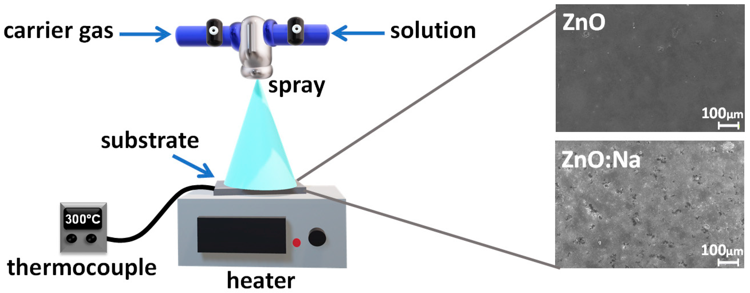
We analyzed undoped and sodium-doped zinc oxide thin films grown via the spray pyrolysis technique. The films were synthesized from two aqueous solutions: zinc acetate dihydrate (Zn(C2H3O2)2·2H2O), with a molar mass of 219.53 g/mol, and sodium hydroxide (NaOH), with a molar mass of 40.00 g/mol. By combining the solutions in proportions of 2, 4, 6, and 10% Na in the aqueous zinc acetate solution, we achieved different nominal dopant concentrations. The growth process involved deposition of the solutions onto a glass substrate preheated to 300 °C. The precursor solution was sprayed through an atomizing nozzle assisted by a carrier gas (0.1 MPa compressed air). Figure 1 illustrates a schematic of the spray pyrolysis setup employed for the growth of the films. SEM images indicated the uniformity of both the undoped ZnO and the 10% Na-doped film. The entire growth procedure was conducted while maintaining a flow rate of 0.3 mL/min. We labeled the ZnO:Na samples as follows: ZnO (0%Na), ZN2 (2%Na), ZN4 (4%Na), ZN6 (6%Na), and ZN10 (10%Na). In our defect engineering approach, we investigated the impact of annealing on the optical and electrical properties of an Na-doped ZnO film with 10% Na content concentration. The sample was divided into four parts. One part remained in its original state (as-grown), while the other three were annealed in atmospheres of argon (ZN10-Ar), nitrogen (ZN10-N2) and oxygen (ZN10-O2) at 500 °C for 1 h.
To assess the optical properties of the films, we conducted micro-photoluminescence (μPL) measurements using a 355 nm Cobolt Zouk laser with an output power of 15 mW as the excitation source. The μPL spectra were acquired within the temperature range of 10–300 K. The samples were kept within a Janis CCS-150 closed cryostat ) (Janis, Boston, MA, USA), and data acquisition was carried out using an Andor model iDus 420 CCD (Andor, Belfast, Ireland) connected to an Andor model Shamrock 500i spectrometer (Andor, Belfast, Ireland). To capture micrometric details, a precise LD EC Epiplan-Neofluar 50×/0.55 HD DIC M27 objective (Zeiss, Jena, Germany) was used to focus the laser on a small area of the film. The electrical characterization, including resistance (R) versus temperature (T) curves and Hall measurements, was carried out in a physical property measurement system (PPMS), model EverCool-II (Quantum Design, San Diego, CA, USA). This system operated within a closed liquid helium cycle, allowing it to work within the temperature range of 400 to 1.9 K. It featured a superconducting coil, enabling operation with magnetic fields of up to 9.0 T, and it also included an AC lock-in system. Temperature-dependent electrical resistance curves were measured within the range of 100–380 K, while Hall measurements were carried out in the range of 250–380 K. The magnetic field ranged from −2.0 T to 2.0 T, with a constant electric current of 1.10−5 mA applied. To investigate the crystalline quality of the samples based on the crystallite size of the films, we performed X-ray diffraction (XRD) measurements. These measurements utilized a diffractogram in Bragg–Brentano geometry with a Shimadzu model XRD-6100 diffractometer operating with a Cu-Kα radiation source (λ = 1.5406 Å). Additionally, the morphology of the films was examined using a scanning electron microscope (SEM), the JEOL JSM 6510 (JEOL, Tokyo, Japan), in secondary electron (SE) mode. Surface chemical analysis by X-ray photoelectron spectroscopy (XPS) was conducted utilizing a Thermo Scientific K-Alpha spectrometer (Thermo Fisher Scientific, Waltham, MA, USA) with monochromatic Al-Kα radiation (1486.6 eV). Binding energies were adjusted using adventitious carbon (C 1s–284.8 eV) as a standard reference.
3. Results and Discussions
3.1. Structural Characterization and Surface Chemical Analysis
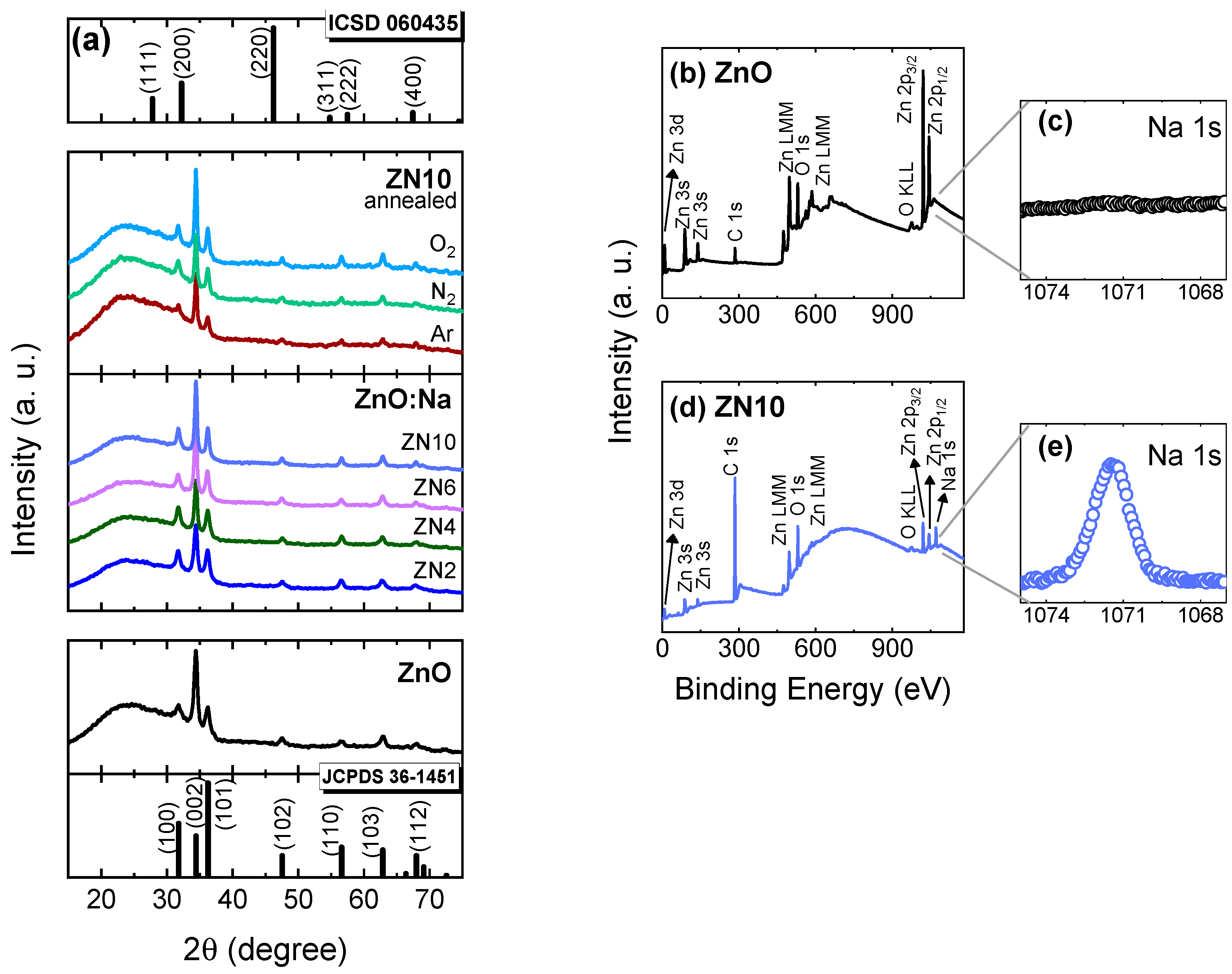
The ZnO and ZnO:Na films exhibited polycrystalline structures with a hexagonal wurtzite structure, as depicted in Figure 2a. Regardless of the addition of sodium, no secondary phase was detected within the equipment’s detection limit. Furthermore, a broad band centered at 2θ = 25° was observed due to the amorphous substrate. After annealing, the diffractograms exhibited a pattern similar to those of the as-grown films. Figure 2b,d show the survey scans of ZnO and ZnO:Na (10% Na content), respectively. The surface of the samples consisted of Zn, O, C, and Na (for the doped film), confirming the absence of contaminants on the surfaces of the samples. The high-resolution spectra in the Na 1s line, depicted in Figure 2c for ZnO and Figure 2e for ZN10, indicated the presence of the dopant in ZnO:Na. The binding energy of Na 1s was approximately 1071.4 eV.
3.2. Electrical Characterization
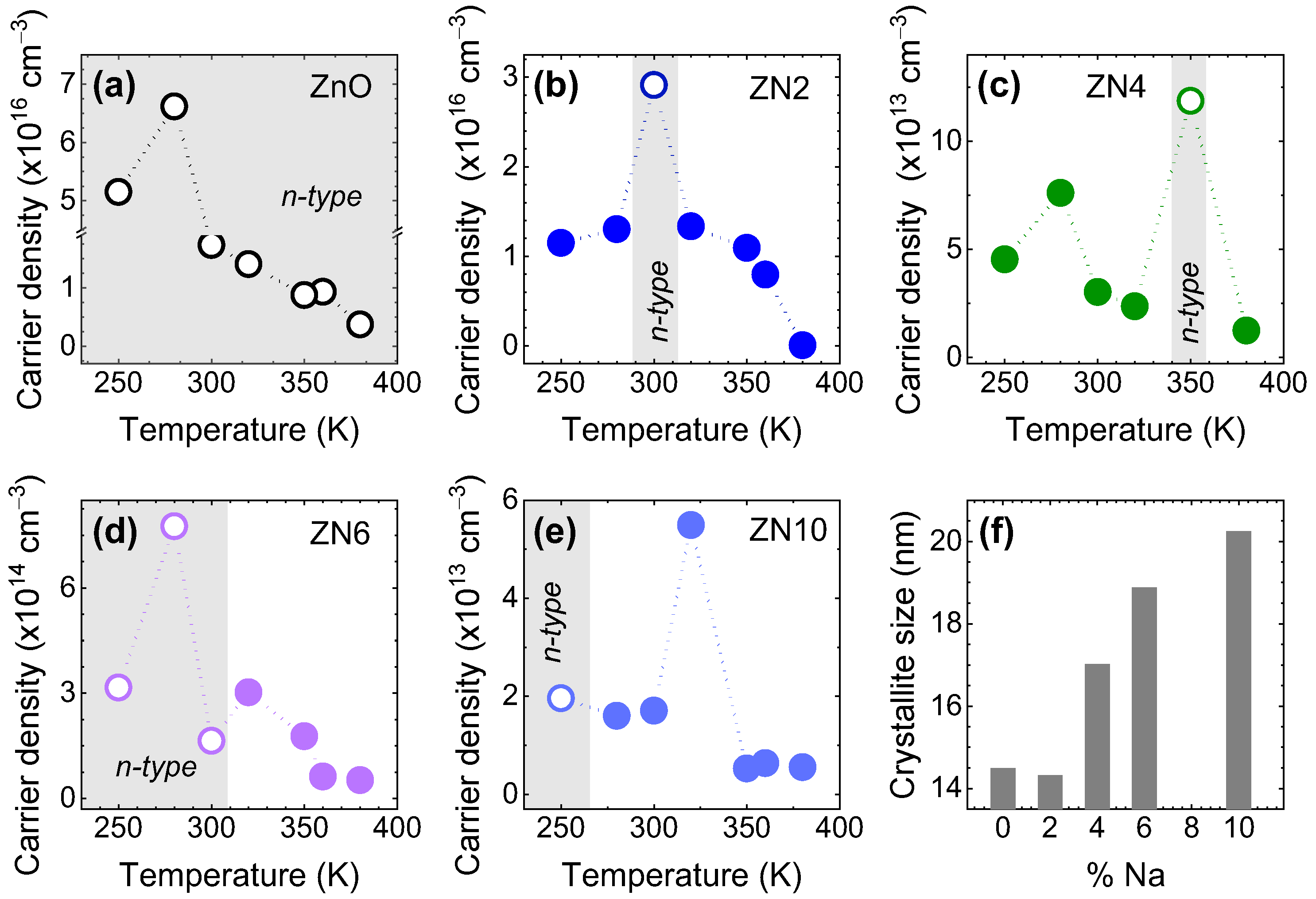
Figure 3 displays the temperature dependence of carrier density for ZnO and sodium-doped ZnO samples. The undoped ZnO film exhibited n-type conductivity, as observed in Figure 3a, with a carrier density in the order of 1016 cm−3. By incorporating sodium, the ZnO films doped at different concentrations, as shown in Figure 3b–e, illustrated that in specific temperature ranges, the dopant induced a change in the conductivity of the materials, making the transition from n-type to p-type. This phenomenon has also been observed in ZnO:Na nanorods and films grown using sol-gel [21,32]. However, the decrease in charge carriers was not noted as a general effect of Na-doping. The ZN10 sample showed a wider sequential temperature range, wherein the conductivity remained p-type (from 280 to 380 K). Furthermore, at this 10% Na dopant concentration, the film demonstrated the highest crystalline quality, as shown by the crystallite size in Figure 3f. The crystallite size was estimated using the Scherrer equation [33]. The undoped ZnO film showed a crystallite size of approximately 14.5 nm. Conversely, with 10% Na doping (ZN10), there was a 38% increase, resulting in a crystallite size of ~20 nm. Based on these findings, the ZN10 sample was also investigated after undergoing annealing in Ar, N2, and O2 atmospheres, as seen in Figure 4.
Focusing on the ZN10 sample, the annealing process resulted in an increase in carrier density (Figure 4). However, the employed treatment temperature and atmosphere conditions modified the conductivity type, acting as defect engineering. For the ZN10 film annealed in an inert atmosphere (Ar), the carrier density indicated an n-type conductivity (Figure 4a), while for ZN10 annealed in N2 and O2, as illustrated in Figure 4b, there was a narrowing of the temperature range where the semiconductor exhibited p-type behavior. It is important to highlight that ZN10 retained p-type characteristics within a room temperature window, with the carrier density being comparable to that of the undoped film. Figure 4c illustrates the crystallite size of the annealed ZN10. This result shows that annealing under different atmospheres preserved the crystalline quality of the samples, compared to the as-grown ZN10 (Figure 3f).
The characteristic curves of electrical resistance R versus 1/kBT, displayed in Figure 5, exhibit a semiconductor nature, as evidenced by the increase in electrical conductivity as the temperaturerises. By analyzing the profile of R as a function of temperature, we determined the thermal activation energies using Equation (1) [34]:
where R0 is the electrical resistance at T = 0 K, kB is the Boltzmann constant, and is the activation energy. The slopes of the linear regions observed in Figure 5 indicate the activation energy associated with impurities, defects, or traps in relation to the conduction or valence bands. In n-type samples, the activation energy represented the minimum energy required for electrons to be thermally promoted to the conduction band (CB), while for a p-type semiconductors, indicated the minimum energy for an electron in valence band (VB) to ascend to an acceptor level.
The as-grown films of ZnO, ZN2, and ZN10 were modeled considering three activation processes, as depicted in Figure 5a,b,e, respectively. Samples with 4 and 6% Na content exhibited two thermal activation channels, as illustrated in Figure 5c,d, respectively. Electrical activation energies are associated with the ionization of levels situated within the bandgap. As Na is incorporated, it can also trigger defects responsible for additional levels or compensating effects. It is notable that for both low (ZN2) and high (ZN10) sodium content samples, the electrical behavior displayed three activation channels contributing to p-type behavior. Nevertheless, the nature of these channels remains unknown. The highest values of were associated with high temperature regimes, while the lowest values were related to lower temperature regimes. The activation energy values are presented in Table 1. These activation energies ranged from tens to hundreds of meV. The lowest values of indicated shallow levels located near the bands (CB or VB), while the highest activation energies were associated to deep defect levels. Notably, samples ZN4 and ZN10 exhibited the highest values among the studied films. Figure 5f–h show the effect of ZN10 annealing in atmospheres of Ar, N2, and O2, respectively. The electrical resistance of these samples decreased compared to as-grown ZN10. Table 1 also features the thermal activation energies of annealed ZN10, as determined by Equation (1).
Contrasting the activation energies of the annealed and as-grown ZN10 films, annealing in different environments decreased and removed the deepest level (above one hundred meV). This outcome indicates that annealing mitigated the contribution of deep defects in the conductivity of Na-doped ZnO.
3.3. Optical Characterization
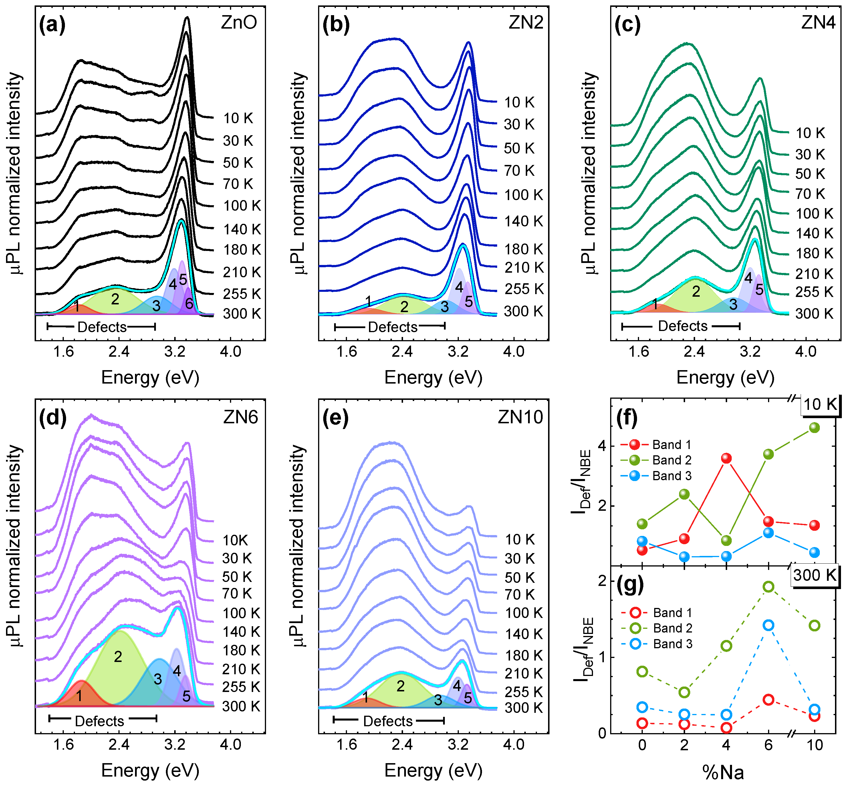
Figure 6a–e show the temperature dependence of the μPL emissions of the ZnO, ZN2, ZN4, ZN6, and ZN10 samples, respectively. The spectra displayed two main optical emission bands: one associated with crystalline defects in visible range between 1.40 and 2.95 eV, and another in the UV range from approximately 2.95 to 3.5 eV, which were attributed to band-to-band transitions (near to the absorption band edge, NBE) and excitonic complexes (~2.95–3.5 eV), respectively [35,36,37]. As seen in Figure 6a, it is evident that the emissions associated with NBE remained predominant in the ZnO films, regardless of temperature. Emissions similar to those of zinc oxide were observed for low sodium content samples, such as ZN2 and ZN4. NBE emissions exhibited greater intensity at near room temperature. However, as the temperature decreased, the defects emissions began to compete with NBE emissions. At concentrations above 6% Na, as shown in Figure 6d,e, the defects emissions became more pronounced in relation to emissions in the UV region. To analyze the emissions that overlapped and formed these broad bands, the curves were deconvoluted using Gaussian functions. It is worth noting that in the visible range, the three curves assigned as 1, 2, and 3 corresponded to the three primary colors red, green, and blue, respectively. In the violet and ultraviolet ranges, three Gaussian functions were fitted for ZnO (bands 4, 5, and 6), while sodium-doped films were fitted with two curves (bands 4 and 5). These bands were associated with NBE transitions, encompassing band-to-band transitions, free exciton (XA), and exciton bound to a neutral donor (D0X) [38,39,40].
The addition of Na dopant to the ZnO crystalline structure induced changes in the spectra profile, resulting in an increase in visible emissions compared to emissions close to the band edge. However, studies have reported that defects emissions in ZnO:Na nanostructures decrease in the presence of dopants [41,42,43]. This decrease has been attributed to enhanced electron-hole recombination, along with charge compensation effects due to native defects. Higher defects emissions were observed in the ZN6 and ZN10 films, as compared to the other films. Figure 6f,g show the relationship between the integrated intensity of the defect bands and the NBE (IDef/INBE) at 10 K and 300 K, respectively. Bands 1, 2, and 3 were identified in all spectra: band 1 exhibited an emission centered around 1.80 eV, band 2 of the undoped film showed an emission in the green centered at ~2.30 eV, while band 3 was centered at 2.90 eV. At both 10 K and 300 K, the green-centered emission was enhanced as Na concentration increased. Additionally, at lower temperatures, the emission in the red band became more prominent. Based on density functional theory (DFT), as presented in reference [36], the findings suggest that emission energies within the red/near infrared range (~1.8 eV) are correlated with zinc vacancies (VZN), while emissions around 2.2 or 2.3 eV (green-yellow emission) are associated with charged interstitial oxygens (Oi) and vacancy-related complexes (VZN or VO). According to these results, we inferred that the introduction of Na induced the formation of a higher concentration of defects, amplifying the green-yellow emission (2.30 eV) of the as-grown films.
The quenching of PL as a function of temperature was analyzed via the evaluation of integrated areas. Figure 7 shows the intensity of bands 1, 2, and 3 and NBE as a function of 1/kBT, which can be modeled using an Arrhenius-like expression for dual channel recombination, as in [44]:
where is the intensity at T = 0 K, is the activation energy of channel I associated to PL quenching, and is the correspondent ratio between radiative and non-radiative carrier lifetimes. A channel with large indicates the need for higher temperatures to activate a non-radiative process, i.e., to quench PL emission [44]. In Figure 7a, the NBE band exhibits two activation energies, 57 ± 3 meV and 13 ± 2 meV, which are attributed to the free exciton (XA) and the exciton bound to a neutral donor (D0X), respectively [38,39]. The excitonic energy found for the ZnO film was in accordance with the expected value of 60 meV. Similar temperature-dependent intensity patterns were observed for the defect band in zinc oxide and, considering the dual-channel approach, the activation energies were above the room temperature thermal energy of kBT ~26 meV. The optical activation energies of bands 1, 2, and 3, which were associated with red, green, and blue/violet emissions, respectively, are presented in Table 2.
The introduction of sodium into the ZnO crystal lattice leads to the formation of additional levels of defects in the semiconductor oxide bandgap. This suggests that different Na concentrations influenced emissions in the NBE region, promoting defect-related emissions in the visible region. Some of the activation energies related to PL quenching aligned with the approximate activation energies derived from electrical measurements (see Table 1). In such cases, carriers located within these levels can contribute to the electrical conductivity of the material. Although limited, some studies have suggested changes in the photoluminescence properties of sodium-doped ZnO films. In investigations concerning sol-gel-produced ZnO:Na thin films, the authors observed an emission peak at approximately 502 nm (2.46 eV). This emission was attenuated with the addition of sodium, attributed to the formation of complexes (Nazn − VO)+/0 [21,45]. In contrast, Na doping into ZnO nanorods, reported in [32], decreased the green emissions bound to Nai atoms. This reduction was attributed to sodium in zinc sites, which consequently suppressed oxygen vacancies. However, these results differed from those observed in our study. After annealing, we observed a redshift of the UV emissions, and an enhancement of red/near infrared emissions, as depicted in Figure 8a,b, at 10 K and 300 K. As previously discussed, the curves were fitted into four Gaussian function components.
The ratio between defects and NBE emissions, IDef/INBE, in Figure 8c,d, evidence an increase in green-yellow (2) and red/near infrared (1) emissions when annealing occurred in the inert and nitrogen atmospheres. The largest increases, around 1.75 eV and 2.2 eV, occurred for ZN10 annealed in a nitrogen atmosphere (at 10 K). Comparing these results with those of the as-grown ZN10 sample and with the theoretical study of ZnO [36], the increase in red/near infrared emissions can be attributed to Vzn-related defects. Although the optical characters of some defects emissions have been considered controversial, there has been some consensus that VZn is an acceptor type of defect [46,47]. In addition, annealing in oxidizing environment attenuates the emission around 2.2–2.3 eV (at 10 K), attributed to the charged Oi sites and vacancy complexes.
Figure 9 illustrates the integrated area intensity of each band depicted in Figure 8 as a function of 1/(kBT). The presence of Ar and N2 atmospheres during annealing impacted the emissions related to the UV region. However, when annealed in an oxidizing environment, its intensity decreased as temperature increased, and fitting was applied according to Equation (2). This same behavior was also observed for emissions corresponding to defects (band 1 and 2); band 1 (~1.75 eV) and band 2 (~2.2 eV) exhibited two activation energies for the ZN10-Ar and ZN10-N2 films, as seen in Figure 9a,b. The film treated in an O2 atmosphere showed only a single associated with the green-yellow emissions, which was similar to the as-grown ZN10 (~36 meV). The activation energy values associated with annealed ZN10 are presented in Table 2. Except for band 2 in ZN10-O2, shallow energy levels () were evident in all samples, with equivalent values. This suggests that the annealing atmosphere did not directly influence these levels, while samples thermally treated in Ar and N2 atmospheres exhibited higher values, associated with band 2, in relation to ZN10-O2.
Figure 10a illustrates a sketch of a band diagram, indicating the physical phenomena that govern the electrical and optical responses. Electrons in shallow donor levels can be thermally excited to the CB, while electrons in VB can be promoted to a shallow acceptor level. In addition, compensation mechanisms can act to trap the electrons from the acceptor level or the electrons from a donor level, which in both cases causes an increase in holes density. Concerning the optical response, photoexcited carriers undergo a thermalization process from the CB to VB via several channels, some associated to localized states, that can be optically active, resulting in the emission of light. It is worth noting the color of room temperature PL emissions due to excitation by UV light [48], as the spectra exhibited broad bands associated with RGB primary colors. Considering CIE (Commission Internationale De L’Eclairage) parameters, we evaluated the chromaticity coordinates x and y from the PL measurements [49], employing the GoCIE software [50] for CIE 1931 (Figure 10b). The emissions for as-grown samples were near the white even in pure ZnO, but the introduction of Na induced a bluish (cold) white light, except for in the sample with 10% Na content. While as-grown ZN10 presented a near neutral white color, annealing ran to a warm white, with O2 annealing resulting in a red trend [51].
4. Conclusions
Na doping in the ZnO crystal structure induces a switching from n-type to p-type conductivities in specific temperature ranges. However, charge compensation mechanisms diminish the majority carrier density, which is enhanced after annealing in controlled atmospheres. A correlation between sodium content and defects emissions in PL measurements is observed, with the green- yellow emissions being the most pronounced for as-grown doped samples. These emissions suggest that the levels created by Na are responsible for capturing electrons from inherent levels of ZnO and, consequently, promoting p-type conductivity and carrier density decrease. The annealing procedure induces a notable enhancement in red/infrared emissions for 10% Na content samples. Annealing in N2 or O2 atmospheres also allows a room temperature window in which the conductivity remains p-type.
Author Contributions
Conceptualization, A.L.C.S. and M.P.F.d.G.; methodology, A.L.C.S., M.P.F.d.G., L.M.B.V., M.L.P. and M.D.T.; validation, A.L.C.S., M.P.F.d.G., M.L.P. and M.D.T.; formal analysis, A.L.C.S., M.P.F.d.G., L.M.B.V. and M.L.P.; investigation, A.L.C.S., M.P.F.d.G., L.M.B.V., M.L.P. and M.D.T.; resources, M.P.F.d.G., M.L.P. and M.D.T.; data curation, A.L.C.S., M.P.F.d.G., L.M.B.V. and M.L.P.; writing—original draft preparation, A.L.C.S. and M.P.F.d.G.; writing—review and editing, A.L.C.S., M.P.F.d.G., L.M.B.V., M.L.P. and M.D.T.; supervision, M.P.F.d.G.; project administration, M.P.F.d.G.; funding acquisition, M.P.F.d.G., M.L.P. and M.D.T. All authors have read and agreed to the published version of the manuscript.
Funding
This work was supported by the Conselho Nacional de Desenvolvimento Científico e Tecnológico—CNPq (grant number 312254/2023-7), Coordenação de Aperfeiçoamento de Pessoal de Nível Superior—CAPES and Fundação de Amparo à Pesquisa do Estado de São Paulo—FAPESP (grant number 2022/10340-2).
Institutional Review Board Statement
Not applicable.
Informed Consent Statement
Not applicable.
Data Availability Statement
Data could be available given the appropriate request.
Acknowledgments
We gratefully acknowledge the resources provided by the Brazilian Nanotechnology National Laboratory (LNNano), which operates under the Brazilian Centre for Research in Energy and Materials (CNPEM), a private non-profit organization overseen by the Brazilian Ministry for Science, Technology, and Innovations (MCTI). We appreciate the support provided by the XPS team for their assistance during the experiments (proposals XPS-28104 and XPS-28108). We also thank Adenilson José Chiquito for the SEM measurements and Aline Bastos de Paiva for her assistance in the micro-PL measurements. In addition, technical support from Natalia Zanardi and Roberto Sabadini is gratefully recognized. M.P.F.d.G. thanks the support of CNPq grant 312254/2023-7. M.D.T. thanks the support of FAPESP grant 2022/10340-2. A.L.C.S. and L.M.B.V. acknowledge the support of their doctorate fellowships from CAPES.
Conflicts of Interest
The authors declare no conflicts of interest.
References
- Dimitrov, D.; Tsai, C.L.; Petrov, S.; Marinova, V.; Petrova, D.; Napoleonov, B.; Blagoev, B.; Strijkova, V.; Hsu, K.Y.; Lin, S.H. Atomic Layer-Deposited Al-Doped ZnO Thin Films for Display Applications. Coatings 2020, 10, 539. [Google Scholar] [CrossRef]
- Meng, L.; Yang, X.; Chai, H.; Lv, Z.; Yang, T. Surface Modification of Al-Doped ZnO Transparent Conducive Thin Films with Polycrystalline Zinc Molybdenum Oxide. ACS Appl. Mater. Interfaces 2019, 11, 26491–26499. [Google Scholar] [CrossRef] [PubMed]
- Jang, J.; Kang, Y.; Cha, D.; Bae, J.; Lee, S. Thin-Film Optical Devices Based on Transparent Conducting Oxides: Physical Mechanisms and Applications. Crystals 2019, 9, 192. [Google Scholar] [CrossRef]
- Kevin, M.; Tho, W.H.; Ho, G.W. Transferability of Solution Processed Epitaxial Ga:ZnO Films; Tailored for Gas Sensor and Transparent Conducting Oxide Applications. J. Mater. Chem. 2012, 22, 16442–16447. [Google Scholar] [CrossRef]
- Imran, A.; Zhu, Q.; Sulaman, M.; Bukhtiar, A.; Xu, M. Electric-Dipole Gated Two Terminal Phototransistor for Charge-Coupled Device. Adv. Opt. Mater. 2023, 11, 2300910. [Google Scholar] [CrossRef]
- Minami, T. Present Status of Transparent Conducting Oxide Thin-Film Development for Indium-Tin-Oxide (ITO) Substitutes. Thin Solid Film. 2008, 516, 5822–5828. [Google Scholar] [CrossRef]
- Cole-Hamilton, D.J. Elements of Scarcity. Chem. Int. 2019, 41, 23–28. [Google Scholar] [CrossRef]
- Ramos, R.; Chaves, M.; Martins, E.; Durrant, S.F.; Rangel, E.C.; Da Silva, T.F.; Bortoleto, J.R.R. Growth Evolution of AZO Thin Films Deposited by Magnetron Sputtering at Room Temperature. Mater. Res. 2021, 24, e20210052. [Google Scholar] [CrossRef]
- Laurenti, M.; Cauda, V. Porous Zinc Oxide Thin Films: Synthesis Approaches and Applications. Coatings 2018, 8, 67. [Google Scholar] [CrossRef]
- Ponja, S.D.; Sathasivam, S.; Parkin, I.P.; Carmalt, C.J. Highly Conductive and Transparent Gallium Doped Zinc Oxide Thin Films via Chemical Vapor Deposition. Sci. Rep. 2020, 10, 638. [Google Scholar] [CrossRef]
- Koralli, P.; Varol, S.F.; Mousdis, G.; Mouzakis, D.E.; Merdan, Z.; Kompitsas, M. Comparative Studies of Undoped/Al-Doped/In-Doped ZnO Transparent Conducting Oxide Thin Films in Optoelectronic Applications. Chemosensors 2022, 10, 162. [Google Scholar] [CrossRef]
- Kraut, M.; Sirotti, E.; Pantle, F.; Jiang, C.M.; Grötzner, G.; Koch, M.; Wagner, L.I.; Sharp, I.D.; Stutzmann, M. Control of Band Gap and Band Edge Positions in Gallium-Zinc Oxynitride Grown by Molecular Beam Epitaxy. J. Phys. Chem. C 2020, 124, 7668–7676. [Google Scholar] [CrossRef]
- Zhao, D.; Li, J.; Sathasivam, S.; Carmalt, C.J. N-Type Conducting P Doped ZnO Thin Films via Chemical Vapor Deposition. RSC Adv. 2020, 10, 34527–34533. [Google Scholar] [CrossRef] [PubMed]
- Sze, S.M.; Ng, K.K. Physics of Semiconductor Devices, 3rd ed.; Wiley-Interscience: New York, NY, USA, 2006. [Google Scholar]
- Lin, S.S.; Lu, J.G.; Ye, Z.Z.; He, H.P.; Gu, X.Q.; Chen, L.X.; Huang, J.Y.; Zhao, B.H. P-Type Behavior in Na-Doped ZnO Films and ZnO Homojunction Light-Emitting Diodes. Solid State Commun. 2008, 148, 25–28. [Google Scholar] [CrossRef]
- Mukai, K.N.; Bernardes, J.C.; Müller, D.; Rambo, C.R. Rectifying ZnO–Na/ZnO–Al Aerogels p-n Homojunctions. J. Mater. Sci. Mater. Electron. 2022, 33, 7738–7749. [Google Scholar] [CrossRef] [PubMed]
- Kwon, D.K.; Porte, Y.; Myoung, J.M. Fabrication of ZnO Nanorods P-n Homojunction Light-Emitting Diodes Using Ag Film as Self-Doping Source for p-Type ZnO Nanorods. J. Phys. Chem. C 2018, 122, 11993–12001. [Google Scholar] [CrossRef]
- Rahman, M.; Kamruzzaman, M.; Zapien, J.A.; Afrose, R.; Anam, T.K.; Liton, M.N.H.; Helal, M.A.; Khan, M.K.R. Conversion of N-Type to p-Type Conductivity in ZnO by Incorporation of Ag and Ag-Li. Mater. Today Commun. 2022, 33, 104278. [Google Scholar] [CrossRef]
- Snigurenko, D.; Kopalko, K.; Krajewski, T.A.; Jakiela, R.; Guziewicz, E. Nitrogen Doped P-Type ZnO Films and p-n Homojunction. Semicond. Sci. Technol. 2014, 30, 015001. [Google Scholar] [CrossRef]
- Li, X.; Yan, Y.; Gessert, T.A.; Perkins, C.L.; Young, D.; Dehart, C.; Young, M.; Coutts, T.J.; Yan, Y.; Young, D.; et al. Chemical Vapor Deposition-Formed p-Type ZnO Thin Films. J. Vac. Sci. Technol. A 2003, 21, 1342–1346. [Google Scholar] [CrossRef]
- Erdogan, N.H.; Kutlu, T.; Sedefoglu, N.; Kavak, H. Effect of Na Doping on Microstructures, Optical and Electrical Properties of ZnO Thin Films Grown by Sol-Gel Method. J. Alloys Compd. 2021, 881, 160554. [Google Scholar] [CrossRef]
- Zagal-Padilla, C.K.; García-Sandoval, J.; Gamboa, S.A. A Feasible and Low-Cost Green Route to Prepare ZnO with n or p-Type Conductivity by Changing the Parsley Extract Concentration. J. Alloys Compd. 2022, 891, 162087. [Google Scholar] [CrossRef]
- Swapna, R.; Santhosh Kumar, M.C. Deposition of Na–N Dual Acceptor Doped p-Type ZnO Thin Films and Fabrication of p-ZnO:(Na, N)/n-ZnO:Eu Homojunction. Mater. Sci. Eng. B 2013, 178, 1032–1039. [Google Scholar] [CrossRef]
- Yuan, G.D.; Ye, Z.Z.; Zhu, L.P.; Qian, Q.; Zhao, B.H.; Fan, R.X.; Perkins, C.L.; Zhang, S.B. Control of Conduction Type in Al- and N-Codoped ZnO Thin Films. Appl. Phys. Lett. 2005, 86, 202106. [Google Scholar] [CrossRef]
- Nripasree, N.; Deepak, N.K. Structural, Optical and Electrical Properties of SnN Codoped p Type ZnO Thin Films Prepared by Spray Pyrolysis Technique for Diode Applications. Mater. Sci. Eng. B 2016, 211, 121–127. [Google Scholar] [CrossRef]
- Zhao, Y.; Yang, H.; Xiao, Y.; Yang, P. A Pathway for ZnO P-Type Transformation and Its Performance in Solar Cells. Sol. Energy 2022, 231, 889–896. [Google Scholar] [CrossRef]
- Kampylafka, V.; Kostopoulos, A.; Modreanu, M.; Schmidt, M.; Gagaoudakis, E.; Tsagaraki, K.; Kontomitrou, V.; Konstantinidis, G.; Deligeorgis, G.; Kiriakidis, G.; et al. Long-Term Stability of Transparent n/p ZnO Homojunctions Grown by Rf-Sputtering at Room-Temperature. J. Mater. 2019, 5, 428–435. [Google Scholar] [CrossRef]
- Park, C.H.; Zhang, S.B.; Wei, S.H. Origin of P-Type Doping Difficulty in ZnO: The Impurity Perspective. Phys. Rev. B 2002, 66, 073202. [Google Scholar] [CrossRef]
- Jannane, T.; Manoua, M.; Fazouan, N.; El Hichou, A.; Almaggoussi, A.; Liba, A. Self-Compensation Reduction as First Step of p-Type ZnO Synthesis. Superlattices Microstruct. 2020, 147, 106689. [Google Scholar] [CrossRef]
- Jacobsson, T.J.; Viarbitskaya, S.; Mukhtar, E.; Edvinsson, T. A Size Dependent Discontinuous Decay Rate for the Exciton Emission in ZnO Quantum Dots. Phys. Chem. Chem. Phys. 2014, 16, 13849–13857. [Google Scholar] [CrossRef] [PubMed]
- Tarasov, A.P.; Ismailov, A.M.; Gadzhiev, M.K.; Venevtsev, I.D.; Muslimov, A.E.; Volchkov, I.S.; Aidamirova, S.R.; Tyuftyaev, A.S.; Butashin, A.V.; Kanevsky, V.M. Effect of Plasma Treatment on the Luminescent and Scintillation Properties of Thick ZnO Films Fabricated by Sputtering of a Hot Ceramic Target. Photonics 2023, 10, 1354. [Google Scholar] [CrossRef]
- Ye, Z.; Wang, T.; Wu, S.; Ji, X.; Zhang, Q. Na-Doped ZnO Nanorods Fabricated by Chemical Vapor Deposition and Their Optoelectrical Properties. J. Alloys Compd. 2017, 690, 189–194. [Google Scholar] [CrossRef]
- Cullity, B.D. Elements of X-ray Diffraction; Addison-Wesley Publishing: Reading, MA, USA, 1956; p. 514. [Google Scholar]
- McCluskey, M.D.; Haller, E.E. Dopants and Defects in Semiconductors; CRC Press: Boca Raton, FL, USA; Taylor & Francis: New York, NY, USA, 2012; ISBN 1439831521. [Google Scholar]
- Deekshitha, U.G.; Upadhya, K.; Antony, A.; Ani, A.; Nowak, M.; Kityk, I.V.; Jedryka, J.; Poornesh, P.; Manjunatha, K.B.; Kulkarni, S.D. Effect of Na Doping on Photoluminescence and Laser Stimulated Nonlinear Optical Features of ZnO Nanostructures. Mater. Sci. Semicond. Process. 2019, 101, 139–148. [Google Scholar] [CrossRef]
- Cabral, L.; Lopez-Richard, V.; Da Silva, J.L.F.; Marques, G.E.; Lima, M.P.; Onofre, Y.J.; Teodoro, M.D.; de Godoy, M.P.F. Insights into the Nature of Optically Active Defects of ZnO. J. Lumin. 2020, 227, 117536. [Google Scholar] [CrossRef]
- Klingshirn, C.F.; Meyer, B.K.; Waag, A.; Hoffmann, A.; Geurts, J. Zinc Oxide; Springer: Berlin/Heidelberg, Germany, 2010; Volume 120. [Google Scholar] [CrossRef]
- Teke, A.; Özgür, Ü.; Doǧan, S.; Gu, X.; Morkoç, H.; Nemeth, B.; Nause, J.; Everitt, H.O. Excitonic Fine Structure and Recombination Dynamics in Single-Crystalline ZnO. Phys. Rev. B 2004, 70, 195207. [Google Scholar] [CrossRef]
- Meyer, B.K.; Sann, J.; Lautenschläger, S.; Wagner, M.R.; Hoffmann, A. Ionized and Neutral Donor-Bound Excitons in ZnO. Phys. Rev. B 2007, 76, 184120. [Google Scholar] [CrossRef]
- Loan, T.T.; Long, N.N.; Ha, L.H. Photoluminescence Properties of Co-Doped ZnO Nanorods Synthesized by Hydrothermal Method. J. Phys. D Appl. Phys. 2009, 42, 065412. [Google Scholar] [CrossRef]
- Hassanpour, A.; Shen, S.; Bianucci, P. Sodium-Doped Oriented Zinc Oxide Nanorod Arrays: Insights into Their Aqueous Growth Design, Crystal Structure, and Optical Properties. MRS Commun. 2018, 8, 570–576. [Google Scholar] [CrossRef]
- Elsayed, M.H.; Elmorsi, T.M.; Abuelela, A.M.; Hassan, A.E.; Alhakemy, A.Z.; Bakr, M.F.; Chou, H.H. Direct Sunlight-Active Na-Doped ZnO Photocatalyst for the Mineralization of Organic Pollutants at Different PH Mediums. J. Taiwan Inst. Chem. Eng. 2020, 115, 187–197. [Google Scholar] [CrossRef]
- Straube, B.; Bridoux, G.; Zapata, C.; Ferreyra, J.M.; Villafuerte, M.; Simonelli, G.; Esquinazi, P.; Rodríguez Torres, C.; Perez de Heluani, S.I. Effect of Doping and Morphology on UV Emission in Low-Dimensional ZnO:Na Structures. Phys. Status Solidi (b) 2018, 255, 1800056. [Google Scholar] [CrossRef]
- Correr, G.I.; Badillo, F.A.L.; Botero, E.R.; Milton, F.P.; Garcia, D.; de Godoy, M.P.F. Nd3+ Emissions in Transparent Ferroelectric Ceramic Hosts under Ultraviolet Excitation. Ceram. Int. 2022, 48, 13331–13339. [Google Scholar] [CrossRef]
- Wang, L.W.; Wu, F.; Tian, D.X.; Li, W.J.; Fang, L.; Kong, C.Y.; Zhou, M. Effects of Na Content on Structural and Optical Properties of Na-Doped ZnO Thin Films Prepared by Sol–Gel Method. J. Alloys Compd. 2015, 623, 367–373. [Google Scholar] [CrossRef]
- Leung, Y.H.; Chen, X.Y.; Ng, A.M.C.; Guo, M.Y.; Liu, F.Z.; Djurišić, A.B.; Chan, W.K.; Shi, X.Q.; Van Hove, M.A. Green Emission in ZnO Nanostructures—Examination of the Roles of Oxygen and Zinc Vacancies. Appl. Surf. Sci. 2013, 271, 202–209. [Google Scholar] [CrossRef]
- Janotti, A.; Van De Walle, C.G. Native Point Defects in ZnO. Phys. Rev. B 2007, 76, 165202. [Google Scholar] [CrossRef]
- Ji, J.; Colosimo, A.M.; Anwand, W.; Boatner, L.A.; Wagner, A.; Stepanov, P.S.; Trinh, T.T.; Liedke, M.O.; Krause-Rehberg, R.; Cowan, T.E.; et al. ZnO Luminescence and Scintillation Studied via Photoexcitation, X-ray Excitation and Gamma-Induced Positron Spectroscopy. Sci. Rep. 2016, 6, 31238. [Google Scholar] [CrossRef]
- Huang, B.; Yang, H.; Zhang, L.; Yuan, Y.; Cui, Y.; Zhang, J. Effect of Surface/Interfacial Defects on Photo-Stability of Thick-Shell CdZnSeS/ZnS Quantum Dots. Nanoscale 2018, 10, 18331–18340. [Google Scholar] [CrossRef]
- Justin Thomas, K.R.; Department of Chemistry, Indian Institute of Technology Roorkee, India. 2009. Available online: https://faculty.iitr.ac.in/~krjt8fcy/gocie.html (accessed on 28 February 2024).
- Thapa, S.; Adhikari, G.C.; Zhu, P.; Zhu, H. Spectral Optimization of White Light from Hybrid Metal Halide Perovskites. OSA Contin. 2019, 2, 1880–1888. [Google Scholar] [CrossRef]
Figure 1.
Spray pyrolysis configuration used for the growth of ZnO and ZnO:Na films. The SEM images indicate the uniformity of the films at a 100 μm scale.
Figure 1.
Spray pyrolysis configuration used for the growth of ZnO and ZnO:Na films. The SEM images indicate the uniformity of the films at a 100 μm scale.

Figure 2.
(a) Diffractograms of the ZnO, as-grown ZnO:Na, and ZN10 annealed samples. ICSD 060435 and JCPDS 36-1451 are crystallographic standards for sodium and zinc oxides, respectively. XPS survey scans of as-grown ZnO (b) and ZN10 (d) with Na 1s high-resolution spectra for ZnO (c) and ZN10 (e).
Figure 2.
(a) Diffractograms of the ZnO, as-grown ZnO:Na, and ZN10 annealed samples. ICSD 060435 and JCPDS 36-1451 are crystallographic standards for sodium and zinc oxides, respectively. XPS survey scans of as-grown ZnO (b) and ZN10 (d) with Na 1s high-resolution spectra for ZnO (c) and ZN10 (e).

Figure 3.
Carrier density of as-grown ZnO (a) and sodium-doped ZnO (b–e) films ZN2, ZN4, ZN6, and ZN10, respectively. Open dots represent n-type conductivity (gray area), while filled dots indicate p-type conductivity. Additionally, (f) shows the bar chart with the crystallite size of the samples.
Figure 3.
Carrier density of as-grown ZnO (a) and sodium-doped ZnO (b–e) films ZN2, ZN4, ZN6, and ZN10, respectively. Open dots represent n-type conductivity (gray area), while filled dots indicate p-type conductivity. Additionally, (f) shows the bar chart with the crystallite size of the samples.

Figure 4.
Carrier density of the ZN10 annealed in (a) Ar and (b) N2 and O2 atmospheres. The gray area indicates that the conductivity is n-type (empty dots). The filled dots indicate that the conductivity is p-type. (c) Crystallite size of ZN10-Ar, ZN10-N2, and ZN10-O2 films.
Figure 4.
Carrier density of the ZN10 annealed in (a) Ar and (b) N2 and O2 atmospheres. The gray area indicates that the conductivity is n-type (empty dots). The filled dots indicate that the conductivity is p-type. (c) Crystallite size of ZN10-Ar, ZN10-N2, and ZN10-O2 films.

Figure 5.
Characteristic curves of electrical resistance versus temperature of as-grown samples of (a) ZnO, (b) ZN2, (c) ZN4, (d) ZN6, and (e) ZN10. ZN10 films annealed in an atmosphere of (f) Ar, (g) N2, and (h) O2. The solid red line indicates the fitting curves.
Figure 5.
Characteristic curves of electrical resistance versus temperature of as-grown samples of (a) ZnO, (b) ZN2, (c) ZN4, (d) ZN6, and (e) ZN10. ZN10 films annealed in an atmosphere of (f) Ar, (g) N2, and (h) O2. The solid red line indicates the fitting curves.

Figure 6.
The temperature dependence of μPL spectra of undoped ZnO film (a) and Na-doped ZnO films: (b) ZN2, (c) ZN4, (d) ZN6, and (e) ZN10. The ratios between the integrated intensity of defect bands 1, 2, and 3 and the NBE (IDef/INBE) at 10K (f) and 300 K (g) are also displayed.
Figure 6.
The temperature dependence of μPL spectra of undoped ZnO film (a) and Na-doped ZnO films: (b) ZN2, (c) ZN4, (d) ZN6, and (e) ZN10. The ratios between the integrated intensity of defect bands 1, 2, and 3 and the NBE (IDef/INBE) at 10K (f) and 300 K (g) are also displayed.

Figure 7.
Integrated μPL intensity as a function of 1/kBT for the bands associated with the defects (band 1, band 2, and band 3) and the band related to the emission of energy in the UV range of the ZnO film (a) and the sodium-doped samples: (b) ZN2, (c) ZN4, (d) ZN6, and (e) ZN10. The solid red line indicates the fitting curves.

Figure 8.
μPL spectra of as-grown and annealed ZN10 film in Ar, N2, and O2 atmospheres at (a) 10 K and (b) 300 K. Additionally, the ratio between the integrated intensity of defect bands 1, 2, and 3 and the NBE (IDef/INBE) at 10K (c) and 300 K (d) is also shown – Band 4 is associated with the NBE.
Figure 8.
μPL spectra of as-grown and annealed ZN10 film in Ar, N2, and O2 atmospheres at (a) 10 K and (b) 300 K. Additionally, the ratio between the integrated intensity of defect bands 1, 2, and 3 and the NBE (IDef/INBE) at 10K (c) and 300 K (d) is also shown – Band 4 is associated with the NBE.

Figure 9.
Integrated intensity of μPL versus 1/kBT for the bands associated with the defects (band 1 and band 2) and the band related to the emissions in the UV energy region of the ZN10 annealed in (a) argon (ZN10-Ar); (b) nitrogen (ZN10-N2) and (c) oxygen (ZN10-O2). The solid red line indicates the fitting curves.

Figure 10.
(a) Sketch of energy band diagram elucidating electrical and optical processes. (b) Room temperature PL emissions of samples depicted in the CIE 1931 diagram exhibited a white pattern. The annealing caused a redshift of emissions due to the increase in defects.
Figure 10.
(a) Sketch of energy band diagram elucidating electrical and optical processes. (b) Room temperature PL emissions of samples depicted in the CIE 1931 diagram exhibited a white pattern. The annealing caused a redshift of emissions due to the increase in defects.


Table 1.
Activation energies () of as-grown ZnO and ZnO:Na films, as well as annealed ZN10, determined from R × 1/kBT curves.
Table 1.
Activation energies () of as-grown ZnO and ZnO:Na films, as well as annealed ZN10, determined from R × 1/kBT curves.
| Samples | (meV) | (meV) | (meV) |
|---|---|---|---|
| ZnO | 23.0 ± 1.0 | 12.0 ± 0.5 | 6.0 ± 0.2 |
| ZN2 | 21.5 ± 1.0 | 13.5 ± 0.5 | 10.0 ± 0.5 |
| ZN4 | 147 ± 18 | 53.0 ± 1.5 | |
| ZN6 | 27.0 ± 1.0 | 9.0 ± 0.5 | |
| ZN10 | 198 ± 24 | 40.0 ± 1.0 | 11.0 ± 0.5 |
| ZN10-Ar | 21.0 ± 1.0 | 10.0 ± 0.5 | |
| ZN10-N2 | 14.5 ± 0.5 | 4.5 ± 0.1 | 3.5 ± 0.1 |
| ZN10-O2 | 21.0 ± 1.0 | 10.0 ± 0.5 | 5.0 ± 0.1 |
Table 2.
Optical activation energies () of ZnO, as-grown ZnO:Na, and annealed ZN10.
| Samples | NBE | Defects | ||||||
|---|---|---|---|---|---|---|---|---|
| Band 1 | Band 2 | Band 3 | ||||||
| (meV) | (meV) | (meV) | (meV) | (meV) | (meV) | (meV) | (meV) | |
| ZnO | 57 ± 3 | 13 ± 2 | 51 ± 3 | 10 ± 1 | 49 ± 3 | 5 ± 1 | 50 ± 6 | 7 ± 1 |
| ZN2 | 51 ± 3 | 9 ± 1 | 46 ± 3 | 8 ± 1 | ||||
| ZN4 | 53 ± 3 | 15 ± 3 | 46 ± 3 | |||||
| ZN6 | 19 ± 3 | 14 ± 4 | ||||||
| ZN10 | 46 ± 4 | 36 ± 2 | ||||||
| ZN10-Ar | 44 ± 3 | 7 ± 2 | 45 ± 2 | 10 ± 1 | ||||
| ZN10-N2 | 48 ± 2 | 10 ± 1 | 53 ± 1 | 8 ± 1 | ||||
| ZN10-O2 | 43 ± 3 | 12 ± 2 | 52 ± 1 | 7 ± 1 | 36 ± 1 | |||
Disclaimer/Publisher’s Note: The statements, opinions and data contained in all publications are solely those of the individual author(s) and contributor(s) and not of MDPI and/or the editor(s). MDPI and/or the editor(s) disclaim responsibility for any injury to people or property resulting from any ideas, methods, instructions or products referred to in the content. |
© 2024 by the authors. Licensee MDPI, Basel, Switzerland. This article is an open access article distributed under the terms and conditions of the Creative Commons Attribution (CC BY) license (https://creativecommons.org/licenses/by/4.0/).
Share and Cite
MDPI and ACS Style
Silva, A.L.C.; Vargas, L.M.B.; Peres, M.L.; Teodoro, M.D.; de Godoy, M.P.F. Exploring Na Doping in ZnO Thin Films: Electrical and Optical Insights. Coatings 2024, 14, 510. https://doi.org/10.3390/coatings14040510
AMA Style
Silva ALC, Vargas LMB, Peres ML, Teodoro MD, de Godoy MPF. Exploring Na Doping in ZnO Thin Films: Electrical and Optical Insights. Coatings. 2024; 14(4):510. https://doi.org/10.3390/coatings14040510
Chicago/Turabian StyleSilva, Ana Luiza C., Luis M. B. Vargas, Marcelos L. Peres, Marcio D. Teodoro, and Marcio P. F. de Godoy. 2024. "Exploring Na Doping in ZnO Thin Films: Electrical and Optical Insights" Coatings 14, no. 4: 510. https://doi.org/10.3390/coatings14040510
Note that from the first issue of 2016, this journal uses article numbers instead of page numbers. See further details here.