Article

Effect of Annealing on Stress, Microstructure, and Interfaces of NiV/B4C Multilayers

1
Key Laboratory of Advanced Micro-Structured Materials, MOE, Institute of Precision Optical Engineering, School of Physics Science and Engineering, Tongji University, Shanghai 200092, China
2
Shanghai Synchrotron Radiation Facility, Shanghai Advanced Research Institute, Chinese Academy of Sciences, 239 Zhangheng Road, Pudong District, Shanghai 201204, China
*
Authors to whom correspondence should be addressed.
These authors contributed equally to this work.
Coatings 2024, 14(4), 513; https://doi.org/10.3390/coatings14040513
Submission received: 28 March 2024 / Revised: 18 April 2024 / Accepted: 19 April 2024 / Published: 20 April 2024
(This article belongs to the Special Issue Thin-Film Synthesis, Characterization and Properties)

Abstract

:
The functionality and reliability of nanoscale multilayer devices and components are influenced by changes in stress and microstructure throughout fabrication, processing, and operation. NiV/B4C multilayers with a d-spacing of 3 nm were prepared by magnetron sputtering, and two groups of annealing experiments were performed. The stress, microstructure, and interface changes in NiV/B4C after annealing were investigated by grazing-incidence X-ray reflectometry (GIXR), grazing-incidence X-ray diffraction (GIXRD), X-ray diffuse scattering, and grazing-incidence small-angle X-ray scattering (GISAXS). The temperature dependence experiments revealed a gradual shift in the multilayer stress from compression to tension during annealing from 70 °C to 340 °C, with the stress approaching near-zero levels between 70 °C and 140 °C. The time-dependent experiments indicated that most of the stress changes occurred within the initial 10 min, which showed that prolonged annealing was unnecessary. Combining the X-ray diffraction and X-ray scattering measurements, it was found that the changes in the thickness, interface roughness, and lateral correlation length, primarily due to crystallization, drove the changes in stress and microstructure.

1. Introduction

Nanoscale multilayers are nanometer-thick films of different alternating materials stacked periodically on each other. The nanoscale multilayers have extensive applications in advanced imaging, spectroscopy, and monochromator systems in synchrotron radiation [1,2,3,4,5,6]. Short-period multilayer films are becoming increasingly required for monochromators of synchrotron radiation to meet the conditions of a large grazing-incidence angle, higher working energy, and higher energy resolution. Owing to the fact that NiV has no absorption line in the light energy range of 20 to 200 keV, and considering its higher reflectivity and integral flux, the NiV/B4C combination is an excellent material for monochromators [7,8,9,10]. The optical properties and stability of multilayer monochromators are affected and their service life is reduced due to the accumulated stress and interface defects that occur during deposition [11,12,13,14]. As one of the primary optical elements in a synchrotron radiation beamline, the multilayer monochromators are subjected to an exceptionally high photon flux and heat load. This exposure can lead to the degradation of the nanoscale multilayer structure. Hence, it is imperative for the multilayer to possess excellent thermal stability to guarantee long-term reliability in synchrotron radiation monochromators.
The annealing process is a common method used to study the thermal stability of multilayers. Numerous experimental studies have investigated stress and related microstructural changes that occur during annealing in various small-period multilayers. For instance, Nguyen et al. fabricated Ru/C multilayers with periods of 2 nm, 5 nm, and 10 nm and annealed them at 500 °C. They found that the period increased after annealing. Crystallization occurred after annealing the multilayer films with periodic thicknesses of 5.0 nm and 10.0 nm [15]. Nguyen et al. also explored the thermal stability of Ru/C and Ru/B4C multilayers with a periodic thickness of d = 3.5 nm when subjected to annealing at 600 °C. Following annealing at 600 °C, both multilayers exhibited periodic expansion of the Ru layer. This expansion contributed to an increase in the interface roughness due to crystallization [16]. Geisz et al. fabricated W/C multilayers with a periodic thickness of 4 nm and annealed them within the range of 400–500 °C. The results revealed a slight expansion of the multilayer film post annealing; the grain growth promotes stress relaxation [17]. Barthelmess et al. developed a Mo/B4C multilayer film with a thickness of 3.5 nm and annealed it across temperatures ranging from 100 to 900 °C. The results indicated a membrane expansion of 0.02 nm at 200 °C, accompanied by a minor increase in roughness and a 40% reduction in stress [18]. Huang et al. investigated the reflectivity, structure, and stress changes in W/Si multilayers with a thickness of 3.8 nm under various annealing conditions. They observed an increase in the reflectivity at 150 °C; however, annealing at higher temperatures led to a slight reduction in the reflectivity and a significant decrease in stress [19]. Platonov et al. annealed a short-period (d = 2.8 nm) W/Si multilayer film at temperatures ranging from 100 to 200 °C and observed the disappearance of stress in the multilayer film, with the reflectivity remaining stable at 120 °C [20]. Previous studies on the annealing of multilayer films showed that the stress in short-period multilayer films changes was caused by variations in the microstructure. The changes in the microstructure were attributed to changes within the layers or the interface of the multilayers. However, systematic studies of NiV/B4C multilayers are very limited.
This paper presents a systematic investigation into stress, microstructure, and interface changes in periodic NiV/B4C multilayers during low-temperature annealing ranging from 70 to 340 °C, with varying annealing durations from 10 min to 2 h. Additionally, the microstructural evolution is analyzed using a combined analytical approach that includes grazing-incidence X-ray reflectometry (GIXR), grazing-incidence X-ray diffraction (GIXRD), X-ray diffuse scattering, and grazing-incidence small-angle X-ray scattering (GISAXS). Our observations indicate that stress is more responsive to temperature variations than to changes in duration. The annealing process results in alterations in the thickness and interface roughness of the multilayer films. These results are accompanied with a discussion of the underlying physical factors driving these changes.

2. Materials and Methods

For this study, the multilayer d-spacing was set to d = 3.0 nm, and the thickness ratio was set to Γ = dNiV/d = 0.4, aiming to enable the application of NiV/B4C multilayers in a hard X-ray telescope or multilayer monochromator. The period drift of the multilayers was assessed by utilizing N = 100 bilayers. Fabrication of NiV/B4C multilayers was achieved through direct current magnetron sputtering. A B4C target with a purity of 99.5% and constant power of 80 W, along with a NiV target with a Ni:V ratio of 93:7 and purity of 99.99% at 20 W, were employed. During deposition, high-purity Ar (99.999%) gas was utilized at 0.16 Pa to maintain a relatively high kinetic energy of the deposited atoms. Accordingly, the Ar flow rate was set to 8 sccm to achieve smooth interfaces. The deposition of multilayers was performed on 0.5 mm thick super-polished Si (100) wafers (20 mm × 20 mm) with a root mean square roughness of 0.2 nm, as determined using a 1 × 1 μm2 atomic force microscope scanner. The sputtering time for each target was independently controlled to adjust the individual layer thicknesses of the multilayers.
Two groups of annealing experiments were conducted in a high-vacuum environment with a pressure of less than 5 × 10⁻⁴ Pa. The first group was established to investigate the temperature dependence effects, with annealing conducted at 70, 140, 220, 290, and 340 °C for a constant annealing duration of 60 min. The second group was established to investigate the time dependence effects, with annealing conducted at 340 °C for time intervals of 10, 30, 60, and 120 min. Throughout all experiments, annealing was carried out at a heating rate of 5 °C/min. The annealing temperature control curves for both groups are depicted in Figure 1. The annealing temperature was monitored using a thermocouple and temperature monitoring labels, with an accuracy of ±5 °C.
The multilayer structures before and after annealing were characterized by grazing-incidence X-ray reflectometry (GIXR) using a Bruker D8 DISCOVER X-ray diffractometer with Cu-Kα emission line (λ = 0.154 nm). Rocking scans were conducted around the 1st Bragg peak of the multilayers to measure X-ray diffuse scattering caused by interface roughness. The stress of the as-deposited multilayer and that after annealing was determined through K9 glass substrate curvature measurements. After annealing, a Fizeau phase-shifting interferometer with a wavelength of λ = 632.8 nm was utilized to measure the surface contour and radius of curvature of the substrates before and after deposition. Subsequently, the multilayer stress pf was determined based on the change in radius of curvature using Stoney’s equation.
p f = 1 6 ( 1 R p o s t 1 R p r e ) ( E s 1 V s ) t s 2 t f ,
In Equation (1), ts represents the substrate thickness, tf denotes the film thickness, and Rpre and Rpost refer to the radii of curvature of the samples before and after deposition or annealing, respectively. The Young’s modulus and Poisson’s ratio of the substrate are denoted as Es and Vs, respectively, with a K9 glass substrate utilizing Es = 82 GPa and Vs = 0.17. Two samples were tested for each annealing experiment, and the average stress value was calculated to characterize the stress state.
At the Shanghai Institute of Silicate, GIXRD patterns were obtained with Cu-Kα radiation (λ = 1.54059 Å, 2θ = 10–80°) to study the microstructure of the multilayers before and after annealing.
GISAXS measurements were conducted on the BL16B1 beamline at the Shanghai Synchrotron Radiation Facility (SSRF). The beamline achieves monochromatization using a Si (111) flat double crystal monochromator (DCM). The experimental data were collected at a small grazing-incidence angle of θi = 0.35° using an X-ray energy of 10 keV. Additionally, a photograph of the sample stage is displayed in Figure 2. The multilayer film is placed in the center of the grazing-incidence sample table, as depicted in Figure 2. A two-dimensional Pilatus3X 2M detector (DECTRIS, Baden-Daettwil, Switzerland), with a pixel size of 172 µm, was positioned 2.05 m downstream of the sample to capture scattering signals with an exposure time of 10 s. Furthermore, a beamstop was utilized to block the reflected beam. The experimental setup’s geometry is illustrated in Figure 3.
The Langevin equation was utilized for simulating the time evolution of thin-film growth, encompassing interface relaxation and uncorrelated stochastic deposition [21]. S. K. Sinha, I. Pape, and D.K.G. employed the semi-kinematical distorted-wave Born approximation (DWBA) model to describe the self-affine interfaces of thin films [22,23,24]. The multilayer structure comprises a complex collection of multiple surface interfaces, contributing comprehensively to the distribution of scattered light. Effective analysis of scattering data necessitates the use of either the kinematical Born approximation (BA) or the semi-kinematical distorted-wave Born approximation (DWBA) [25]. Furthermore, the DWBA approach considers the transition from the initial state of the incident X-ray wave to the final state of the scattered wave induced by a perturbation potential due to surface roughness or diffusion at any interface. In contrast, perturbation theory treats scattering amplitude as a power series in roughness height and links it to the power spectral density (PSD) function without assuming any prior distribution of roughness height [26]. An integration method based on perturbation theory can be utilized to determine average interface statistics [27].
Based on the measurement geometry depicted in Figure 3, the variable scattering vector can be broken down into three components: qx = k cosθf sinφr (out of the incident plane), qy = k(cosθf cosφr − cosθi) (within the incident plane), and qz = k(sinθi + sinθf) (vertical to the interface), where k = 2π/λ represents the wavenumber, λ denotes the wavelength, θi and θf correspond to the grazing incidence angle and the scattering angle, respectively, and φr represents the azimuth scattering angle. Notably, the qx component exhibits a magnitude approximately three orders of magnitude greater than that of the qy component, indicating the higher sensitivity of out-of-plane scattering compared to conventional rocking curve scattering at higher spatial frequencies [28].
I d i f f = A Ω I 0 i , j Δ ε i Δ ε j * e x p [ i q z ( z i z j ) ] q z 2 e x p [ q z 2 ( r i 2 + r j 2 ) / 2 ] × e x p [ q z 2 C i , j ( R ) ] e x p ( q x R ) e x p ( z i z j / ξ ) d 2 R = A Ω I 0 i , j ( 1 ) i + j Δ ε 2 c o s [ q z ( z i z j ) ] e x p [ q z 2 ( r i 2 + r j 2 ) / 2 ] P S D i , j ,
In Equation (2), A represents the ratio of the illuminated area on the sample to the incident area; Ω signifies the solid angle of detection; I0 denotes the incident flux, Δεi = (−1)i; Δε, ri, and zi correspond, respectively, to the difference in permittivity of two layers, the interfacial roughness, and the position of the i th interface, while ξ represents the vertical correlation length [24]. Furthermore, the lateral correlation function C(R), based on the self-affine characteristics of a rough interface, can be expressed by Equation (3) [23].
C i , j ( R ) = 1 2 [ C i ( R ) + C j ( R ) ]   , C i ( R ) = P ξ   h R h K h ( R / ξ )   ,
Here, ξ represents the lateral correlation length, Kh denotes the modified Bessel function of order h, P is a constant related to roughness by r2 = Pξh−12h−1Γ (1 + h)/h, and h is the Hurst fractal exponent that characterizes the jaggedness of the interface. In terms of limiting cases, H → 1 corresponds to a smooth roughness profile, whereas H → 0 corresponds to a jagged roughness profile [28,29]. The relationship between the two-dimensional PSD function and the lateral correlation function can be expressed using Fourier transform.
PSD ( q x ) = exp ( z i z j / ξ ) d 2 R   exp ( iq x R ) C ( R )   ,
Since the power spectral density satisfies a fractal model, it can be expressed as follows:
PSD ( q x ) = 4 π h σ 2 ξ   2 exp ( z i z j / ξ ) ( 1 + q x 2 ξ   2 ) 1 h   ,
When qx significantly exceeds 1/ξ, the PSD function exhibits a straight line appearance in the double logarithmic coordinate system with a slope of −2–2 h. Conversely, when qx ≪ 1/ξ, the PSD function approaches a constant value of 4πhr2ξ2. In this experiment, the vertical correlation lengths measured were greater than the total layer thickness; thus, they were assumed to be equal to the total multilayer thickness to simplify computational complexity. For thin films, r, ξ, and h depend on the sensitive frequency of the adopted measuring method (r = 1/(2π)[∫qPSD(q)dq]1/2). Generally, the fractal exponent (also known as the roughness exponent) exhibits similar values across different spatial frequencies. Moreover, the fractal exponent is related to the growth exponent by β ≈ h/(2 − h) [30] in the Kardar–Parisi–Zhang (KPZ) model [31].

3. Results and Discussion

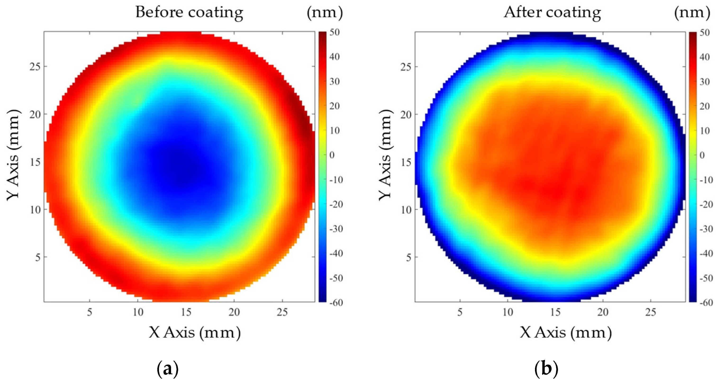
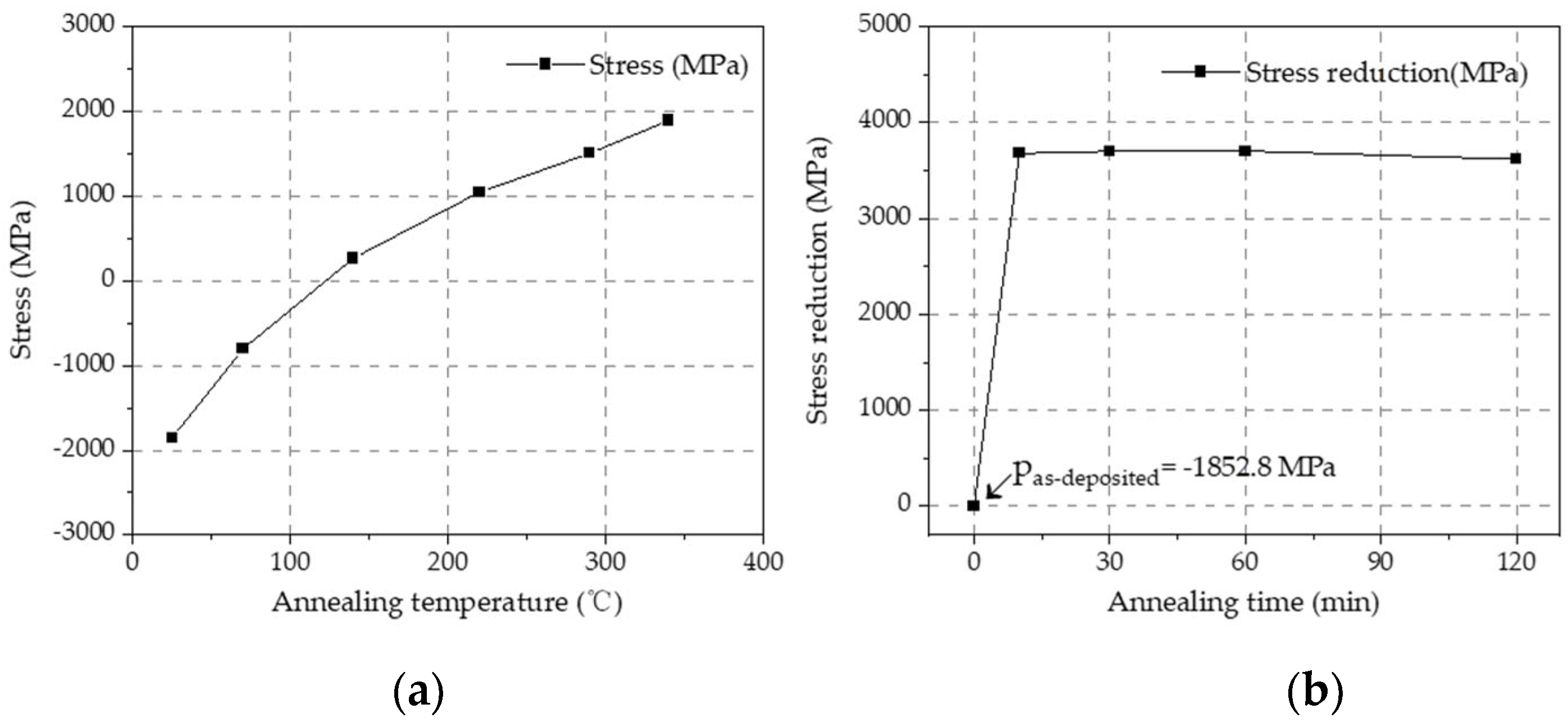
3.1. Change in Stress under Different Annealing Conditions

The intrinsic stress of the multilayer structures was determined through sample curvature measurements using a Fizeau interferometer to measure the surface contours and radii of curvature of the substrates before and after deposition, as illustrated in Figure 4. Subsequently, stress was calculated using the Stoney equation, and the stress measurement results are depicted in Figure 5. The as-deposited samples exhibited a compressive stress of approximately −1852.8 MPa. As observed in Figure 5a, the stress changes with the annealing temperature between 70 °C and 340 °C. The stress reached zero within the range of 70–140 °C, which corresponded to the transition from compressive to tensile stress. The change behavior of stress with temperature aligns with findings reported in numerous other multilayer systems [18,26]. Additionally, Figure 5b illustrates the changes in stress (p) with the annealing duration. Notably, before annealing at 340 °C for 10 min, the stress shifted from compressive to tensile. It is evident that stress changes occurred rapidly within the initial 10 min of annealing and likely during the heating process as well. Furthermore, compared to the temperature-dependent stress reduction, prolonged annealing did not result in significant changes in stress, a trend similarly observed in the Mo/B4C, Mo/Si, and W/Si multilayer systems [18,20,32].
The results of all the annealing experiments indicate that the annealing temperature between 70 °C and 140 °C resulted in a zero-stress state. Before annealing at 340 °C for 10 min, the stress changed significantly. However, extending the annealing duration to 120 min did not result in a significant change in the stress levels. It is evident that stress undergoes rapid changes 10 min before annealing and may also fluctuate during heating.

3.2. Post-Deposition Annealing with Different Temperature (First Group)

The GIXR curves of five samples before and after annealing at 70, 140, 220, 290, and 340 °C are shown in Figure 6. With the annealing temperature rising from 70 to 340 °C, the grazing angles of the Bragg peaks progressively decreased, indicating an increase in the thickness of the multilayer d-spacing. Additionally, the displacement of the diffraction peak location increased as the annealing temperature rose.
Based on the GIXR measurements, the change in the layered structure of the NiV/B4C multilayers was assumed to have occurred with the increase in the annealing temperature since all the parameters for the GIXR measurements and deposition remained constant, except for the annealing temperature. Therefore, the change in the higher-order Bragg peak may be caused by variations in the periodic thickness of the multilayer film and alterations in the interface roughness. For confirmation, the relevant parameters of the multilayer films were quantitatively fitted. Figure 6 shows the fitted result of the NiV/B4C multilayer annealed at 70 °C, and the fitted curve closely matched the GIXR measurement results, implying agreement between the fitting model and the deposited layer structure. The bandwidth of the measured Bragg peaks was similar to that of the fitted curve, indicating the good uniformity of the 100 bilayers. The changes in the interfacial roughness and diffusion resulted in a change in the interfacial width, as depicted in Figure 7a,b for the relative changes in the period and interface width, respectively. The GIXR and fitting curves were generated using IMD [33] software, and the results are shown in Table 1. The period expansion of the NiV/B4C multilayers is observed during the temperature annealing process. This increase in the multilayer thickness may be attributed to the expansion of boron carbide. Similar findings have been reported in previous studies [34,35].

3.3. Post-Deposition Annealing for Different Durations (Second Group)

The GIXR measurements and fitted results of the NiV/B4C multilayers before and after annealing for 10, 30, 60, and 120 min at 340 °C are depicted in Figure 8. The fitted curves closely matched the GIXR measurement results, implying agreement between the fitted model and the deposited layer structure. The relative changes in the period and interface width are illustrated in Figure 9a and 9b, respectively. According to the measurements, the Bragg peak shifted to a smaller angle, indicating an increase in the periodic thickness. Notably, the grazing angles of the Bragg peaks for all the annealed samples (in the first and second groups) showed a slight decrease compared to those of the as-deposited sample, suggesting alterations in the multilayer film structure. The detailed fitting results are presented in Table 2.

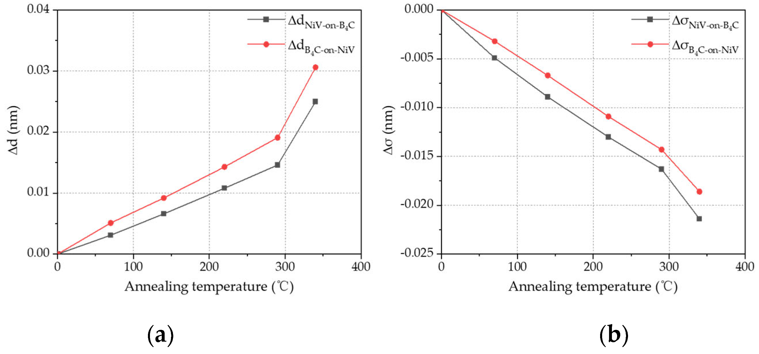
3.4. Microstructure Analysis before and after Annealing

To better understand the physics behind the changes in the reflectance, period, and stress during annealing, the X-ray rocking curves of the multilayers were tested before and after annealing. Two factors could have contributed to the changes in the X-ray reflectivity: different interface roughness and interdiffusion within the multilayers. Typically, the rocking curve measurements are utilized to analyze the scattering signals arising from the interface roughness. The scattering curves of the as-deposited multilayers and multilayers obtained under different annealing conditions are shown in Figure 10. The peak height corresponded to the interface roughness level. After annealing at 70, 140, 220, and 290 °C for 60 min, the intensity of both the conformal and non-conformal scattering remained relatively constant (within the detection limit). No obvious changes in roughness were observed. However, when the annealing temperature reached 340 °C, the scattering peak was notably enhanced, indicating an increase in the surface roughness of the multilayer films and structural changes at 340 °C. To further investigate the effect of annealing on the structure of the multilayer films at 340 °C, a constant-temperature annealing experiment was conducted. Following annealing at 340 °C, the scattering intensity continued to increase, while the roughness gradually increased over time, as depicted in Figure 10d.

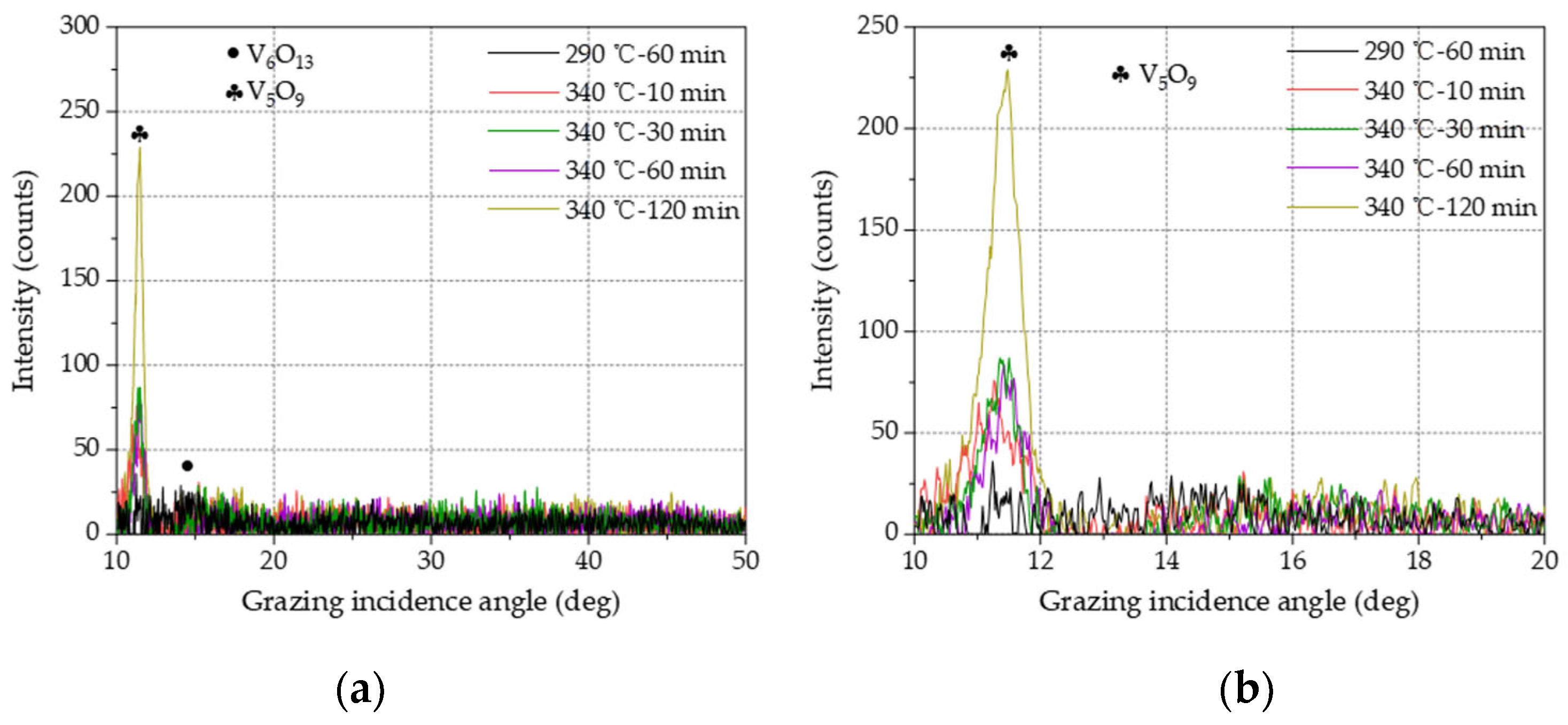
3.5. Grazing-Incidence X-ray Diffraction (GIXRD)

Based on the GIXR and X-ray diffuse scattering measurements, it was observed that the corresponding interface width decreased when the multilayer films were annealed at different temperatures. Annealing induces changes in the crystal structure, enhances interface clarity, releases stress, and leads to increased reflectivity and interface roughness. The physical model is shown in Figure 11.
GIXRD analyses were conducted to confirm crystallization, as illustrated in Figure 12a along with a magnified view (Figure 12b) of the (0 0 1) reflection of V5O9 (PDF#18–1450). Sharp peaks were absent when the annealing temperature was below 340 °C, as depicted in Figure 12a. At 340 °C, a noticeable (0 0 1) crystal-plane diffraction peak of V5O9 appeared at 2θ = 11.453°, consistent with its appearance in a prior study [36]. However, the crystal-plane diffraction peaks of V6O13 (2 0 0) (PDF#27-1318) were not clearly visible at other positions. Hence, V was well dispersed with Ni over the Si surfaces. Additionally, a noticeable shift in the (0 0 1) peak position towards a lower 2θ with increasing annealing temperature was observed, as depicted in Figure 12b, indicating the improved crystallinity of V5O9. These observations were consistent with the stress test results mentioned earlier. To understand the crystallization clearly, the Scherrer formula D = Kλ/(βcosθ) was utilized for calculating the grain size, with the results listed in Table 3 and depicted in Figure 13. The grain size gradually increased with the extension of the annealing duration, consistent with the earlier discussion.

3.6. GISAXS Analysis

Figure 14 displays the GISAXS measurements for the various annealing conditions of the NiV/B4C multilayers on a logarithmic scale. It highlights the prominent feature in GISAXS scattering, known as resonant diffuse scattering sheets or Bragg sheets [37], arising from the correlated interface roughness [38]. The spacing between the Bragg-like sheets in the qz space is inversely proportional to the multilayer period thickness (d) according to Δqz = 2π/d. As the annealing temperature increases, the scattering curve’s peak shape for the NiV/B4C multilayers slightly broadens, and the number of Bragg-like peaks remains mostly unchanged. This suggests changes in the interface roughness and lateral correlation length of the multilayer films, leading to the broadening of the Bragg sheets in the qx direction.
The lengths of the detected Bragg-like sheets in the qx space represent the distribution of the scattering intensity across spatial frequencies. The first and second sheets were utilized for calculating the average PSD function. Figure 15 illustrates the PSD functions of the NiV/B4C multilayers, demonstrating distinct characteristics with increasing temperature or annealing duration. The NiV/B4C multilayers maintained a relatively stable interface before the high-temperature (340 °C) heating treatment, but the interfaces changed progressively with increasing annealing duration. To understand the interface evolution process during the temperature treatments, all the PSD functions were quantitatively fitted to obtain different interface parameters, such as the roughness and lateral correlation length. Figure 15 illustrates the PSD functions and their corresponding fitting curves for the NiV/B4C multilayers under various annealing conditions. Figure 15a,b show that the PSD of the multilayer film remains relatively stable when the annealing temperature is below 340 °C, with an inflection point observed at 340 °C. However, the PSD curve consistently increases with prolonged annealing duration at 340 °C, indicating an increase in interface roughness, consistent with previous rocking curve results (as shown in Figure 15c,d).
Table 4 compares the lateral correlation length results obtained from the X-ray rocking curve scans and GISAXS measurements. The results obtained from the two test methods are generally consistent, as shown in Figure 16. The transverse correlation length curve showed a decreasing trend with increasing annealing duration, attributed to inter-film diffusion and recrystallization. Concurrently, the results from the swing curve in Section 3.4 indicate an increasing trend in the interface roughness of the NiV/B4C multilayers, consistent with the observed monotonic inverse relationship between roughness and lateral correlation length reported by R. V. Medvedev [39], R. E. Geer [40], and P. Siffalovic [37].

4. Conclusions

This study systematically investigates the microstructural changes and stress variations in periodic NiV/B4C multilayers under various annealing conditions. The stress changed with increasing annealing temperature from 70 to 340 °C. Specifically, the stress transitioned from compressive to tensile within the temperature range of 70–140 °C, reaching zero. The constant-temperature annealing experiments indicated that the stress changes primarily occurred within the initial 10 min of annealing, rendering prolonged annealing unnecessary. The results from the grazing-incidence X-ray reflectometry (GIXR), grazing-incidence X-ray diffraction (GIXRD), X-ray diffuse scattering, and grazing-incidence small-angle X-ray scattering (GISAXS) indicated that the thickness of the multilayers expanded after annealing. As the temperature and duration increased, the multilayer film underwent crystallization, leading to a gradual increase in the grain size and subsequently, a larger interface roughness. This phenomenon is the primary cause of changes in microstructure and stress. This study focused on periodic layers with a d-spacing of approximately 3 nm, providing insights into the effects of annealing on stable NiV/B4C multilayer structures. Additionally, the performance of the thicker NiV/B4C multilayer film was also studied, and the difference between its annealed condition and that of the 3 nm NiV/B4C was found to be worth further investigation.

Author Contributions

Conceptualization, C.C., H.J., Z.W. (Zhanshan Wang), Z.Z. (Zhe Zhang) and Z.Z. (Zhong Zhang); methodology, C.C., H.J., Z.W. (Zhanshan Wang), Z.Z. (Zhe Zhang) and Z.Z. (Zhong Zhang); software, C.C. and H.N.; validation, C.C., Z.Z. (Zhe Zhang). and Z.Z. (Zhong Zhang); formal analysis, C.C., J.H., S.X. and W.S.; investigation, C.C.; resources, Z.Z. (Zhong Zhang); data curation, C.C. and Z.W. (Zhenbo Wei); writing—original draft preparation, C.C.; writing—review and editing, C.C. and Z.W. (Zhenbo Wei); visualization, C.C.; supervision, Z.Z. (Zhong Zhang); project administration, Z.Z. (Zhong Zhang); funding acquisition, Z.Z. (Zhong Zhang). All authors have read and agreed to the published version of the manuscript.

Funding

This work was supported by the National Key Research and Development Program of China (2022YFF0709100) and the National Natural Science Foundation of China (NSFC) (12204353).

Institutional Review Board Statement

Not applicable.

Informed Consent Statement

Not applicable.

Data Availability Statement

The data will be made available on request.

Acknowledgments

The authors would like to thank the BL16B1 and BL10U1 beam line stations of the Shanghai Synchrotron Radiation Facility’s (SSRF) experimental sites and facilities that were provided.

Conflicts of Interest

The authors declare that they have no known competing financial interests or personal relationships that could have appeared to influence the work reported in this paper.

References

  1. Huang, Q.; Medvedev, V.; van de Kruijs, R.; Yakshin, A.; Louis, E.; Bijkerk, F. Spectral tailoring of nanoscale EUV and soft X-ray multilayer optics. Appl. Phys. Rev. 2017, 4, 14. [Google Scholar] [CrossRef]
  2. Barrett, R.; Baker, R.; Cloetens, P.; Morawe, C.; Tucoulou, R.; Vivo, A. Reflective Optics for Hard X-ray Nanofocusing Applications at the ESRF. Synchrotron Radiat. News 2016, 29, 10–15. [Google Scholar] [CrossRef]
  3. Windt, D.L. Advancements in Hard X-ray Multilayers for X-ray Astronomy. In Proceedings of the Conference on Optics for EUV, San Diego, CA, USA, 10–13 August 2015. [Google Scholar] [CrossRef]
  4. Feng, Y.F.; Qi, R.Z.; Jiang, L.; Huang, Q.S.; Li, T.Z.; Liu, G.C.; Li, W.B.; Yan, W.S.; Zhang, Z.; Wang, Z.S. Chemical Modification of B4C Films and B4C/Pd Layers Stored in Different Environments. Materials 2021, 14, 1319. [Google Scholar] [CrossRef] [PubMed]
  5. Shaposhnikov, R.; Polkovnikov, V.; Garakhin, S.; Vainer, Y.; Chkhalo, N.; Smertin, R.; Durov, K.; Glushkov, E.; Yakunin, S.; Borisov, M. Investigation of structural and reflective characteristics of short-period Mo/B4C multilayer X-ray mirrors. J. Synchrotron Radiat. 2024, 31, 268–275. [Google Scholar] [CrossRef] [PubMed]
  6. Yumoto, H.; Koyama, T.; Suzuki, A.; Joti, Y.; Niida, Y.; Tono, K.; Bessho, Y.; Yabashi, M.; Nishino, Y.; Ohashi, H. High-fluence and high-gain multilayer focusing optics to enhance spatial resolution in femtosecond X-ray laser imaging. Nat. Commun. 2022, 13, 8. [Google Scholar] [CrossRef] [PubMed]
  7. Jensen, C.P.; Madsen, K.K.; Christensen, F.E. Investigation of new material combinations for hard x-ray telescope designs. In Proceedings of the Conference on Space Telescopes and Instrumentation II—Ultraviolet to Gamma Ray, Orlando, FL, USA, 24–31 May 2006. [Google Scholar] [CrossRef]
  8. Carau, D.; Peffen, J.C.; Morawe, C. Thickness uniformity study on the ESRF multilayer deposition system. In Proceedings of the Conference on Advances in X-ray/EUV Optics and Components XII held as part of the SPIE Optics + Photonics Symposium, San Diego, CA, USA, 8–9 August 2017. [Google Scholar] [CrossRef]
  9. Leake, S.J.; Chahine, G.A.; Djazouli, H.; Zhou, T.; Richter, C.; Hilhorst, J.; Petit, L.; Richard, M.I.; Morawe, C.; Barrett, R.; et al. The Nanodiffraction beamline ID01/ESRF: A microscope for imaging strain and structure. J. Synchrot. Radiat. 2019, 26, 571–584. [Google Scholar] [CrossRef] [PubMed]
  10. Vaughan, G.B.M.; Baker, R.; Barret, R.; Bonnefoy, J.; Buslaps, T.; Checchia, S.; Duran, D.; Fihman, F.; Got, P.; Kieffer, J.; et al. ID15A at the ESRF—A beamline for high speed operando X-ray diffraction, diffraction tomography and total scattering. J. Synchrot. Radiat. 2020, 27, 515–528. [Google Scholar] [CrossRef]
  11. Wu, B.H.; Chung, C.K.; Shih, T.R.; Peng, C.C.; Mohanty, U.S. Effect of residual stress on nanoindented property of Si/C/Si multilayers. J. Micro-Nanolithogr. Mems. Moems. 2009, 8, 5. [Google Scholar] [CrossRef]
  12. Meyer, D.C.; Klingner, A.; Leisegang, T.; Holz, T.; Dietsch, R.; Paufler, P. Stressed states and self-organized structuring of W/C multilayers. MRS Online Proc. Libr. 2001, 695, 459–464. [Google Scholar] [CrossRef]
  13. Asadipour, H.; Ashrafizadeh, F.; Alizadeh, M. Graphene Layer Morphology and Oxidation Behavior Induced by Step Bunches Created on Copper Substrate. J. Mater. Eng. Perform. 2023, 32, 9735–9744. [Google Scholar] [CrossRef]
  14. Turjeman, I.; Dotan, T.; Berg, Y.; Kotler, Z.; Sherman, D.; Shacham-Diamand, Y. Mechanical modeling of metal thin films on elastomers for femtosecond laser patterned interconnects. Microelectron. Eng. 2021, 241, 7. [Google Scholar] [CrossRef]
  15. Nguyen, T.D.; Gronsky, R.; Kortright, J.B. Microstructure and Stability Comparison of Nanometer Period W/C, WC/C, and Ru/C Multilayer Structures. Mat. Res. Soc. Symp. Proc. 1990, 187, 95–100. [Google Scholar] [CrossRef]
  16. Nguyen, T.D.; Gronsky, R.; Kortright, J.B. Microstructure roughness interrelation in Ru/C and Ru/B4C X-ray multilayers. Mater. Res. Soc. Symp. Proc. 1992, 280, 161–166. [Google Scholar] [CrossRef]
  17. Geisz, J.F.; Kuech, T.F.; Lagally, M.G.; Cardone, F.; Potemski, R.M. Film stress of sputtered W/C multilayers and strain relaxation upon annealing. J. Appl. Phys. 1994, 75, 1530–1533. [Google Scholar] [CrossRef]
  18. Barthelmess, M.; Bajt, S. Thermal and stress studies of normal incidence Mo/B4C multilayers for a 6.7 nm wavelength. Appl. Optics 2011, 50, 1610–1619. [Google Scholar] [CrossRef] [PubMed]
  19. Huang, Q.; Zhang, J.; Qi, R.; Yang, Y.; Wang, F.; Zhu, J.; Zhang, Z.; Wang, Z. Structure and stress studies of low temperature annealed W/Si multilayers for the X-ray telescope. Opt. Express 2016, 24, 15620–15630. [Google Scholar] [CrossRef] [PubMed]
  20. Platonov, Y.; Broadway, D.; DeGroot, B.; Mao, P.; Harrison, F.; Gutman, G.; Rodriguez, J. X-ray reflectivity and mechanical stress in W/Si multilayers deposited on thin substrates of glass, epoxy-replicated aluminum foil, and Si wafer. In Proceedings of the Optical Science, Engineering and Instrumentation ’97, San Diego, CA, USA, 11 July 1997. [Google Scholar] [CrossRef]
  21. Salditt, T.; Metzger, T.H.; Peisl, J. Kinetic roughness of amorphous multilayers studied by diffuse X-ray scattering. Phys. Rev. Lett. 1995, 74, 1890. [Google Scholar] [CrossRef]
  22. Sinha, S.K.; Sirota, E.B.; Garoff, S.; Stanley, H.B. X-ray and neutron scattering from rough surface. Phys. Rev. B 1988, 38, 2297–2311. [Google Scholar] [CrossRef] [PubMed]
  23. Deboer, D.K.G. X-ray reflection and transmission by rough surfaces. Phys. Rev. B 1995, 51, 5297–5305. [Google Scholar] [CrossRef]
  24. Pape, I.; Hase, T.P.A.; Tanner, B.K.; Wormington, M. Analysis of grazing incidence X-ray diffuse scatter from Co-Cu multilayers. Physica B 1998, 253, 278–289. [Google Scholar] [CrossRef]
  25. Holy, V.; Baumbach, T. Nonspecular X-ray reflection from rough multilayers. Phys. Rev. B 1994, 49, 10668–10676. [Google Scholar] [CrossRef]
  26. Asadchikov, V.E.; Kozhevnikov, I.V.; Krivonosov, Y.S.; Mercier, R.; Metzger, T.H.; Morawe, C.; Ziegler, E. Application of X-ray scattering technique to the study of supersmooth surfaces. Nucl. Instrum. Methods Phys. Res. Sect. A-Accel. Spectrom. Dect. Assoc. Equip. 2004, 530, 575–595. [Google Scholar] [CrossRef]
  27. Li, H.C.; Zhu, J.T.; Wang, Z.S.; Chen, H.; Wang, Y.Z.; Wang, J. Integration method for directly analyzing interface statistics of periodic multilayers from X-ray scattering. J. Synchrot. Radiat. 2014, 21, 97–103. [Google Scholar] [CrossRef]
  28. Jiang, H.; Hua, W.Q.; Tian, N.X.; Li, A.G.; Li, X.H.; He, Y.M.; Zhang, Z.Y. In situ GISAXS study on the temperature-dependent performance of multilayer monochromators from the liquid nitrogen cooling temperature to 600 °C. Appl. Surf. Sci. 2020, 508, 8. [Google Scholar] [CrossRef]
  29. Payne, A.P.; Clemens, B.M. Influence of roughness distributions and correlations on X-ray diffraction from superlattices. Phys. Rev. B 1993, 47, 2289–2300. [Google Scholar] [CrossRef] [PubMed]
  30. Wang, X.; Zheng, W.T.; Gao, L.J.; Wei, L.; Guo, W.; Bai, Y.B.; Fei, W.D.; Meng, S.H.; He, X.D.; Han, J.C. Surface morphology and dynamic scaling in growth of iron nitride thin films deposited by dc magnetron sputtering. J. Vac. Sci. Technol. A 2003, 21, 983–987. [Google Scholar] [CrossRef]
  31. Kardar, M.; Parisi, G.; Zhang, Y. Dynamic Scaling of Growing Interfaces. Phys. Rev. Lett. 1986, 56, 889–892. [Google Scholar] [CrossRef]
  32. Montcalm, C. Reduction of residual stress in extreme ultraviolet Mo/Si multilayer mirrors with postdeposition thermal treatments. Opt. Eng. 2001, 40, 469–477. [Google Scholar] [CrossRef]
  33. Windt, D.L. IMD—Software for modeling the optical properties of multilayer films. Comput. Phys. 1998, 12, 360–370. [Google Scholar] [CrossRef]
  34. Rao, P.N.; Rai, S.K.; Sinha, A.K.; Singh, M.N.; Lodha, G.S. Thermally induced interface changes in W/B4C multilayers. Thin Solid Films 2015, 589, 268–271. [Google Scholar] [CrossRef]
  35. Naujok, P.; Murray, K.; Yulin, S.; Patzig, C.; Kaiser, N.; Tünnermann, A. Thermal stability of B-based multilayer mirrors for next generation lithography. Thin Solid Films 2017, 642, 252–257. [Google Scholar] [CrossRef]
  36. Caravaggio, G.A.; Detellier, C.; Wronski, Z. Synthesis, stability and electrochemical properties of NiAl and NiV layered double hydroxides. J. Mater. Chem. 2001, 11, 912–921. [Google Scholar] [CrossRef]
  37. Siffalovic, P.; Majkova, E.; Chitu, L.; Jergel, M.; Luby, S.; Keckes, J.; Maier, G.; Timmann, A.; Roth, S.V.; Tsuru, T.; et al. Characterization of Mo/Si soft X-ray multilayer mirrors by grazing-incidence small-angle X-ray scattering. Vacuum 2009, 84, 19–25. [Google Scholar] [CrossRef]
  38. Kaganer, V.M.; Stepanov, S.A.; Kohler, R. Effect of roughness correlations in multilayers on Bragg peaks in X-ray diffuse scattering. Physica B 1996, 221, 34–43. [Google Scholar] [CrossRef]
  39. Medvedev, R.V.; Nikolaev, K.V.; Zameshin, A.A.; Ijpes, D.; Makhotkin, I.A.; Yakunin, S.N.; Yakshin, A.E.; Bijkerk, F. Low-energy ion polishing of Si in W/Si soft X-ray multilayer structures. J. Appl. Phys. 2019, 126, 10. [Google Scholar] [CrossRef]
  40. Geer, R.E.; Qadri, S.B.; Shashidhar, R.; Thibodeaux, A.F.; Duran, R.S. Off-specular x-ray scattering in Langmuir-Blodgett multilayers of a liquid-crystalline polymer. Phys. Rev. E 1995, 52, 671–680. [Google Scholar] [CrossRef]
Figure 1. Annealing temperature control curve of NiV/B4C multilayer film for (a) temperature dependence and (b) time dependence analyses.
Coatings 14 00513 g001
Figure 2. Macro view of the NiV/B4C multilayer and sample stage.
Coatings 14 00513 g002
Figure 3. Geometry of the GISAXS technique.
Coatings 14 00513 g003
Figure 4. (a) Surface profile of NiV/B4C multilayer film before coating; (b) surface profile of NiV/B4C multilayer film after coating.
Coatings 14 00513 g004
Figure 5. (a) Temperature-dependent stress curve of NiV/B4C multilayers; (b) stress reduction in the multilayers after annealing at 340 °C for different annealing durations.
Coatings 14 00513 g005
Figure 6. GIXR measurement and fitted result of NiV/B4C multilayers under different annealing temperatures.
Coatings 14 00513 g006
Figure 7. Relative changes in the (a) period and (b) interface width of the multilayer after annealing at different temperatures for 60 min.
Coatings 14 00513 g007
Figure 8. GIXR measurement and fitted result of NiV/B4C multilayers under different annealing time.
Coatings 14 00513 g008
Figure 9. Relative changes in the (a) period and (b) interface width of the multilayers after annealing at 340 °C for different durations.
Coatings 14 00513 g009
Figure 10. Rocking curves around the 1st Bragg peak of the (a) multilayers annealed at 70, 140, 220, 290, and 340 °C for 60 min; (b) comparison of curves before and after annealing; (c) multilayers annealed at 340 °C for 10, 30, 60, and 120 min; (d) comparison of curves before and after annealing (the curves of different color are measurements, black curve is a fitting result).
Coatings 14 00513 g010
Figure 11. Process of interface changes during annealing of the as-deposited multilayer NiV/B4C coatings.
Coatings 14 00513 g011
Figure 12. (a) GIXRD patterns of the film annealed at different conditions. (b) Magnified view of the (0 0 1) reflection of V5O9.
Coatings 14 00513 g012
Figure 13. Grain size of V5O9(0.01) crystal phase at 2θ = 11.453° after annealing NV/B4C multilayers.
Coatings 14 00513 g013
Figure 14. GISAXS maps of NiV/B4C multilayers measured at different annealing conditions.
Coatings 14 00513 g014
Figure 15. PSD functions of (a) different annealing temperatures; (b) fitting curves; (c) different annealing durations; and (d) fitting curves.
Coatings 14 00513 g015
Figure 16. The lateral correlation length for IMD and GISAXS at different annealing (a) temperatures; and (b) different annealing durations.
Coatings 14 00513 g016
Table 1. IMD fitting data of the multilayer film after annealing at different temperatures for 60 min.
Temperature (°C)Period Thickness d (nm)ΔdNiV(nm)ΔdB4C (nm)ΔσNiV-on-B4C (nm)ΔσB4C-on-NiV (nm)
As-DepositedAnnealed
703.04833.05650.00310.0051−0.0049−0.0032
1403.07963.09540.00660.0092−0.0089−0.0067
2203.08163.10680.01080.0143−0.0130−0.0109
2903.05933.09300.01460.0191−0.0163−0.0143
3403.06643.12190.02500.0306−0.0214−0.0186
Table 2. IMD fitting data of the multilayer film with extended annealing duration.
Time (min)Period Thickness d (nm)ΔdNiV (nm)ΔdB4C (nm)ΔσNiV-on-B4C (nm)ΔσB4C-on-NiV (nm)
As-DepositedAnnealed
103.06133.11250.02280.0284−0.0045−0.0033
303.04483.09780.02370.0293−0.0113−0.0092
603.06643.12190.02500.0306−0.0214−0.0186
1203.08383.14450.02760.0331−0.0415−0.0381
Table 3. Grain size of V5O9(0.01) crystal phase at 2θ = 11.453° after annealing NV/B4C multilayers.
SampleGrain Size (nm)
340 °C for 10 min1.0834
340 °C for 30 min1.4159
340 °C for 60 min1.4961
340 °C for 120 min2.5909
Table 4. The lateral correlation length for IMD and GISAXS with different annealing conditions.
Annealing Conditionsξ//-IMD (nm)ξ//-GISAXS (nm)Δξ// (nm)
70 °C for 60 min 14.792414.7247−0.0677
140 °C for 60 min14.575614.5321−0.0435
220 °C for 60 min14.340514.2961−0.0444
290 °C for 60 min14.053614.0190−0.0346
340 °C for 60 min12.764112.3337−0.4304
340 °C for 10 min14.147714.0571−0.0906
340 °C for 30 min13.812713.6325−0.1802
340 °C for 60 min12.764112.3337−0.4304
340 °C for 120 min10.665510.3728−0.2927
Disclaimer/Publisher’s Note: The statements, opinions and data contained in all publications are solely those of the individual author(s) and contributor(s) and not of MDPI and/or the editor(s). MDPI and/or the editor(s) disclaim responsibility for any injury to people or property resulting from any ideas, methods, instructions or products referred to in the content.

