

Utilizing Metal Oxide Thin Films for Device Engineering of Solution-Processed Organic Multi-Junction Solar Cells
Condensed Matter Physics Group, Department of Physics, Kuwait University, P.O. Box 5969, Safat 13060, Kuwait
Coatings 2024, 14(5), 525; https://doi.org/10.3390/coatings14050525
Submission received: 14 March 2024
/
Revised: 18 April 2024
/
Accepted: 23 April 2024
/
Published: 24 April 2024
(This article belongs to the Special Issue Advanced Metal Oxide Films: Materials and Applications)
Abstract
:Electron and hole transporting layers play a major role in high-performance and stable organic-based optoelectronic devices. This paper demonstrates detailed device engineering of multi-junction organic photovoltaics built on two different metal oxide-based electron and hole transport (buffer) layers prepared by thermal or solution-processed methods. The main focus is on the device processing parameters as well as practical details of preparation of buffer layers to give the research community a clear, step-by-step recipe to successfully replicate and build series and parallel connected multi-junction solution-based organic solar cells for their needs. Here, the recipes and deposition conditions of two metal oxide buffer layers are presented in detail, based on basic commercially available materials and tools, to achieve well-engineered tandem (multi-junction) solution-processed organic solar cells. The buffer layers have appropriate energy levels for electrical selectivity of anode and cathode electrodes, and they are highly stable and chemically compatible with processing of solution-based polymer solar cells. To demonstrate the engineering steps of multi-junction devices, the PCE10:PC70BM blend is used as the active layer for all subcells. Then, to improve the power conversion efficiency of the single-junction photovoltaic device, PCE10:PC70BM blend is used in combination with DPPx:PC70BM with different absorption spectra for bottom and top subcell active layers. An optimized series tandem device with 10.6% power conversion efficiency is demonstrated. Generally, the device structures reported here can also be used for other types of optoelectronic devices, such as light emitting diodes and photodetectors.
1. Introduction
Organic semiconductor films have recently demonstrated their potential for use in photovoltaic active layers. Efficiency and stability improvements in recent decades have opened up new possibilities for different applications and have brought the commercialization of such technologies for large-scale production of solar cells much closer [1,2,3,4]. Their mechanical flexibility, light weight, optical transparency, and color tunability make them suitable for window applications and flexible electronics [5]. Since they can be processed at low temperatures and via fast solution-processing methods (blade, roll-to-roll, and print coating) for coating of the precursor solutions, production costs can be lowered, leading to cheaper, large-scale installation of future solar cell power plants [6,7,8]. In addition to the power conversion efficiency, the stability of the organic solar cells must be improved before they can be commercialized. Their sensitivity to moisture and UV light are the two most important issues to address. Very good encapsulation in combination with a UV filter can improve their stability under working conditions. Another point to discuss is the choice of electrodes. Organic semiconductors are generally very soft and when metallic layers such as copper, silver, or aluminum are used as top electrode, under working conditions, they can produce small metallic particles penetrating into the organic active layer leading to recombination of generated electrons and holes. One of the ways to avoid this problem is to use conductive oxide-based electrodes such as ITO for the top electrode. Then, if an opaque device is desirable, the ITO top electrode can be covered with a metallic layer (Cu, Ag, Al) to act as a mirror. In this case, the ITO layer, which is mechanically harder and more compact, will protect the soft underlying organic layers against the penetration of metallic particles. Having a transparent organic solar cell also allows its use in window applications (built-in solar cell). Organic solar cells can be processed on plastic flexible substrates such as PET and can play an important role in flexible electronics generally. Imagine having a power supply on your clothing! Organic flexible solar cells can be used anywhere transparency, flexibility, and light weight are important to achieve [9,10,11,12]. An efficient and stable solar cell can only be achieved by a combination of optimized high-quality organic donor and acceptor materials, optimum processing conditions, and precise engineering of the whole device. Usually, indium tin oxide (ITO) covered glass for rigid cells, or ITO covered PET (or PEN) for flexible solar cells, is used with a transparent electrode in combination with a metallic top electrode (Al, Ag, Cu). The active layer of the device must be processed between two buffer layers, avoiding direct contact with electrodes, so that the combination of each electrode with a buffer layer can extract electrons and holes efficiently and selectively. Direct contact between the active layer and electrodes leads to electron-hole recombination at their interfaces, causing reduction of the photo-generated current and fill factor of the device, and considerably reducing the power conversion efficiency. In this context, electron and hole transport layers play a very important role [13,14,15]. The electronic energy levels of the buffer layer must be matched with the valence and conduction band energy levels of the semiconductor with sufficient electrical conductivity and high optical transparency [16,17]. In addition, buffer layer process compatibility, chemical stability, and cost must be considered. All these issues require very precise recipes and processing methods for an optimum device, even more so when multi-junction devices, as opposed to single-junction types, are being considered [18,19,20]. For solution-processed devices, organic materials (polymers, fullerenes) must be dissolved into non-polar chlorinated solvents such as Chlorobenzene (CB), Dichloro-benzene (ODCB), or Chloroform. The buffer layer processed under the active layer must be chemically stable (compatible) with such a solvent. Generally, organic thin films have thicknesses of 80 to 120 nm and are very smooth with roughness between 1 to 3 nm. This means that, in addition to choose suitable materials and proper processing steps, a buffer layer deposited onto an organic active layer can be very thin as well (from 1 up to 10 nm as we will discuss later). The hole and electron transport layers of a tandem (multi-junction) solution-processed organic solar cell provide electrical selectivity of the electrodes to extract charge carriers efficiently, and also protect the underlying subcells against solvents. Therefore, it is always a challenge to address those two requirements at once. Here, the recipes of two metal oxide buffer layers are presented, composed of very basic and unexpensive commercially available materials (from Sigma Aldrich, St. Louis, MO, USA). In addition, their deposition conditions are fully explained. By following the steps reported in the manuscript and by using basic tools available in any research laboratory, such as spin coater and thermal evaporation systems, one can repeat and reproduce a very well-engineered tandem (multi-junction) device with series and parallel configurations. Therefore, this report can act as a very useful starting point for exploring organic single- and multi-junction devices. The main purpose of this article is to provide the research community with very clear and detailed device engineering of multi-junction polymer-based organic photovoltaics which are made with metal oxide buffer layers, and which have been used by the author for many years in his research on opto-electronic devices. The reader will be able to generate these structures quite easily and use them for their own purposes. Note that the objective here is only to explain the device engineering steps, not the efficiency of the solar cell devices, since the light to power conversion is strongly related to the choice and quality of the organic donor and acceptor materials used, which is not within the scope of this report. It must be noted that recent improvements and increased performance of organic solar cells are fully due to optimized state-of-the-art organic materials [21,22]. Here, the performance of optimized devices is limited by the materials which were available and, therefore, if the same device structures in this work can be combined with recent newly developed high-performance organic donor and acceptor materials, much higher performance will be generated relatively easily. Usually, to demonstrate the electronic abilities of multi-junction structures, the open-circuit voltage (Voc) and fill factor (FF) are the most important parameters to consider. Both open-circuit voltage (Voc) and fill factor (FF) are strongly related to the interfaces of active layers with buffer layers and electrodes, and to the whole device structure in general. In contrast, the photogenerated current and, therefore, the power conversion efficiency is more directly related to the polymer or fullerene’s chemical and optical properties as the active layer of the device, and also the illumination conditions [23,24]. In this article, engineering of four different device structures will be demonstrated. Two single-junction devices with so-called conventional and inverted [25,26,27] structures will be reported. Then, two types of multi-junction device are presented in which the subcells are electrically connected in series or parallel configurations. An organic solar cell with conventional structure is made as Glass/ITO electrode (transparent)/HTL/Organic Active Layer/ETL/Metallic electrode (opaque) while the inverted structure is built as Glass/ITO electrode (transparent)/ETL/Organic Active Layer/HTL/Metallic electrode (opaque). It must be noted that, instead of ITO, any type of optically transparent electrode (such as FTO or high conductive PEDOT:PSS) can be used, and similarly for the metallic top electrode materials such as silver (Ag), aluminum (Al), gold (Au) and copper (Cu). Here, the single-junction device with conventional structure is made of 0.7 mm Glass/150 nm ITO/20 nm MoO3/Organic Active Layer/3 nm TiO2/150 nm Ag and the single-junction solar cell with inverted configuration is made of 0.7 mm glass/150 nm ITO/3 nm TiO2/Organic Active Layer/20 nm MoO3/150 nm Ag. The thickness of the organic active layer is varied (by coating with different spin speeds) until optimum electrical performance is achieved. The single-junction device structures are demonstrated in Figure 1.
A multi-junction device [28,29,30,31,32] can then be created by stacking subcells with structures similar to the above-mentioned single junctions onto each other. However, great attention must be paid to optical transparency, electrical properties, and to the chemical and physical stability of the interlayers connecting the subcells, especially in our case when the organic active layer is solution-processed by using methods such as spin, blade, roll-to-roll, and print coating. The series tandem (multi-junction) devices are made by stacking two or more subcells with inverted configuration as 0.7 mm Glass/150 nm ITO/3 nm TiO2/Organic Active Layer/20 nm MoO3 + 1 nm Ag + 3 nm TiO2/Organic Active/20 nm MoO3/150 nm Ag. The parallel tandem (multi-junction) devices are built up based on two or more subcells with both inverted and conventional structures as 7 mm Glass/150 nm ITO/3 nm TiO2/Organic Active Layer/20 nm MoO3 + 15 nm Ag +20 nm MoO3/Organic Active Layer/3 nm TiO2/150 nm Ag. The thickness of the organic active layers is varied for subcells to maximize electrical performance. It must be noted here that, generally, to increase the power conversion efficiency of multi-junction structures compared to single junctions, active layers must have non-overlapped optical spectra with high electrical performances. Also, the middle electrode connecting subcells must be optically as transparent as possible. In a series tandem (multi-junction) solar cell, the middle electrode connecting two subcells must have perfect charge extraction selectivity to extract electrons and holes efficiently from subcells but does not have to be electrically conductive since the middle electrode does not transport any charges. This interlayer acts as a recombination site for electrons and holes arriving from the bottom and top subcells, respectively. Therefore 1 nm silver (Ag) is used between the MoO3 and TiO2 buffer layers to provide the necessary recombination sites, leading to optimum extracted photocurrent (Jsc), open-circuit voltage (Voc), fill factor (FF), and performance of the tandem (multi-junction) device. For parallel tandem devices, at least 20 nm Ag was needed here to create a conductive middle electrode since, in this configuration, the connecting electrode must be used to extract holes from both subcells and must have sufficient electrical sheet conductivity to do so. Generally, if a much more transparent conductive electrode, such as ITO, is used instead of a metallic-based electrode such as Ag, the performance of the parallel tandem device will be improved due to higher light intensity illumination of the top subcell. Due to the softness and heat sensitivity of organic materials, a very soft sputtering process must be used with low sputtering power; also, the substrate must be cooled down (with liquid nitrogen) in combination with a large distance (20 cm or more) between the sputtering head and the substrate, in order to limit mechanical and thermal damage to the soft organic active layer during the sputtering process. It must be noted here that due to lack of a suitable sputtering tool, a metallic layer (Ag) had to be utilized instead. We will show that the series-connected tandem devices will be a suitable choice when two different polymers (active layers) are used with non-overlapping absorption spectra. The bottom subcell, based on PCE10 polymer, absorbs mainly in the blue region while the top subcell, based on DPPx polymer, absorbs longer wavelengths so that the series tandem device covers a broader range of the sunlight spectrum, leading to higher performance. Here, the parallel tandem structure based on a middle electrode with high optical absorption mainly on a longer wavelength (Ag absorption), limits its efficiency due to a lower light intensity available to illuminate the top subcell. Since the optical transmission of the metallic layer, such as silver, is higher in the blue region of the spectrum, for both bottom and top subcells in this report PCE10 polymer is used, and the performance of the single-junction device is slightly improved. It will be demonstrated that an optimum thickness of the active layer based on PCE10 polymer is about 260 nm for a single-junction device; by using a parallel tandem structure having thicknesses of 190 nm and 90 nm for bottom and top subcells, respectively, leading to total active layer thickness of 280 nm, the total absorption intensity is improved and therefore also the performance of the whole device compared to the single-junction model. The thickness of the middle electrode in both series and parallel tandem (multi-junction) configurations must be defined due to its capability to protect the underlying subcell during solution processing of the following top subcell. If this connecting electrode is not closed and chemically stable against chlorinated solvents, the underlying subcell will be dissolved during the coating of the next subcell processed on top of it, and no tandem (or multi-junction) device can be made. The chemical stability and compactness of the interlayer is, therefore, the most important initial requirement to address. The thermal deposition method is used here for MoO3 layer to ensure the compactness (hole-free layer) of the middle electrode in this report for all tandem (multi-junction) devices. Then, based on optical and electrical simulations and experimental process parameters, the thickness of the organic active layers can be varied, and an optimum device configuration can be achieved. The series- and parallel-connected tandem device structures are demonstrated in Figure 2.
To build up multi-junction devices, we can just stack more (three, four, and so on) subcells similar to the tandem structures of Figure 2. The same single- and multi-junction device structures can also be used for light emitting diodes and photodetectors. The same single-junction device structures (conventional and inverted) presented here can be used as a photo-detector. Also, for single color light emitting diodes, we can use a similar single-junction device structure but of course with different organic active layers. If we want to create multi-color light emitting diodes, we have to create a multi-junction device in which all subcells can be electrically connected individually, and therefore the example of parallel tandem solar cell shown here can be utilized but of course with all electrodes based on transparent ITO. The sputtering of conductive and transparent electrodes onto soft organic layers is a challenging task.
2. Materials and Methods
ITO and Ag were used in all four device structures as transparent and opaque electrodes, respectively. For hole transport (HTL) and electron transport layers (ETL), thermally evaporated Molybdenum Oxide (MoO3) and titanium dioxide (TiO2) dispersion processed at room temperature were used, respectively. Different thicknesses of both buffer layers are needed for each type of device structure. The main goal is to use the minimum thicknesses possible for the metal oxide buffer layers since they are much less electrically conductive than electrodes, and thicker films will increase the series resistance of the whole device, thus lowering the fill factor (FF) and performance significantly. However, the buffer layers must also be thick enough to give the electrodes a perfect selectivity to avoid extraction of both electrons and holes at the same electrode leading to interface recombination processes and lowering the electrical performance of the device. For an optimum device structure, 20 nm MoO3 as hole transport layer (HTL) and 3 nm TiO2 as electron transport layer (ETL) are used in this report. Both buffer layers are highly transparent, and their conduction and valence band energy levels perfectly match the HOMO and LUMO levels of the organic active layers, so that an optimum open-circuit voltage (Voc) and fill factor (FF) can be achieved.
The electron transport layer made of Titanium Oxide dispersion TiO2 used here [33] is a patented recipe (USPTO patent application number: 20120207947A1 and European Patent EP 2490235B1) which is a very stable dispersion solution in alcohol and can be coated under or onto the organic active layer without need for any thermal post-treatment at room temperature. The solvent dispersion can be any type of alcohol and is used for different coating tools, such as blade and roll-to-roll coaters instead of spin coating since higher boiling points are more suitable for them. The TiO2 dispersion has a good wetting with ITO-covered substrates and also onto organic active layers, leading to the possibility of using it for both conventional, inverted, and multi-junction device structures. This recipe begins with a relatively concentrated but stable TiO2 dispersion which can be further diluted with any type of alcohol (Ethanol, Methanol, Isopropyl alcohol, Butanol) before use. Note that all materials used here were purchased from Sigma Aldrich and the preparation steps were done inside a nitrogen-filled glove box. At room temperature, add in a 24 mL bottle with open cap and stirring magnet, 3 mg Di-sorbitol and 1 mL IPA (or ethanol) and stir at 300 to 600 rpm until all D-Sorbitol is dissolved and a perfectly clear solution is made. Add 0.5 mL Ethanolamine to this mixture and keep stirring as before. In a separate small bottle, outside the glove box, mix a small amount of Acetic Acid with pure water (1:0.5 volume %) and bring this mixture, sealed, inside the glove box. It is important to make only a small amount of this mixture since we do not want to introduce an unnecessarily large amount of water into the glove box. Slowly add 0.2 mL of acid/water mixture to the 24 mL bottle containing alcohol/D-sorbitol/Ethanolamine mixture and keep the whole mixture at the stirring plate unsealed until the smoke and heat that is generated has gone. After waiting for about 10 min, carefully add, dropwise, 0.5 mL Isopropoxide IV Titanium into the mixture while stirring the solution as before. Some heat and smoke will again be generated but will disappear after a couple of minutes as the solution cools down to RT. The final step is to add 20 mL IPA, Ethanol, or any type of alcohol to the mixture. This gives the final product, the TiO2 dispersion gel, which is a very clear solution and remains stable for a very long time. Before use, 0.2 mL of dispersion gel must be diluted further with 3 mL IPA, Ethanol, or any type of alcohol. The diluted TiO2 dispersion is spin coated inside the nitrogen filled glove box at 1000 rpm, 5000 acceleration, 60 s for all devices leading to a thickness of about 3 nm. It is more practical to keep the dispersion in concentrated form since, to get optimum results, the dilution must be adjusted based on coating tools and the boiling point of the alcohol which has been used. Note that the coating of TiO2 solution can be done inside or outside the glove box and at room temperature without need for any post-annealing. The TiO2 electron transport layer is ready directly after coating.
The hole transport layer made of Molybdenum Oxide (MoO3) is processed by thermal evaporation deposition method by using MoO3 powder. A crucible/heater evaporation source is used under 10−6 mbar pressure for this deposition. It is important to heat up the MoO3 powder slowly to limit the loss of its oxygen during the thermal evaporation process. A heat source based on a crucible/heater is a better choice than thermal evaporation boats in order to control the heat and keep the evaporation rate at about 1 Angstrom/second during the whole process more efficiently. Different MoO3 thicknesses were used based on the device structure, as explained before. A thermal evaporation method [34,35] was used instead of solution processing because a stable and compact buffer layer was needed to protect the underlying organic layers against chlorinated solvents, and because thermally evaporated MoO3 is much more compact and protective compared to some solution-processed dispersions described in the literature. To achieve high-quality and reproducible results, after each evaporation the crucible must be dry-cleaned and new fresh MoO3 powder must be used. Fresh MoO3 powder has a light green color which changes color to gray after one evaporation, indicating that it has already lost some of its oxygen content which will result in higher resistivity of the buffer layer and will increase the series resistance of the solar cell. This will result in lowering of the fill factor (FF) of the device.
The organic active layers were made of different polymers as donor materials with different bandgaps mixed with fullerene molecules PC70BM or PC60BM as acceptor components. All preparations and processing were done in a nitrogen (N2)-filled glove box. The PCE10:PC70BM solution was made by dissolving 10 mg PCE10 polymer (from 1-Materials company, Dorval, QC, Canada) + 20 mg PC70BM (from Nano-C company, Westwood, MA, USA) in 1 mL ODCB (Sigma Aldrich) at room temperature and with a stirring time of 24 h. Before spin coating, the solution was warmed up to 60 °C and processed by keeping the temperature at 60 °C with spin speeds between 500 to 1000 rpm for 60 s to achieve films with different thicknesses. No post-annealing was needed for this organic film. The DPPx:PC70BM solution was made by dissolving 3.5 mg DPPx polymer (from BASF company, Waterloo, Belgium) + 7 mg PC70BM or 7 mg PC60BM (from Nano-C company) into 1 mL solvent mixture of CF:ODCB (4:1 volume %) at room temperature and with a stirring time of 24 h. A spin program of 1000 rpm for 60 s was used, while the solution was kept at room temperature leading to an optimum thickness of about 90 nm. No thermal post-annealing was done. The P3HT:PC60BM solution was made by dissolving 30 mg P3HT (Rieke materials company, Lincoln, NE, USA) + 30 mg PC60BM (Nano-C company) into 1 mL ODCB with stirring at room temperature for 24 h. The film was coated with spin speed of 1000 rpm for 60 s and the coated substrate was placed directly after spin coating under a cap to dry slowly at room temperature for 30 min. The thermal post-annealing was then done at 130 °C for 10 min. A film thickness of 300 nm was achieved.
In all cases, the substrates were cleaned by ultrasonication at room temperature in demi water + soap solution for 10 min followed by washing with demi water to completely remove the soap. Then, ultrasonication in acetone and IPA was performed, each for 10 min at room temperature, and the samples were dried with a nitrogen gun. UV-Ozone treatment was then performed for 20 min before inserting the substrates inside a nitrogen-filled glove box in which all processes and measurements were carried out. Here, as a starting point, single- and multi-junction devices are presented based on PCE10:PC70BM to demonstrate the device engineering processes. Then, a series tandem device is reported using a PCE10:PC70BM bottom cell + DPPx:PC70BM top cell which shows the capability of tandem structures with subcells with non-overlapping absorption spectra to improve on single-junction devices by harvesting the spectrum of sunlight more efficiently. The parallel tandem device is made of PCE10:PC70BM blend for both bottom and top subcells. The top cell in this case has much lower light intensity of longer wavelengths due to using silver for the middle electrode and therefore blue-absorbing PCE10:PC70BM polymer is more compatible. In this case, the total active layer thickness was improved from 260 for the single-junction device to 280 nm for the parallel tandem device, leading to a higher generated current. It must be noted here that by keeping all parameters the same but by using ITO instead of Ag, the parallel tandem configuration can be as efficient as the series configuration in which different polymers with no overlapped optical absorption spectra are utilized. The P3HT:PC60BM single-junction device is only used to demonstrate the variation of electrical parameters (Voc, Jsc, FF, and performance) under lower light intensities to explain the behavior of the multi-junction structures more clearly. In order to optimize the series tandem cell with two different polymers (with non-overlapping absorption spectra), optical and electrical simulations and many other experiments were performed to achieve the best results possible using the previously mentioned materials and device structures. For the parallel tandem device, experimental work was done to create different thicknesses for both bottom and top subcells to find an optimum output.
3. Results and Discussion
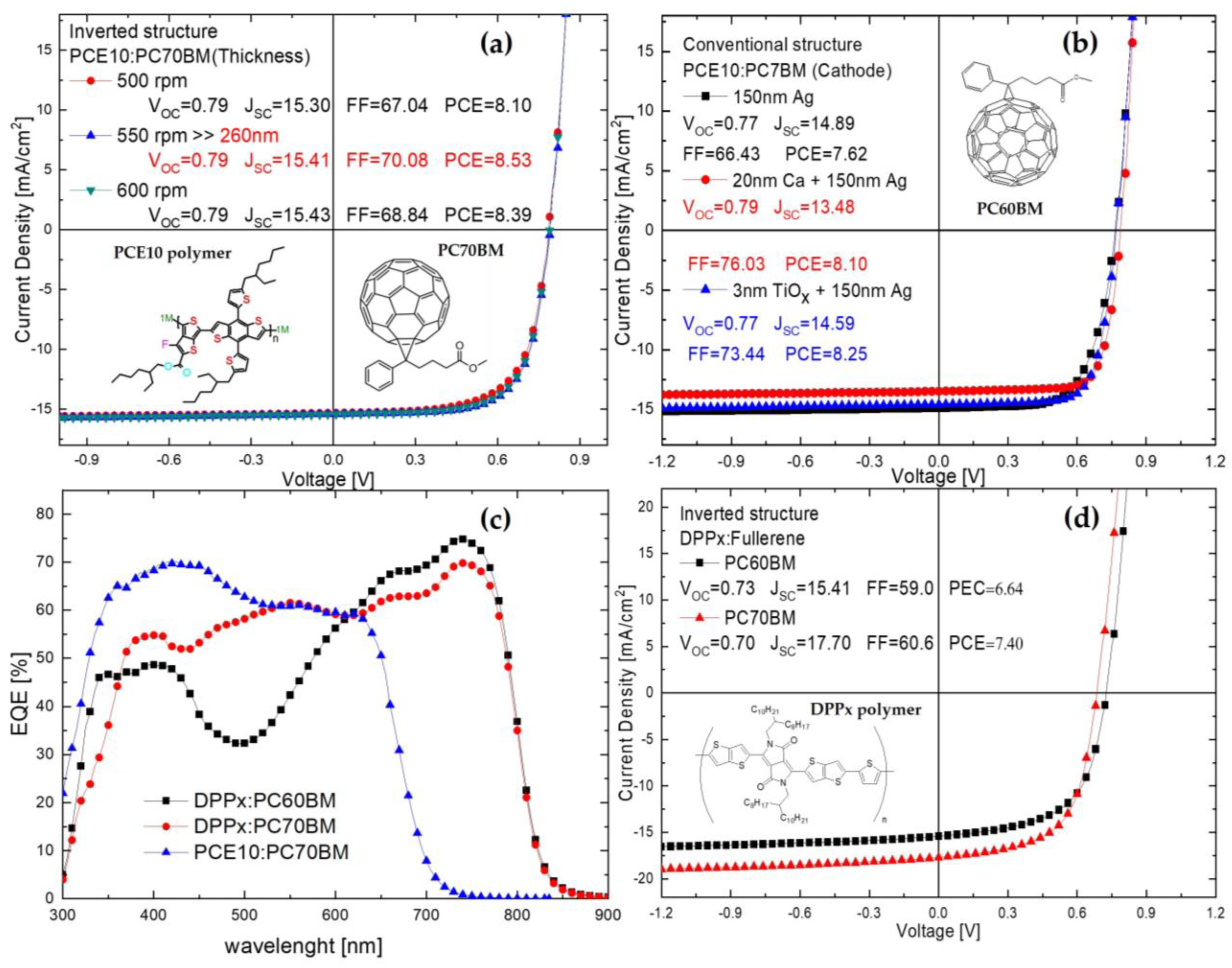
The electrical power generation of an organic solar cell consists of the following steps: light absorption, exciton (electron-hole pairs) generation, exciton dissociation (free electrons and holes), charge transport, and charge extraction [36,37,38,39,40]. One organic active layer can cover only a part of the solar light spectrum. Therefore, a tandem (multi-junction) device built of organic active layers with different absorption spectra can improve the optical absorption of the device and cover a broader range of solar light leading to higher performance than the single junctions (series configuration in the current manuscript). In another case, due to lower charge conductivity of organic materials (high dielectric constant) and as a consequence lower exciton diffusion length, the thickness of the organic active layer is limited. When a single junction device has too thick an active layer, electron-hole pairs (excitons) cannot be dissociated before they recombine with each other; or after exciton dissociation, free electron and hole recombination processes can happen before they can be extracted from the device. Those recombination’s cause an enormous reduction of electrical performance in the solar cell device [41]. Also, here a tandem (multi-junction) device can be used, keeping the same organic material with low (optimum) thickness as the active layer for subcells but having greater total thickness of the whole tandem device compared to the single-junction model. In this way, a tandem device can absorb more sunlight at the same wavelength leading to generation of more photocurrent as a result (parallel configuration in the current manuscript). To build up tandem (multi-junction) photovoltaics, we must first create optimally designed single-junction devices which will be used as subcells. Here, we demonstrate first an opaque inverted device with PCE10:PC70BM active layers with different thicknesses to find the optimum parameters. Then, based on the same parameters, we change the order of buffer layers to create a single-junction device but with conventional structure. Cathode electrodes of 150 nm pure silver layer, 20 nm Calcium (Ca) + 150 nm Ag electrode and 3 nm TiO2 + 150 nm Ag were compared. Pure silver does not have a perfect work-function relative to the LUMO level of the organic active layer to extract the electrons optimally and, therefore, lowers the fill factor (FF). The combination of Ca + Ag has the optimum low work-function properties to have an optimum interface with the LUMO level of the active layer and the highest fill factor (FF) as a result. However, Ca has less optical reflection as top electrode leading to reduction in the light intensity inside the blend and to lower photocurrent (Jsc) generation. The optimum cathode is achieved in a device with conventional configuration when a TiO2 + Ag electrode is used to keep both fill factor (FF) and photocurrent (Jsc) at high values.
In addition, the comparison between inverted and conventional devices with identical organic active and buffer layers shows that the inverted structure leads to higher performance mainly due to higher photocurrent generation (higher Jsc). Therefore, a 2-electrode (2-terminal) series tandem (multi-junction) structure based on two (or more) subcells, all with inverted structures, is recommended. A DPPx:PC70BM single junction with similar inverted structure was used to find the optimum thickness of the active layer film of about 90 nm. The DPPx:PC70BM film absorbs more light compared to DPPx:PC60BM due to the greater absorption of PC70BM compared to PC60BM. Use of PC70BM ensures maximum possible photocurrent generation. For a 3-terminal parallel tandem device, both inverted and conventional configurations must be used since their interconnecting electrode must have the same selectivity (polarity). Here, the middle electrode of the parallel tandem device is the anode to extract and transport holes. In order to justify the choice of combining PCE10:PC70BM and DPPx:PC70BM for subcells of the tandem device, the external quantum efficiencies (EQE) of inverted single-junction devices are also measured, which demonstrates that the polymers have non-overlapping absorption spectra leading to the possibility of increasing the power conversion efficiency (PCE) of single-junction subcells by employing a tandem device structure. This will be demonstrated at the end of the article. Figure 3 demonstrates the electrical and optical properties of subcells to be used at a further stage for tandem (multi-junction) devices.
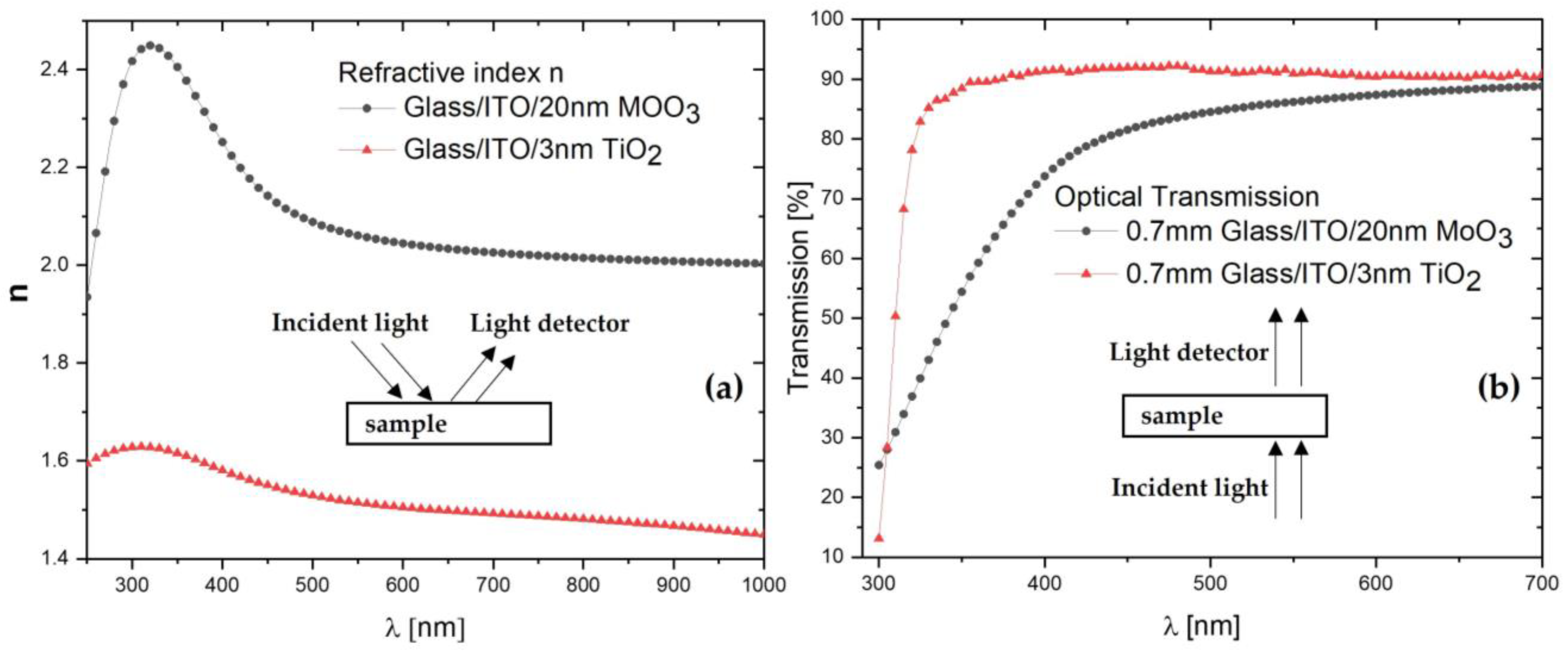
To explain in more detail why a device with inverted structure has higher photocurrent (Jsc) generation compared to the conventional configuration, we must discuss higher intensity of light illuminating the active layer for the inverted cell. Since the glass substrate, both electrodes (ITO and Ag), and the organic active layers are identical in both configurations, the cause of different light intensities inside the device must be the hole (20 nm MoO3) and electron (3 nm TiO2) transport buffer layers. When we apply optical measurements by ellipsometer, we find that both molybdenum oxide (MoO3) and titanium dioxide (TiO2) are optically very transparent, with low k value. However, there is a huge difference between their refractive indexes. The MoO3 layer has a larger refractive index than TiO2 which leads to huge reflection of incident light. The optical transmission of glass/ITO/MoO3 will be limited due to it reflecting the incoming light much more than the glass/ITO/TiO2 sample. Thus, the inverted structure allows more incident light through, leading to higher light intensity inside the active layer and more photocurrent generation (higher Jsc). In addition, due to the high refractive index of MoO3, the opaque top electrode of the inverted structure made of 20 nm MoO3 + 150 nm Ag reflects light back more efficiently to the active layer, causing even higher light intensity inside the organic blend layer. This means that for an inverted device, the cathode electrode (glass/ITO/TiO2) before the active layer is very transparent with low optical reflection properties, while the top metallic anode electrode (MoO3/Ag) is an excellent mirror so that the light intensity inside the device is maximized for the wavelengths where the active layer absorbs the most. The results of ellipsometry measurements, shown in Figure 4, confirm the above reasoning.
Based on single-junction devices previously described, tandem (multi-junction) devices can be generated. The most important challenge to address here is the middle electrode connecting the subcells. For all types of multi-junction, the interconnecting electrode must be protective against chlorinated solvents, avoiding any dissolving of the underlying subcells during the coating of the next subcell. In a series tandem (multi-junction) device, the middle electrode does not have to be conductive at all and it acts only as electron-hole recombination center. Therefore, in this work, a 20 nm MoO3 + 1 nm Ag + 3 nm TiO2 interconnecting electrode is used which is protective and optically very transparent. Such a structure can led to higher performances compared to single-junction subcells by improving the absorption of the device, thus covering a broader range of the solar light spectrum. In contrast, in a parallel tandem (multi-junction) solar cell, the middle electrode must be electrically very conductive (high sheet conductivity) to be able to extract photo-generated charges efficiently. Due to this requirement, a 20 nm MoO3 + 15 nm Ag + 20 nm MoO3 interconnecting layer is used here, due to the lack of a needed sputtering tool for deposition of a more transparent electrode such as ITO. It is a protective electrode but optically is much less transparent due to the presence of a 15 nm silver (Ag) layer. A metallic layer is very absorbing, especially for longer wavelengths. A tandem (multi-junction) device based on a top subcell with maximum absorption at the same region (DPPx polymer in this case) will limit the power conversion efficiency. The multi-junction series and tandem parallel devices are demonstrated in Figure 5. The series tandem device is based on a 150 nm thick PCE10:PC70BM active layer for all subcells showing summation of their open-circuit voltages (Voc). Since all subcells in series multi-junction cells have the same absorption spectra, the efficiency of an optimum single-junction device could not be improved. However, at a later stage, just by changing the active layer of the top cell to DPPx:PC7BM film, an optimum series tandem device is presented. The bottom subcell of the parallel tandem solar cell was made of 190 nm thick PCE10:PC70BM, and the thickness of PCE10:PC70BM of the top sub-cell was varied to find an optimum output. When the active layer of the top subcell is 90 nm thick, an optimum parallel tandem device with total thickness of 280 nm (sum of active layers of bottom and top subcells) is achieved, which has a little more efficiency than an optimum single-junction device based on 260 nm PCE10:PC70BM due to a higher photocurrent (Jsc) and better fill factor (FF).
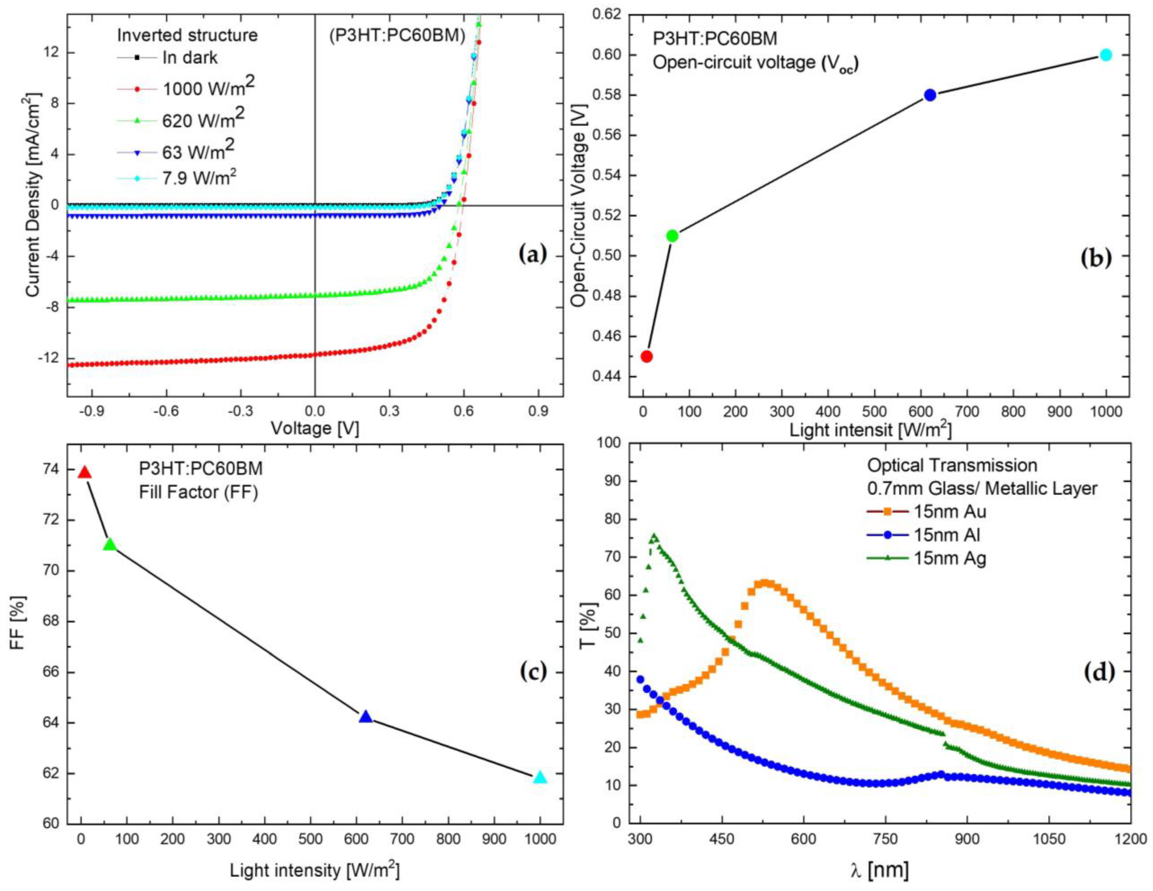
In series multi-junction devices, open-circuit voltages of subcells combine, but note that not each subcell will have the same open-circuit voltage of about Voc = 0.8 Volt as the single-junction device. The higher the number of subcells stacked onto each other, the larger the deviation from the single-junction solar cell’s open-circuit voltage. Only the bottom cell (the first cell) is illuminated with 1 sunlight intensity; the following subcells are illuminated under lower light intensities due to light absorption of the underlying subcells, and therefore their open-circuit voltages will be reduced. With regard to the fill factor of the multi-junction device, the difference in light intensities also plays a role. To explain the measurement results of series tandem (multi-junction) devices shown in Figure 5, it is necessary to address the behavior of organic solar cell fill factor (FF) and open circuit voltage (Voc) under lower light intensities [42]. To do so, a well-known P3HT:PC60BM solar cell was made with inverted structure, using the same configuration as is used in series multi-junction device subcells. The organic layer thickness was 350 nm, and the solar cell was measured under different light intensities by inserting neutral density filters between the solar simulator (Abet) and the device. Figure 6 shows that when the solar cell is illuminated with a lower light intensity, the photo-generated current (Jsc) decreases linearly (Figure 6a), but the fill factor increases (Figure 6c) due to two mechanisms: lower charge carriers lead to less recombination inside the active layer and at the interfaces, and the resistivity of the buffer layers and electrodes are less pronounced because they have to transport lower currents. The 3-fold junction device shows a very high fill factor, larger than both single and tandem devices. However, the 4-fold junction device shows again a reduction of fill factor. We speculate that the light intensity of the last subcell is too low, and in practical terms acts as an additional resistor which increases the series resistance of the whole device causing lowering of the fill factor (FF). The open-circuit voltage (Voc) of the solar cell also decreases under lower light intensity conditions (Figure 6b) [43,44]. This effect is in harmony with observations of voltages of multi-junction devices. To provide more insight into the optical properties of the middle electrode of the parallel tandem device, the optical transmissions of 15 nm metallic electrodes (Au, Ag, and Al) are shown in Figure 6. The absorption properties of those typically used electrodes, especially for longer wavelengths, provides motivation to use transparent conductive electrodes, such as ITO, for more optimized and higher-performance devices.
An optical simulation was performed, as demonstrated in Figure 7a,b, to find the optimum region of bandgaps for active layers of subcells of a tandem device for both series and parallel configurations. These simulations represent the upper limit with modest assumptions regarding individual cell performance ((Voc = Eg − 0.6 eV)/e, EQE = 65%, IQE = 85%, and FF = 65%). Figure 7a,b shows the maximum theoretically achievable efficiencies for tandem cells connected in either series or parallel as a function of the bandgap of the active materials used for the front and back cell. Note that we assumed a very transparent middle electrode for both series and parallel configurations during the simulations. The maximum achievable efficiency is around 15% for a series combination of materials strictly restricted to the darkest red area in Figure 7a,b (1.4 eV < Eg subcell 1 < 1.7 eV; 1.1 eV < Eg subcell 2 < 1.5 eV). The optimum bandgap of the front cell should be between 1.4 and 1.7 eV, while the bandgap of the back cell should be between 1.1 and 1.5 eV (best for Eg subcell 1 = 1.66 eV; Eg subcell 2 = 1.33 eV). For this work, commercially available PCE10 and DPPx polymers were used. Before attempting the fabrication of tandem cells with varying thickness of the photoactive films for the front and the back cell, we combined an electrical and optical model in order to be able to predict the best layer thickness for the highest performance in a tandem cell based on the real performance of each single cell with inverted structures, since they show a higher performance over conventional polarity. The transparent ITO electrode is used for electron extraction by applying 3 nm solution-processed TiO2 as the interlayer. Followed by the photoactive layer, the device is finished with a top contact of 20 nm MoO3 and 150 nm Ag. Figure 7c,d shows that the experimental work and device measurements under 1 sun illumination are in harmony with theoretical simulations showing that thicknesses of 160 nm PCE10:PC70BM film for the bottom cell and 90 nm DPPx:PC70BM layer for the top cell are optimum values leading to maximum performance of PCE = 10.6%, which is higher than all performances of all types of single-junction devices presented in this work.
It is important to note that the previous models used to calculate the maximum achievable efficiency as a function of the bandgap of both active films predicted a PCE for this combination of materials of around 15%. These numbers are well above the efficiencies reported for single cells here, thus the effort to attempt tandem is justified. However, the combination of the electrical and optical model predicts a maximum efficiency of 11%, providing the optimum thickness for each case. The latter refers to a more realistic situation, since the former assumes an FF and a constant EQE of 65% which, as we have seen, is not always strictly achievable in single experimental devices, and even more difficult when they are implemented in tandem.
4. Conclusions
Buffer layers made of metal oxides can provide the necessary properties to generate single- and multi-junction solution-processed organic solar cells. Titanium dioxide (TiO2) dispersion processed at room temperature as an electron transport layer can be readily utilized for all types of devices with different configurations. The thermally evaporated molybdenum oxide layer (MoO3) as hole transporting layer was mechanically dense (closed layer) and chemically stable enough to protect the subcells during solution processing of the active layer precursor with chlorinated solvents. They provide well-matched electrical energy levels leading to proper selectivity of the electrode and good protection properties. This result was possible only by paying close attention to details such as controlling the temperature and moisture conditions for TiO2 dispersion or deposition steps, such as a very low evaporation rate and using a crucible for deposition of thermally evaporated MoO3. A single-junction organic solar cell with inverted structure has higher performance mainly due to higher photocurrent generation caused by the highly transparent bottom and highly reflecting top metallic electrode. For high performance tandem (multi-junction) solar cells, the interconnecting electrode must be very transparent and active layers of subcells must have non-overlapping absorption spectra. By combining optical and electrical simulations with a lot of experimental effort, an optimized series tandem device is presented with high performance of PCE = 10.6%, which was more efficient than all single-junction structures. The limited performance reported here, compared to recent higher efficiencies in the literature, was due to the lack of optimized state-of-the-art organic materials. By utilizing identical device structures to those reported here, and better donors and acceptors, much higher performances can be achieved. To make the parallel tandem structure as efficient as the series configuration, a conductive but transparent electrode such as ITO has to be used instead of metallic layers. Note that, besides power conversion improvements, the high stability (long lifetime) is a very important issue to consider for commercializing such a technology.
Funding
This research received no external funding.
Institutional Review Board Statement
Not applicable.
Informed Consent Statement
Not applicable.
Data Availability Statement
The data presented in this study are available on request from the corresponding author.
Acknowledgments
The author acknowledges Inter Molecular Electronic Center (IMEC/Belgium) and Kuwait Foundation for the Advancement of Sciences (KFAS) for technical and financing support, respectively. The author acknowledges Dr. Rober Gehlhaar for simulation results.
Conflicts of Interest
The author declares no conflicts of interest.
References
- Guo, C.D.; Li, L.; Wang, B.; Du, Z.-X.; Liu, Z.; Shen, P.; Wang, X.; Zhang, J.; Cai, S.; Cheng, C.; et al. Cold-Aging and Solvent Vapor Mediated Aggregation Control toward 18% Efficiency Binary Organic Solar Cells. Adv. Energy Mater. 2021, 11, 2102000. [Google Scholar] [CrossRef]
- Li, C.; Zhou, J.; Song, J.; Xu, J.; Zhang, H.; Zhang, X.; Guo, J.; Zhu, L.; Wei, D.; Han, G.; et al. Non-fullerene acceptors with branched side chains and improved molecular packing to exceed 18% efficiency in organic solar cells. Nat. Energy 2021, 6, 605–613. [Google Scholar] [CrossRef]
- Cai, Y.; Li, Y.; Wang, R.; Wu, H.; Chen, Z.; Zhang, J.; Ma, Z.; Hao, X.; Zhao, Y.; Zhang, C.; et al. A well-mixed phase formed by two compatible non-fullerene acceptors enables ternary organic solar cells with efficiency over 18.6%. Adv. Mater. 2021, 33, 2101733. [Google Scholar] [CrossRef] [PubMed]
- Bi, P.; Zhang, S.; Chen, Z.; Xu, Y.; Cui, Y.; Zhang, T.; Ren, J.; Qin, J.; Hong, L.; Hao, X.; et al. Reduced non-radiative charge recombination enables organic photovoltaic cell approaching 19% efficiency. Joule 2021, 5, 2408–2419. [Google Scholar] [CrossRef]
- Khandelwal, K.; Biswas, S.; Mishra, A.; Ganesh, D.; Sharma, G.D. Semitransparent organic solar cells: From molecular design to structure–performancerelationships. J. Mater. Chem. C 2022, 10, 13. [Google Scholar] [CrossRef]
- Ballif, C.; Perret-Aebi, L.; Lufkin, S.; Rey, E. Integrated thinking for photovoltaics in buildings. Nat. Energy 2018, 3, 438–442. [Google Scholar] [CrossRef]
- Mishra, A.; Bauerle, P. Small molecule organic semiconductors on the move. Angew. Chem. Int. Ed. 2012, 51, 2020–2067. [Google Scholar] [CrossRef] [PubMed]
- Mishra, A. Material perceptions and advances in molecular heteroacenes for organic solar cells. Energy Environ. Sci. 2020, 13, 4738–4793. [Google Scholar] [CrossRef]
- Jiang, Y.; Bai, Y.; Wang, S. Orgaic solar cells: From fundamental to application. Energies 2023, 16, 2262. [Google Scholar] [CrossRef]
- Cui, Y.; Hong, L.; Hou, J. Organic photovoltaics cells for indoor applications: Opportunities and challenges. Appl. Mater. Interfaces 2020, 12, 38815–38828. [Google Scholar] [CrossRef]
- Fukuda, K.; Yu, K.; Someya, T. The future of flexible organic solar cells. Adv. Energy Mater. 2020, 10, 2000765. [Google Scholar] [CrossRef]
- Xu, X.; Yu, L.; Peng, Q. Recent advances in wide bandgap polymer donors and their applications in organic solar cells. Chin. J. Chem. 2021, 39, 243–254. [Google Scholar] [CrossRef]
- Suman Banerjee, S.; Gupta, S.K.; Singh, A.; Garg, A. Buffer layers in inverted organic solar cells and their impact on the interface and device characteristics: An experimental and modeling analysis. Org. Electron. 2016, 37, 228–238. [Google Scholar] [CrossRef]
- Bishnoi, S.; Datt, R.; Arya, S.; Gupta, S.; Gupta, R.; Chung Tsoi, W.; Sharma, S.N.; Patole, S.P.; Gupta, V. Engineered Cathode Buffer Layers for Highly Efficient Organic Solar Cells: A Review. Adv. Mater. Interfaces 2022, 9, 2101693. [Google Scholar] [CrossRef]
- Sreejith, S.; Ajayan, J.; Uma Reddy, N.V.; Manikandan, M.; Radhika, J.M. Critical Review on Various Buffer Layers used to Enhance the Photovoltaic Performance of Organic Solar Cells. Curr. Nanosci. 2023, 20, 801–819. [Google Scholar] [CrossRef]
- Mihailtchi, V.D.; Blom, P.W.M.; Hummelen, J.C.; Janssen, R.A.J.; Kroon, J.M.; Rispens, M.T. Cathode dependence of the open-circuit voltage of polymer-fullerene bulk heterojunction solar cells. J. Appl. Phys. 2003, 94, 6849. [Google Scholar] [CrossRef]
- Mihailtchi, V.D.; Koster, L.J.A.; Blom, P.W.M. Effect of metal electrodes on the performance of polymer-fullerene bulk heterojunction solar cells. Appl. Phys. Lett. 2004, 85, 970. [Google Scholar] [CrossRef]
- Hadipour, A.; De Boer, B.; Wildeman, J.; Kooistra, F.B.; Hummelen, J.C.; Turbiez, M.G.R.; Wienk, M.M.; Janssen, R.A.J.; Blom, P.W.M. Solution-processed Organic Tandem Solar Cells. Adv. Funct. Mater. 2006, 16, 1897–1903. [Google Scholar] [CrossRef]
- Hadipour, A.; De Boer, B.; Blom, B.P.W. Solution-processed Organic Tandem Solar Cells with Imbedded Optical Spacers. J. Appl. Phys. 2007, 102, 074506. [Google Scholar] [CrossRef]
- Hadipour, A.; de Boer, B.; Blom, P.W.M. Organic Tandem and Multi-Junction Solar Cells. Adv. Funct. Mater. 2008, 18, 169–181. [Google Scholar] [CrossRef]
- Zheng, Z.; Wang, J.; Bi, P.; Ren, J.; Wang, Y.; Yang, Y.; Liu, X.; Zhang, S.; Hou, J. Tandem Organic Solar Cell with 20.2% Efficiency. Joule 2022, 6, 171–184. [Google Scholar] [CrossRef]
- Sha Liu, S.H.; Yuan, J.; Deng, W.; Luo, M.; Xie, Y.; Liang, Q.; Zou, Y.; He, Z.; Wu, H.; Cao, Y. High-efficiency organic solar cells with low non-radiative recombination loss and low energetic disorder. Nat. Photonics 2020, 14, 300–305. [Google Scholar]
- Elumalai, N.K.; Uddin, A. Open circuit voltage of organic solar cells: An in-depth review. Energy Environ. Sci. 2016, 9, 391–410. [Google Scholar] [CrossRef]
- Hadipour, A.; De Boer, B.; Blom, P.W.M. Device Operation of Organic Tandem Solar Cells. Org. Electron. 2008, 9, 617–624. [Google Scholar] [CrossRef]
- Sergeant, N.P.; Hadipour, A.; Niesen, B.; Cheyns, D.; Heremans, P.; Peumans, P.; Rand, B.P. Design of Transparent Anodes for Resonant Cavity Enhanced Light Harvesting in Organic Solar Cells. Adv. Mater. 2012, 24, 728–732. [Google Scholar] [CrossRef] [PubMed]
- Hadipour, A.; Cheyns, D.; Rand, B.P.; Heremans, P. Electrode Considerations for the Optical Enhancement of Organic Bulk Heterojunction Solar cells. Adv. Energy Mater. 2011, 1, 930–935. [Google Scholar] [CrossRef]
- Wang, Y.; Bai, H.; Zhan, X. Comparison of conventional and inverted structures in fullerene-free organic solar cells. J. Energy Chem. 2015, 24, 744–749. [Google Scholar] [CrossRef]
- Salim, M.B.; Nekovei, R.; Jeyakumar, R. Oragnic tandem solar cells with 18.6% efficiency. Sol. Energy 2020, 198, 160–166. [Google Scholar] [CrossRef]
- Li, M.; Gao, K.; Wan, X.; Zhang, Q.; Kan, B.; Xia, R.; Liu, F. Solution-processed organic tandem solar cells with power conversion efficiency > 12%. Nat. Photonics 2017, 11, 85–90. [Google Scholar] [CrossRef]
- Ullah, F.; Chen, C.C.; Choy, W.C.H. Recent developments in organic tandem solar cells toward high efficiency. Adv. Energy Sustain. Res. 2021, 2, 2000050. [Google Scholar] [CrossRef]
- Meng, L.; Zhang, Y.; Wan, X.; Li, C.; Zhang, X.; Wang, Y.; Ke, X. Organic and solution-processed tandem solar cells with 17.3% efficiency. Science 2018, 361, 1094–1098. [Google Scholar] [CrossRef]
- Zuo, L.; Yu, J.; Shi, X.; Lin, F.; Tang, W. High-efficiency nonfullerene organic solar cells with a parallel tandem configuration. Adv. Mater. 2017, 29, 1702547. [Google Scholar] [CrossRef]
- Hadipour, A.; Muller, R.; Heremans, P. Room Temperature Solution-processed electron transport layer for organic solar cells. Org. Electron. 2013, 14, 2379–2386. [Google Scholar] [CrossRef]
- Chen, G.; Ling, Z.; Wei, B.; Zhang, J.; Hong, Z.; Sasabe, H.; Kido, J. Comparison of the solution and vacuum-processed Squaraine:Fullerene small molecule bulk heterojunction solar cells. Front. Chem. 2018, 6, 412. [Google Scholar] [CrossRef]
- Pan, T.; Li, J.; Lin, Y.; Zue, Z.; Di, Z.; Yin, M.; Wang, J.; Lu, L.; Yang, L.; Li, D. Structural and optical studies of molybdenum oxides thin films obtained by thermal evaporation and atomic layer deposition methods for photovoltaic application. J. Mater. Sci. Mater. Electron. 2021, 32, 3475–3486. [Google Scholar] [CrossRef]
- Blom, P.W.M.; Woudenberh, T.; Tanase, C.; Mihailtchi, V.D.; de Boer, B. Charge transport in polymeric opto-electronic devices. Polym. Prepr. 2003, 44, 342. [Google Scholar]
- Mihailtchi, V.D.; Koster, L.J.A.; Hummelen, J.C.; Blom, P.W.M. Photocurrent generation in polymer-fullerene bulk heterojunctions. Phys. Rev. Lett. 2004, 93, 216601. [Google Scholar] [CrossRef]
- Koster, L.J.A.; Mihailtchi, V.D.; Blom, P.W.M. Extraction of photogenerated charge carriers from polymer-fullerene bulk heterojunction solar cells. Proc. SPIE 2004, 5464, 239. [Google Scholar]
- Mihailtchi, V.D.; Wildeman, J.; Blom, P.W.M. Space-charge limited photocurrent. Phys. Rev. Lett. 2005, 94, 126602. [Google Scholar] [CrossRef]
- Koster, L.J.A.; Smits, E.C.P.; Mihailtchi, V.D.; Blom, P.W.M. Device model for the operation of polymer-fullerene bulk heterojunction solar cells. Phys. Rev. B 2005, 72, 085205. [Google Scholar] [CrossRef]
- Koster, L.J.A.; Mehailtchi, V.D.; Blom, P.W.M. Biomolecular recombination in polymer-fullerene bulk heterojunction solar cells. Appl. Phys. Lett. 2006, 88, 052104. [Google Scholar] [CrossRef]
- Ryu, S.; Ha, N.Y.; Ahn, Y.H.; Park, J.; Lee, S. Light intensity dependence of organic solar cell operation and dominance switching between Shockley–Read–Hall and bimolecular recombination losses. Sci. Rep. 2021, 11, 16781. [Google Scholar] [CrossRef] [PubMed]
- Koster, L.J.A.; Mihailtchi, V.D.; Ramaker, R.; Xie, H.; Blom, P.W.M. Light intensity dependence of open-circuit voltage of polymer-fullerene solar cells. Appl. Phys. Lett. 2005, 86, 123509. [Google Scholar] [CrossRef]
- Koster, L.J.A.; Mihailtchi, V.D.; Xie, H.; Blom, P.W.M. Origin of the light intensity dependence of the short-circuit current of polymer-fullerene solar cells. Appl. Phys. Lett. 2005, 87, 203502. [Google Scholar] [CrossRef]
Figure 1.
Device structures of (a): inverted and (b) conventional single-junction polymer: fullerene solar cells are shown.
Figure 1.
Device structures of (a): inverted and (b) conventional single-junction polymer: fullerene solar cells are shown.

Figure 2.
Device structures of (a): parallel and (b) series tandem polymer: fullerene solar cells are shown.
Figure 2.
Device structures of (a): parallel and (b) series tandem polymer: fullerene solar cells are shown.

Figure 3.
(a) Single junction opaque device with inverted structure based on PCE10:PC70BM blend with different thicknesses demonstrating optimum thickness of 260 nm, (b): single junction opaque device with conventional structure demonstrating different cathode combinations, (c) external quantum efficiency (EQE) of the inverted devices with PCE10:PC70, DPPx:PC70BM, and DPPx:PC60BM active layers, (d) single junction opaque inverted device based on 90 nm DPPx:PC70BM or DPPx:PC60BM. Insets show the chemical structures of materials used in the active layer.

Figure 4.
(a) Ellipsometry data demonstrating the refractive indexes (n) of both buffer layers, (b) optical transmission of substrate with transparent electrode ITO and both buffer layers are demonstrated. It is clear that the high refractive index of the MoO3 layer leads to lower optical transmission causing lower light intensity within the device with conventional structure compared to the inverted configuration.

Figure 5.
(a) Series multi-junction devices all based on 150 nm PCE10:PC70BM organic active layer, demonstrating the capability of the metal oxide-based device structure and proper summation of open-circuit voltages of subcells, (b) parallel tandem device based on 190 nm thick PCE10:PC70BM film and the same active layer material of the top subcell but with different thicknesses demonstrating improved short-circuit current and higher power conversion efficiency than a single-junction device when 90 nm thick PCE10:PC70BM is used.

Figure 6.
(a) Current/Voltage (JV) characteristics of a single-junction P3HT:PC60BM solar cell under different light intensities showing linear reduction of photo-generated current (Jsc), (b) non-linear behavior in reduction of open-circuit voltage (Voc) for lower light intensity, (c) increase in fill factor at lower illumination intensities, (d) optical absorption of 15 nm metallic electrodes.

Figure 7.
Power conversion efficiency as a function of the bandgap of the absorbing materials used for the front (Eg subcell 1) and back (Eg subcell 2) cell in (a) 2-terminal series connection and (b) 3-terminal parallel connection, (c) by assuming that each absorbed photon is contributing to the current density (charge collection efficiency = 1), the tandem efficiency is calculated considering determined charge collection efficiencies, measured single cell open circuit voltages, and a realistic fill factor, (d) the current-voltage measurements of semitransparent inverted PCE10:PC70BM (160 nm thick) bottom cell, inverted opaque DPPx:PC70BM (90 nm thick) top cell, and 2-terminal tandem device are demonstrated under 1 sun illumination intensity.

Disclaimer/Publisher’s Note: The statements, opinions and data contained in all publications are solely those of the individual author(s) and contributor(s) and not of MDPI and/or the editor(s). MDPI and/or the editor(s) disclaim responsibility for any injury to people or property resulting from any ideas, methods, instructions or products referred to in the content. |
© 2024 by the author. Licensee MDPI, Basel, Switzerland. This article is an open access article distributed under the terms and conditions of the Creative Commons Attribution (CC BY) license (https://creativecommons.org/licenses/by/4.0/).
Share and Cite
MDPI and ACS Style
Hadipour, A. Utilizing Metal Oxide Thin Films for Device Engineering of Solution-Processed Organic Multi-Junction Solar Cells. Coatings 2024, 14, 525. https://doi.org/10.3390/coatings14050525
AMA Style
Hadipour A. Utilizing Metal Oxide Thin Films for Device Engineering of Solution-Processed Organic Multi-Junction Solar Cells. Coatings. 2024; 14(5):525. https://doi.org/10.3390/coatings14050525
Chicago/Turabian StyleHadipour, Afshin. 2024. "Utilizing Metal Oxide Thin Films for Device Engineering of Solution-Processed Organic Multi-Junction Solar Cells" Coatings 14, no. 5: 525. https://doi.org/10.3390/coatings14050525
Note that from the first issue of 2016, this journal uses article numbers instead of page numbers. See further details here.