Growth without Postannealing of Monoclinic VO2 Thin Film by Atomic Layer Deposition Using VCl4 as Precursor


Department of Applied Physics, National Pingtung University, Pingtung 90003, Taiwan
*
Author to whom correspondence should be addressed.
Coatings 2018, 8(12), 431; https://doi.org/10.3390/coatings8120431
Submission received: 18 October 2018
/
Revised: 17 November 2018
/
Accepted: 26 November 2018
/
Published: 27 November 2018
(This article belongs to the Special Issue Atomic Layer Deposition)
Abstract
:Vanadium dioxide (VO2) is a multifunctional material with semiconductor-to-metal transition (SMT) property. Organic vanadium compounds are usually employed as ALD precursors to grow VO2 films. However, the as-deposited films are reported to have amorphous structure with no significant SMT property, therefore a postannealing process is necessary for converting the amorphous VO2 to crystalline VO2. In this study, an inorganic vanadium tetrachloride (VCl4) is used as an ALD precursor for the first time to grow VO2 films. The VO2 film is directly crystallized and grown on the substrate without any postannealing process. The VO2 film displays significant SMT behavior, which is verified by temperature-dependent Raman spectrometer and four-point-probing system. The results demonstrate that the VCl4 is suitably employed as a new ALD precursor to grow crystallized VO2 films. It can be reasonably imagined that the VCl4 can also be used to grow various directly crystallized vanadium oxides by controlling the ALD-process parameters.
1. Introduction
Vanadium dioxide (VO2) has attracted extensive research interest during the past decades owing to its unique behavior, called semiconductor-to-metal transition (SMT) or insulator-to-metal transition (IMT), which accompanies the reversible and ultrafast phase transition between monoclinic VO2 [VO2(M)] and tetragonal rutile VO2 [VO2(R)] at temperatures around 340 K (~67 °C) [1,2,3,4,5]. Thus, the optical and electrical properties of VO2 can be switched by controlling the SMT behavior of VO2 [6,7]. Numerous factors for adjusting the SMT behavior of VO2 have already been established that include impurity doping [8], stoichiometry [9], strain [10], grain boundary [11], oxygen vacancy [12], applied external electrical field [13], and light irradiation [14]. Therefore, the VO2 has been widely investigated as a key material for applications in the smart thermochromic windows [15], two-terminal electronic devices [16], electric-field-effect three-terminal devices [17,18], integrated optical circuits [19], electronic oscillators [20], metamaterials [21], memristive devices [22], programmable critical thermal sensors [23], gas sensors [24], and so forth.
Various techniques had been employed for preparing VO2 films, including the sol–gel method [22,23], electron-beam evaporation [25,26], sputtering [5,17], pulsed laser deposition (PLD) [27,28], molecular beam epitaxy (MBE) [16,29], chemical vapor deposition (CVD) [30,31,32,33,34], and atomic layer deposition (ALD) [35,36,37,38,39,40,41,42,43,44,45,46,47,48,49,50]. Among them, ALD is an excellent technique which has drawn much attention due to its many advantages, including preparation of the highly conformal thin films with almost 100% step coverage, accurate control of film thickness at the atomic scale, low growth temperature, and wide-area uniformity. These features make ALD a powerful technique for the fabrication of emerging nanostructures and nanodevices [51,52,53].
Generally, organic vanadium compounds are employed as ALD precursors and reacted with H2O or O3 to grow vanadium oxide thin films, such as tetrakis(ethylmethylamino)vanadium (TEMAV) [35,36,37,38,39,40,41,42], vanadyl isopropoxide (VTIP) [43,44,45,46], and vanadyl triisopropoxide (VTOP) [47,48,49,50]. However, the organic precursors (TEMAV, VTIP, and VTOP) are only suitable for low process temperatures in ALD because the decomposition temperatures of TEMAV, VTIP, and VTOP are about 175 [35,40], 200 [43], and 180 °C [49,50], respectively. When the process temperature is higher than the decomposition temperature of the precursor, the growth mechanism of film will be changed from ALD to CVD-like mode [35,40,43,49,50]. In this case, the film is grown by CVD instead of ALD. This is why the low temperature of 120–170 °C is usually used for the film growth of ALD using TEMAV, VTIP, or VTOP as precursor. However, the low process temperature is not enough to grow crystalline films. Therefore, the as-deposited vanadium oxide films grown by ALD from organic vanadium precursors are generally reported to have amorphous structures with no significant SMT behavior and a postannealing process is necessary for converting the amorphous to crystalline VO2. Previous studies have reported that postannealing in N2, He, O2, or N2/O2 mixed gas with a low O2 partial pressure resulted in crystalline monoclinic VO2 for the temperature range of 425–585 °C [35,36,37,38,39,40,41,42]. Since the extra postannealing process is necessary to obtain a crystalline VO2, it results in higher manufacturing costs and increases the failure possibilities of the process and products.
This work reports that a directly crystalline VO2 film has been successfully grown by ALD using vanadium tetrachloride (VCl4) and H2O as precursors at a reaction temperature of 350 °C without any postannealing process. It is noticed that the inorganic VCl4 is used as an ALD precursor for the first time, although a few papers reported that the VCl4 had been used in traditional chemical vapor deposition (CVD) techniques [30,31,32]. The VO2 film has a significant SMT behavior with a VO2(M)-to-VO2(R) phase-transition temperature of about 61 ± 1 °C, which is verified from temperature-dependent Raman spectra and sheet-resistance variations of VO2 film. Besides, the VO2 film exhibits two orders of magnitude change in sheet resistance across the semiconductor-to-metal transition although the film thickness is only 30 nm. The results demonstrated that crystalline VO2 films can be directly grown by ALD using VCl4 and H2O as precursors without any postannealing process, presenting a new selection of precursors for the ALD process to grow the crystalline VO2 films.
2. Materials and Methods
In this work, VO2 films were grown on native silicon-oxide-covered Si (100) substrates by ALD at 350 °C with 1000 reaction cycles. VCl4 and H2O were employed as precursors to grow the VO2 films, and Ar was used as purge gas. The reservoirs of the VCl4 and H2O precursors were kept at the temperatures of 30 and 25 °C, respectively. The dosing rates of VCl4 and H2O were 0.288 and 0.296 cc/pulse, respectively, as determined by the reservoir temperature and vapor injection time. The flow rate of Ar was 5 sccm, as controlled by a mass flow controller (MFC, SEC-4400M, HORIBA STEC, Kyoto, Japan). An eight-step sequence of gas injection was applied in an ALD cycle, as combined four conventional gas-injection steps and four additional pump-down steps. The pump-down steps can effectively evacuate excess precursors and byproducts to obtain high-quality films with low Cl impurity contents and ensure the achievement of “true ALD mode” growth [54,55]. The time for each step in an ALD cycle was 0.1, 1, 0.5, 1, 0.5, 1, 0.5, and 1 s for VCl4 vapor injection, pump-down, Ar purge, pump-down, H2O vapor injection, pump-down, Ar purge, and pump-down, respectively.
The crystalline structures of the VO2 films were examined by an X-ray diffractometer (XRD, D8 Advance Eco, Bruker, Karlsruhe, Germany) at 30 and 90 °C. The surface morphologies of the film were observed with a high-resolution scanning electron microscope (SEM, SU8000, Hitachi, Tokyo, Japan). In addition, in order to obtain real surface morphology of the film, the SEM analysis was performed without any conductive coating on the VO2 film surface. The cross-sectional microstructures of the VO2 films were observed by a high-resolution transmission electron microscope (TEM, JEM-2100F, JEOL, Tokyo, Japan). The film thickness was measured from the cross-sectional TEM micrograph and the growth rate of the VO2 film was estimated from an equation of “growth rate = (film thickness/numbers of ALD cycles)”. The chemical composition of the VO2 film was analyzed by a high-resolution X-ray photoelectron spectrometer (XPS, Quantera SXM, ULVAC-PHI, Chigasaki, Japan). In addition, the XPS analysis was performed on the VO2 film surface before and after Ar ion etching with an etching depth of about 2 nm. The temperature-dependent Raman spectra of the VO2 film were examined at temperatures between 30 and 80 °C by a micro Raman spectrometer (Raman, UniRAM II, Uninanotech, Yongin, Korea) with a temperature-controllable sample stage. The temperature-dependent sheet resistance of the VO2 film was measured at temperatures between 30 and 90 °C by a Keithley 2614B SourceMeter (Keithley, Solon, OH, USA) under a four-point probing configuration with a temperature-controllable sample stage.
3. Results and Discussion
Figure 1 shows the XRD patterns of VO2 film measured at 30 and 90 °C, which demonstrate the structural transition of VO2 film from monoclinic (30 °C) to tetragonal rutile (90 °C) phase. The VO2 film measured at 30 °C (Figure 1a) displays that two XRD peaks located at 2θ of 27.9° and 55.4° can be indexed to the (011) and (220) planes of monoclinic VO2(M) (JCPDS no.: 82–0661), respectively. When the temperature is raised to 90 °C (Figure 1b), two XRD peaks located at 2θ of 27.6° and 55.4° are detected, which can be assigned to the (110) and (211) planes of tetragonal rutile VO2(R) (JCPDS no.: 79–1655), respectively. In addition, because the VO2 film is grown on Si substrate, an obvious XRD peak of Si (113) at 2θ of 51.9° has also been detected (Supplementary materials: Part 1). Figure 1c is a comparison of Figure 1a,b, which clearly shows an XRD peak shift of VO2(M) (011) to VO2(R) (110) peak in 26° ≤ 2θ ≤ 30° and the XRD peak of Si substrate does not shift. The XRD peak-shifting behavior is a diagnostic feature for the phase transition of VO2 film from monoclinic to tetragonal rutile structure. Previously, the similar XRD peak-shifting phenomenon had also been reported by Wu et al. [56] for confirming the phase transformation of monoclinic VO2 to tetragonal rutile VO2.
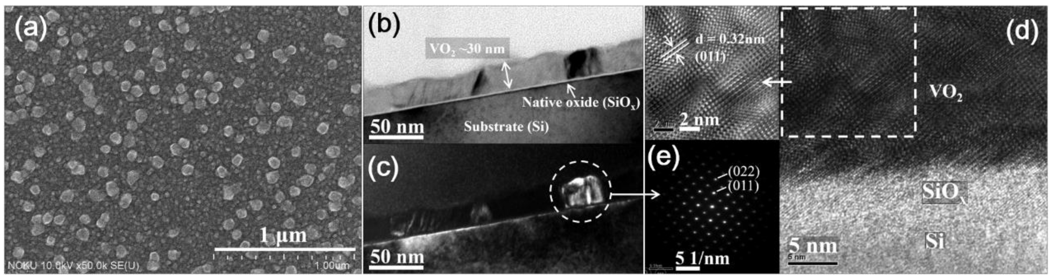
Figure 2 shows the SEM and TEM analyzed results for surface and cross-sectional microstructures of the VO2 film, respectively. The SEM image of surface morphology of the VO2 film (Figure 2a) displays a conformal VO2 film with bigger grains surrounded by small grains; the grain sizes of big and small grains are about 78 ± 14 and 40 ± 6 nm, respectively. According to the cross-sectional TEM bright-field and dark-field images (Figure 2b,c), it can be clearly observed that the VO2 film is grown on a native oxide layer (SiOx) of Si substrate and constructed from columnar grains. The thickness of the VO2 film is about 30 nm, and displays its growth rate at about 0.03 nm/cycle. Moreover, the VO2 grains are directly crystallized and grown on the top surface of the native oxide layer, which is verified by the high-resolution TEM (HR-TEM) image of the VO2/SiOx/Si interface (Figure 2d). The HR-TEM image also reveals a clear lattice fringe of about 0.32 nm, corresponding to the (011) plane of VO2(M). The selected-area electron-beam diffraction (SA-EBD) pattern obtained by focusing the electron beam on an individual VO2 grain is shown in Figure 2e; the SA-EBD pattern can be indexed to monoclinic VO2(M) in agreement with the XRD results.
Figure 3 shows the V2p, O1s, and Cl2p XPS spectra for original (before etching) and after argon-ion etching surface of VO2 film. In addition, the chemical composition of VO2 film calculated from XPS spectra are shown in Table 1. The V and O concentrations of VO2 film are about 25.7 at.% and 74.3 at.%, respectively, for the film before surface etching and are about 33.1 at.% and 66.9 at.%, respectively, for the film after surface etching. The results clearly indicate that the original surface of the VO2 film has a higher oxygen concentration because the VO2 film was exposed to air (oxygen-rich) environment, resulting in absorption of oxygen and a native oxide layer (overoxidation layer) forming on the surface of the VO2 film [26,33,34,39,41,43,57,58]. After argon-ion etching, surface contamination and the native oxide layer of the VO2 film had been removed, and the atomic proportion of V:O atom was about 1:2 in agreement with the stoichiometry of VO2. Besides, no Cl impurity had been detected in the VO2 film, demonstrating the Cl concentration in the VO2 film was lower than the detection limit of XPS (approximately 0.1 at.%). It is noteworthy that this work successfully achieved VO2 film with high purity (Cl impurity <0.1 at.%) by using a low growth temperature of 350 °C, which can be attributed to the additional pump-down steps in the ALD reaction cycles effectively evacuating excess precursors and byproducts [54]. In a previous study, Cheng et al. reported that implementation of pump-down steps into the gaseous-pulse cycle of ALD can effectively reduce the Cl residues. They used TiCl4 as ALD precursor to grow TiN films by using conventional four-step ALD and modified six-step ALD (adding two pump-down steps). Their results showed that the Cl residues of TiN films can be decreased from about 7.7 at.% to 2.3 at.% at the growth temperature of 300 °C [54].
In Figure 3a, the V2p3/2 peak of the original VO2 film (before surface etching) can be fitted with two peaks at binding energy of about 517.2 and 515.6 eV, which can be assigned to V5+ and V4+, respectively [26,33,34,39,41,43,57,58]. Musschoot et al. [43] and Sliversmit et al. [57] reported that the V5+ signal is mainly contributed from the native oxide layer (overoxidation layer) of VO2 film. After surface etching (to remove the native oxide layer), the V2p3/2 peak has a maximum at 515.6 eV (assigned to V4+), which primarily confirms VO2 stoichiometry. In Figure 3b, the O1s XPS peaks are located at binding energy of about 529.8 and 530.5 eV for the original and after-surface-etching VO2 film, showing a peak-shifting phenomenon. The similar peak-shifting phenomenon of O1s XPS peak for VO2 film after surface etching by argon ion sputtering had also been observed by Musschoot et al. [43].
Figure 4a,b show the selected temperature-dependent Raman spectra of the VO2 film for heating and cooling cycles, respectively. It is noticed that the full temperature-dependent Raman spectra of the VO2 films for temperatures between 30 and 80 °C in heating and cooling cycles are shown in Figures S1 and S2, respectively. As shown in Figure 4, four Raman peaks at 194, 224, 305, and 616 cm−1 are associated with the monoclinic phase VO2 [25,26,59,60,61]. The peaks of 194, 305, and 616 cm−1 are assigned to Ag phonon vibration modes [25,26,59,60] and the peak of 224 cm−1 can be assigned to Ag + Bg mode [61]. The low-frequency phonons at 194 and 224 cm−1 relate to lattice motion involving V–V bonds, while the other peaks are attributed to V–O bonds [26,59,60,61]. Peaks located at 301, 520, and 935–990 cm−1 are contributed from the silicon substrate that compared with the Raman spectrum of the silicon substrate (Figure 5). Moreover, the phonon intensities of 194, 224, and 616 cm−1 gradually disappear as the temperature increases and display the reversibility during the cooling cycle. However, the peak intensity of 305 cm−1 does not show an evident change due to an overlap signal between 305 and 301 cm−1 for VO2 and silicon substrate, respectively.
Furthermore, the plots of normalized Raman intensity variations for the Ag phonon vibration mode at 194, 224, and 616 cm−1 are shown in Figure 4c,d,e, respectively. The normalized Raman intensity of VO2 film was calculated from the equation below:
where INRI is the normalized Raman intensity, IT is the Raman intensity measured at indicated temperature (T), I30 and I80 are the Raman intensities measured at 30 and 80 °C, respectively. It can be seen clearly that the plots of Raman intensity vibrations show a hysteresis feature for Raman shift at 194, 224, and 616 cm−1. The phase transition temperatures of VO2 film estimated by the differential curves (as inserts) are about 65, 63.9, and 64.5 °C for 194, 224, and 616 cm−1 in the heating process, respectively. In the cooling process, the phase transition temperatures of VO2 film are about 57.6, 56.6, and 58.7 °C for 194, 224, and 616 cm−1, respectively. Therefore, the overall SMT temperatures estimated from the middle of the hysteresis curves are about 61.3, 60.25, and 61.6 °C for 194, 224, and 616 cm−1, respectively.
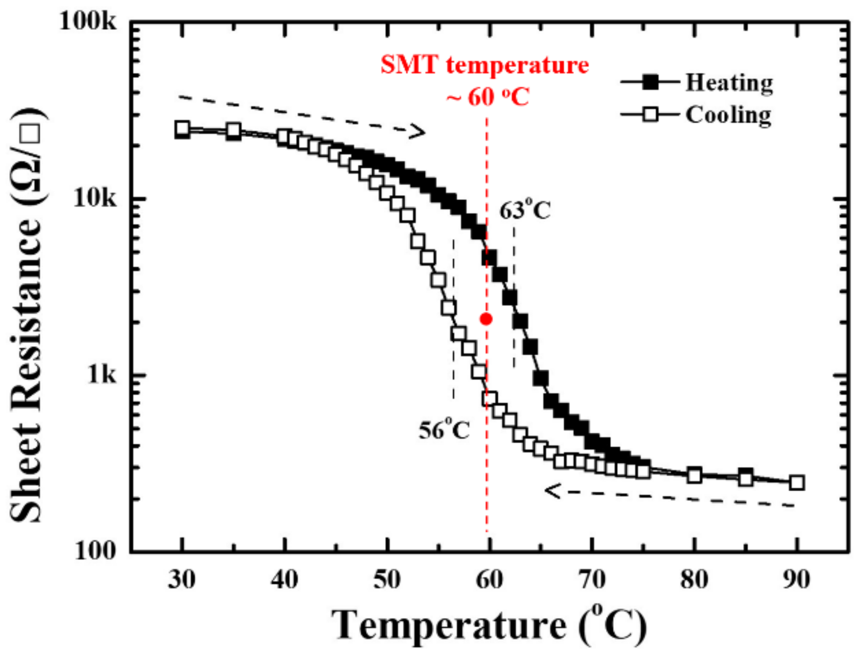
The temperature-dependent sheet-resistance (SR) variation of VO2 film is shown in Figure 6, displaying a thermal hysteresis variation. Besides, the SR variation has approached two orders of magnitude across the semiconductor-to-metal transition (SMT) of the VO2 film (SR changed from 2.2 × 10⁴ to 2.7 × 10² Ω/□ for the temperature raised from 40 to 80 °C) so that the value of the resistance ratio agrees with the typical VO2 film thickness less than 50 nm (typically, the resistance ratios of most VO2 films across the SMT are in the range of 102–103 for thickness <50 nm) [29]. Furthermore, a sharp drop of SR can be clearly observed in the heating cycle, determining a phase transition temperature of about 63 °C, and a sharp rise of SR in the cooling cycle with a phase transition temperature of about 56 °C can be also seen in Figure 6. Therefore, the SMT temperature estimated from the middle of thermal hysteresis SR variation is about 60.0 °C.
There are several parameters that may affect the temperature-dependent electrical properties of VO2, such as changes in impurity content, stoichiometry, strain, oxygen vacancies, and the presence of grain boundaries [8,9,10,11,12]. In this work, the SMT temperature of VO2 film evaluated from the temperature-dependent Raman spectra and sheet-resistance variation is about 61 ± 1 °C, slightly different from the well-known 340K (~67 °C), which can be reasonably attributed to the influence of grain boundary density because the VO2 film has a polycrystalline structure with considerable grain boundaries.
4. Conclusions
In conclusion, the VCl4 is successfully employed as a new ALD precursor to grow a VO2 film on the Si (100) substrate. Besides, without any postannealing process required, the as-deposited VO2 film is directly crystallized and provides a significant SMT property. Moreover, it can be reasonably imagined that the VCl4 can be used not only to grow crystalline VO2 films, but also to grow other different vanadium oxides (VOx, x ≠ 2) by controlling the ALD-process parameters (such as process temperature, VCl4/H2O ratio, and so forth). It is just like this that the VCl4 had been used as a precursor for atmospheric pressure CVD to grow different vanadium oxides (VO2 and V2O5) by controlling process parameters of temperature and VCl4/H2O ratio [30,31,32]. We anticipate this work to be a starting point for using VCl4 as a precursor to grow various directly crystallized vanadium oxides by ALD without any postannealing process.
Supplementary Materials
The following are available online at https://www.mdpi.com/2079-6412/8/12/431/s1, Part 1: A brief report provided by Bruker Corporation for explaining “Why Si (113) peak appears in GIXRD profile?” Part 2: Full temperature-dependent Raman spectra of the VO2 films. Figure S1: Raman spectra of the VO2 film measured at indicant temperature for heating cycle (temperature from 30 to 80 °C), Figure S2: Raman spectra of the VO2 film measured at indicant temperature for cooling cycle (temperature from 78 to 35 °C).
Funding
This research was funded by the Ministry of Science and Technology of Taiwan (Nos.: MOST 105-2221-E-153-001 and MOST 106-2221-E-153-004).
Acknowledgment
The authors would like to thank Dr. Ya-Ching Yang (Bruker Corporation) for discussing and providing a brief report to explain “Why Si (113) peak appears in GIXRD profile?”, Ms. Hui-Jung Shih (Instrument Center, NCKU) for HR-SEM analysis, Ms. Mei-Lan Liang and Ms. Shih-Wen Tseng (Center for Micro/Nano Science and Technology, NCKU) for FIB and TEM analyses, and Ms. Swee-Lan Cheah (Instrument Center, NTHU) for HR-XPS analysis.
Conflicts of Interest
The authors declare no conflict of interest.
References
- Morin, F.J. Oxides which show a metal-to-insulator transition at the Neel temperature. Phys. Rev. Lett. 1959, 3, 34–36. [Google Scholar] [CrossRef]
- Barker, A.S.; Verleur, H.W.; Guggenheim, H.J. Infrared optical properties of vanadium dioxide above and below the transition temperature. Phys. Rev. Lett. 1966, 17, 1286–1289. [Google Scholar] [CrossRef]
- Park, J.H.; Coy, J.M.; Kasirga, T.S.; Huang, C.; Fei, Z.; Hunter, S.; Cobdem, D.H. Measurement of a solid-state triple point at the metal-insulator transition in VO2. Nature 2013, 500, 431–434. [Google Scholar] [CrossRef] [PubMed]
- O’Callahan, B.T.; Jones, A.C.; Park, J.H.; Cobden, D.H.; Atkin, J.M.; Raschke, M.B. Inhomogeneity of the ultrafast insulator-to-metal transition dynamics of VO2. Nat. Commun. 2015, 6, 6849. [Google Scholar] [CrossRef] [PubMed]
- Cueff, S.; Li, D.; Zhou, Y.; Wong, F.J.; Kurvits, J.A.; Ramanathan, S.; Zia, R. Dynamic control of light emission faster than the lifetime limit using VO2 phase-change. Nat. Commun. 2015, 6, 8636. [Google Scholar] [CrossRef] [PubMed]
- Yang, Z.; Ko, C.; Ramanathan, S. Oxide electronics utilizing ultrafast metal-insulator transitions. Annu. Rev. Mater. Res. 2011, 41, 337–367. [Google Scholar] [CrossRef]
- Nakano, M.; Shibuya, K.; Okuyama, D.; Hatano, T.; Ono, S.; Kawasaki, M.; Iwasa, Y.; Tokura, Y. Collective bulk carrier delocalization driven by electrostatic surface charge accumulation. Nature 2012, 487, 459–462. [Google Scholar] [CrossRef] [PubMed]
- Wang, N.; Liu, S.; Zeng, X.T.; Magdassi, S.; Long, Y. Mg/W-codoped vanadium dioxide thin films with enhanced visible transmittance and low phase transition temperature. J. Mater. Chem. C 2015, 3, 6771–6777. [Google Scholar] [CrossRef]
- Zhang, S.; Kim, I.S.; Lauhon, L.J. Stoichiometry engineering of monoclinic to rutile phase transition in suspended single crystalline vanadium dioxide nanobeams. Nano Lett. 2011, 11, 1443–1447. [Google Scholar] [CrossRef] [PubMed]
- Petraru, A.; Soni, R.; Kohlstedt, H. Voltage controlled biaxial strain in VO2 films grown on 0.72Pb(Mg1/3Nb2/3)-0.28PbTiO3 crystals and its effect on the transition temperature. Appl. Phys. Lett. 2014, 105, 092902. [Google Scholar] [CrossRef]
- Jian, J.; Chen, A.; Zhang, W.; Wang, H. Sharp semiconductor-to-metal transition of VO2 thin films on glass substrates. J. Appl. Phys. 2013, 114, 244301. [Google Scholar] [CrossRef]
- Jeong, J.; Aetukuri, N.; Graf, T.; Schladt, T.D.; Samant, M.G.; Parkin, S.S.P. Suppression of metal-insulator transition in VO2 by electric field-induced oxygen vacancy formation. Science 2013, 339, 1402–1405. [Google Scholar] [CrossRef] [PubMed]
- Aetukuri, N.B.; Gary, A.X.; Drouard, M.; Cossale, M.; Gao, L.; Reid, A.H.; Kukreja, R.; Ohldag, H.; Jenkins, C.A.; Arenholz, E.; et al. Control of the metal–insulator transition in vanadium dioxide by modifying orbital occupancy. Nat. Phys. 2013, 9, 661–666. [Google Scholar] [CrossRef]
- Wu, J.M.; Liou, L.B. Room temperature photo-induced phase transitions of VO2 nanodevices. J. Mater. Chem. 2011, 21, 5499–5504. [Google Scholar] [CrossRef]
- Xu, F.; Cao, X.; Luo, H.; Jin, P. Recent advances in VO2-based thermochromic composites for smart windows. J. Mater. Chem. C 2018, 6, 1903–1919. [Google Scholar] [CrossRef]
- Shukla, N.; Parihar, A.; Freeman, E.; Paik, H.; Stone, G.; Narayanan, V.; Wen, H.; Cai, Z.; Gopalan, V.; Engel-Herbert, R.; et al. Synchronized charge oscillations in correlated electron systems. Sci. Rep. 2014, 4, 4964. [Google Scholar] [CrossRef]
- Ruzmetov, D.; Gopalakrishnan, G.; Ko, C.; Narayanamurti, V.; Ramanathan, S. Three-terminal field effect devices utilizing thin film vanadium oxide as the channel layer. J. Appl. Phys. 2010, 107, 114516. [Google Scholar] [CrossRef] [Green Version]
- Yajima, T.; Nishimura, T.; Toriumi, A. Positive-bias gate-controlled metal–insulator transition in ultrathin VO2 channels with TiO2 gate dielectrics. Nat. Commun. 2015, 6, 10104. [Google Scholar] [CrossRef] [PubMed]
- Briggs, R.M.; Pryce, I.M.; Atwater, H.A. Compact silicon photonic waveguide modulator based on the vanadium dioxide metal-insulator phase transition. Opt. Express 2010, 18, 11192–11201. [Google Scholar] [CrossRef] [PubMed]
- Gu, Q.; Falk, A.; Wu, J.Q.; Ouyang, L.; Park, H. Current-driven phase oscillation and domain-wall propagation in WxV1-xO2 nanobeams. Nano Lett. 2007, 7, 363–366. [Google Scholar] [CrossRef] [PubMed]
- Dicken, M.J.; Aydin, K.; Pryce, I.M.; Sweatlock, L.A.; Boyd, E.M.; Walavalkar, S.; Ma, J.; Atwater, H.A. Frequency tunable near-infrared metamaterials based on VO2 phase transition. Opt. Express 2009, 17, 18330–18339. [Google Scholar] [CrossRef] [PubMed]
- Driscoll, T.; Kim, H.T.; Chae, B.G.; Di Ventra, M.; Basov, D.N. Phase-transition driven memristive system. Appl. Phys. Lett. 2009, 95, 043503. [Google Scholar] [CrossRef] [Green Version]
- Kim, B.J.; Lee, Y.W.; Chae, B.G.; Yun, S.J.; Oh, S.Y.; Kim, H.T. Temperature dependence of the first-order metal-insulator transition in VO2 and programmable critical temperature sensor. Appl. Phys. Lett. 2007, 90, 023515. [Google Scholar] [CrossRef]
- Strelcov, E.; Lilach, Y.; Kolmakov, A. Gas sensor based on metal-insulator transition in VO2 nanowire thermistor. Nano Lett. 2009, 9, 2322–2326. [Google Scholar] [CrossRef] [PubMed]
- Heckman, E.M.; Gonzalez, L.P.; Guha, S.; Barnes, J.O.; Carpenter, A. Electrical and optical switching properties of ion implanted VO2 thin films. Thin Solid Films 2009, 518, 265–268. [Google Scholar] [CrossRef]
- Ureña-Begara, F.; Crunteanu, A.; Raskin, J.P. Raman and XPS characterization of vanadium oxide thin films with temperature. Appl. Surf. Sci. 2017, 403, 717–727. [Google Scholar] [CrossRef] [Green Version]
- Chiu, T.W.; Tonooka, K.; Kikuchi, N. Growth of b-axis oriented VO2 thin films on glass substrates using ZnO buffer layer. Appl. Surf. Sci. 2010, 256, 6834–6837. [Google Scholar] [CrossRef]
- Zhang, P.; Jiang, K.; Deng, Q.; You, Q.; Zhang, J.; Wu, J.; Hu, Z.; Chu, J. Manipulations from oxygen partial pressure on the higher energy electronic transition and dielectric function of VO2 films during a metal-insulator transition process. J. Mater. Chem. C 2015, 3, 5033–5040. [Google Scholar] [CrossRef]
- Zhang, H.T.; Zhang, L.; Mukherjee, D.; Zheng, Y.X.; Haislmaier, R.C.; Alem, N.; Engel-Herbert, R. Wafer-scale growth of VO2 thin films using a combinatorial approach. Nat. Commun. 2015, 6, 8475. [Google Scholar] [CrossRef] [PubMed]
- Vernardou, D.; Pemble, M.E.; Sheel, D.W. The growth of thermochromic VO2 films on glass by atmospheric-pressure CVD: A comparative study of precursors, CVD methodology, and substrates. Chem. Vap. Depos. 2006, 12, 263–274. [Google Scholar] [CrossRef]
- Vernardou, D.; Paterakis, P.; Drosos, H.; Spanakis, E.; Povey, I.M.; Pemble, M.E.; Koudoumas, E.; Katsarakis, N. A study of the electrochemical performance of vanadium oxide thin films grown by atmospheric pressure chemical vapour deposition. Sol. Energy Mater. Sol. Cells 2011, 95, 2842–2847. [Google Scholar] [CrossRef]
- Vernardou, D. Using an atmospheric pressure chemical vapor deposition process for the development of V2O5 as an electrochromic material. Coatings 2017, 7, 24. [Google Scholar] [CrossRef]
- Makarevich, A.M.; Sadykov, I.I.; Sharovarov, D.I.; Amelichev, V.A.; Adamenkov, A.A.; Tsymbarenko, D.M.; Plokhih, A.V.; Esaulkov, M.N.; Solyankin, P.M.; Kaul, A.R. Chemical synthesis of high quality epitaxial vanadium dioxide films with sharp electrical and optical switch properties. J. Mater. Chem. C 2015, 3, 9197–9205. [Google Scholar] [CrossRef]
- Blackburn, B.; Powell, M.J.; Knapp, C.E.; Bear, J.C.; Carmalt, C.J.; Parkin, I.P. [{VOCl2(CH2(COOEt)2)}4] as a molecular precursor for thermochromic monoclinic VO2 thin films and nanoparticles. J. Mater. Chem. C 2016, 4, 10453–10463. [Google Scholar] [CrossRef]
- Rampelberg, G.; Schaekers, M.; Martens, K.; Xie, Q.; Deduytsche, D.; De Schutter, B.; Blasco, N.; Kittl, J.; Detavernier, C. Semiconductor-metal transition in thin VO2 films grown by ozone based atomic layer deposition. Appl. Phys. Lett. 2011, 98, 162902. [Google Scholar] [CrossRef]
- Premkumar, P.A.; Toeller, M.; Radu, I.P.; Adelmann, C.; Schaekers, M.; Meersschaut, J.; Conard, T.; Elshocht, S.V. Process study and characterization of VO2 thin films synthesized by ALD using TEMAV and O3 precursors. ECS J. Solid State Sci. Technol. 2012, 1, P169–P174. [Google Scholar] [CrossRef]
- Tangirala, M.; Zhang, K.; Nminibapiel, D.; Pallem, V.; Dussarrat, C.; Cao, W.; Adam, T.N.; Johnson, C.S.; Elsayed-Ali, H.E.; Baumgart, H. Physical analysis of VO2 films grown by atomic layer deposition and RF magnetron sputtering. ECS J. Solid State Sci. Technol. 2014, 3, N89–N94. [Google Scholar] [CrossRef]
- Cerbu, F.; Chou, H.S.; Radu, I.P.; Martens, K.; Peter, A.P.; Afanas’ev, V.V.; Stesmans, A. Band alignment and effective work function of atomic-layer deposited VO2 and V2O5 films on SiO2 and Al2O3. Phys. Status Solidi C 2015, 12, 238–241. [Google Scholar] [CrossRef]
- Zhang, K.; Tangirala, M.; Nminibapiel, D.; Cao, W.; Pallem, V.; Dussarrat, C.; Baumgart, H. Synthesis of VO2 thin films by atomic layer deposition with TEMAV as precursor. ECS Trans. 2013, 50, 175–182. [Google Scholar] [CrossRef]
- Blanquart, T.; Niinistö, J.; Gavagnin, M.; Longo, V.; Heikkilä, M.; Puukilainen, E.; Pallem, V.R.; Dussarrat, C.; Ritala, M.; Leskelä, M. Atomic layer deposition and characterization of vanadium oxide thin films. RSC Adv. 2013, 3, 1179–1185. [Google Scholar] [CrossRef]
- Kozen, A.C.; Joress, H.; Currie, M.; Anderson, V.R.; Eddy, C.R., Jr.; Wheeler, V.D. Structural characterization of atomic layer deposited vanadium dioxide. J. Phys. Chem. C 2017, 121, 19341–19347. [Google Scholar] [CrossRef]
- Park, H.H.; Larrabee, T.J.; Ruppalt, L.B.; Culbertson, J.C.; Prokes, S.M. Tunable electrical properties of vanadium oxide by hydrogen-plasma-treated atomic layer deposition. ACS Omega 2017, 2, 1259–1264. [Google Scholar] [CrossRef]
- Musschoot, J.; Deduytsche, D.; Poelman, H.; Haemers, J.; Van Meirhaeghe, R.L.; Van den Berghe, S.; Detavernier, C. Comparison of thermal and plasma-enhanced ALD/CVD of vanadium pentoxide. J. Electrochem. Soc. 2009, 156, P122–P126. [Google Scholar] [CrossRef]
- Boukhalfa, S.; Evanoff, K.; Yushin, G. Atomic layer deposition of vanadium oxide on carbon nanotubes for high-power supercapacitor electrodes. Energy Environ. Sci. 2012, 5, 6872–6879. [Google Scholar] [CrossRef]
- Singh, T.; Wang, S.; Aslam, N.; Zhang, H.; Hoffmann-Eifert, S.; Mathur, S. Atomic layer deposition of transparent VOx thin films for resistive switching applications. Chem. Vap. Depos. 2014, 20, 291–297. [Google Scholar] [CrossRef]
- Daubert, J.S.; Lewis, N.P.; Gotsch, H.N.; Mundy, J.Z.; Monroe, D.N.; Dickey, E.C.; Losego, M.D.; Parsons, G.N. Effect of meso- and micro-porosity in carbon electrodes on atomic layer deposition of pseudocapacitive V2O5 for high performance supercapacitors. Chem. Mater. 2015, 27, 6524–6534. [Google Scholar] [CrossRef]
- Baddour-Hadjean, R.; Golabkan, V.; Pereira-Ramos, J.P.; Mantoux, A.; Lincot, D. A Raman study of the lithium insertion process in vanadium pentoxide thin films deposited by atomic layer deposition. J. Raman Spectrosc. 2002, 33, 631–638. [Google Scholar] [CrossRef]
- Badot, J.C.; Mantoux, A.; Baffier, N.; Dubrunfaut, O.; Lincot, D. Electrical properties of V2O5 thin films obtained by atomic layer deposition (ALD). J. Mater. Chem. 2004, 14, 3411–3415. [Google Scholar] [CrossRef]
- Chen, X.; Pomerantseva, E.; Banerjee, P.; Gregorczyk, K.; Ghodssi, R.; Rubloff, G. Ozone-based atomic layer deposition of crystalline V2O5 films for high performance electrochemical energy storage. Chem. Mater. 2012, 24, 1255–1261. [Google Scholar] [CrossRef]
- Badot, J.C.; Ribes, S.; Yousfi, E.B.; Vivier, V.; Pereira-Ramos, J.P.; Baffier, N.; Lincot, D. Atomic layer epitaxy of vanadium oxide thin films and electrochemical behavior in presence of lithium ions. Electrochem. Solid-State Lett. 2000, 3, 485–488. [Google Scholar] [CrossRef]
- Kim, H.; Maeng, W.J. Applications of atomic layer deposition to nanofabrication and emerging nanodevices. Thin Solid Films 2009, 517, 2563–2580. [Google Scholar] [CrossRef]
- George, S.M. Atomic layer deposition: An overview. Chem. Rev. 2010, 110, 111–131. [Google Scholar] [CrossRef] [PubMed]
- Gelde, L.; Cuevas, A.L.; Martínez de Yuso, M.D.V.; Benavente, J.; Vega, V.; Gonzalez, A.S.; Prida, V.M.; Hernando, B. Influence of TiO2-coating layer on nanoporous alumina membranes by ALD technique. Coatings 2018, 8, 60. [Google Scholar] [CrossRef]
- Cheng, H.E.; Lee, W.J. Properties of TiN films grown by atomic-layer chemical vapor deposition with a modified gaseous-pulse sequence. Mater. Chem. Phys. 2006, 97, 315–320. [Google Scholar] [CrossRef]
- Lee, W.J.; Hon, M.H. Space-limited crystal growth mechanism of TiO2 films by atomic layer deposition. J. Phys. Chem. C 2010, 114, 6917–6921. [Google Scholar] [CrossRef]
- Wu, C.; Zhang, X.; Dai, J.; Yang, J.; Wu, Z.; Wei, S.; Xie, Y. Direct hydrothermal synthesis of monoclinic VO2(M) single-domain nanorods on large scale displaying magnetocaloric effect. J. Mater. Chem. 2011, 21, 4509–4517. [Google Scholar] [CrossRef]
- Silversmit, G.; Depla, D.; Poelman, H.; Martin, G.B.; De Gryse, R. Determination of the V2p XPS binding energies for different vanadium oxidation states (V5+ to V0+). J. Electron. Spectrosc. Relat. Phenom. 2004, 135, 167–175. [Google Scholar] [CrossRef]
- Hryha, E.; Rutqvist, E.; Nyborg, L. Stoichiometric vanadium oxides studied by XPS. Surf. Interface Anal. 2012, 44, 1022–1025. [Google Scholar] [CrossRef]
- Yuan, X.; Zhang, W.; Zhang, P. Hole-lattice coupling and photoinduced insulator-metal transition in VO2. Phys. Rev. B 2013, 88, 035119. [Google Scholar] [CrossRef]
- Zaghrioui, M.; Sakai, J.; Azhan, N.H.; Su, K.; Okimura, K. Polarized Raman scattering of large crystalline domains in VO2 films on sapphire. Vib. Spectrosc. 2015, 80, 79–85. [Google Scholar] [CrossRef]
- Shibuya, K.; Sawa, A. Polarized Raman scattering of epitaxial vanadium dioxide films with low-temperature monoclinic phase. J. Appl. Phys. 2017, 122, 015307. [Google Scholar] [CrossRef]
Figure 1.
XRD patterns of VO2 film measured at (a) 30 °C and (b) 90 °C. (c) A comparison of (a) and (b).
Figure 1.
XRD patterns of VO2 film measured at (a) 30 °C and (b) 90 °C. (c) A comparison of (a) and (b).
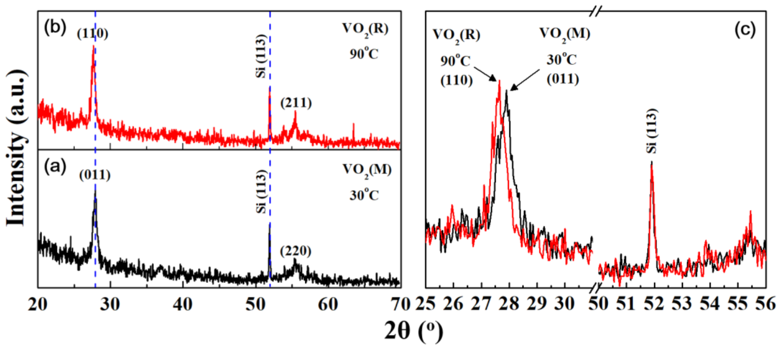
Figure 2.
Microstructure analyses of VO2 film. (a) An SEM top-view image. TEM cross-sectional (b) bright-field and (c) dark-field images. (d) A high-resolution TEM (HR-TEM) image of the VO2/SiOx/Si interface. (e) The selected-area electron-beam diffraction (SA-EBD) pattern obtained by focusing the electron beam on an individual VO2 grain.

Figure 3.
(a) V2p, (b) O1s, and (c) Cl2p XPS spectra for original (before etching) and after argon-ion etching surface of VO2 film.
Figure 3.
(a) V2p, (b) O1s, and (c) Cl2p XPS spectra for original (before etching) and after argon-ion etching surface of VO2 film.
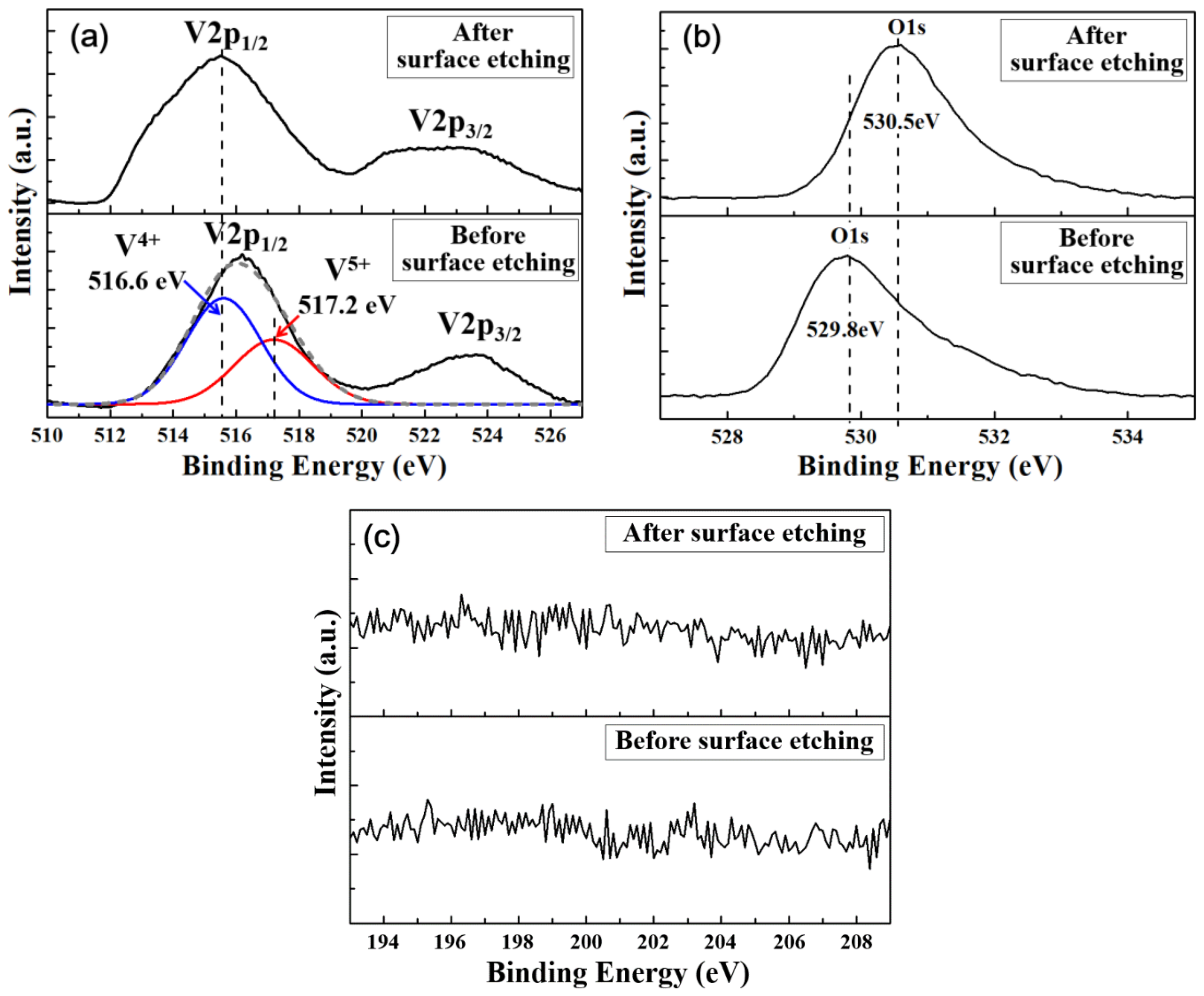
Figure 4.
Temperature-dependent Raman spectra of the VO2 film: (a) heating cycle, (b) cooling cycle, and relative Raman intensity of the Ag phonon mode at (c) 194, (d) 224, and (e) 616 cm−1.
Figure 4.
Temperature-dependent Raman spectra of the VO2 film: (a) heating cycle, (b) cooling cycle, and relative Raman intensity of the Ag phonon mode at (c) 194, (d) 224, and (e) 616 cm−1.
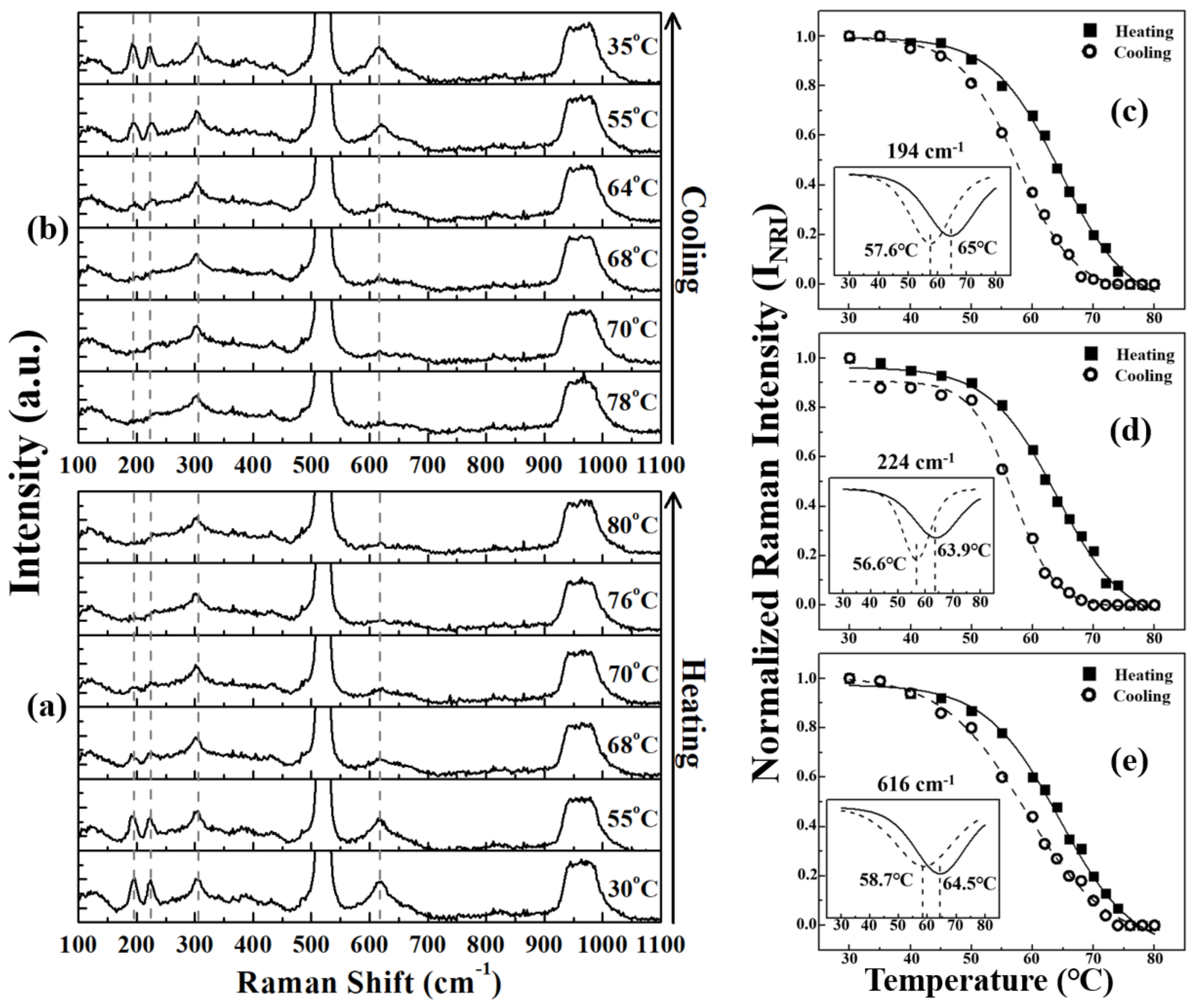
Figure 5.
Raman spectrum of the silicon substrate.
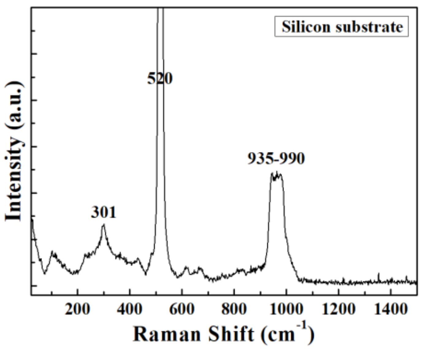
Figure 6.
Temperature-dependent sheet-resistance variation of the VO2 film.

Table 1.
Chemical composition of VO2 thin film analyzed by XPS.
| Elemental Content | Before Surface Etching | After Surface Etching |
|---|---|---|
| V (at.%) | 25.7 | 33.1 |
| O (at.%) | 74.3 | 66.9 |
| Cl (at.%) | <0.1 | <0.1 |
© 2018 by the authors. Licensee MDPI, Basel, Switzerland. This article is an open access article distributed under the terms and conditions of the Creative Commons Attribution (CC BY) license (http://creativecommons.org/licenses/by/4.0/).
Share and Cite
MDPI and ACS Style
Lee, W.-J.; Chang, Y.-H. Growth without Postannealing of Monoclinic VO2 Thin Film by Atomic Layer Deposition Using VCl4 as Precursor. Coatings 2018, 8, 431. https://doi.org/10.3390/coatings8120431
AMA Style
Lee W-J, Chang Y-H. Growth without Postannealing of Monoclinic VO2 Thin Film by Atomic Layer Deposition Using VCl4 as Precursor. Coatings. 2018; 8(12):431. https://doi.org/10.3390/coatings8120431
Chicago/Turabian StyleLee, Wen-Jen, and Yong-Han Chang. 2018. "Growth without Postannealing of Monoclinic VO2 Thin Film by Atomic Layer Deposition Using VCl4 as Precursor" Coatings 8, no. 12: 431. https://doi.org/10.3390/coatings8120431
Note that from the first issue of 2016, this journal uses article numbers instead of page numbers. See further details here.