Extinction Properties of Obliquely Deposited TiN Nanorod Arrays


Department of Electro-Optical Engineering, National Taipei University of Technology, Taipei 106, Taiwan
*
Author to whom correspondence should be addressed.
Coatings 2018, 8(12), 465; https://doi.org/10.3390/coatings8120465
Submission received: 3 November 2018
/
Revised: 11 December 2018
/
Accepted: 13 December 2018
/
Published: 14 December 2018
(This article belongs to the Special Issue Design, Manufacturing and Measurement of Optical Film Coatings)
Abstract
:Plasmonic titanium nitride (TiN) nanorod arrays (NRA) were fabricated by glancing angle deposition in a DC magnetron reactive sputtering system. The morphology of the TiN NRA was varied by collimating the vapor flux. The transmittance, reflectance, and extinctance of slanted TiN nanorods with different lengths as functions of wavelength and angle of incidence were measured and analyzed. The extinction peaks in the spectra reveal the transverse and longitudinal plasmonic modes of TiN NRA upon excitation by s-polarized and p-polarized light, respectively. The near-field simulation was performed to elucidate localized field enhancements that correspond to high extinction. The extension of the high extinction band with an increasing length of the nanorods results in broadband and wide-angle light extinction for a TiN NRA with a thickness greater than 426 nm.
1. Introduction
In recent years, nanostructures made of plasmonic materials have held a very important position in the field of science and technology. The traditional metals preferred for plasmonic materials have high resistance loss. Even metals with the highest conductivity (e.g., silver, gold) exhibit excessive loss at optical frequencies to limit the development of optical components. The plasmonic material has been implemented in many fields such as light control, sensors, nanoscale waveguides, and high-density data storage [1,2,3]. However, because of limitations in material properties such as ductility, incompatibility in the manufacturing process, and chemical instability, most of these materials remain in the experimental stage. Recently, transition metal nitrides (TMN) such as titanium nitride (TiN) and zirconium nitride (ZrN) exhibit unique material properties, meaning they have potential as plasmonic materials for various applications [4,5,6]. In addition to the plasmonic properties in the visible and infrared regions, these materials are mechanically and chemically stable and can operate under harsh environmental conditions. With a high melting point and chemical stability at temperatures above 2900 °C, TMNs exhibit a mechanical refractory property and have the same optical property as noble metals [7]. Owing to their high carrier concentration, which supports negative real permittivity and relatively high carrier mobility, TMNs are candidates to replace noble metals in plasmonic applications [8]. Therefore, TMN has strong potential as a heat-resistant, lightweight, and efficient optical component, such as in aerospace engineering. In TMN, TiN is the first choice in several areas, including in wear resistant coatings, biomedical areas, and microelectronics [9]. Combining the benefits of the above TiN, the nanostructure of TiN begins to attract attention. A typical associated application of TiN is in thermophotovoltaic devices, in which TiN is used as an intermediate component to absorb solar irradiation, and heated TiN radiates thermal radiation at a high temperature in a narrow spectrum for efficient absorption by the photovoltaic cell [10]. Therefore, TiN is formed as a variously shaped nanoparticle with plasmonic effects. TiN square rings of 250 nm × 250 nm are regularly distributed on SiO2 films that are coated on silicon to provide high absorptance over 85% over wavelengths from 400 to 800 nm [11]. Such a nanopatterned structure can be heated for four hours at 800 °C. TiN nanoparticles can replace gold particles in thermal therapy, owing to their biocompatibility and wide plasmon resonance band, which is wide enough to support the biological transparency window [12,13]. TiN nanorod arrays (NRA) were fabricated for surface-enhanced Raman scattering (SERS) [14,15,16]. The SERS spectra of rhodamine 6G that were adsorbed on fresh TiN NRA substrate and the same substrate that had been stored for 40 days were obtained. After 40 days, the measured intensity of SERS was reduced by 12% relative to that measured on fresh substrate [17]. The high stability of the Raman spectrum revealed a potential application of TiN NRAs in SERS. As a traditional hard coating, TiN films have been prepared in physical vapor deposition systems using low-voltage electron beam evaporation, high-voltage electron beam evaporation, random arc evaporation steer arc evaporation, and magnetron sputtering [18,19,20,21]. Because TMNs have been the alternative plasmonic material with refractory property, the optical property associated with localized plasmonic resonance among nanostructure is desired to be observed. Glancing angle deposition (GLAD) is a simple method to sculpture various nanostructures such as slanted rod array, spiral, and zigzag structures by manipulating the orientation of substrate during deposition [22,23]. The anisotropic optical property of a nanorod array has been applied to fabricate novel optical devices including polarization beam splitter [24], achromatic waveplate [25], and high-efficiency light absorber [26]. However, the research of nanostructures with TMNs made by GLAD has been getting started in recent years. In a recent work, GLAD was used to grow a tilted TiO2 nanorod array (NRA) by electron beam evaporation, and the TiO2 NRA was then transformed into TiN NRA via nitridation with annealing [27]. In this investigation, glancing angle deposited TiN NRAs were grown in a magnetic sputtering system. Some previous works [28,29,30] used the same method to deposit TiN NRAs by tuning the deposition angle. The morphology of TiN NRA is slightly dependent on the deposition angle. In this work, NRAs were deposited with and without high collimated flux to cause high variation of tilt angle of rods. On the other hand, different thicknesses (rod lengths) of the rods were fabricated, and the corresponding transmittance, reflectance, and extinctance spectra at different angles of incidence were obtained and analyzed. The localized plasmonic resonance corresponding to high-efficiency light extinction was simulated using finite-difference time-domain (FDTD).
2. Experiments and Results
2.1. Fabrication and Measurement of Uniform TiN Thin Films
Thin films of TiN were deposited on glass substrates by DC reactive magnetron sputtering (PVD Products Inc., Wilmington, NC, USA) using a 99.995% titanium target (Kurt Lesker, Jefferson Hills, PA, USA) in an argon–nitrogen environment. The base pressure in the chamber before deposition was 4 × 10⁻⁶ Torr. The films were deposited at a pressure of 5 × 10⁻⁵ Torr with varying flow ratios of argon to nitrogen (of 30:5, 30:3.5, and 30:1.5). The sputtering power was constant for all depositions at 200 W (DC). The deposition rate was approximately 2.5 nm·min−1.
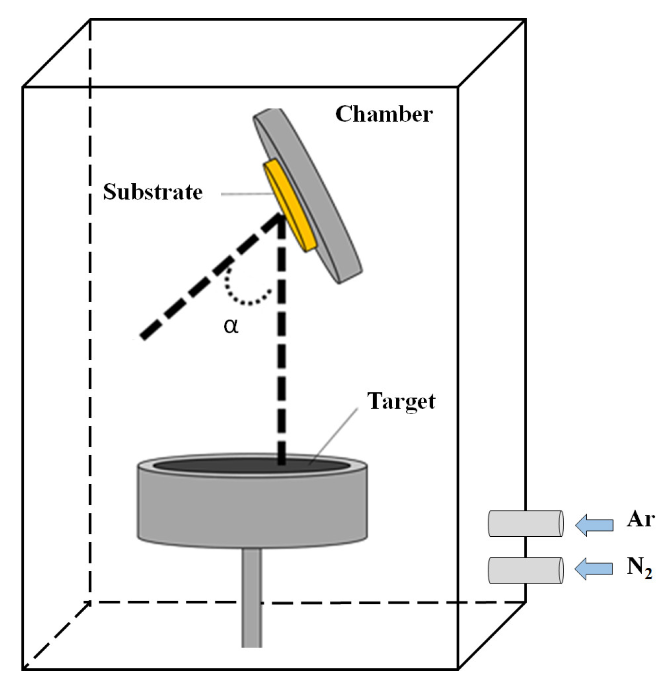
Figure 1 shows the deposition system. A planar magnetron with a target diameter of 75 mm was mounted at the bottom of a chamber. The substrate was mounted on a rotation stage whose center was 150 mm vertically above the target and shifted by 60 mm horizontally from the center of the target. To deposit TiN, a pure Ti target was used with Ar as the sputtering gas and N2 as the reactive gas. To obtain stoichiometric TiN, the argon flow was kept at 30 sccm and the N2 flow rate was varied from RN2 = 1.5 sccm to 5 sccm. The deposition angle α is the angle between the surface normal and vertical. TiN coatings were deposited at an operating pressure that varied with the Ar flow rate.
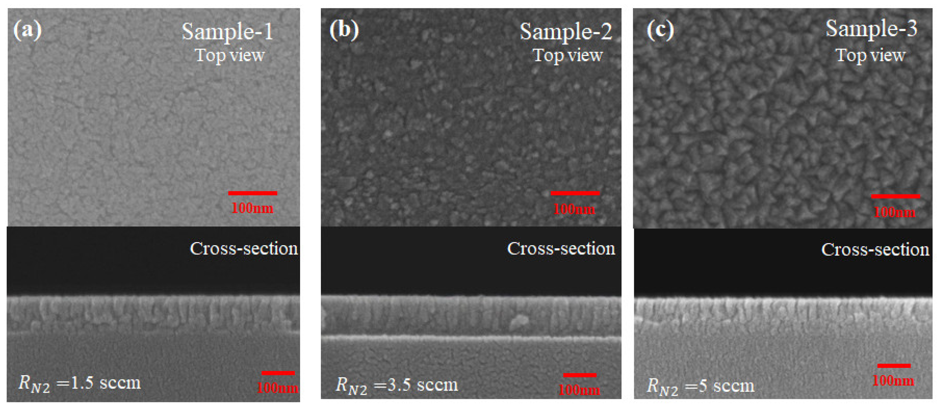
First, three TiN thin films, Sample-1, Sample-2, and Sample-3, were deposited at a deposition angle of α = 0° with RN2 = 1.5 sccm, RN2 = 3.5 sccm, and RN2 = 5 sccm, respectively. The deposited TiN thin films analyzed by X-ray photoelectron spectroscopy (XPS, Thermo VG-Scientific, Waltham, MA, USA) and variable angle spectroscopic ellipsometry (VASE, J. A. Woollam Co., Lincoln, NE, USA). Figure 2 shows the cross-section and top-view scanning electron microscopic (SEM, JEOL, Tokyo, Japan) images of each sample. The thicknesses of the three samples were derived from the morphologies of the TiN thin films: d1 = 109 nm, d2 = 112 nm, and d3 = 113 nm.
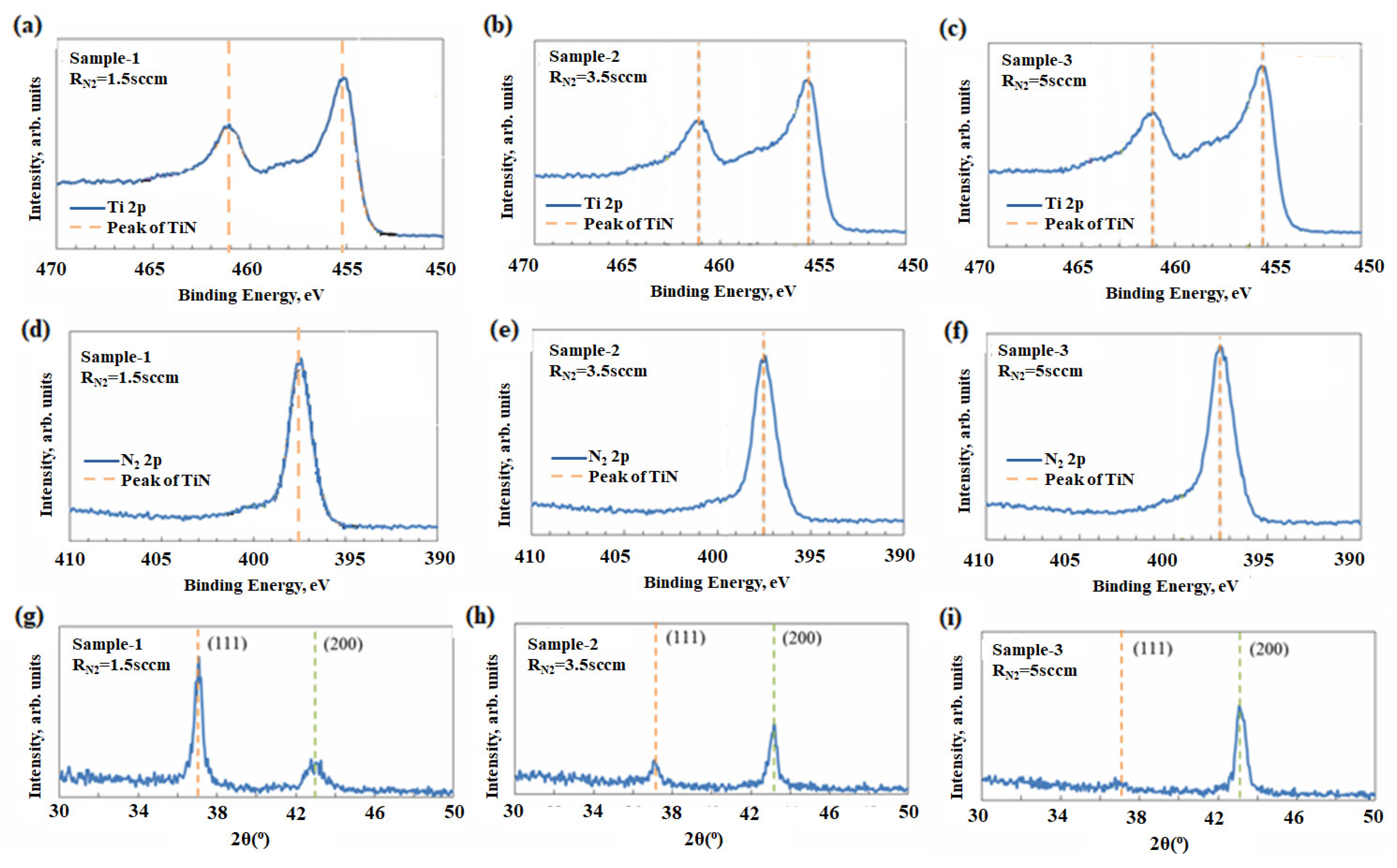
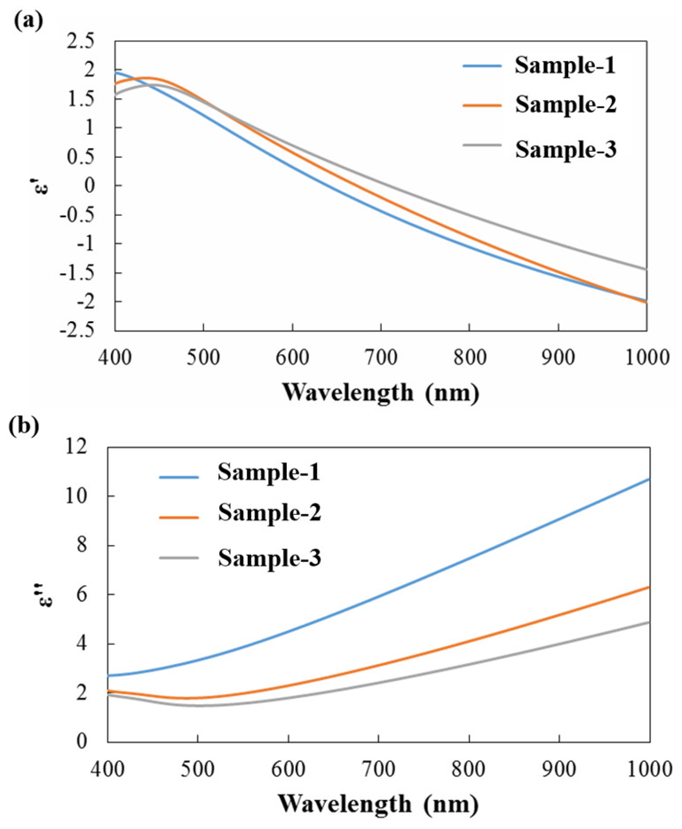
Figure 3a–f shows the Ti 2p and N 1s photoemission core level spectra of the three samples. The peaks in those spectra were at binding energies that corresponded to the characteristics of TiN. Crystallite structures were determined by an X-ray diffraction (XRD, D/MAX2500PC, Rigaku, Tokyo, Japan), as shown in Figure 3g–i. As the nitrogen flow rate was increased, the intensity of crystalline (200) increased and that of crystalline (111) decreased, consistent with previous findings [31]. The optical properties of TiN film were measured using variable angle spectroscopic ellipsometry at incident angles of 45° and 70° for wavelengths from 400 to 1000 nm. The permittivity of TiN was extracted by fitting the spectroscopic parameters of the polarization ellipse with the Drude−Lorentz model [32]. The permittivity ε = ε’ + ε” of each sample was measured as a function of wavelength using an ellipsometer, as presented in Figure 4. The real permittivity as a function of wavelength indicates that the cross wavelength λc increased from 640 to 710 nm as the flow rate of nitrogen increased from 1.5 to 5 sccm. The imaginary permittivity decreased over the wavelengths from 400 to 1000 nm as the flow rate of nitrogen increased from 1.5 to 5 sccm.
2.2. Glancing Angle-Deposited TiN Nanorod Arrays (NRA)
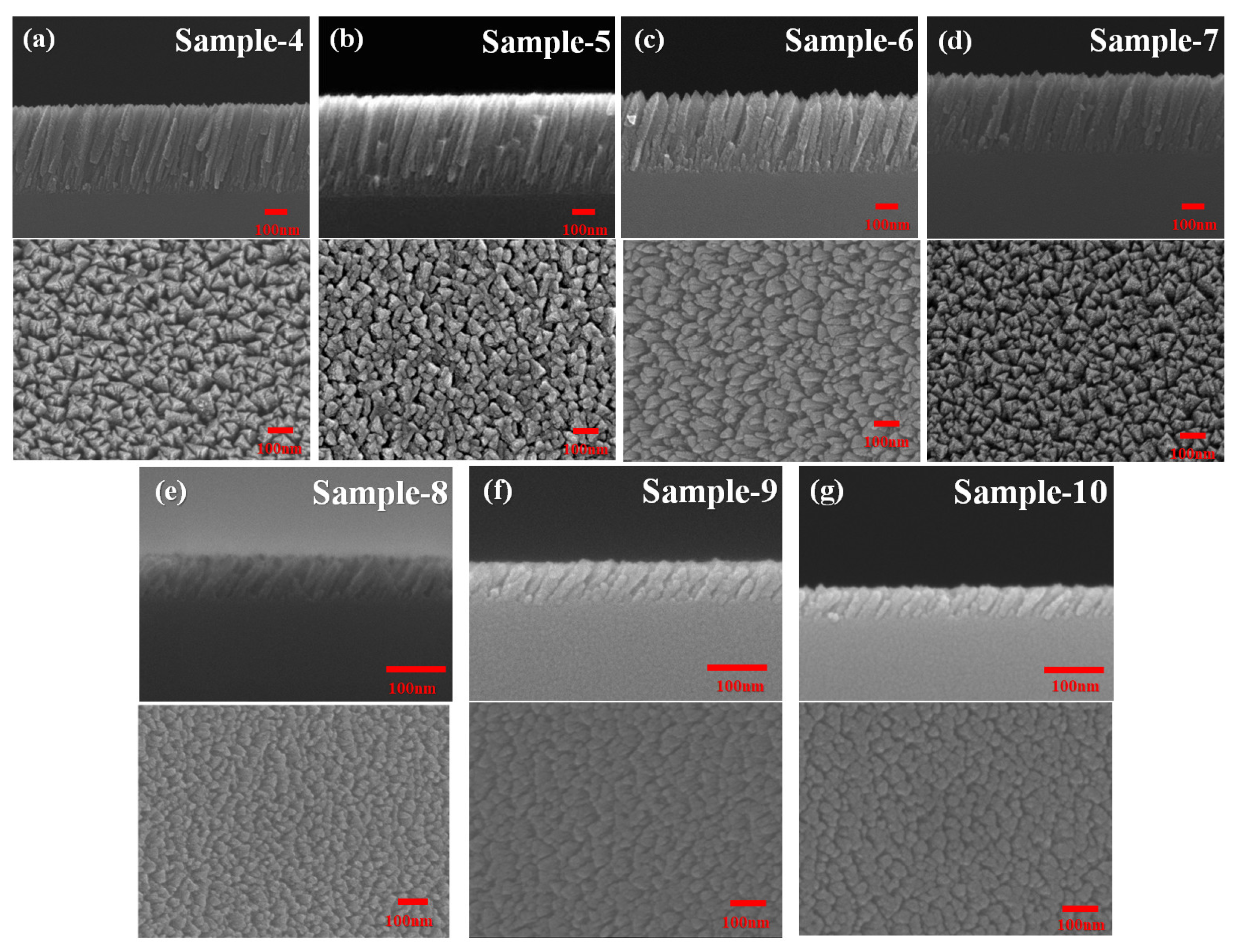
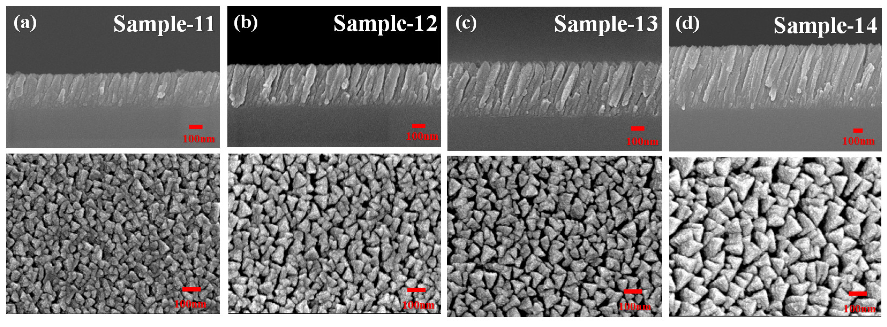
GLAD was used to grow a slanted nanorod array by tilting the substrate with respect to the vertical [33]. The nitrogen flow rate was maintained at 3.5 sccm. Four samples, Sample-4, Sample-5, Sample-6, and Sample-7, were deposited at α of 75°, 80°, 85°, and 88°, respectively. Figure 5 shows top-view and cross-section scanning electron microscopic (SEM) images of TiN NRA. TiN NRAs were coated on the substrate with the size of 1 in2. According to the film thickness between closest and farthest positions from the SEM, the variation of thickness of TiN films were less than 20 nm. Table 1 presents the morphological parameters, including average tilt angle between the slanted rod and the surface normal β, rod width w, length of rod l, spacing between adjacent rods p, porosity, and thicknesses d. The porosity of TiN NRAs was estimated from the SEM by using an image processing program (Image J, 1.48). The average tilt angle of the rods remained at 18.3° ± 0.4°, indicating a weak dependence on deposition angle. The widths of four samples, within the range 44.9 ± 10.6 nm, also did not vary with deposition angle. Although the porosity increased as α increased, β should be changed with α in GLAD. As the target was much larger than the substrate, the incoming flux arrived at the substrate from various directions. The variation of β caused by the shadowing effect [34] has been greatly weakened. Besides, β can also be controlled by limiting the direction of the deposition flux. To limit the distribution of deposition angles, the flux was collimated using a plate above and parallel to the substrate, separated by 10 mm [35]. Sample-8, Sample-9, and Sample-10 were fabricated at deposition angles of 80°, 85°, and 88°. The collimation reduced the rod width to 22.9 ± 4.5 nm and increased the average tilt angle of the rods to 38.3° ± 0.8°. As the deposition angle of incidence increased from 80° to 88°, the tilt angle β increased slightly from 37.4° to 39.1°. By limiting the direction of the deposition flux, the shadowing effect effectively dominated the average tilt angle increased from 18.3° to 39.1°. In addition, obvious rods inclination occurred at α of 80°, 85°, and 88°, according to the results of Sample-4 to Sample-7. The middle angle of α = 85° chosen to grow the samples used in the discussion of the effect of the length of the TiN nanorods on optical property. Figure 6 shows the morphology of Sample-11, Sample-12, Sample-13, and Sample-14 with thicknesses of 267, 329, 426, and 690 nm, respectively. As the thickness increased from 267 to 690 nm, the mean width of the nanorods increased from 57.8 to 93.7 nm. The fan-out phenomenon of the nanorod was caused by surface diffusion of particles as the thickness increased.
2.3. Optical Measurement and Analysis for TiN NRAs
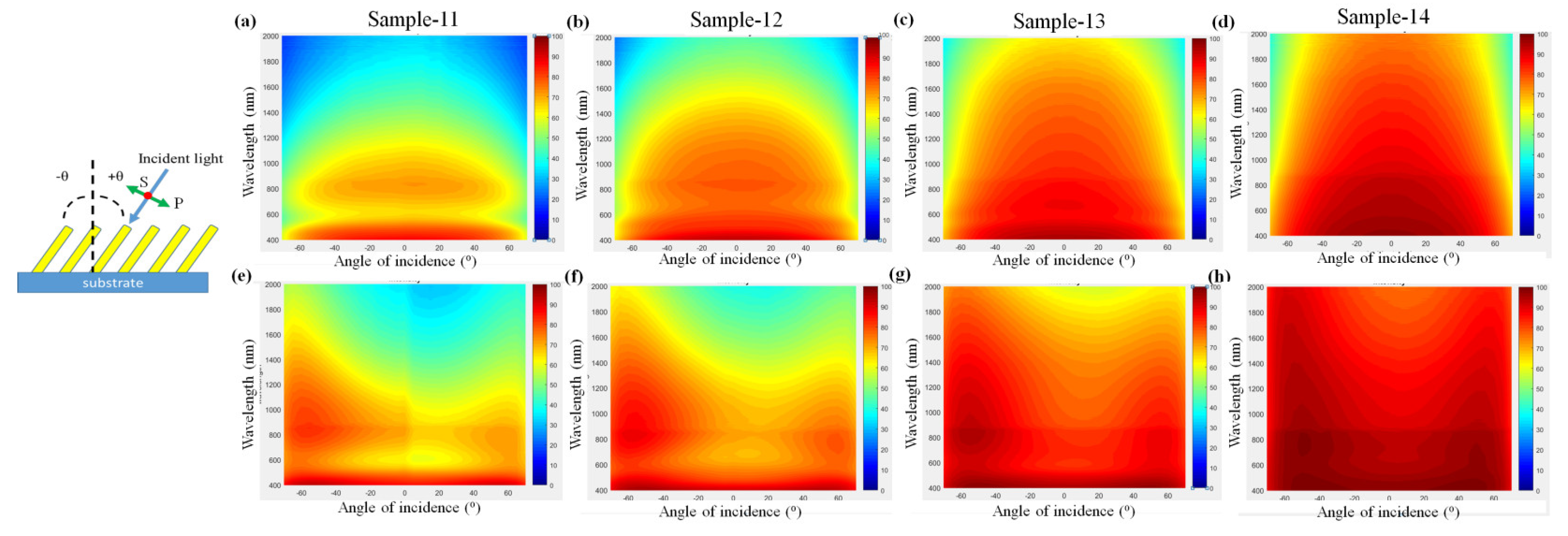
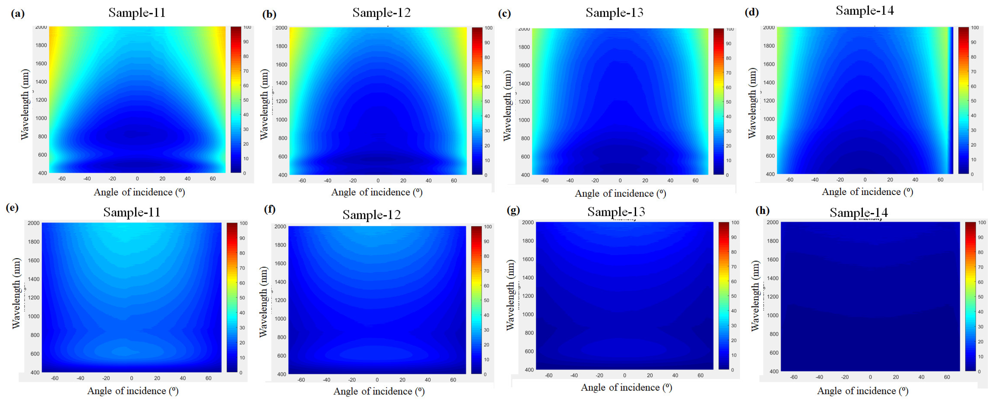
A linear polarized light was used to measure reflectance R and transmittance T of the four samples, as functions of wavelength λ and angle of incidence θ, by Hitachi 4150 spectrophotometer (Tokyo, Japan). TiN NRAs were measured by attaching the samples to an integrating sphere to collect both diffuse and specular light intensities. Figure 7 shows the extinctance E, given by 1–R−T. The plane of incidence was set to be coincident with the plane that contained surface normal and the growth direction of the nanorods. The angle of incidence, θ, was defined as negative or positive according to the illustration shown in the left of Figure 7. As shown in Figure 7a–d, the s-polarized extinctance of each sample has high values over 88% at wavelengths around 400 nm between θ = −60° and θ = 60°. Notably, a extinctance dip occurs around λ = 600 nm at θ between −40° and 40° for the thinnest sample, Sample-11, as shown in Figure 7a. This low extinctance is caused by interference; there is high reflectance at the same λ, and θ corresponds to the low extinctance, as shown in Figure 8a. For Sample-14, the range of λ for which extinctance is less than 60% is 1000 to 2000 nm for θ > 60° and θ < −60° in Figure 7d. As the direction of the electric field of s-polarized light is perpendicular to the nanorods at all θ, the obtained R, T, and E spectra are almost symmetrical about θ = 0°. The reflectance peak is red-shifted with increasing wavelength. As the thickness of the tilted nanorod array increases, interference disappears as a result of the extinction of the second-order reflected wave. The high-extinction band is extended as the thickness increases. For Sample-11, the extinctance at normal incidence exceeds 90% at λ from 400 to 570 nm. For Sample-14, the extinctance at normal incidence exceeds 90% at λ from 400 to 705 nm. The high s-polarized extinctance was dominated by the transverse plasmonic resonance of the tilted nanorod array, in which the polarization of light was perpendicular to the rods. The s-polarized reflection from the surface of the array caused the s-polarized reflectance to increase with θ, so the extinctance decayed as θ increased. The range of θ that was associated with an extinctance of less than 60% increased with the wavelength.
As shown in Figure 7e–h, each sample yields an extinctance peak that corresponds to the transverse plasmonic mode of the tilted nanorod array exceeding 90% at λ = 400 nm from θ = −70° to θ = 70° for p-polarization. The other extinctance peak, corresponding to the longitudinal plasmonic mode of the tilted nanorod array, is obtained at an angle of incidence of approximately −60°, at which the direction of polarization of the incident light is parallel to the rods. As the length of rods increases from 283 nm, through 348 and 456 to 730 nm, the extinctance peak increases from 82.5%, through 88.4% and 94.0% to 98.1% at corresponding wavelengths of 866, 868, 870 and 871 nm, respectively. A slight red-shift occurs as the thickness of the slanted silver nanorod array increases [36]. A third extinction peak appears on the side of positive θ around 60° for each sample. The maximum extinctance peaks of Sample-11, Sample-12, Sample-13, and Sample-14 are at 853, 854, 856 and 858 nm, respectively, at θ = 55°. The reflectance keeps the reflectance below 16% for all wavelengths and angles of incidence for Sample-11, Sample-12, Sample-13, and Sample-14, as shown in Figure 9a–d. Therefore, the extinctance increases as the transmittance decreases with increasing thickness. The high extinctance band is extended as thickness increases. For Sample-11, the extinctance at normal incidence exceeds 90% at λ from 400 to 570 nm. For Sample-14, the extinctance at normal incidence exceeds 90% at λ from 400 to 1400 nm. The p-polarized extinctance is affected by both the transverse plasmonic mode and the longitudinal plasmonic mode of the tilted nanorod array, in which the oscillating electric field of light has components both perpendicular and parallel to the direction of growth of the tilted nanorods. Except for that around λ = 400 nm, the p-polarized extinctance peaks are not symmetrical about the surface normal. The p-polarized reflection from the surface of the tilted nanorod array performs the Brewster angle effect to cause low reflection. As the length of the nanorods increases, the appearance of the s-polarized extinction and p-polarized peaks at difference wavelengths and angles of incidence reveals that the broadening of the high extinction band enables broadband and wide-angle extinction.
Both the refractive index and the extinction coefficient are dependent on the porosity of a thin film [37,38]. At infrared wavelengths, TiN behaves like metal with high and minus real part of permittivity. The mixture of air and TiN would reduce the magnitude of the real part of permittivity. Therefore, the imaginary part of the equivalent refractive index of TiN NRA decreases as the porosity of TiN NRAs increases. Because localized surface plasmon resonance occurs within the slanted TiN nanorods, the TiN NRA can not be treated as a non-magnetic material. Both equivalent permeability and permittivity need to be retrieved to represent the optical property of a TiN NRA. The optical constants require measuring and analyzing both the reflection and transmission coefficient of the TiN NRA. This work will be done in the future.
2.4. Near-Field Simulation for TiN NRA
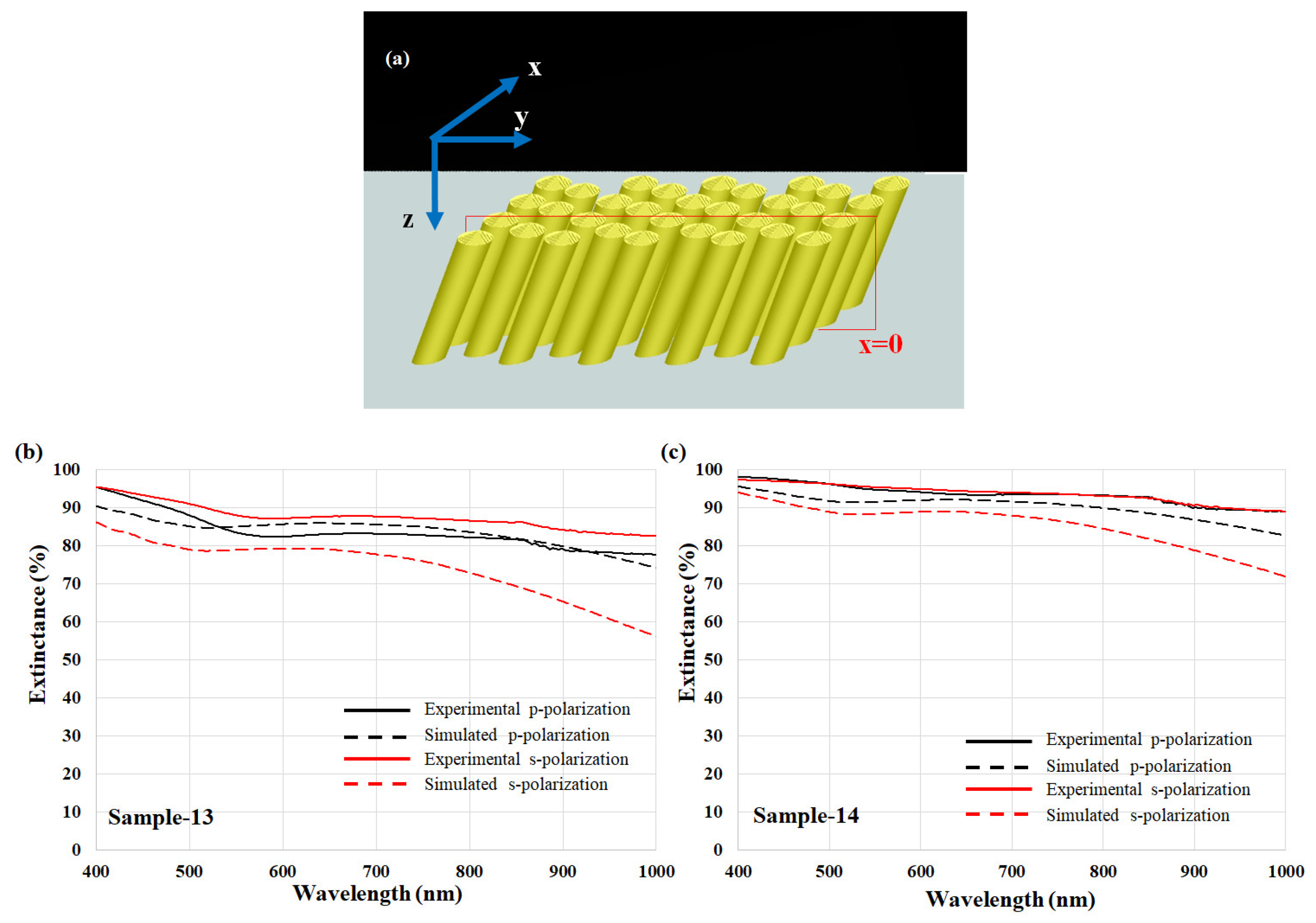
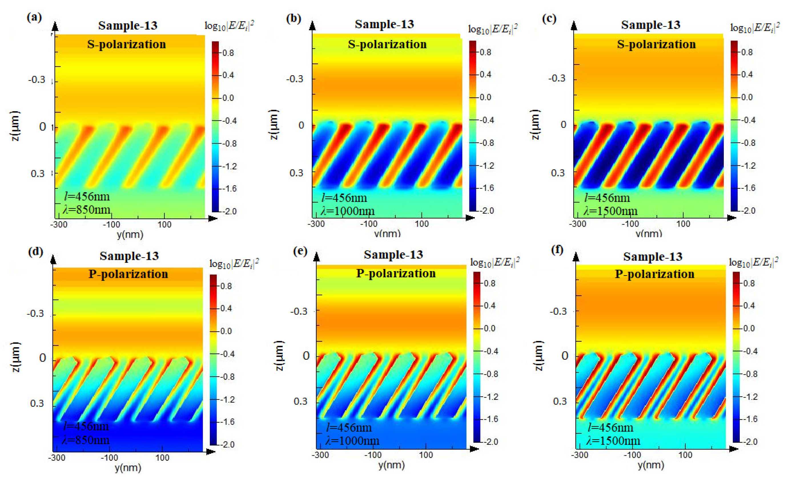
To gain insight into the broadening of the extinctance spectra, the electric field profiles of the TiN NRAs that were illuminated by s- and p-polarized light waves were simulated using the finite-difference time-domain (FDTD) (Lumerical FDTD Solutions 8.11.337) method. The following parameters were used in the simulations: FDTD cell size Δx = Δy = Δz = 2 nm, and the time step Δt = 0.95/c(Δx2 + Δy2 + Δz2)−0.5, where c is the speed of light, chosen according to the Courant stability criterion. The (x, y, z) coordinate system is oriented as in Figure 10a. According to the SEM of TiN NRA in this work, the surface roughness of the rod is less than 10 nm, which is much smaller than the wavelength. In a previous work, the polycrystalline TiN thin films were routinely fabricated by magnetron sputtering with a substrate temperature in the range of 300–600 K [29]. Our deposition condition would lead to polycrystalline structures. The refractive index of polycrystalline TiN was utilized in the simulations. The optical constants of the TiN film were taken from Sample-2. The TiN nanorods were arranged consistent with the morphologies of Sample-13 and Sample-14. Two slanted NRAs with rod lengths of 456 and 730 nm were simulated. Light waves with s- and p-polarization are normally incident onto the TiN NRA; the electric field intensity is defined as |E/Ei|2, where Ei and E are the amplitudes of the incident electric field and the localized electric field, respectively. The arrangement of TiN NRA is according to the morphology from SEM for simulation. Figure 10 also shows the simulated and measured extinctance spectra. The average difference between simulated extinctance and measured extinctance over wavelengths from 400 to 1000 nm is 7.1% for Sample-13 and 0.1% for Sample-14. Figure 11 plots the electric field intensity distributions in cross-sections (y–z plane) at x = 0 on a logarithmic scale. The electric field intensities were calculated at three wavelengths: 850, 1000, and 1500 nm. The field intensity distributions in the cross-sections reveal the mechanism of light absorption. For s-polarization, the strong electric field is localized in narrow gaps between TiN nanorods. The field in the gap is strongest close the surface. As the wavelength increases, the field enhancement extends deeper. Therefore, longer nanorods support more hot spots in the gaps. The field intensity at the bottom of 456 nm long nanorods is higher than that at the bottom of 730 nm long nanorods, indicating that the transmission decreases as the length of the rods increases, so the extinction of the NRA increases with the length of the rods. For p-polarization, the electric field is strong on the lateral surface of each nanorod. For 456 nm long rods, the field is strong from the top to the bottom and the hot spots extend to the bottom of the NRA, causing the transmission of light through the sample. For the 730 nm long rods, the field is strong from the top to a depth of 500 nm (z = 500 nm). Therefore, the field intensity at the bottom is extremely low, so transmission is low and the extinction is high.
3. Conclusions
Slanted TiN NRA were grown by self-shadowing in a DC reactive magnetron sputtering system. The morphology of the obliquely deposited TiN NRA was varied by varying the deposition angle and by limiting the vapor flux. The transverse and longitudinal plasmonic modes of the TiN NRA cause strong extinction within different ranges of wavelengths and angles of incidence. The s-polarized extinctance spectra reveal strong extinction, corresponding to the transverse plasmonic mode around a wavelength of 400 nm. The p-polarized extinctance spectra reveal strong extinction that corresponds to both plasmonic modes and one strong extinction peak that corresponds to a longitudinal plasmonic mode at a wavelength of around 870 nm. The red-shift of the extinctance peak wavelength with increasing rod length was measured. The high extinction bands in both modes are larger than those of the silver nanorod array and the high extinction band is extended as the rods become longer. Because of the high extinction, a TiN NRA with a thickness of over 426 nm exhibits broad band and wide-angle light extinction. The near-field simulation indicates that localized surface plasmon resonances support the broadening of the high extinction band with increasing length of the rods. Based on this work, the TiN NRA as a plasmonic nanostructure can be mass-produced by GLAD and the tunable localized field enhancement can be applied to surface-enhanced Raman scattering sensing, bio-therapy, and thermophotovoltaic devices.
Author Contributions
Conceptualization, Y.-J.J.; Methodology, Y.-J.J. and M.-J.L.; Software, W.-C.W. and K.-L.W.; Validation, Y.-J.J. and M.-J.L.; Formal Analysis, W.-C.W. and K.-L.W.; Investigation, Y.-J.J. and M.-J.L.; Resources, Y.-J.J.; Data Curation, W.-C.W. and K.-L.W.; Writing–Original Draft Preparation, Y.-J.J.; Writing–Review & Editing, Y.-J.J. and M.-J.L.; Visualization, W.-C.W. and K.-L.W.; Supervision, Y.-J.J.; Project Administration, Y.-J.J.; Funding Acquisition, Y.-J.J.
Funding
This research was funded by Ministry of Science and Technology of the Republic of China, Taiwan (No. MOST 105-2221-E-027-072-MY3).
Acknowledgments
The authors acknowledge BoHuei Liao (associate researcher, Instrument technology research center, Taiwan) for providing counsel in the experiment.
Conflicts of Interest
The authors declare no conflict of interest.
References
- Stewart, M.E.; Anderton, C.R.; Thompson, L.B.; Maria, J.; Gray, S.K.; Rogers, J.A.; Nuzzo, R.G. Nanostructured plasmonic sensors. Chem. Rev. 2008, 108, 494–521. [Google Scholar] [CrossRef] [PubMed]
- Boltasseva, A.; Nikolajsen, T.; Leosson, K.; Kjaer, K.; Larsen, M.S.; Bozhevolnyi, S.I. Integrated optical components utilizing long-range surface plasmon polaritons. J. Lightwave Technol. 2005, 23, 413. [Google Scholar] [CrossRef]
- Challener, W.A.; Peng, C.; Itagi, A.V.; Karns, D.; Peng, W.; Peng, Y.; Yang, X.; Zhu, X.; Gokemeijer, N.J.; Hsia, Y.-T. Heat-assisted magnetic recording by a near-field transducer with efficient optical energy transfer. Nat. Photonics 2009, 3, 220. [Google Scholar] [CrossRef]
- Naik, G.V.; Kim, J.; Boltasseva, A. Oxides and nitrides as alternative plasmonic materials in the optical range. Opt. Mater. Express 2011, 1, 1090–1099. [Google Scholar] [CrossRef]
- Guler, U.; Naik, G.V.; Boltasseva, A.; Shalaev, V.M.; Kildishev, A.V. Performance analysis of nitride alternative plasmonic materials for localized surface plasmon applications. Appl. Phys. B 2012, 107, 285–291. [Google Scholar] [CrossRef]
- Guler, U.; Shalaev, V.M.; Boltasseva, A. Nanoparticle plasmonics: Going practical with transition metal nitrides. Mater. Today 2015, 18, 227–237. [Google Scholar] [CrossRef]
- Guler, U.; Boltasseva, A.; Shalaev, V.M. Refractory plasmonics. Science 2014, 344, 263–264. [Google Scholar] [CrossRef]
- Boltasseva, A.; Atwater, H.A. Low-loss plasmonic metamaterials. Science 2011, 331, 290–291. [Google Scholar] [CrossRef]
- Pierson, H.O. Handbook of Refractory Carbides & Nitrides: Properties, Characteristics, Processing and Applications; William Andrew Inc.: Norwich, NY, USA, 1996. [Google Scholar]
- Wang, H.; Chen, Q.; Wen, L.; Song, S.; Hu, X.; Xu, G. Titanium-nitride-based integrated plasmonic absorber/emitter for solar thermophotovoltaic application. Photonics Res. 2015, 3, 329–334. [Google Scholar] [CrossRef]
- Li, W.; Guler, U.; Kinsey, N.; Naik, G.V.; Boltasseva, A.; Guan, J.; Shalaev, V.M.; Kildishev, A.V. Refractory plasmonics with titanium nitride: Broadband metamaterial absorber. Adv. Mater. 2014, 26, 7959–7965. [Google Scholar] [CrossRef]
- Guler, U.; Suslov, S.; Kildishev, A.V.; Boltasseva, A.; Shalaev, V.M. Colloidal plasmonic titanium nitride nanoparticles: Properties and applications. Nanophotonics 2015, 4, 269–276. [Google Scholar] [CrossRef]
- He, W.; Ai, K.; Jiang, C.; Li, Y.; Song, X.; Lu, L. Plasmonic titanium nitride nanoparticles for in vivo photoacoustic tomography imaging and photothermal cancer therapy. Biomaterials 2017, 132, 37–47. [Google Scholar] [CrossRef] [PubMed]
- Wei, H.; Wu, M.; Dong, Z.; Chen, Y.; Bu, J.; Lin, J.; Yu, Y.; Wei, Y.; Cui, Y.; Wang, R. Composition, microstructure and SERS properties of titanium nitride thin film prepared via nitridation of sol-gel derived titania thin films. J. Raman Spectrosc. 2017, 48, 578–585. [Google Scholar] [CrossRef]
- Kaisar, N.; Huang, Y.-T.; Jou, S.; Kuo, H.-F.; Huang, B.-R.; Chen, C.-C.; Hsieh, Y.-F.; Chung, Y.-C. Surface-enhanced Raman scattering substrates of flat and wrinkly titanium nitride thin films by sputter deposition. Surf. Coat. Technol. 2018, 337, 434–438. [Google Scholar] [CrossRef]
- Zhao, J.; Lin, J.; Wei, H.; Li, X.; Zhang, W.; Zhao, G.; Bu, J.; Chen, Y. Surface enhanced Raman scattering substrates based on titanium nitride nanorods. Opt. Mater. 2015, 47, 219–224. [Google Scholar] [CrossRef]
- Ban, R.; Yu, Y.; Zhang, M.; Yin, J.; Xu, B.; Wu, D.-Y.; Wu, M.; Zhang, Z.; Tai, H.; Li, J.; et al. Synergetic SERS Enhancement in a metal-like/metal double-shell structure for sensitive and stable application. ACS Appl. Mater. Interfaces 2017, 9, 13564–13570. [Google Scholar] [CrossRef] [PubMed]
- Mumtaz, A.; Class, W.H. Color of titanium nitride prepared by reactive dc magnetron sputtering. J. Vac. Sci. Technol. 1982, 20, 345–348. [Google Scholar] [CrossRef]
- Håkansson, G.; Hultman, L.; Sundgren, J.-E.; Greene, J.E.; Münz, W.-D. Microstructures of TiN films grown by various physical vapour deposition techniques. Surf. Coat. Technol. 2000, 48, 51–67. [Google Scholar] [CrossRef]
- Ali, M.; Hamzah, E.; Qazi, I.A.; Toff, M.R.M. Effect of cathodic arc PVD parameters on roughness of TiN coating on steel substrate. Cur. App. Phys. 2010, 10, 471–474. [Google Scholar] [CrossRef]
- Ramaseshan, R.; Jose, F.; Rajagopalan, S.; Dash, S. Preferentially oriented electron beam deposited TiN thin films using focused jet of nitrogen gas. Surf. Eng. 2016, 32, 834–839. [Google Scholar] [CrossRef]
- Robbie, K.; Sit, J.C.; Brett, M.J. Advanced techniques for glancing angle deposition. J. Vac. Sci. Technol. B 1998, 16, 1115–1122. [Google Scholar] [CrossRef]
- Jen, Y.-J.; Lakhtakia, A.; Yu, C.-W.; Jhou, J.-J.; Wang, W.-H.; Lin, M.-J.; Wu, H.-M.; Liao, H.-S. Silver/silicon dioxide/silver sandwich films in the blue-to-red spectral regime with negative-real refractive index. Appl. Phys. Lett. 2011, 99, 181117. [Google Scholar] [CrossRef]
- Hodgkinson, I.J.; Wu, Q. Birefringent Thin Films and Polarizing Elements; World Scientific: Singapore, 1998. [Google Scholar]
- Jen, Y.-J.; Lakhtakia, A.; Yu, C.-W.; Lin, C.-F.; Lin, M.-J.; Wang, S.-H.; Lai, J.-R. Biologically inspired achromatic waveplates for visible light. Nat. Commun. 2011, 2, 363. [Google Scholar] [CrossRef] [PubMed] [Green Version]
- Jen, Y.-J.; Lakhtakia, A.; Lin, M.-J.; Wang, W.-H.; Wu, H.-M.; Liao, H.-S. Metal/dielectric/metal sandwich film for broadband reflection reduction. Sci. Rep. 2013, 3, 1672. [Google Scholar] [CrossRef] [PubMed] [Green Version]
- Guler, U.; Zemlyanov, D.; Kim, J.; Wang, Z.; Chandrasekar, R.; Meng, X.; Stach, E.; Kildishev, A.V.; Shalaev, V.M.; Boltasseva, A. Plasmonic titanium nitride nanostructures via nitridation of nanopatterned titanium dioxide. Adv. Opt. Mater. 2017, 5, 1600717. [Google Scholar] [CrossRef]
- Backholm, M.; Foss, M.; Nordlund, K. Roughness of glancing angle deposited titanium thin films: An experimental and computational study. Nanotechnology 2012, 23, 385708. [Google Scholar] [CrossRef] [PubMed]
- Xie, Z.; Liu, X.; Wang, W.; Liu, C.; Li, Z.; Zhang, Z. Fabrication of TiN nanostructure as a hydrogen peroxide sensor by oblique angle deposition. Nanoscale Res. Lett. 2014, 9, 105. [Google Scholar] [CrossRef] [PubMed] [Green Version]
- Bouaouina, B.; Mastail, C.; Besnard, A.; Mareus, R.; Nita, F.; Michel, A.; Abadias, G. Nanocolumnar TiN thin film growth by oblique angle sputter-deposition: Experiments vs. simulations. Mater. Des. 2018, 160, 338–349. [Google Scholar] [CrossRef]
- Ponon, N.K.; Appleby, D.J.; Arac, E.; King, P.; Ganti, S.; Kwa, K.S.; O’Neill, A. Effect of deposition conditions and post deposition anneal on reactively sputtered titanium nitride thin films. Thin Solid Films 2015, 578, 31–37. [Google Scholar] [CrossRef]
- Shah, D.; Reddy, H.; Kinsey, N.; Shalaev, V.M.; Boltasseva, A. Optical properties of plasmonic ultrathin TiN Films. Adv. Opt. Mater. 2017, 5, 1700065. [Google Scholar] [CrossRef]
- Jen, Y.-J.; Lin, Y.W.; Huang, Y.-J.; Chan, T.-L. The effect of glancing angle deposition conditions on the morphology of a silver nanohelix array. Coatings 2017, 7, 140. [Google Scholar] [CrossRef]
- Vick, D.; Friedrich, L.; Dew, S.; Brett, M.; Robbie, K.; Seto, M.; Smy, T. Self-shadowing and surface diffusion effects in obliquely deposited thin films. Thin Solid Films 1999, 339, 88–94. [Google Scholar] [CrossRef]
- Dick, B.; Brett, M.J.; Smy, T.; Belov, M.; Freeman, M.R. Periodic submicrometer structures by sputtering. J. Vac. Sci. Technol. B 2001, 19, 1813–1819. [Google Scholar] [CrossRef]
- Zhao, Y.-P.; Chaney, S.B.; Zhang, Z.-Y. Absorbance spectra of aligned Ag nanorod arrays prepared by oblique angle deposition. J. Appl. Phys. 2006, 100, 063527. [Google Scholar] [CrossRef]
- Leem, J.W.; Yu, J.S. Multi-functional antireflective surface-relief structures based on nanoscale porous germanium with graded refractive index profiles. Nanoscale 2013, 5, 2520–2526. [Google Scholar] [CrossRef] [PubMed]
- Jang, S.J.; Song, Y.M.; Yu, J.S.; Yeo, C.I.; Lee, Y.T. Antireflective properties of porous Si nanocolumnar structures with graded refractive index layers. Opt. Lett. 2011, 36, 253–255. [Google Scholar] [CrossRef] [PubMed]
Figure 1.
Schematic deposition system with Ar as sputtering gas and N2 as reactive gas.

Figure 2.
Cross-section and top-view scanning electron microscopic (SEM) images of titanium nitride (TiN) thin films.
Figure 2.
Cross-section and top-view scanning electron microscopic (SEM) images of titanium nitride (TiN) thin films.

Figure 3.
(a–c) Ti 2p and (d–f) N 1s photoemission core level spectra of TiN thin films; (g–i) X-ray diffraction by TiN thin films.
Figure 3.
(a–c) Ti 2p and (d–f) N 1s photoemission core level spectra of TiN thin films; (g–i) X-ray diffraction by TiN thin films.

Figure 4.
(a) The real and (b) imaginary part of permittivity for TiN thin films with RN2 = 1.5 sccm, RN2 = 3.5 sccm, and RN2 = 5 sccm.
Figure 4.
(a) The real and (b) imaginary part of permittivity for TiN thin films with RN2 = 1.5 sccm, RN2 = 3.5 sccm, and RN2 = 5 sccm.

Figure 5.
Top-view and cross-section scanning electron microscopic (SEM) images of TiN nanorod arrays (NRAs) deposited at α of (a) 75°, (b) 80°, (c) 85°, (d) 88° without flux collimation and at α of (e) 80°, (f) 85°, (g) 88° with flux collimation.
Figure 5.
Top-view and cross-section scanning electron microscopic (SEM) images of TiN nanorod arrays (NRAs) deposited at α of (a) 75°, (b) 80°, (c) 85°, (d) 88° without flux collimation and at α of (e) 80°, (f) 85°, (g) 88° with flux collimation.

Figure 6.
Top-view and cross-section scanning electron microscopic (SEM) images of TiN NRAs deposited at α = 85° with length of rod l equal to (a) 283 nm, (b) 348 nm, (c) 456 nm, and (d) 730 nm.
Figure 6.
Top-view and cross-section scanning electron microscopic (SEM) images of TiN NRAs deposited at α = 85° with length of rod l equal to (a) 283 nm, (b) 348 nm, (c) 456 nm, and (d) 730 nm.

Figure 7.
Measured (a–d) s-polarized and (e–h) p-polarized extinctance versus wavelength and angle of incidence for TiN NRA. Plane of incidence and the incident angle of θ are shown.
Figure 7.
Measured (a–d) s-polarized and (e–h) p-polarized extinctance versus wavelength and angle of incidence for TiN NRA. Plane of incidence and the incident angle of θ are shown.

Figure 8.
Measured s-polarized (a–d) reflectance and (e–h) transmittance versus wavelength and angle of incidence for TiN NRA.
Figure 8.
Measured s-polarized (a–d) reflectance and (e–h) transmittance versus wavelength and angle of incidence for TiN NRA.

Figure 9.
Measured p-polarized (a–d) reflectance and (e–h) transmittance versus wavelength and angle of incidence for TiN NRA.
Figure 9.
Measured p-polarized (a–d) reflectance and (e–h) transmittance versus wavelength and angle of incidence for TiN NRA.
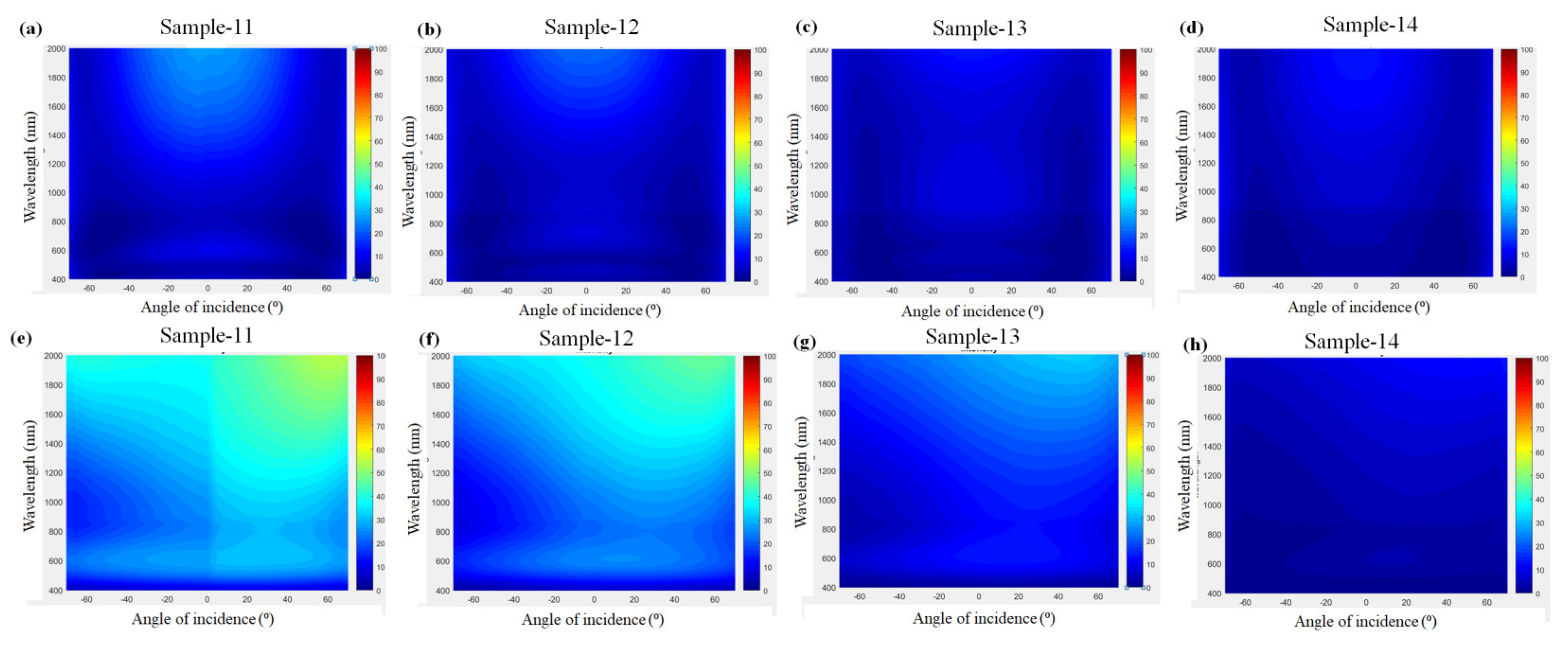
Figure 10.
(a) Schematic TiN NRA used in the simulation. Simulated extinctance and measured extinctance of (b) Sample-13 and (c) Sample-14 for s- and p-polarization.
Figure 10.
(a) Schematic TiN NRA used in the simulation. Simulated extinctance and measured extinctance of (b) Sample-13 and (c) Sample-14 for s- and p-polarization.

Figure 11.
Simulated electric field intensities of (a–f) 456 nm long nanorods and (g–l) 730 nm long nanorods in cross-sections (x = 0) at incident wavelengths of 850, 1000, and 1500 nm for s- and p-polarization.
Figure 11.
Simulated electric field intensities of (a–f) 456 nm long nanorods and (g–l) 730 nm long nanorods in cross-sections (x = 0) at incident wavelengths of 850, 1000, and 1500 nm for s- and p-polarization.


Table 1.
Average deposition angle (α), tilt angle (β), rod width (w), length of rod (l), spacing between adjacent rods (p), porosity, and thicknesses (d) of titanium nitride (TiN) nanorod arrays (NRAs).
Table 1.
Average deposition angle (α), tilt angle (β), rod width (w), length of rod (l), spacing between adjacent rods (p), porosity, and thicknesses (d) of titanium nitride (TiN) nanorod arrays (NRAs).
| TiN Nanorod Arrays | α (°) | β (°) | w (nm) | l (nm) | p (nm) | d (nm) | Porosity (%) |
|---|---|---|---|---|---|---|---|
| Sample-4 | 75 | 18.4 | 34.3 | 374 | 18.8 | 463 | 11.3 |
| Sample-5 | 80 | 17.9 | 40.5 | 470 | 19.1 | 400 | 14.7 |
| Sample-6 | 85 | 18.6 | 54.9 | 364 | 22.4 | 322 | 18.4 |
| Sample-7 | 88 | 18.5 | 55.5 | 359 | 24.2 | 314 | 21.7 |
| Sample-8 | 80 | 37.4 | 18.4 | 79.9 | 17.2 | 97 | 26.5 |
| Sample-9 | 85 | 38.6 | 27.5 | 87.3 | 20.4 | 73 | 27.6 |
| Sample-10 | 88 | 39.1 | 24.2 | 56.7 | 19.6 | 56 | 28.1 |
| Sample-11 | 85 | 18.4 | 57.8 | 283 | 11.7 | 267 | 16.8 |
| Sample-12 | 85 | 18.5 | 62.6 | 348 | 13.5 | 329 | 18.4 |
| Sample-13 | 85 | 18.6 | 66.7 | 456 | 15.5 | 426 | 19.5 |
| Sample-14 | 85 | 18.5 | 93.7 | 730 | 21.6 | 690 | 23.7 |
© 2018 by the authors. Licensee MDPI, Basel, Switzerland. This article is an open access article distributed under the terms and conditions of the Creative Commons Attribution (CC BY) license (http://creativecommons.org/licenses/by/4.0/).
Share and Cite
MDPI and ACS Style
Jen, Y.-J.; Wang, W.-C.; Wu, K.-L.; Lin, M.-J. Extinction Properties of Obliquely Deposited TiN Nanorod Arrays. Coatings 2018, 8, 465. https://doi.org/10.3390/coatings8120465
AMA Style
Jen Y-J, Wang W-C, Wu K-L, Lin M-J. Extinction Properties of Obliquely Deposited TiN Nanorod Arrays. Coatings. 2018; 8(12):465. https://doi.org/10.3390/coatings8120465
Chicago/Turabian StyleJen, Yi-Jun, Wei-Chien Wang, Kai-Lun Wu, and Meng-Jie Lin. 2018. "Extinction Properties of Obliquely Deposited TiN Nanorod Arrays" Coatings 8, no. 12: 465. https://doi.org/10.3390/coatings8120465
Note that from the first issue of 2016, this journal uses article numbers instead of page numbers. See further details here.