Effect of Substrate Temperature on the Optical and Electrical Properties of Nitrogen-Doped NiO Thin Films

1
Key Lab of Advanced Transducers and Intelligent Control System, Ministry of Education and Shanxi Province, Taiyuan University of Technology, Taiyuan 030024, China
2
College of Physics and Optoelectronics, Taiyuan University of Technology, Taiyuan 030024, China
3
First Design and Research Institute, China Wuzhou Engineering Group Corporation LTD, Beijing 100053, China
*
Authors to whom correspondence should be addressed.
Coatings 2019, 9(10), 634; https://doi.org/10.3390/coatings9100634
Submission received: 21 August 2019
/
Revised: 23 September 2019
/
Accepted: 26 September 2019
/
Published: 2 October 2019
(This article belongs to the Special Issue Advanced Thin Films Deposited by Magnetron Sputtering)
Abstract
:NiO is a widely used p-type semiconductor. The desired optical and electrical properties of NiO vary in different application fields. To modulate the properties of NiO, nitrogen (N)-doped NiO thin films were synthesized by reactive radio-frequency magnetron sputtering on ITO-coated glass substrates. The influence of substrate temperature on the properties of NiO was investigated. XRD studies indicated a cubic structure. With the increase of the substrate temperature, the average transmittance in the visible region gradually reduced from 90% to 50%. The bandgap energy narrowed from 3.5 to 3.08 eV. The intensity of the PL spectra weakened, and the electrical conductivity rose. Overall, changing the substrate temperature is an effective method to modulate the optical and electrical properties of N-doped NiO thin films.
1. Introduction
As a promising metal-oxide material in the semiconductor field, NiO has attracted a lot of attention in recent years. NiO is a wide-bandgap p-type semiconductor applied as a transparent conducting film [1], electrode in electrochromic devices [2], and functional layer for chemical sensors [3]. These applications strongly depend on its optical and electrical properties. Therefore, it is crucial to modulate the optical and electrical properties of NiO thin films to exploit its applications. There are many methods to fabricate NiO thin films, such as chemical vapor deposition [4], facile sol-gel synthesis [5], magnetron sputtering [6], spray pyrolysis [7], and pulsed laser deposition [8]. Among them, magnetron sputtering is the most used, with the advantages of high quality, good adhesion, low growth temperature, and high efficiency [9]. In general, changing the deposition conditions, heating treatment, and doping is effective to regulate the optical and electrical properties of NiO thin films. Many studies report the variation of NiO thin films’ properties with the deposition conditions. Nandy et al. [10] studied the effect of oxygen partial pressure on the electrical and optical properties of NiO thin films. The electrical conductivity and transparency decreased with increasing oxygen partial pressure. Meanwhile, the bandgap narrowed. Sato [11] observed a gradual increase of resistivity with the increasing of substrate temperature. The influence of the heating treatment was studied as well. The resistivity increased with heating, while the transparency increased gradually from 40% to 80% as the temperature increased from 100 to 400 °C and then decreased to 60% when the temperature reached 500 °C. Considering the small adjustments possible for deposition conditions and heating treatment to modulate NiO properties, doping was identified as the most effective approach. Al-doped NiO showed enhanced electrical conductivity [12]. On the contrary, Li-doped NiO displayed significantly decreased electrical conductivity. In 2017, Keraudy [13] deposited N-doped NiO thin films on a Ni metal target by mixing reactive N2 and O2 to non-reactive Argon. The influence of the N/O rate on the optical and electrical properties was studied. However, as the O content has a strong impact on the properties of NiO thin films, the result obtained actually was due to the synergistic effects of N doping and the change of O content. In this paper, N-doped NiO thin films were grown on a NiO ceramic target by mixing N2 to Argon. To modulate the properties of the N-doped NiO thin film, the evolution of the optical and electrical properties with substrate temperature was investigated.
2. Materials and Methods
NiO thin films were deposited by reactive radio-frequency magnetron sputtering onto commercially purchased ITO (sheet resistance value: 20 Ω/cm, size: 2 cm × 2 cm)-coated glass substrates. The substrates were cleaned with soapy water, alcohol, and deionized water successively. A NiO ceramic target (99.99% purity) of 6 cm in diameter and 3 mm in thickness was used. The base pressure was 2 × 10⁻⁵ Pa, and the working pressure was 1 Pa. The sputter power was kept at 60 W. The distance between target and substrate was 5 cm and remained constant throughout the sputtering process. An undoped NiO thin film was deposited using Ar at room temperature. N-doped NiO thin films were deposited in the presence of 20% Ar/80% N2, at different substrate temperatures, i.e., room temperature, 100, 200, 300 and 400 °C. The thickness of the films was 300 nm, detected by an INFICON STM-2XM thickness monitor (Bad Ragaz, Switzerland).
The surface morphologies of the resulting films were observed by field emission scanning electron microscopy (FE-SEM: Hitachi S4800) and atomic force microscopy (AFM: NT-MDT Prima, Moscow, Russia). An X-ray diffractometer (Philips X’pert PRO, Amsterdam, Netherlands) equipped with Cu Kα radiation was adopted to analyze the structure. Room-temperature Raman spectroscopy was carried out by a Renishaw Raman spectrometer using a 532 nm solid-state laser as the excitation source. X-ray photoelectron spectroscopy (XPS) measurements were performed by Thermo ESCALAB 250XI (Waltham, MA, USA) with Al Kα radiation. UV–Vis transmittance spectra were obtained by a spectrofluorometer (FS5-Edinburgh Instruments, Livingston, UK). Room-temperature photoluminescence (PL) was performed with a 325 nm He–Cd laser as the excitation source. The Mott–Schottky plots were obtained in a three-electrode glass cell using a 0.5 M Na2SO4 aqueous solution connected to an electrochemical workstation (CHI760E, Beijing Huake Putian technology limited liability company, Beijing, China). A platinum electrode and an Ag/AgCl electrode were selected to be the counter electrode and the reference electrode, respectively. The impedance of NiO thin films was measured in an electrochemical workstation. The two electrodes were connected with the impedance measuring system, as shown in Figure 1. During measurement, a = 1 cm, b = 2 cm.
3. Results
Table 1 reports the deposition rate as a function of the substrate temperature. The deposition rate slightly increased with the substrate temperature. Although the target was cooled by running water, the temperature of the target surface increased as the substrate temperature increased, which resulted in an increase of the activation energy of atoms and then an increase of the sputtering rate.
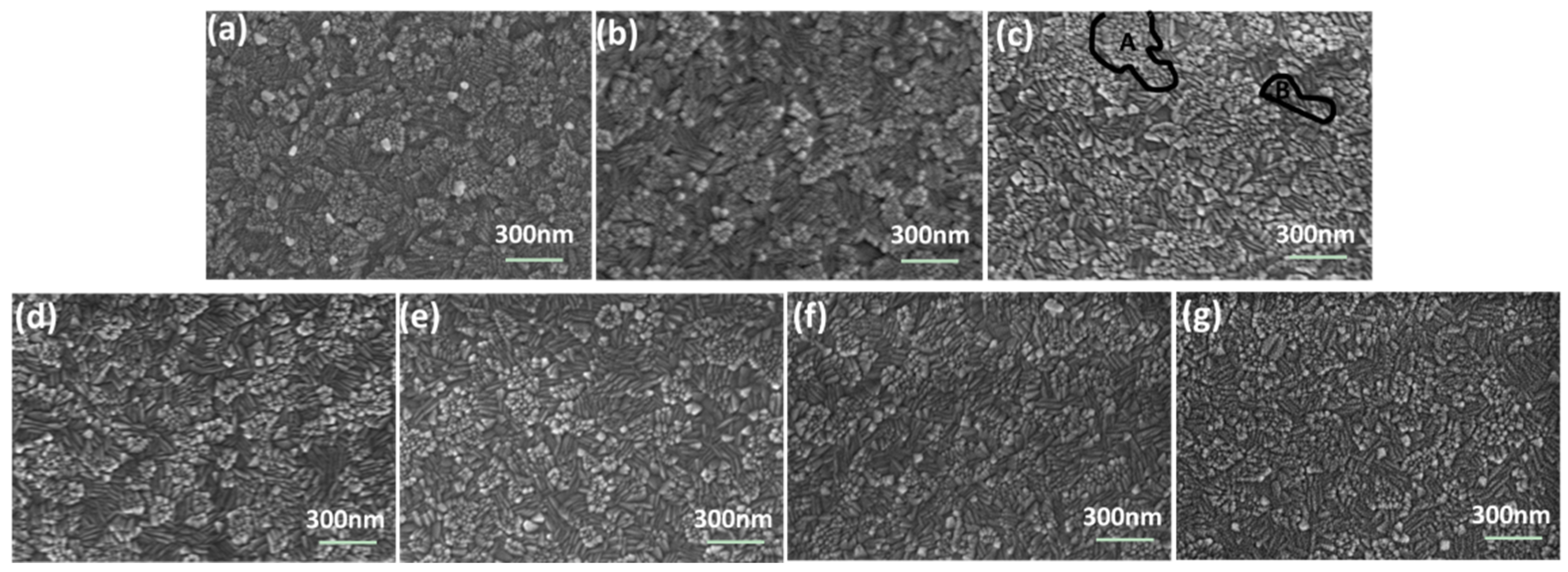
Figure 2 shows the surface morphologies of ITO, undoped NiO, and N-doped NiO thin films deposited at different substrate temperatures. All NiO samples were poly-crystalline films with grain–subgrain structure, owing to the impact of the grain–subgrain structure of ITO (Figure 2a). Grains were distributed into highly oriented regions. Region A was composed of squares subgrains, while region B consisted of bar-type subgrains. Compared with undoped NiO films (Figure 2b), N-doped NiO films (Figure 2c) were looser, owing to the negative effect of N2 on film quality during magnetron sputtering. According to Figure 2c–g, with the increase of substrate temperature, region A shrank and region B increases. Meanwhile, the subgrains became sags and crests. By changing the focus of SEM, it was revealed that the thickness of region A was greater than that of region B.
To determine the thickness difference between region A and region B of NiO thin films, AFM measurements were performed. Figure 3a shows an AFM surface image (1 × 1 μm2 scan area) of an N-doped NiO thin film at room temperature. Figure 3b illustrates the thickness variation along the line in Figure 3a. According to Figure 3b, region A was 9 nm thicker than region B, on average.
Figure 4a shows the XRD spectra of NiO thin films at different substrate temperatures. The XRD spectra indicated a cubic NiO phase. However, according to the literature, at temperatures above the Néel temperature (523 K), the crystal structure of NiO is cubic, whereas below the Néel temperature, the crystals become slightly distorted from this cubic structure and acquire a rhombohedral structure which accompanies the antiferromagnetic ordering [14,15]. The difference between the angles of the rhombohedral and the fcc NiO was very small, due to the broadening of the peaks, and no difference appeared in the XRD spectra. The diffraction peaks around 37.2° and 41.2° were assigned to NiO (111) and NiO (200), while the others are characteristic of the ITO layers [16]. Diffraction peaks of (220) at 62.9° and (311) at 75.4° were not visible, which indicated a preferred orientation of the NiO thin films. As seen in Figure 4b, the (111) peak position of undoped and N-doped NiO thin films is the same. The (111) peak shifted towards a higher angle as the temperature increased from room temperature to 400 °C, corresponding to a smaller interplanar spacing, as shown in Figure 4c.
The room-temperature Raman scattering spectra of NiO thin films at different substrate temperatures are shown in Figure 5. Four peaks were observed. Raman peaks located at about 458 and 599 cm−1 corresponded to the transverse optical (TO) and longitudinal optical (LO) phonon modes of NiO, respectively. It was suggested that the appearance of LO phonon may be due to Ni vacancy defects [17,18,19]. Two other peaks, at 783 and 1100 cm−1, were assigned to two-phonon scattering 2TO and 2LO, respectively. These results further proved the crystalline structure of NiO.
The surface elemental composition and state of NiO thin films were analyzed by XPS, as shown in Figure 6. The XPS survey spectra in Figure 6a show the peaks characteristics of nickel, oxygen, nitrogen, and carbon in all samples. The Ni 2p spectra (Figure 6b) contained six components. The peaks at 853.9 and 872.8 eV were attributed to Ni2+, and the peak at around 861.1 eV is their satellite (sat.) peak. The peak at 855.7 eV was assigned to Ni3+ [20]. A shakeup-type satellite peak of Ni 2p1/2 was detected at 879.7 eV. The O 1s spectra shown in Figure 6c contain two peaks at 529.6 and 531.4 eV, corresponding to Ni–O and Ni2O3 [21]. N 1s spectra are shown in Figure 6d. The peaks located at 396.7 and 397.8 eV were assigned to atomic N in Ni oxide lattice [22] and N atom bonded to O [23], respectively. The other two peaks at 400.2 and 402.0 eV could be attributed to nitrogen atoms related to N–O bonds due to surface oxidation and ammonium-type bonds [24,25,26].
The N 1s spectra of NiO films deposited at different substrate temperatures are shown in Figure 7a. For undoped NiO films, the absence of peaks located at 396.7 and 397.8 eV indicated that no N was incorporated into NiO films. The peaks at 396.7 and 397.8 eV appeared when N2 was adopted as the reactive gas. However, these two peaks were very weak at room temperature, corresponding to the small content of N in NiO. As the substrate temperature increased, the peaks at 396.7 and 397.8 eV became obvious, and the area of these two peaks increased. According to Figure 7a, the N content in NiO films increased with the substrate temperature. The content of N on the surface of NiO films obtained from XPS is shown in Figure 7b. For undoped NiO films, N concentration was 2.17%, owing to surface N absorption. When N2 was adopted as the reactive gas, the N concentration increased slightly to 2.52%. With the substrate temperature increasing to 100, 200, 300 and 400 °C, N concentration on the surface of NiO increased to 2.71%, 3.34%, 3.39% and 4.20%.
The color of N-doped NiO thin films transformed from semitransparent grey to opaque dark brown as the substrate temperature varied from room temperature to 400 °C. Ni3+ is responsible to the coloring of NiO [27]. In fact, the incorporation of N in NiO is an endothermic reaction [28] (ΔHf > 0). This positive heat of formation indicates that N doping requires a net energy input. Heating provides external energy and promotes N doping. Thus, as the substrate temperature roses, the N content of the NiO thin films increased, and Ni3+ increased correspondingly.
UV–Vis transmittance spectra of NiO thin films are shown in Figure 8. The effect of the ITO layer and glass on the transmittance was deducted as baseline. The transmittance of NiO thin films at room temperature reduced slightly when N was doped. For N-doped NiO, the average transmittance in the visible region reduced from 90% to 50% gradually as the temperature increased from room temperature to 400 °C. The reduced transmittance was associated with the increase of Ni3+ [27]. The optical bandgap energy (Eg) of N-doped NiO thin films at different substrate temperatures is shown in Figure 4b. It was determined from the Tauc’s plot shown in the inset. The Tauc’s plot was calculated using the Tauc’s relation below:
where hv is the photon energy, B is a constant, Eg is the optical bandgap energy, and α is the absorption coefficient given by the relation:
where t is the film thickness, I is the transmitted intensity at a particular wavelength, and I0 is the incident intensity.
The optical bandgap energy of the films was evaluated by extrapolating the linear region to zero absorption coefficient from the Tauc plots. The bandgap energy value for undoped NiO thin films was 3.53 eV. The bandgap energy values for N-doped NiO thin films at room temperature, 100, 200, 300 and 400 °C were 3.5, 3.45, 3.38, 3.33 and 3.08 eV, respectively. According to reference [29], N-doping leads to bandgap narrowing. As N concentration increased with the temperature, the bandgap energy of N-doped NiO thin films decreased.
Mott–Schottky plots of NiO thin films (Figure 9a) were adopted to assess the valence band edge potential (EVB). Since the valence band edge potential practically coincides with the flat band potential for p-type semiconductors, the Mott–Schottky relation can be used as follows [30]:
where ε is the permittivity of the samples, ε0 is the permittivity of free space, e is the elementary charge, NA is the donor density, E is the applied potential, EFB is the flat band potential, k is the Boltzmann’s constant, T is the temperature of operation, and C is the space charge capacitance. The space charge capacitance was determined by measuring the electrochemical impedance. An AC-voltage signal with amplitude of 0.01 V was applied at 1000 Hz. The capacitance was calculated from the imaginary part of the measured impedance Zimag [30]:
The Mott–Schottky plots were constructed as a function of the applied DC potential. The Mott–Schottky plots of all samples were obtained using an Ag/AgCl electrode in 1 M NaSO4 aqueous solution. The Mott–Schottky plots showed a V shape curve revealing a p–n junction structure of ITO layer and NiO thin film. The Mott–Schottky plot of the ITO layer in Figure 9a exhibits a positive slope, confirming an n-type conductivity. According to Figure 9a, all N-doped NiO thin films were p-type semiconductors. The flat band potential EFB is the intercept of the plot linear part with the potential axis. The EFB of undoped NiO thin films versus the Ag/AgCl electrode was 0.75 V. The EFB of N-doped NiO thin films versus the Ag/AgCl electrode was 1.06, 1.13, 2.09, 1.9, 1.2 V as the substrate temperature increased from room temperature to 100, 200, 300 and 400 °C. EVB values were calculated according to the equation [31]:
where ΔE = 0.21 V is the Ag/AgCl potential against a normal hydrogen electrode (NHE).
The conduction band edge potential (ECB) values were calculated according to the equation [31]:
where Eg is the optical band gap energy obtained from UV–Vis transmittance spectra.
The calculated energy band diagrams are shown in Figure 9b. According to Figure 9b, the potential of the bands first downshifted and then upshifted with the increase of temperature. The potential of the bands was minimum at 200 °C.
According to Figure 10, the impedance of undoped NiO thin film was 28.3 Ω. The impedance of N-doped NiO thin films decreased from 28 to 27.5, 26, 21, 16 Ω as the temperature increased from room temperature to 100, 200, 300, 400 °C. As the electrical conductivity is inversely proportional to the impedance, the electrical conductivity improved with the increase of the temperature. According to the literature, the electrical conductivity is proportional to the transfer of positive charge from cation to cation through the lattice [32], i.e., [Ni3+]. With the increase of the temperature, [Ni3+] increased, thus the electrical conductivity increased.
Figure 11 presents the room temperature PL spectra of NiO thin films at different substrate temperatures. For all samples, a dominant near band edge (NBE) emission peak centered at 395 nm (3.14 eV) and a weak emission peak at 524 nm (2.37 eV) can be clearly seen. The NBE emission originates from the direct recombination of the excitons through exciton–exciton scattering [33]. The weak emission at 524 nm is attributed to the radiative recombination of a photo-generated hole with an electron occupying the nickel and oxygen vacancies [34]. Compared with undoped NiO thin films, it can be seen that the N-doped NiO thin films exhibited PL signals with a similar curve shape, demonstrating that N-doping did not give rise to new PL phenomena. Indeed, the dopant in a stable chemical state will not generate different PL phenomena, because it is unable to capture electrons. The PL intensity of NiO thin films decreased as the temperature rose from room temperature to 400 °C. It is thought that the difference of the emission intensity likely depends on morphology variations. [35]
4. Conclusions
N-doped NiO thin films at different substrate temperatures were prepared by radio-frequency reactive magnetron sputtering. The influence of substrate temperature on the optical and electronic properties was investigated. According to the research, the transmittance of N-doped NiO decreased with the increase of the substrate temperature. The energy band structure was determined by analyzing transmittance spectra and Mott–Schottky plots. The energy band gap shrank as the substrate temperature rose. The valence band edge potential and conduction edge potential increased when the substrate temperature increased from room temperature to 200 °C, then decreased as the substrate temperature continued to rise. The intensity of the PL spectra decreased and the conductivity increased.
Author Contributions
Conceptualization, Y.T.; Methodology, Y.T.; Software, Y.T.; Validation, Y.T., Y.Y. and X.Z.; Formal Analysis, Y.T.; Investigation, L.G.; Resources, Y.Y.; Data Curation, X.Q.; Writing—Original Draft Preparation, Y.T.; Writing—Review and Editing, Y.T.; Visualization, Y.T.; Supervision, Y.Y.; Project Administration, Y.T.; Funding Acquisition, Y.T.
Funding
This research was funded by the National Natural Science Foundation of China (No. 51702226) and the Natural Science Foundation of Shanxi Province (No. 201701D221078).
Conflicts of Interest
The authors declare no conflict of interest.
References
- Sasi, B.; Gopchandran, K.G.; Manoj, P.K.; Koshy, P.; Rao, P.P.; Vaidyan, V.K. Preparation of transparent and semiconducting NiO films. Vacuum 2002, 68, 149–154. [Google Scholar] [CrossRef]
- Liu, H.; Zheng, W.; Yan, X.; Feng, B. Studies on electrochromic properties of nickel oxide thin films prepared by reactive sputtering. J. Alloy. Compd. 2008, 462, 356–361. [Google Scholar] [CrossRef]
- Mahmoud, S.A.; Akl, A.A.; Kamal, H.; Abdel-Hady, K. Opto-structural, electrical and electrochromic properties of crystalline nickel oxide thin films prepared by spray pyrolysis. Physica B 2002, 311, 366–375. [Google Scholar] [CrossRef]
- Maruyama, T.; Arai, S. The electrochromic properties of nickel oxide thin films prepared by chemical vapor deposition. Sol. Energy Mater. Sol. Cells 1993, 30, 257–262. [Google Scholar] [CrossRef]
- Guo, W.; Hui, K.N.; Hui, K.S. High conductivity nickel oxide thin films by a facile sol-gel method. Mater. Lett. 2013, 92, 291–295. [Google Scholar] [CrossRef]
- Subramanian, B.; Ibrahim, M.M.; Senthilkumar, V.; Murali, K.R.; Vidhya, V.S.; Sanjeeviraja, C.; Jayachandran, M. Optoelectronic and electrochemical properties of nickel oxide (NiO) films deposited by DC reactive magnetron sputtering. Physica B 2008, 403, 4104–4110. [Google Scholar] [CrossRef]
- Ismail, R.A.; Ghafori, S.A.; Kadhim, G.A. Preparation and characterization of nanostructured nickel oxide thin films by spray pyrolysis. Appl. Nanosci. 2013, 3, 509–514. [Google Scholar] [CrossRef]
- Jahromi, S.P.; Huang, N.M.; Kamalianfar, A.; Lim, H.N.; Muhamad, M.R.; Yousefi, R. Facile synthesis of porous-structured nickel oxide thin film by pulsed laser deposition. J. Nanomater. 2012, 2012, 97. [Google Scholar] [CrossRef]
- Soo Kim, D.; Chul Lee, H. Nickel vacancy behavior in the electrical conductance of nonstoichiometric nickel oxide film. J. Appl. Phys. 2012, 112, 034504. [Google Scholar] [CrossRef]
- Nandy, S.; Saha, B.; Mitra, M.K.; Chattopadhyay, K.K. Effect of oxygen partial pressure on the electrical and optical properties of highly (200) oriented p-type Ni1−xO films by DC sputtering. J. Mater. Sci. Lett. 2007, 42, 5766–5772. [Google Scholar] [CrossRef]
- Sato, H.; Minami, T.; Takata, S.; Yamada, T. Transparent conducting p-type NiO thin films prepared by magnetron sputtering. Thin Solid Films 1993, 236, 27–31. [Google Scholar] [CrossRef]
- Nandy, S.; Maiti, U.N.; Ghosh, C.K.; Chattopadhyay, K.K. Enhanced p-type conductivity and band gap narrowing in heavily Al doped NiO thin films deposited by RF magnetron sputtering. J. Phys. 2009, 21, 115804. [Google Scholar] [CrossRef] [PubMed]
- Keraudy, J.; Ferrec, A.; Richard-Plouet, M.; Hamon, J.; Goullet, A.; Jouan, P.Y. Nitrogen doping on NiO by reactive magnetron sputtering: A new pathway to dynamically tune the optical and electrical properties. Appl. Surf. Sci. 2017, 409, 77–84. [Google Scholar] [CrossRef]
- Slack, G.A. Crystallography and domain walls in antiferromagnetic NiO crystals. J. Appl. Phys. 1960, 31, 1571–1582. [Google Scholar] [CrossRef]
- Roth, W.L. Neutron and optical studies of domains in NiO. J. Appl. Phys. 1960, 31, 2000–2011. [Google Scholar] [CrossRef]
- Qiu, J.; Chen, Z.; Zhao, T.; Chen, Z.; Chu, W.; Yuan, N.; Ding, J. Electrochromic Properties of NiOx Films Deposited by DC Magnetron Sputtering. J. Nanosci. Nanotechnol. 2018, 18, 4222–4229. [Google Scholar] [CrossRef] [PubMed]
- Ramasami, A.K.; Reddy, M.V.; Balakrishna, G.R. Combustion synthesis and characterization of NiO nanoparticles. Mater. Sci. Semicond. Process. 2015, 40, 194–202. [Google Scholar] [CrossRef]
- Zhu, H.; Dong, H.; Laveille, P.; Saih, Y.; Caps, V.; Basset, J.M. Metal oxides modified NiO catalysts for oxidative dehydro genation of ethaneto ethylene. Catal. Today 2014, 228, 58–64. [Google Scholar] [CrossRef]
- Mironova-Ulmane, N.; Kuzmin, A.; Grabis, J.; Sildos, I.; Voronin, V.I.; Berger, I.F.; Kazantsev, V.A. Structural and magnetic properties of nickel oxide nanopowder. Solid State Phenom. 2011, 168, 341–344. [Google Scholar] [CrossRef]
- Lei, Y.; Li, J.; Wang, Y.; Gu, L.; Chang, Y.; Yuan, H.; Xiao, D. Rapid microwave-assisted green synthesis of 3D hierarchical flower-shaped NiCo2O4 microsphere for high-performance supercapacitor. ACS Appl. Mater. Interfaces 2014, 6, 1773–1780. [Google Scholar] [CrossRef]
- Sasi, B.; Gopchandran, K.G. Nanostructured mesoporous nickel oxide thin films. Nanotechnology 2007, 18, 115613. [Google Scholar] [CrossRef]
- Asahi, R.; Morikawa, T.; Ohwaki, T.; Aoki, K.; Taga, Y. Visible-light photocatalysis in nitrogen-doped titanium oxides. Science 2001, 293, 269–271. [Google Scholar] [CrossRef] [PubMed]
- Wu, K.R.; Hung, C.H. Characterization of N, C-codoped TiO2 films prepared by reactive DC magnetron sputtering. Appl. Surf. Sci. 2009, 256, 1595–1603. [Google Scholar] [CrossRef]
- Aduru, S.; Contarini, S.; Rabalais, J.W. Electron-, X-ray-, and ion-stimulated decomposition of nitrate salts. J. Phys. Chem. 1986, 90, 1683–1688. [Google Scholar] [CrossRef]
- Simon, P.; Pignon, B.; Miao, B.; Coste-Leconte, S.; Leconte, Y.; Marguet, S.; Herlin-Boime, N. N-doped titanium monoxide nanoparticles with TiO rock-salt structure, low energy band gap, and visible light activity. Chem. Mater. 2010, 22, 3704–3711. [Google Scholar] [CrossRef]
- Duarte, D.A.; Sagás, J.C.; da Silva Sobrinho, A.S.; Massi, M. Modeling the reactive sputter deposition of N-doped TiO2 for application in dye-sensitized solar cells: Effect of the O2 flow rate on the substitutional N concentration. Appl. Surf. Sci. 2013, 269, 55–59. [Google Scholar] [CrossRef]
- Jang, W.L.; Lu, Y.M.; Hwang, W.S.; Chen, W.C. Electrical properties of Li-doped NiO thin films. J. Eur. Ceram. Soc. 2010, 30, 503–508. [Google Scholar] [CrossRef]
- Zhang, S.; Ali, N. (Eds.) Nanocomposite Thin Films and Coatings: Processing, Properties and Performances; Imperial College Press: London, UK, 2007; p. 299. [Google Scholar]
- Nguyen, D.T.; Ferrec, A.; Keraudy, J.; Richard-Plouet, M.; Goullet, A.; Cattin, L.; Jouan, P.Y. Ellipsometric and XPS characterization of transparent nickel oxide thin films deposited by reactive HiPIMS. Surf. Coat. Technol. 2014, 250, 21. [Google Scholar] [CrossRef]
- Ahn, K.S.; Deutsch, T.; Yan, Y.; Jiang, C.S.; Perkins, C.L.; Turner, J.; Al-Jassim, M. Synthesis of band-gap-reduced p-type ZnO films by Cu incorporation. J. Appl. Phys. 2007, 102, 023517. [Google Scholar] [CrossRef]
- Baumanis, C.; Bahnemann, D.W. TiO2 thin film electrodes: Correlation between photocatalytic activity and electrochemical properties. J. Phys. Chem. C 2008, 112, 19097–19101. [Google Scholar] [CrossRef]
- Fogler, H.S. Elements of Chemical Reaction Engineering, 2nd ed.; Prentice-Hall: New York, NY, USA, 1992; p. 254. [Google Scholar]
- Liu, J.; Huang, X.; Li, Y.; Zhong, Q.; Ren, L. Preparation and photoluminescence of ZnO complex structures with controlled morphology. Mater. Lett. 2006, 60, 1354–1359. [Google Scholar] [CrossRef]
- Kumari, L.; Li, W.Z.; Vannoy, C.H.; Leblanc, R.M.; Wang, D.Z. Vertically aligned and interconnected nickel oxide nanowalls fabricated by hydrothermal route. Cryst. Res. Technol. 2009, 44, 495–499. [Google Scholar] [CrossRef]
- Musevi, S.J.; Aslani, A.; Motahari, H.; Salimi, H. Offer a novel method for size appraise of NiO nanoparticles by PL analysis: Synthesis by sonochemical method. J. Saudi Chem. Soc. 2016, 20, 245–252. [Google Scholar] [CrossRef] [Green Version]
Figure 1.
Impedance measuring system.

Figure 2.
Surface SEM images of (a) ITO, (b) undoped NiO films at room temperature, and (c) N-doped NiO thin films at room temperature, (d) 100 °C, (e) 200 °C, (f) 300 °C, (g) 400 °C.
Figure 2.
Surface SEM images of (a) ITO, (b) undoped NiO films at room temperature, and (c) N-doped NiO thin films at room temperature, (d) 100 °C, (e) 200 °C, (f) 300 °C, (g) 400 °C.

Figure 3.
(a) AFM images of N-doped NiO thin films at room temperature and (b) thickness profile along the line in (a) across region A and region B.
Figure 3.
(a) AFM images of N-doped NiO thin films at room temperature and (b) thickness profile along the line in (a) across region A and region B.

Figure 4.
(a) XRD spectra of NiO thin films at different substrate temperatures and evolution of (b) angular position and (c) interplanar spacing of (111).
Figure 4.
(a) XRD spectra of NiO thin films at different substrate temperatures and evolution of (b) angular position and (c) interplanar spacing of (111).

Figure 5.
Raman scattering spectra of NiO thin films at different substrate temperatures.

Figure 6.
(a) XPS survey spectra of NiO films deposited at different substrate temperatures and (b) Ni 2p spectra, (c) O 1s spectra, (d) N 1s spectra of N-doped NiO thin films at room temperature.
Figure 6.
(a) XPS survey spectra of NiO films deposited at different substrate temperatures and (b) Ni 2p spectra, (c) O 1s spectra, (d) N 1s spectra of N-doped NiO thin films at room temperature.
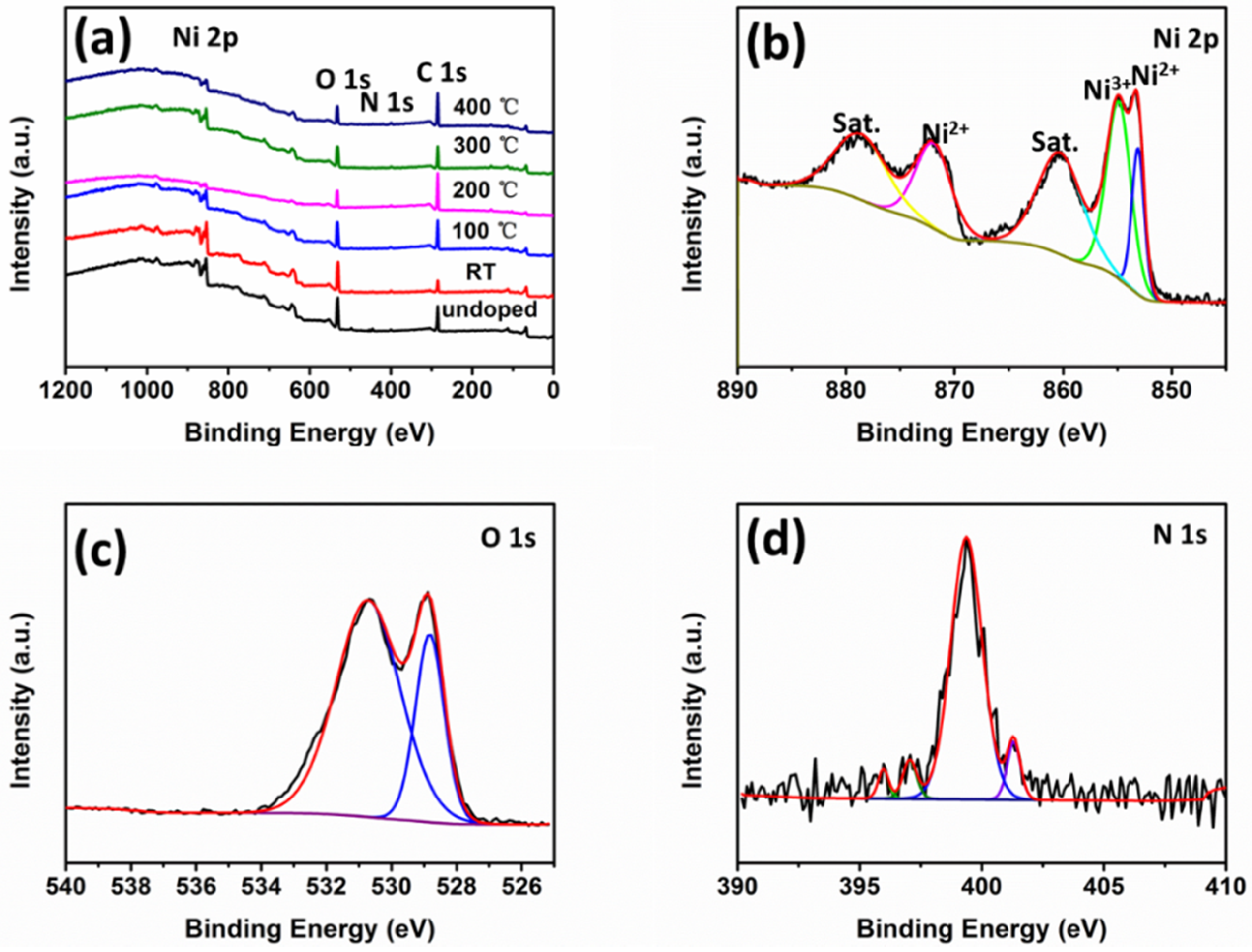
Figure 7.
(a) N 1s spectra of NiO thin films and (b) N content as a function of substrate temperature.
Figure 7.
(a) N 1s spectra of NiO thin films and (b) N content as a function of substrate temperature.

Figure 8.
(a) UV–Vis transmittance spectra and (b) optical bandgap energy of NiO thin films deposited at different substrate temperatures.
Figure 8.
(a) UV–Vis transmittance spectra and (b) optical bandgap energy of NiO thin films deposited at different substrate temperatures.

Figure 9.
(a) Mott–Schottky plots and (b) schematic energy band diagrams of NiO thin films deposited at different substrate temperatures.
Figure 9.
(a) Mott–Schottky plots and (b) schematic energy band diagrams of NiO thin films deposited at different substrate temperatures.
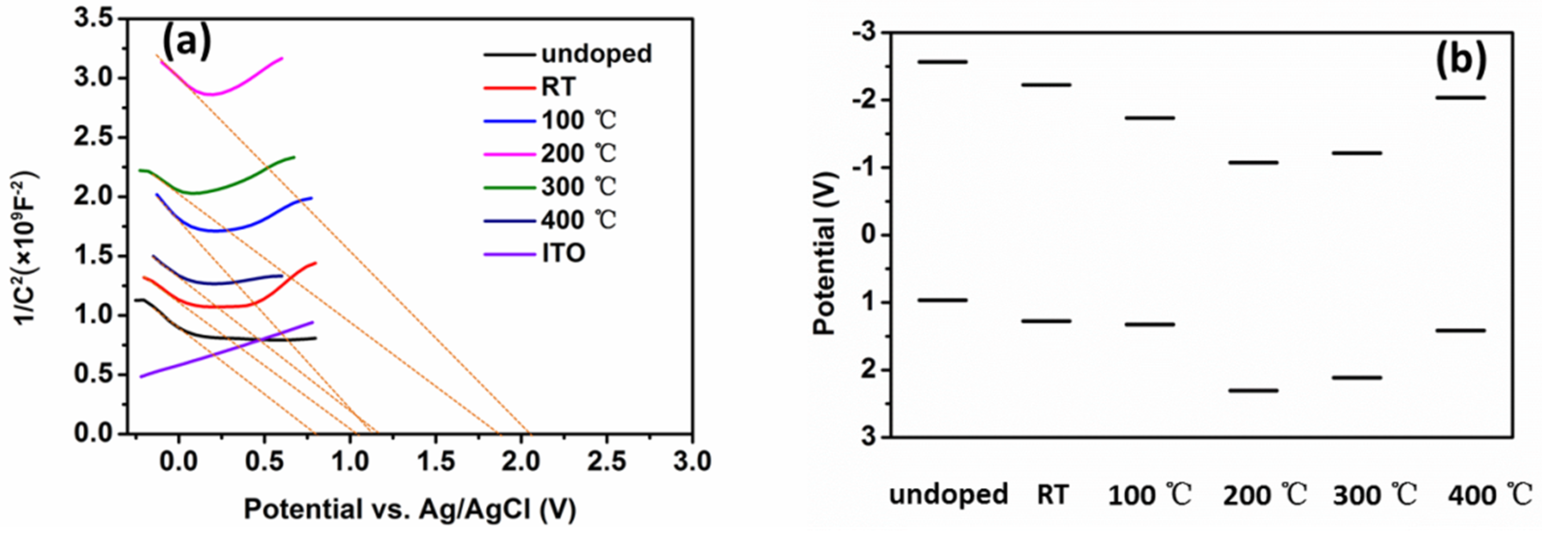
Figure 10.
Impedance of samples deposited at different substrate temperatures.

Figure 11.
Room-temperature photoluminescence (PL) spectra of NiO thin films deposited at different substrate temperatures.
Figure 11.
Room-temperature photoluminescence (PL) spectra of NiO thin films deposited at different substrate temperatures.


Table 1.
Deposition rate at different substrate temperature.
| Substrate Temperature (°C) | Deposition Rate (nm/min) |
|---|---|
| RT | 82 |
| 100 °C | 83 |
| 200 °C | 85 |
| 300 °C | 88 |
| 400 °C | 94 |
© 2019 by the authors. Licensee MDPI, Basel, Switzerland. This article is an open access article distributed under the terms and conditions of the Creative Commons Attribution (CC BY) license (http://creativecommons.org/licenses/by/4.0/).
Share and Cite
MDPI and ACS Style
Tian, Y.; Gong, L.; Qi, X.; Yang, Y.; Zhao, X. Effect of Substrate Temperature on the Optical and Electrical Properties of Nitrogen-Doped NiO Thin Films. Coatings 2019, 9, 634. https://doi.org/10.3390/coatings9100634
AMA Style
Tian Y, Gong L, Qi X, Yang Y, Zhao X. Effect of Substrate Temperature on the Optical and Electrical Properties of Nitrogen-Doped NiO Thin Films. Coatings. 2019; 9(10):634. https://doi.org/10.3390/coatings9100634
Chicago/Turabian StyleTian, Yuan, Lianguo Gong, Xueqian Qi, Yibiao Yang, and Xiaodan Zhao. 2019. "Effect of Substrate Temperature on the Optical and Electrical Properties of Nitrogen-Doped NiO Thin Films" Coatings 9, no. 10: 634. https://doi.org/10.3390/coatings9100634
Note that from the first issue of 2016, this journal uses article numbers instead of page numbers. See further details here.