Characterization of HfO2 Optical Coatings Deposited by MF Magnetron Sputtering


Faculty of Microsystem Electronics and Photonics, Wroclaw University of Science & Technology, Janiszewskiego 11/17, 50-372 Wroclaw, Poland
*
Author to whom correspondence should be addressed.
Coatings 2019, 9(2), 106; https://doi.org/10.3390/coatings9020106
Submission received: 12 December 2018
/
Revised: 1 February 2019
/
Accepted: 5 February 2019
/
Published: 8 February 2019
(This article belongs to the Special Issue Thin Film Deposition and Characterization Techniques)
Abstract
:The aim of this work is to determine the influence of medium frequency magnetron sputtering powers on the various properties of hafnium dioxide (HfO2) thin films. Microstructure observations show that an increase in the sputtering power has a significant influence on HfO2 films’ microstructure. As-deposited hafnia thin films exhibit nanocrystalline structure with a monoclinic phase, however the rise of the sputtering power results in an increase of crystallite sizes. Atomic force microscopy investigations show that the surface of the deposited films is smooth, crack-free, and composed of visible grains. The surface roughness and the value of the water contact angle increase with the increase of the sputtering power. Measurements of the optical properties show that HfO2 coatings are transparent in the visible wavelength range. A higher sputtering power causes a decrease of an average transmittance level and a simultaneous increase of the real part of the refractive index. Nanoindentation measurements reveal that the thin film hardness and Young’s elastic modulus increase with an increase in the sputtering power. Moreover, the results of plasticity index H/E and plastic resistance parameter H3/E2 are discussed. Based on the obtained results, a correlation between the sputtering power and the structural, surface, and optical properties, as well as the hardness and Young’s elastic modulus, were determined.
1. Introduction
In the last decade, hafnium dioxide (HfO2) has been widely studied because of its attractive properties and potential technological applications [1,2,3,4,5,6,7,8,9]. A high transmittance over a wide wavelength range, a hydrophobic nature, and hardness represent an important combination required in optical coatings [1,2,3,10,11]. HfO2 is a material with a high refractive index (1.85–2.1) [3,12] and a low absorption from ultraviolet to the mid-infrared [1,4,5]. Various optical applications of HfO2 thin films have been pursued such as, for example, chirped mirrors and band pass filters, UV mirrors with a high damage threshold, and heat mirrors for energy efficient windows. As a result of the high transparency, hafnia thin films can be used as antireflective coatings for night vision devices, IR optical devices, and in cameras used for space applications [3,4,5,6,13,14]. The band gap of HfO2 is ca. 5.7 eV, whereas the dielectric constant is 25 [4,10,11,12,15]. HfO2 is also considered to be one of the most promising candidates to replace SiO2 in Si-based gate electronic devices, because of their high dielectric constant and thermodynamic stability [1,16]. Moreover, there has been increased interest in the use of HfO2 as the insulator layer in the metal–insulator–metal (MIM) stack for RRAM (resistive random-access memory) applications [7,8]. Its hydrophobic nature along with its suitable optical properties open up new possibilities for the application of such coatings [3]. Only a few reports are available on the hydrophobic nature of HfO2 thin films. The value of the water contact angle for hafnia coatings in the literature varies from 80°–100° [17,18,19,20]. However, the properties of HfO2 films strongly depend on the preparation method and deposition conditions [2].
In the case of the transparent protective coatings used in everyday life, their mechanical and optical properties are crucial. Although many studies have been conducted on the microstructure, optical, and dielectric properties of HfO2 prepared under different growth conditions and thermal treatments, there are only a few reports regarding its mechanical behavior [12,13,21,22,23,24,25]. Vlček et al. [5] and Pi et al. [1] showed that the HfO2 thin films prepared by high-power impulse magnetron sputtering (HiPIMS) with a pulsed oxygen flow control had a relatively high refractive index of 2.07–2.12 at 550 nm. In the previous work [26] of Mazur et al., it was shown that the values of the refractive index at the same wavelength increased with the increase of the deposition power. Moreover, Vargas et al. [12] investigated the effect of the growth temperature on the optical properties of the HfO2 thin films deposited by magnetron sputtering. It was revealed that the band gap values of the films varied in the range of 5.78–6.17 eV, and the refractive index increased from 1.80 to 2.09 with the increase of the deposition temperature from 25–700 °C.
In this paper, the influence of medium frequency (MF) magnetron sputtering power on various properties of hafnia coatings are described. The microstructure properties of the deposited HfO2 thin films have already been reported in a rather short communication [26], while in the current paper, the discussion part was vastly extended and new results were reported. In this report, attention was focused on the effect of the sputtering power on the deposition rate, type of the crystalline growth, wettability, contact angle, roughness, and optical properties, which were not discussed previously. Moreover, the traditional and continuous stiffness nanoindentation techniques were compared, and the plasticity index as an indication of the wear resistance of deposited coatings was also evaluated. Furthermore, the obtained results for the prepared HfO2 thin films were compared to the literature data.
2. Materials and Methods
Pulsed magnetron sputtering can be achieved by applying an impulse (medium frequency (MF) or pulsed-DC (direct-current)) waveform of the electrical signal supplying the cathode of the magnetron, or an impulse dosing of the gas to the deposition chamber. A magnetron equipped with a high purity circular Hf target, with a diameter of 30 mm and thickness of 3 mm, was powered by the medium frequency (100 kHz, which corresponds to a single MF pulse duration of about 10 μs) 2 kW MSS type Dora Power System unipolar power supply, which is based on a resonant power stage. The power delivered to the magnetron was controlled by a microcontroller operated by self-developed software. It has to be emphasized that the discharge power was regulated by the pwm method [27,28], which is based on a ratio of the time–width of supplying an impulse to the whole duty cycle time. Therefore, the average power released to the target was dependent on the pwm coefficient. Using this method means that the amplitude of the discharge current (1.4 A) and voltage (1200 V) is the same in each pulse. In turn, the change of the sputtering power is not generated by the change of the discharge current or voltage, but by the variation of the number of impulses in the duty cycle time. In such way it was possible to obtain an average power of 200, 400, and 600 W, by applying a pwm coefficient of 35%, 70%, and 100%, respectively. The discharge current and voltage pulse shape does not change with the increase of the sputtering power, and therefore the kinetic energy of each negative oxygen ion should also remain the same. However, along with the rise of the average discharge power released to the magnetron, the number of pulses increased as a consequence of changing the pwm coefficient. This results in an increase in the total amount of the energy of the atoms and species bombarding the substrate. In such a case, the temperature of the substrate can raise and consequently improve the surface mobility. Thus, a more dense coating can be obtained. During the deposition process, substrates were not additionally heated or biased. The magnetron sputtering stand consisted of a rotary and diffusion pump system. The base pressure before the sputtering process was equal to 5 × 10⁻⁵ mbar. The HfO2 thin films were sputtered in a pure oxygen. The working pressure during each sputtering process was equal to 2 × 10⁻² mbar, and it was the lowest possible value for sustaining a continuous plasma discharge. The working pressure was controlled by the gas flow, applying a dynamic feedback (Beta-Erg company, Warsaw, Poland) to keep the pressure at a constant value through the entire sputtering process, which in each case lasted for 90 min. The distance between the target and substrate was set at 80 mm. The vacuum chamber had a cylindrical shape with a volume of roughly 9 dm3. The thickness of the HfO2 films deposited with 200, 400, and 600 W was measured using the Taylor Hobson CCI optical profiler (Taylor Hobson, Leicester, UK), and were equal to 370, 700, and 530 nm, respectively.
The structure of the films was determined by the X-ray diffraction (XRD) method, using a Siemens 5000 powder diffractometer (Siemens, Karlsruhe, Germany) with a Cu Kα X-ray (λ = 1.54056 Å). The correction for the broadening of the XRD instrument was taken into account, and the crystallite sizes were calculated using Scherrer’s equation [29]. A Tecnai G2 FEG Super-Twin transmission electron microscope (Thermo Fisher Scientific, Waltham, MA, USA) was used for the microstructure observations.
An atomic force microscope (UHV VT AFM/STM Omicron, Oxford Instruments, Abigdon, UK) working in the ultra-high vacuum conditions in a contact mode was used to measure surface topography and to analyse the roughness of the HfO2 thin films. The Attension Theta Lite optical tensiometer (Biolin Scientific, Gothenburg, Sweden) was used to evaluate the wettability of the prepared coatings. The contact angle was assessed using deionized water and ethylene glycol. Measurements were performed according to the sessile drop method [30]. The surface free energy was calculated using the Owens–Wendt (OWRK) geometric mean and Wu harmonic mean approach [31,32].
The optical properties were determined based on the transmission measurements carried out in the wavelength range of 350–1000 nm. The experimental system consisted of an Ocean Optics QE 65,000 spectrophotometer (Ocean Optics, Largo, FL, USA) and a coupled deuterium–halogen light source. The spectra were recorded using a light beam perpendicular to the sample. The refractive index and extinction coefficient were determined using the reverse engineering method employing the Cauchy model. Moreover, the Wemple-DiDomenico model was used to assess the optical properties of the deposited coatings [33,34].
The nanoindentation technique was used to determine the hardness and Young’s elastic modulus of the prepared thin films. These measurements were evaluated using a Keysight Nano Indenter G200 fitted (Needham, MA, USA) with a Berkovich indenter tip. The micro-mechanical properties of each film were evaluated using a traditional load-controlled test and continuous stiffness measurement (CSM), which is one of the significant improvements in nanoindentation testing [2,35,36,37]. The CSM technique is used for the measurements of the mechanical properties of thin films such as the contact stiffness, elastic modulus, hardness, creep resistance, and fatigue properties of the materials. The measurements can be made at exceedingly small penetration depths. Thus, the CSM technique is ideal for the measurement of the mechanical properties of thin films [35]. In the case of all of the samples, five traditional and CSM nanoindentation measurements were performed. For the determination of the hardness and Young’s elastic modulus from the load–displacement data, the Oliver and Pharr method was used [38].
3. Results and Discussion
3.1. Microstructure
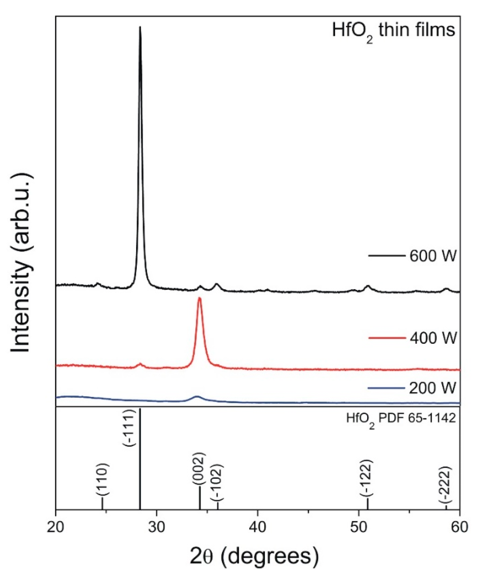
The structural properties of the prepared HfO2 thin films were analyzed using the XRD method. The diffraction patterns are shown in Figure 1 for the coatings deposited with various powers. It can be noticed that the peaks corresponding to the (−111) and (002) lattice planes appeared at 2θ angles equal to 28.3° and 34.3°, respectively. According to the powder diffraction file PDF (65-1142), all of the peaks’ positions of the HfO2 thin films correspond to the monoclinic phase [39]. The peak intensity of (−111) the crystal plane is the strongest for the film deposited at 600 W, which implies that it is textured among this plane, whereas the coatings deposited with lower powers were textured among the (002) crystal plane. It was found that with the increase of deposition power, the crystallite size of the prepared coatings was changed. The HfO2 thin films deposited at 200, 400, and 600 W were composed from crystallites with an average size of 6.5, 10.4, and 21.4 nm, respectively. Dave et al. [10] showed that the crystallite size for the HfO2 thin films with a monoclinic structure was in the range of 15–27 nm, and it increased simultaneously with the sputtering power. The enhancement in the crystallinity and crystal size of the hafnium oxide films can be associated with the change of the kinetic energy of the sputtered particles with the DC power. Dave et al. showed that as the sputtering power increased, the kinetic energy of the sputtered particles was also enhanced. Thus, the sputtered particles had sufficient energy to migrate on the substrate, resulting in the growth of the crystallite size. Moreover, in such a case, the overall crystallinity could be also improved. However, a further increase of the DC power supply over 50 W caused a degradation of the preferred crystal orientation and hindered the crystal growth of the deposited films [10]. This resulted in a lower intensity of a dominant peak and also caused a reduction of the crystallite size.
The position of the peaks visible in the diffraction spectra gives the macroscopic strain present in the thin film as a result of the residual stress. The XRD measurements of the as-deposited HfO2 thin films revealed a considerable shift of the diffraction peaks towards a lower 2θ angle. The type of out-of-plane macroscopic strain occurring in the measured coatings was determined on the basis of the Δd parameter from the following Equation [40]:
where d measured interplanar distance and dPDF measured the standard interplanar distance from [40].
In the case of the HfO2 thin films deposited with 200 and 400 W, the (002) plane was taken into account for the calculation, while for 600 W, it was the (−111) plane. The positive sign of the Δd parameter testified about the out-of-plane tensile macroscopic strain that occurred in the prepared coatings, which was increasing with an increase in the sputtering power.
One of the easiest and most convenient ways to determine the degree of the preferential orientation is the Lotgering method [41,42,43]. For the estimation of the texture factor, the following Equation was used:
where
ΣI(−111) denotes as the summation of the XRD peak intensities corresponding to the preferred orientation (in this case (−111)) and ΣI(hkl) is the summation of all of the peaks’ intensities that appear in the XRD pattern. In turn, ΣI0(−111) and ΣI0(hkl) are summations of the XRD peak intensities for a randomly oriented sample taken from the PDF cards. The Lotgering’s factor f = 0 corresponds to the sample with a completely random orientation, while f = 1 testifies about the perfect orientation for the calculated plane. In the case of the HfO2 thin films deposited with 600 W the preferred orientation was calculated for the (−111) lattice plane, while those sputtered with 200 and 400 W for (002) lattice plane. The Lotgering factor was calculated for a 2θ scan from 20° to 60°. The highest degree of orientation was determined for the HfO2 thin films deposited with 200 and 400 W, and it was in the range of 0.91 to 0.94. In turn, for the HfO2 thin films deposited with 600 W, the f factor was equal to 0.7. In the latter case, the Lotgering factor was smaller because of several visible peaks related to other lattice planes in the XRD pattern. The XRD measurement results are summarized in Table 1.
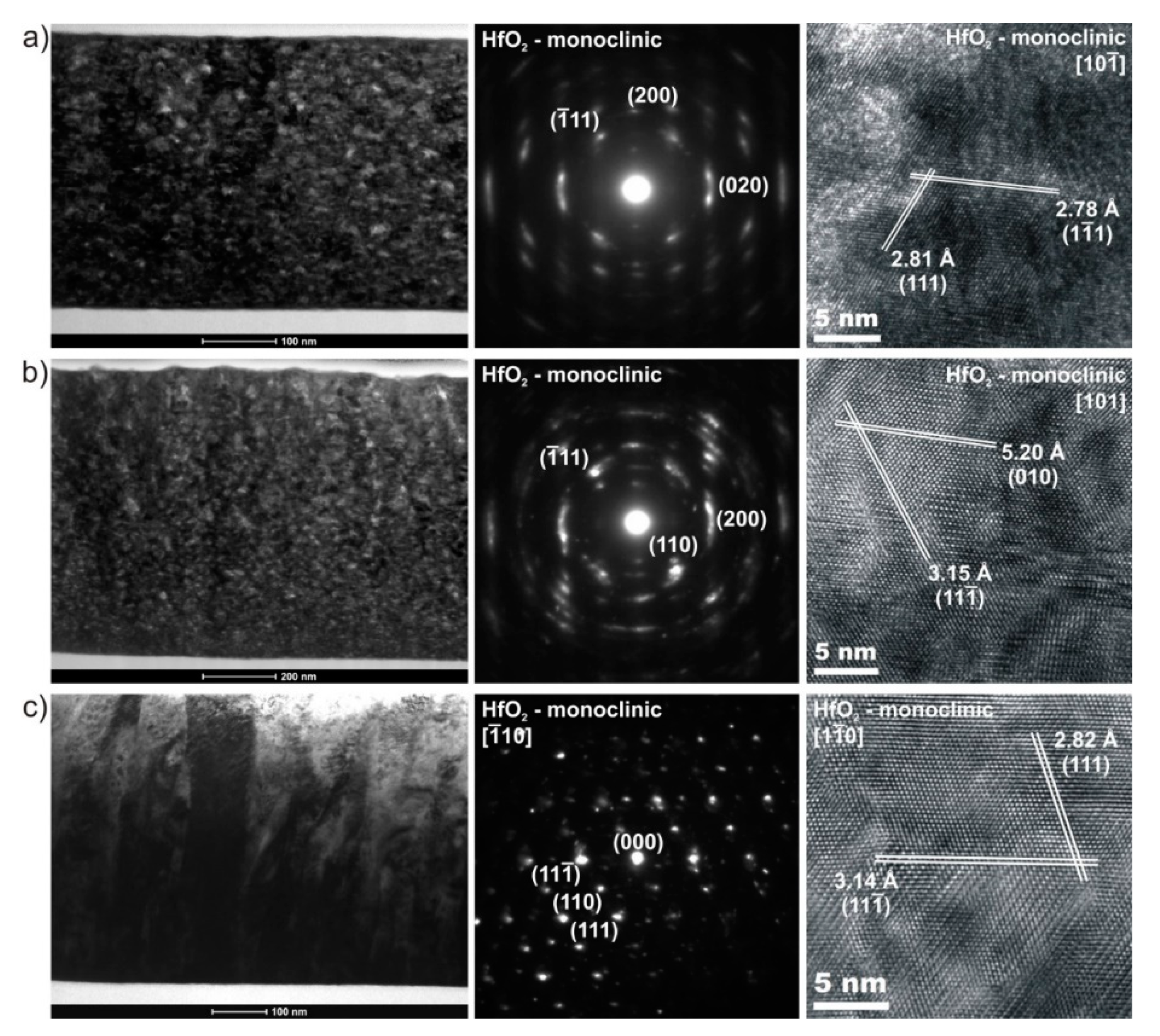
A detailed microstructure analysis was completed with the use of TEM analysis by means of bright field, selected area electron diffraction, and high-resolution imaging. The TEM bright field mode observations of the HfO2 coating prepared with a power of 200 W (Figure 2a) showed that the thin film had a fine-crystalline microstructure composed with voids of round shape with small diameter of 5–10 nm. An increase of the deposition power to 400 W caused an increase of the thickness of a sample, while the microstructure remained similar (Figure 2b). It had a nanocrystalline monoclinic HfO2 phase with small voids, however their amount was lower than in the case of the thin film deposited with 200 W. The sudden change of the microstructure to a coarse crystalline columnar one was observed for the thin film prepared with the highest power of 600 W (Figure 2c). The columns were rather defect-free, while their width was large, reaching even 100–120 nm, and the crystalline growth of the thin film started directly at the substrate. Those results can indicate that by supplying a magnetron with a higher deposition power, it is possible to sputter particles that reach the substrate with a lot higher kinetic energy. Thus, during the nucleation, a change of microstructure from fine-crystalline with visible voids, to a densely packed columnar one can be observed. The selected area electron diffraction (SAED) analysis of all of the samples showed, in each case, a strong texture, as their patterns had an almost spottish (Figure 2a,b) or spottish (Figure 2c) character. It is well known that the dislocation density, as well as the grain size, affect the shape of the spots in the selected area electron diffraction patterns. Spots visible in the patterns become more deformed from the usual, circular shape, to the irregular and stretched ones, because of the high accumulation of the dislocations. The dislocation can influence the crystal orientation causing the diffraction spots to be extended along the diffraction rings. Such dislocations may occur, for example, in the boundaries between the HfO2 crystallites (i.e., the smaller the size of the crystallites, the greater the number of dislocations). In the case of the presented SAED images, large and stretched diffraction spots could also be related to the small crystallites size and the fact that the selected area comprises multiple crystallites, which were not perfectly aligned along the same zone axis. In the case of the HfO2 thin film deposited with the highest power, the visible spots testify about occurrence of a highly crystalline microstructure. Moreover, the TEM images confirmed that this coating had a monoclinic phase, and that the growth direction was perpendicular to the (−111) plane. High resolution TEM studies confirmed that all of the samples were composed from a HfO2-monoclinic phase with various crystal planes of low indices.
The thickness of the deposited samples was equal to 370, 700, and 530 nm for the HfO2 films deposited with 200, 400, and 600 W of sputtering power, respectively. Taking into consideration those values, the target power density was in good correlation to the sputtering power and equal to 31.4, 62.7, and 94.1 W/cm2. As it can be noted, the thin films’ thickness does not increase linearly with the rise of deposition power. Moreover, the calculated deposition rate was equal to ca. 3.1, 5.8, and 4.4 nm·min−1 for the thin films deposited at 200, 400, and 600 W of sputtering power, respectively. In the case of 200 and 400 W, the sputtering power resulted in an almost double increase of the thin film thickness, while the microstructure of both coatings remained the same. It was fine crystalline with visible voids, and was similar to a kind of a spongy or blistery microstructure. However, a further increase of the sputtering power to 600 W resulted in a simultaneous decrease of thickness to 530 nm. This, in turn, can be related to the sudden change of the microstructure from the fine-crystalline with voids to the void-free and densely packed columnar one. In this case, the increase of the sputtering power, and, therefore, the rise of the total energy of the sputtered species resulted in the densification of the microstructure instead of the higher deposition rate of the coating. Such results indicate that in some cases, there might be no correlation between the sputtering power and the final thickness of the thin films, as there is also a significant influence of the microstructure evolution on this parameter.
3.2. Surface Properties
The surface morphology of the HfO2 films was studied using the AFM method, and the two-dimensional images of the surface obtained for the deposited coatings are shown in Figure 3. It can be observed that with the increase of the sputtering power, the maximum height of the surface profile increased several times, from 5.3 to 33.9 nm. In the case of the average surface height of the deposited coatings, the results showed a Gaussian-like symmetrical distribution in all of the samples, which can testify about the good homogeneity of the surface. The root mean square surface roughness (RMS) values increased gradually with the sputtering power. At the beginning of the thin film growth, the surface morphology reflects the morphology of the substrate. In the case of the thin films with a thickness exceeding several nanometers, the surface morphology is strongly influenced by their microstructure. As it was shown, the RMS value for the thin films deposited at 200 and 400 W increased only slightly from 1.33 to 1.96 nm. A further increase of the deposition power to 600 W resulted in a significant change of the microstructure, which caused the considerable rise of the RMS value up to 4.29 nm.
The wettability of the HfO2 coatings was evaluated by the measurements of the water contact angle using the sessile drop method at an ambient temperature. The first studies of the surface wettability were carried out by Young [44]. When a droplet of a liquid is placed on a flat surface, the balance of the three-phase interface is expressed by Young’s Equation (5), as follows:
where γl is the surface tension of liquid, γsl is the interfacial tension, γs is the surface free energy of a solid, and θ is the contact angle between the liquid–air interface and the surface [45].
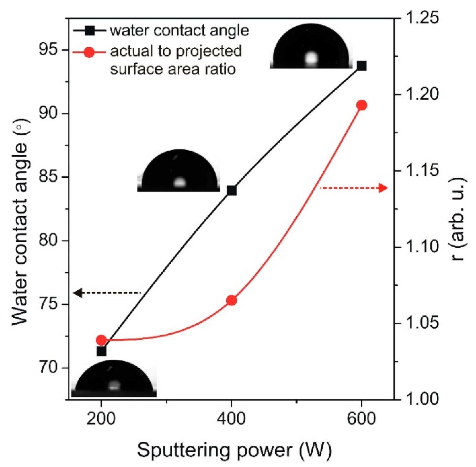
The value of the water contact angle for the as-deposited films increased with an increase of the sputtering power. The thin films deposited at 200 and 400 W were hydrophilic, and the values of the contact angle were equal to 71° and 84°, respectively. The HfO2 film deposited with a higher sputtering power (600 W) was hydrophobic and exhibited the highest value of a water contact angle, equal 94°. It has been already pointed out that the RMS surface roughness increased gradually with an increase of the deposition power from 1.33 to 4.29 nm. Therefore, apparently, the water contact angle is related to the surface topography. In fact, the contact angle and surface topography bear a linear relationship, which is related to the Wenzel model [46]. The Wenzel model was proposed half a century ago, and describes the contact angle on a real surface. This model considers the rough surface, but with a chemical homogeneity. The Wenzel model is expressed by the Equation (6), as follows:
where θ* is the apparent contact angle, θY is the equilibrium contact angle from Young’s Equation (5) on an ideal solid without any roughness, and r is the ratio of the actual area to the projected area of the surface.
According to the Wenzel model, it can be concluded that the surface roughness amplifies the wettability of the original surface [46,47]. The variation of the water contact angle and the actual-to-projected surface area ratio of the HfO2 thin films as a function of the sputtering power is presented in Figure 4. The estimation of the actual area of the thin films was performed using WSxM v.5.0 software [48] and AFM surface images. Because the thin films have some topography, the actual surface area is larger than the projected one, which, in the case of the presented paper, is equal to 1 × 1 µm2. In turn, the actual surface area was estimated by considering the surface as a collection of three-dimensional triangles, where each of them was formed by a point and its first neighbors. Then, the calculation of the actual area was done by simply adding them up. It can be noted that both the water contact angle and the ratio between the actual and projected area increased with an increase of the sputtering power of the HfO2 thin films.
Moreover, the analysis of the surface properties of the prepared thin films was completed by the measurements of the surface free energy, which is defined as the excess energy at the surface of the material, and is precisely related to the contact angle by Young’s equation. The geometric surface free energy is expressed by Owens and Wendt (OWRK) Equation (7), as follows:
where γli is the surface tension of a liquid; γs is the surface free energy of a solid, where d means dispersive and p polar component; and θ is the contact angle between the liquid–air interface and the surface [45].
Considering the data for the two liquids (i = 1, 2), a system of two equations is obtained.
Moreover, Wu also developed the harmonic mean method for two liquids, which can be expressed by Equation (8), as follows:
In the case of the performed studies, the analysis of the geometric (OWRK) and harmonic (Wu) surface free energy confirmed the contact angle measurement results (i.e., an increase of the contact angle value caused a decrease of the surface free energy). The contact angle, surface free energy, and root mean square surface roughness measurements’ results are summarized in Table 2.
3.3. Optical Properties
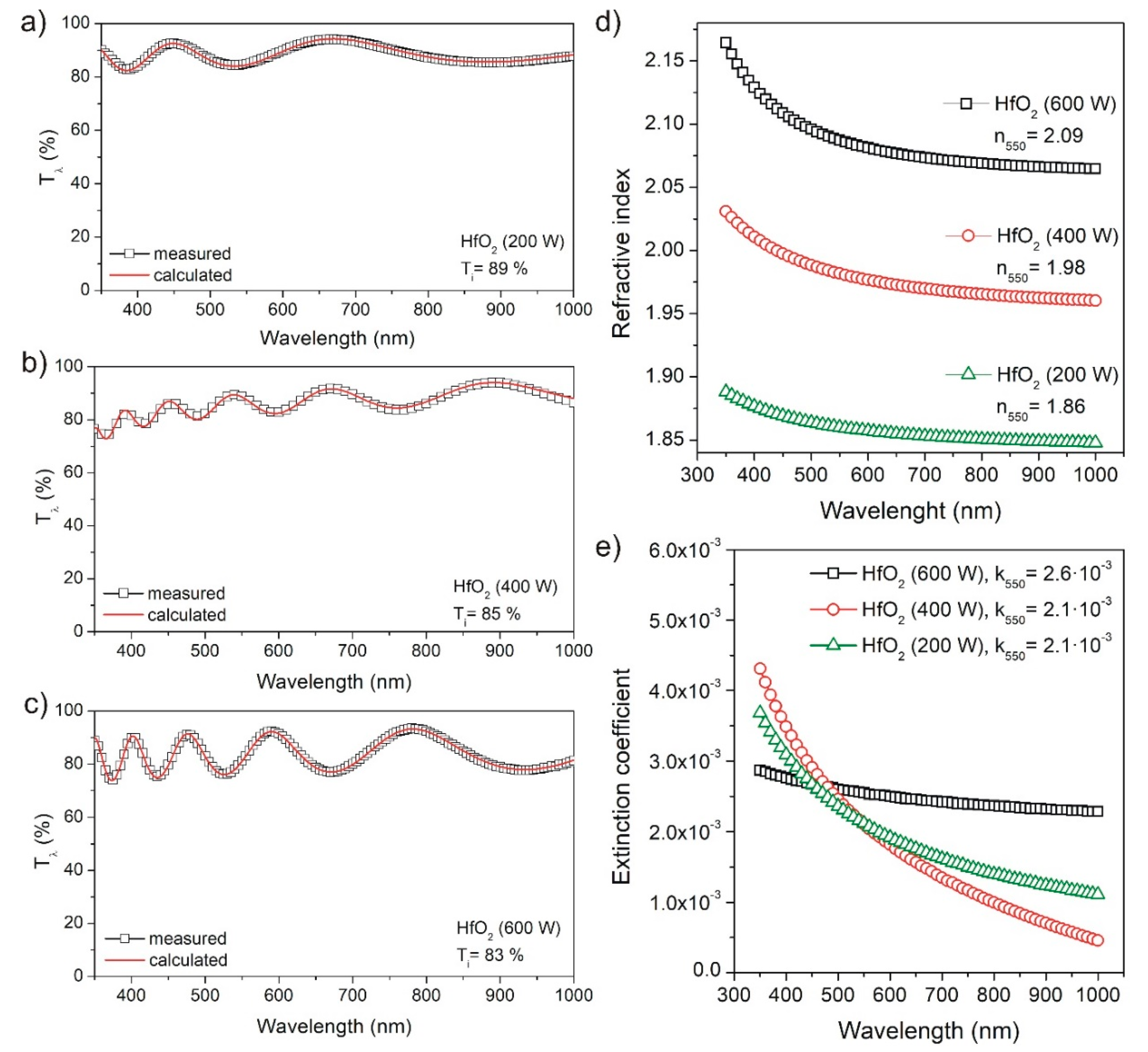
Figure 5 shows the measured transmission spectra of the HfO2 thin films deposited at different sputtering powers. The average transmission, Ti, was evaluated based on the transmission spectra in the function of the wavelength, using the envelope method originally developed by Manifacier et al. [49]. This technique consists of plotting two curves that pass through the maxima (Tλmax) and minima (Tλmin) of the actual transmission characteristic. In this paper, the average transmission was evaluated at the wavelength of 550 nm using Equation (9) [50], as follows:
In the case of some applications of optical coatings, it is highly desirable to obtain thin films with the highest possible transmission factor in the visible wavelength range. It was found that for the as-prepared hafnia coatings, their average transmission at 550 nm was approximately 80–90%, depending on the deposition power. The highest average transmission of 89% was exhibited for the coating deposited at 200 W. In the case of the two films deposited at the higher sputtering power of 400 and 600 W, a decrease of the transmittance level to 85% and 83%, respectively, was observed. Similar results were also reported by Dave et al. [10], where the transmittance level decreased with the increase of the deposition power. Moreover, the average transmission for the samples deposited at powers in the range of 30–60 W was found to be greater than 80% in the visible wavelength region. The surface roughness and transparency have an inverse relationship, as the first one provides the source of light scattering, which, in turn, decreases the transmission level of the films if the roughness is high enough [10]. However, in the case of the presented studies, the RMS surface roughness was at most 4.29 nm, which was too low of a value to have a direct, significant influence on the transparency level.
Moreover, except for the measured transmission spectra presented in Figure 5 (dotted measurement points), the corresponding modeled spectra (solid lines) were added for comparison. Using the reverse engineering method, the spectral characteristics of the refractive index (n) and extinction coefficient (k) were calculated and included in Figure 5d,e. The average transparency level can be affected by both the refractive index, which influences the amplitude of the maxima–minima interferences in the transmission spectrum, and the extinction coefficient, which has a direct effect on the absorption of the material. The extinction coefficient was equal to 2.1 × 10⁻³, 2.1 × 10⁻³, and 2.6 × 10⁻³ for the coatings deposited with 200, 400, and 600 W of sputtering power. Taking into account that in each case, the extinction coefficient was quite similar and its value was low, it can be assumed that the refractive index had a larger influence on Ti. In fact, the n value increased gradually from 1.86 to 2.09 for the films deposited with higher powers. It is known that the refractive index is dependent on the thin film density, which, according to the TEM results, is the highest for the HfO2 sputtered with 600 W. In this case, the microstructure is columnar and is densely packed with a low number of defects and dislocations. In turn, for the thin films deposited with lower powers, the microstructure consists of smaller crystallites with a higher number of defects. Furthermore, their microstructure also consists of a high number of voids with a round shape. Therefore, it is reasonable that with the increase of the sputtering power and significant change of microstructure, one could obtain HfO2 coatings with a higher refractive index.
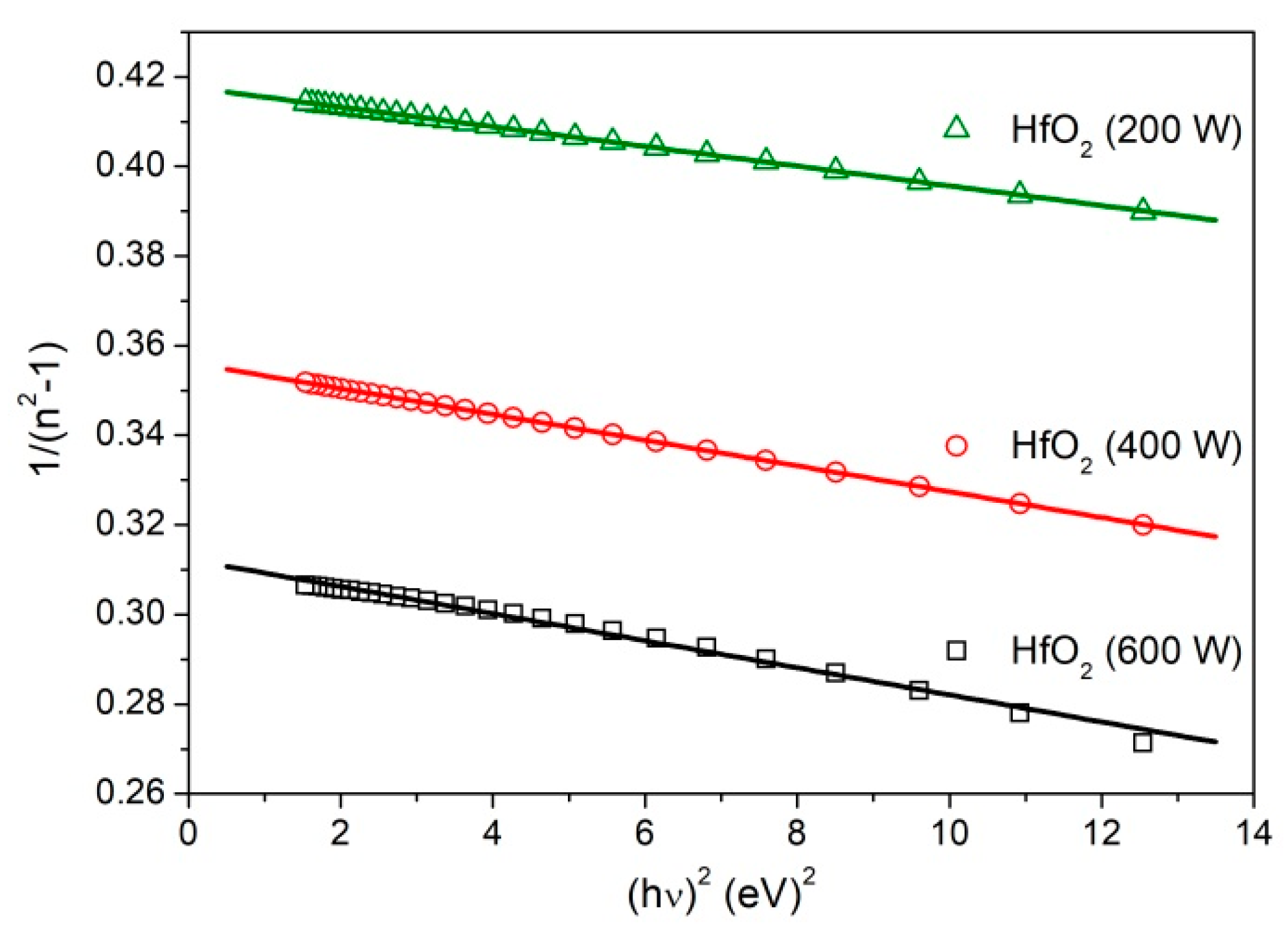
The refractive index can be fitted to an appropriate function such as the Wemple-DiDomenico model dispersion relationship [34]. The single-oscillator model of Equation (10) was used to fit the experimental data below the interband absorption edge, as follows:
where Eo is the single-oscillator energy and Ed is the dispersion energy or single-oscillator strength states for dispersion energy. Based on the Wemple and DiDomenico model [33,34], it is found that the dispersion energy (Ed) represents the strength of the interband optical transitions [33,34]. Ed is related to the structure, chemistry, and ionicity of the materials, and is independent on Eo. The dispersion parameters and the static dielectric constant (ε∞ = n2 at hν → 0) for the as-deposited HfO2 thin films can be calculated by plotting 1/(n2 − 1) against (hν)2, and fitting straight lines, as shown in Figure 6. The Eo and Ed values can be determined from the intercept of Eo/Ed and the slope of (EoEd)−1, respectively. The single-oscillator and dispersion energies derived from the linear parts of the plotted curves are Eo = 10.17 eV and Ed = 32.56 eV, and Eo = 11.12 eV and Ed = 31.22 eV for the HfO2 film deposited at 600 and 400 W of sputtering power, respectively. The dispersion parameters obtained for the film deposited at 200 W were equal to 13.78 and 32.99 eV for Eo and Ed, respectively. The static dielectric constant ε∞ decreased with a decrease of the sputtering power, and was equal to 4.202, 3.807, and 3.394. The dispersion parameters and ε∞ are summarized in Table 3.
Furthermore, the oscillator strength is given by f = EoEd [51]. The f-value for the as-deposited films decreased with an increase of the sputtering power from 454.55 to 331.13 (eV)2 for the films deposited at 200 and 600 W, respectively (Table 3). The long wavelength value of the refractive index (n∞) was also calculated by taking into account the approximation with a straight line and the linear parts of the curves plotted in Figure 6. The n∞ values increased with an increase of the sputtering power. As it was shown (Figure 6), the n∞ for films deposited at 200 and 400 W was equal to 1.842 and 1.951. The highest value of n∞ was obtained for HfO2 thin film deposited at 600 W sputtering power, and was equal 2.050 (Table 3).
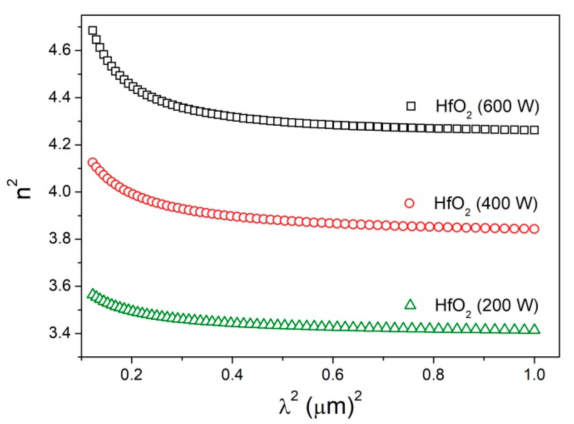
Moreover, the lattice dielectric constant εL was estimated with the use of the spectral dependence of n2 vs. λ2. The contributions of the free carriers and vibration modes to the dispersion were taken into account, which was described by the Drude model for the absorption of free charge carriers [52]. The dependence of the refractive index (n) on the lattice dielectric constant is as follows (11) [53]:
where N/m* is the ratio of the carrier concentration N to the effective mass m*, c is the speed of light, and e is the electronic charge. Figure 7 showed the plot of n2 versus λ2 calculated from Equation (11). The values of εL and N/m* were deduced from the extrapolation of these plots to λ2 = 0, and from the slope of the graph, respectively. The εL value for the as-deposited films increased with an increase of the sputtering power from 3.453 to 4.332 for the film deposited at 200 and 600 W, respectively. The ratio of the carrier concentration to the effective mass N/m* was equal to 8.3453 m−3 kg−1, 8.4453 m−3 kg−1, and 4.6053 m−3 kg−1 for HfO2 films deposited at 200, 400, and 600 W, respectively. The obtained values for εL and N/m* are presented in Table 3.
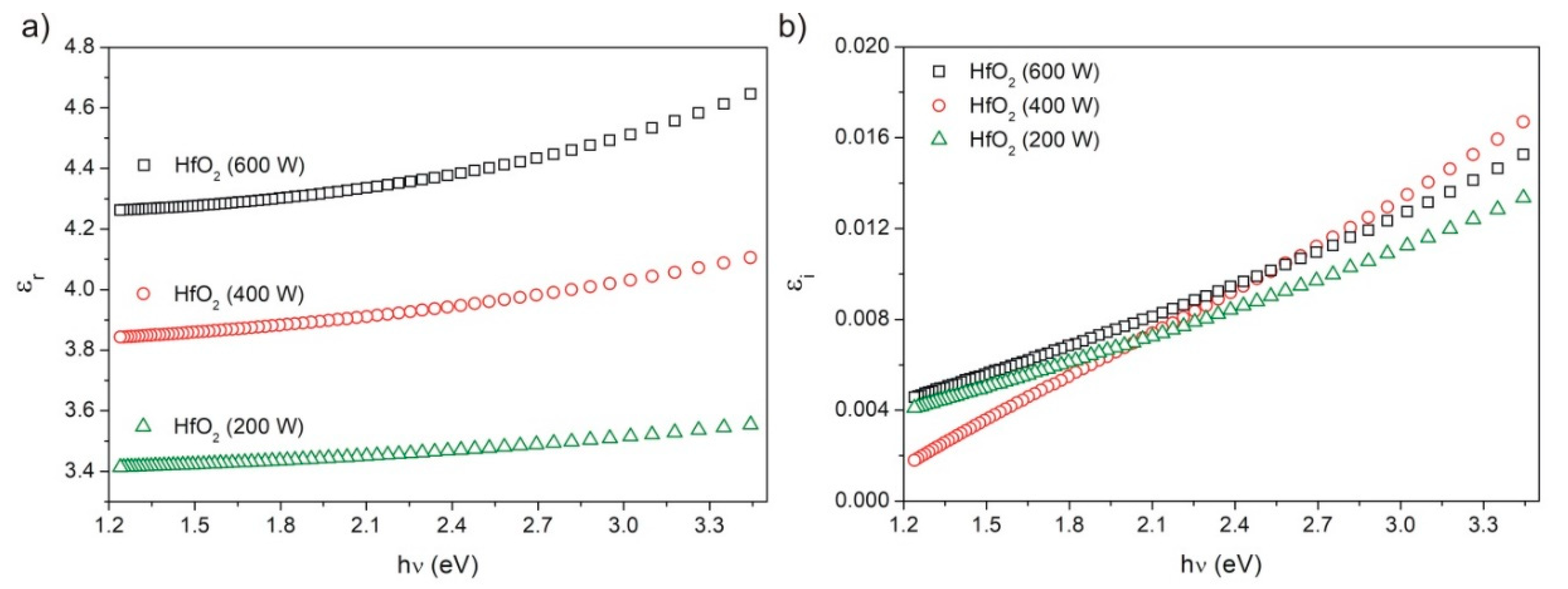
Taking into account the n(λ) and k(λ) spectra presented in Figure 5, the real εr and imaginary εi components of the electrical permittivity were also calculated. The complex electrical permittivity is defined as ε(ν) = εr + iεi. They are related to the n and k values, as follows: εr = n2 − k2 and εi = 2nk [54,55]. The spectra of εr and εi are presented in Figure 8a,b, respectively. It is clearly seen that both, the real and imaginary components of the relative permittivity decrease with an increase of the wavelength. Additionally, the low frequency permittivity was calculated, and it was equal to 3.36, 3.74, and 4.16 for the HfO2 thin films deposited with 200, 400, and 600 W of the sputtering power. Taking into account the obtained results, it can be assumed that an increase of the sputtering power influenced on the microstructure decreased the number of defects and voids, which in turn resulted in improving the dielectric properties of the deposited coatings.
3.4. Mechanical Properties
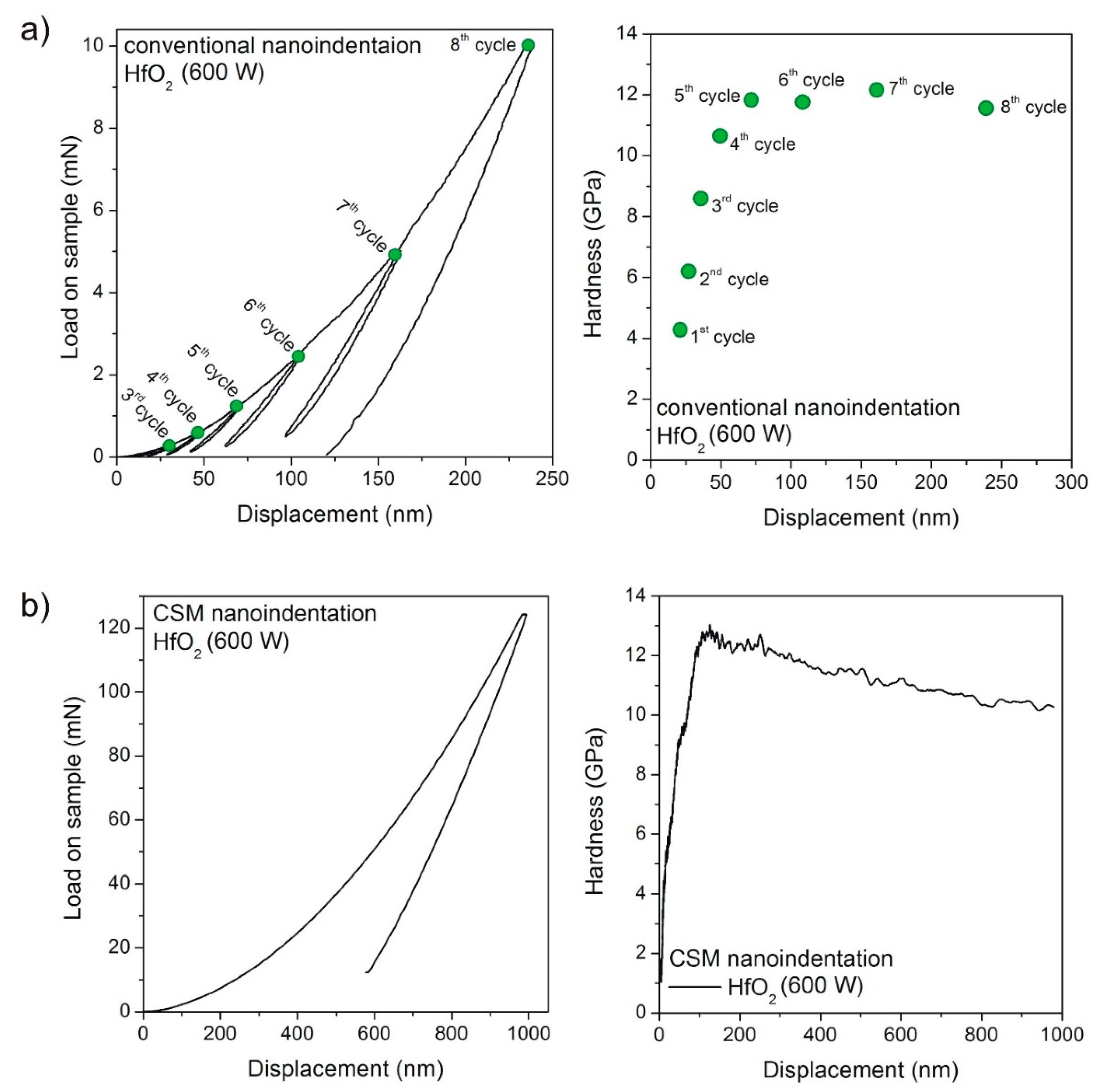
Nanoindentation measurements were performed to determine the mechanical properties, such as the hardness and elastic modulus of the HfO2 thin films. The simple comparison between the traditional testing and the CSM method is shown in Figure 9. The mechanical properties in the traditional testing are calculated from the depth of the penetrated material at the maximum indentation load of each loading cycle (Figure 9a), while in the CSM method, the hardness and elastic modulus can be obtained as a function of indentation depth [35] (Figure 9b).
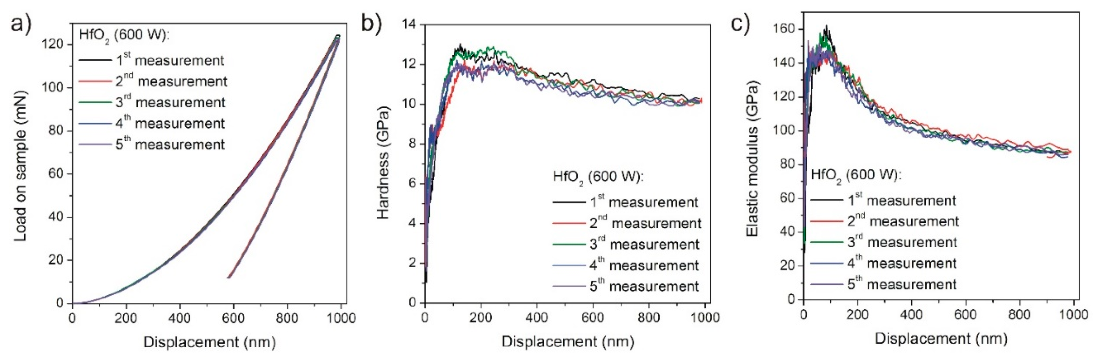
In our previous work [56], it was mentioned that unlike the quasi-static traditional indentation experiments, the CSM method is considered to be dynamic testing, which may matter in the case of time-dependent material behaviour. The CSM method gives the possibility to obtain mechanical properties (i.e., hardness and Young’s elastic modulus values) as a function of the indentation depth. This method allows for determining those values at very small depths, as the achievable resolution is much higher than in the case of the traditional load–unload nanoindentation testing. The thickness of each hafnia thin film did not exceed 1000 nm, therefore, this figure was used as the maximum depth. However, it is worth emphasizing that the values of the hardness and Young’s elastic modulus were extracted at a depth adequate to the thin film thickness, taking into consideration the 10% Buckle rule [57]. The results of the typical load–displacement curves for hte HfO2 films deposited at a 200, 400, and 600 W sputtering power are presented in Figure 10. Moreover, Figure 11a shows a comparison of the load–displacement curves obtained with the use of the CSM nanoindentation technique for HfO2 thin films deposited with 600 W of sputtering power. In turn, in Figure 11b,c, the values of the hardness and elastic modulus as a function of the HfO2 thin film depth were presented. Each nanoindentation measurement in both techniques was performed in a different place of the sample, and the only negligible differences were observed in the obtained curves, indicating a good homogeneity of the prepared HfO2 coatings over a large area.
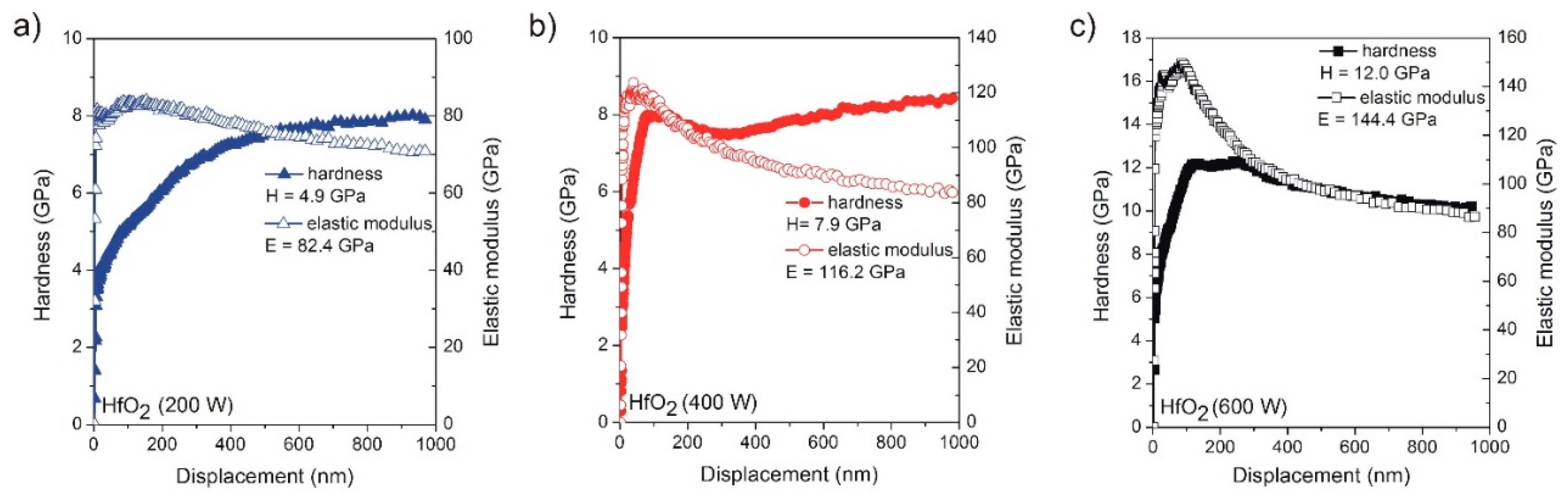
The results of the mean hardness–displacement and elastic modulus–displacement curves measured using the CSM method are presented in Figure 12. The HfO2 thin film deposited with a 200 W sputtering power exhibited the lowest hardness of ca. 4.9 GPa and an elastic modulus of 82.4 GPa. The further increase of the sputtering power to 400 and 600 W resulted in an increase of the hardness to ca. 7.9 and 12 GPa, respectively. The same growing tendency is observed for the values of the elastic modulus equal to up to ca. 116.2 and 144.4 GPa, obtained for the films deposited with 400 and 600 W power. Such a change of the mechanical properties of the deposited thin films can be directly attributed to the change of the microstructure. As it was shown in the TEM results, the sudden change of the microstructure from the fine-crystalline with voids, to the void-free and densely packed columnar one was observed for the films deposited with 600 W. Therefore, increasing the packing density of the deposited coatings also had an effect on the rise of the hardness and Young’s elastic modulus. According to the literature reports, the hardness of the HfO2 films is dependent on the type of deposition method. For example, Venkatachalam et al. [36] showed that the hardness of HfO2 thin film prepared by the radio frequency (RF) sputtering method was equal 8.4 GPa. In turn, Pi et al. [1] showed that the HfO2 thin films prepared by high-power impulse magnetron sputtering (HiPIMS) with a pulsed oxygen flow control had a hardness in the range of 13.4–17.6 GPa. Vlček et al. [5] also showed that the HfO2 coatings with a dominant monoclinic structure exhibited a hardness of 15–18 GPa. On the other hand, Tapily et al. [37] showed that the atomic layer deposition (ALD) method leads to the formation of HfO2 film with a hardness and elastic modulus equal 9.5 and 220 GPa, respectively. Moreover, Berdova et al. [58] showed that in the ALD method, there is a direct impact of the deposition temperature on the mechanical properties of the HfO2 thin films. The hardness and elastic modulus were slightly reduced in a function of the growing deposition temperature from 9.7 to 8.3 GPa, and 165 to 163 GPa, respectively [58].
Leyland and Matthews [59] proved that in the classical theory of wear, hardness is the primary material property that defines wear resistance. There is strong evidence to suggest that the elastic modulus can also have an important influence of wear behavior. The ratio between hardness (H) and elastic modulus (E) is defined as a plasticity index, which is widely quoted as a valuable measure for the determination of the limit of elastic behavior in a surface contact, which is clearly important in order to avoid wear [60]. Coatings characterized with high strength require a large value of the plasticity index H/E (i.e., large hardness combined with low modulus of elasticity). The results have shown that an increase in the sputtering power from 200 to 600 W, caused a gradual increase of the H/E parameter from 0.059 up to ca. 0.086 for the HfO2 thin films.
Another strong indicator that provides information on the resistance of materials to plastic deformation is H3/E2 [59,60,61]. This parameter shows that the contact loads needed to induce plasticity are higher in materials with larger values of H3/E2 (i.e., the likelihood of plastic deformation is reduced in materials with high hardness and low modulus, with H3/E2 being the controlling material parameter) [60,62,63]. The highest value of H3/E2 was equal to 0.083 for the HfO2 thin films deposited with 600 W. The results have shown that a decrease of the deposition power caused a gradual decrease of the plastic resistance parameter to ca. 0.037 and 0.017 for the HfO2 coatings deposited with 400 and 200 W, respectively.
4. Conclusions
In this paper, HfO2 thin films were deposited by MF magnetron sputtering with different powers of 200, 400, and 600 W, which had a significant effect on their structural, surface, optical, and tribological properties. In the case of the structural properties, XRD studies revealed that all of the deposited coatings had a nanocrystalline HfO2-monoclinic structure. An increase of the sputtering power, and simultaneously, the target power density, caused a considerable increase of the average crystallite size and a decrease of the dislocation density and lattice strain. The TEM investigations showed that the HfO2 thin films prepared with lower sputtering powers had a fine-crystalline structure with voids of a round shape, while the increase of the deposition energy resulted in a significant change in the microstructure, to a densely packed, columnar one. The surface of the prepared coatings was smooth, crack-free, and composed of visible grains. The analysis results of the root mean square surface roughness showed that it increased gradually with the sputtering power, from 1.33 to 4.29 nm. A similar tendency was observed for a water contact angle, which was directly related to the increase of a ratio between the actual and projected surface area, and was also confirmed by the Wenzel model. Moreover, all of the deposited coatings were well transparent in the visible wavelength range, with a transparency of approximately 80%–90%, depending on the deposition power. In the case of the optical constants, such as the refractive index and extinction coefficient, it was found that the first one increased with the increase of the sputtering power, while the latter remained similar for each coating. Nanoindentation measurements results showed that the hardness of the prepared thin films was in the range of 4.9 to 12.0 GPa.
It is worth emphasizing that the most beneficial coating, in terms of very good structural, surface, optical, and mechanical properties, was the HfO2 thin film deposited at 600 W of sputtering power. This coating had a densely packed microstructure without voids, therefore it also exhibited the highest hardness among the measured samples. Furthermore, the analysis of the mechanical properties revealed that the highest plasticity index H/E and plastic resistance H3/E2 was obtained for this coating. The HfO2 thin films deposited at 600 W had a smooth, hydrophobic surface and simultaneously exhibited a high transparency level, which are beneficial properties for its application in opto-electronic devices.
Author Contributions
Conceptualization, A.W., M.M., and D.K.; Methodology, A.W., M.M., and D.W.; Formal Analysis, A.W., A.O., M.M., D.K., and D.W.; Investigation, A.W., A.O., M.M., and D.W.; Visualization, A.W., A.O., and M.M.; Original Draft Preparation, A.W. and A.O.; Review and Editing, A.W. and A.O.; Supervision, D.K.; Funding Acquisition, D.K.
Funding
This work was co-financed from the sources given by the Polish National Science Centre (NCN) as a research project number DEC-2013/09/B/ST8/00140, and from statutory sources 0401/0130/18.
Conflicts of Interest
The authors declare no conflict of interest.
References
- Pi, N.W.; Zhang, M.; Jiang, J.; Belosludtsev, A.; Vlček, J.; Houška, J.; Meletis, E.I. Microstructure of hard and optically transparent HfO2 films prepared by high-power impulse magnetron sputtering with a pulsed oxygen flow control. Thin Solid Films 2017, 619, 239–249. [Google Scholar] [CrossRef]
- Fu, W.E.; He, B.C.; Chang, Y.Q. Surface mechanical property assessment of ultra-thin HfO2 films. Thin Solid Films 2013, 544, 212–217. [Google Scholar] [CrossRef]
- Jain, R.K.; Gautam, Y.K.; Dave, V.; Chawla, A.K.; Chandra, R. A study on structural, optical and hydrophobic properties of oblique angle sputter deposited HfO2 films. Appl. Surf. Sci. 2013, 283, 332–338. [Google Scholar] [CrossRef]
- Bright, T.J.; Watjen, J.I.; Zhang, Z.M.; Muratore, C.; Voevodin, A.A. Optical properties of HfO2 thin films deposited by magnetron sputtering: From the visible to the far-infrared. Thin Solid Films 2012, 520, 6793–6802. [Google Scholar] [CrossRef]
- Vlček, J.; Belosludtsev, A.; Rezek, J.; Houška, J.; Čapek, J.; Čerstvý, R.; Haviar, S. High-rate reactive high-power impulse magnetron sputtering of hard and optically transparent HfO2 films. Surf. Coat. Technol. 2016, 290, 58–64. [Google Scholar] [CrossRef]
- Al-Kuhaili, M.F. Optical properties of hafnium oxide thin films and their application in energy-efficient windows. Opt. Mater. 2004, 27, 383–387. [Google Scholar] [CrossRef]
- Walczyk, D.; Bertaud, T.; Sowinska, M.; Lukosius, M.; Schubert, M.A.; Fox, A.; Wolansky, D.; Scheit, A.; Fraschke, M.; Schoof, G.; et al. Resistive switching behavior in TiN/HfO2/Ti/TiN devices. In Proceedings of the 2012 International Semiconductor Conference Dresden-Grenoble (ISCDG), Grenoble, France, 24–26 September 2012; pp. 143–146. [Google Scholar]
- Sowinska, M.; Bertaud, T.; Walczyk, D.; Thiess, S.; Schubert, M.A.; Lukosius, M.; Drube, W.; Walczyk, Ch.; Schroeder, T. Hard X-ray photoelectron spectroscopy study of the electroforming in Ti/HfO2-based resistive switching structures. Appl. Phys. Lett. 2012, 100, 233509. [Google Scholar] [CrossRef]
- Schmeisser, D.; Kot, M.; Corrêa, S.A.; Das, C.; Henkel, K. Interface potentials, intrinsic defects, and passivation mechanisms in Al2O3, HfO2, and TiO2 ultrathin films. In Encyclopedia of Interfacial Chemistry: Surface Science and Electrochemistry; Elsevier: Oxford, UK, 2018; pp. 162–171. [Google Scholar]
- Dave, V.; Gupta, H.O.; Chandra, R. Nanostructured hydrophobic DC sputtered inorganic oxide coating for outdoor glass insulators. Appl. Surf. Sci. 2014, 295, 231–239. [Google Scholar] [CrossRef]
- Tan, T.; Liu, Z.; Li, Y. First-principles calculations of electronic and optical properties of Ti-doped monoclinic HfO2. J. Alloys Compd. 2012, 510, 78–82. [Google Scholar] [CrossRef]
- Vargas, M.; Murphy, N.R.; Ramana, C.V. Structure and optical properties of nanocrystalline hafnium oxide thin films. Opt. Mater. 2014, 37, 621–628. [Google Scholar] [CrossRef]
- Du, Q.; Wang, W.; Li, S.; Zhang, D.; Zheng, W. Effects of substrate temperature on the structural, optical and resistive switching properties of HfO2 films. Thin Solid Films 2016, 608, 21–25. [Google Scholar] [CrossRef]
- Franta, D.; Ohlídal, I.; Nečas, D.; Vižd’a, F.; Caha, O.; Hasoň, M.; Pokorný, P. Optical characterization of HfO2 thin films. Thin Solid Films 2011, 519, 6085–6091. [Google Scholar] [CrossRef]
- Pokhriyal, S.; Biswas, S. Doping dependent high-frequency dielectric properties of Hf1–xTixO2 nanoparticles. Mater. Today Proc. 2016, 3, 1311–1319. [Google Scholar] [CrossRef]
- Jin, P.; He, G.; Wang, P.H.; Liu, M.; Xiao, D.Q.; Gao, J.; Chen, H.S.; Chen, X.S.; Sun, Z.Q.; Zhang, M.; et al. Baking-temperature-modulated optical and electrical properties of HfTiOx gate dielectrics via sol-gel method. J. Alloys Compd. 2016, 688, 925–932. [Google Scholar] [CrossRef]
- Dave, V.; Dubey, P.; Gupta, H.O.; Chandra, R. Influence of sputtering pressure on the structural, optical and hydrophobic properties of sputtered deposited HfO2 coatings. Thin Solid Films 2013, 549, 2–7. [Google Scholar] [CrossRef]
- Linn, S.S.; Liao, C.S. The hydrophobicity and optical properties of the HfO2-deposited glass. Ceram. Int. 2013, 39, 353–358. [Google Scholar] [CrossRef]
- Linn, S.S.; Li, H.R. The optical properties of hydrophilic Hf-doped HfO2 nanoceramic films. Ceram. Int. 2013, 39, 7677–7683. [Google Scholar] [CrossRef]
- Nishide, T.; Honda, S.; Matsuura, M.; Idec, M. Surface, structural and optical properties of sol-gel derived HfO2 films. Thin Solid Films 2000, 371, 61–65. [Google Scholar] [CrossRef]
- Mazur, M.; Morgiel, J.; Wojcieszak, D.; Kaczmarek, D.; Kalisz, M. Effect of Nd doping on structure and improvement of the properties of TiO2 thin films. Surf. Coat. Technol. 2015, 270, 57–65. [Google Scholar] [CrossRef]
- Modreanu, M.; Sancho-Parramon, J.; Durand, O.; Servet, B.; Stchakovsky, M.; Eypert, C.; Naudin, C.; Knowles, A.; Bridou, F.; Ravet, M.F. Investigation of thermal annealing effects on microstructural and optical properties of HfO2 thin films. Appl. Surf. Sci. 2006, 253, 328–334. [Google Scholar] [CrossRef]
- Singh, V.; Sharma, S.K.; Kumar, D.; Nahar, R.K. Study of rapid thermal annealing on ultra-thin high-k HfO2 films properties for nanoscaled MOSFET technology. Microelectron. Eng. 2012, 91, 137–143. [Google Scholar] [CrossRef]
- Khairnar, A.G.; Mahajan, A.M. Effect of post-deposition annealing temperature on RF-sputtered HfO2 thin film for advanced CMOS technology. Solid State Sci. 2013, 15, 24–28. [Google Scholar] [CrossRef]
- Deng, B.; He, G.; Lv, J.G.; Chen, X.F.; Zhang, J.W.; Zhang, M.; Sun, Z.Q. Modulation of the structural and optical properties of sputtering-derived HfO2 films by deposition power. Opt. Mater. 2014, 37, 245–250. [Google Scholar] [CrossRef]
- Mazur, M.; Howind, T.; Gibson, D.; Kaczmarek, D.; Morgiel, J.; Wojcieszak, D.; Zhu, W.; Mazur, P. Modification of various properties of HfO2 thin films obtained by changing magnetron sputtering condition. Surf. Coat. Technol. 2017, 320, 426–431. [Google Scholar] [CrossRef]
- Wiatrowski, A.; Posadowski, W. The impact of medium frequency pulsed magnetron discharge power on the single probe Langmuir measurements and resulted plasma parameters. Mater. Sci. Pol. 2016, 34, 374–385. [Google Scholar] [CrossRef]
- Adamiak, B.; Wiatrowski, A.; Domaradzki, J.; Kaczmarek, D.; Wojcieszak, D.; Mazur, M. Preparation of multicomponent thin films by magnetron co-sputtering method: The Cu-Ti case study. Vacuum 2019, 161, 419–428. [Google Scholar] [CrossRef]
- Klug, H.P.; Alexander, L.E. X-ray Diffraction Procedures for Polycrystalline and Amorphous Materials; John Wiley and Sons: New York, NY, USA, 1974. [Google Scholar]
- Kwok, D.Y.; Neumann, A.W. Contact angle measurement and contact angle interpretation. Adv. Colloid Interface 1999, 81, 167–249. [Google Scholar] [CrossRef]
- Owens, D.K.; Wendt, R.C. Estimation of the surface free energy of polymers. J. Appl. Polym. Sci. 1969, 13, 1471–1747. [Google Scholar] [CrossRef]
- Della Volpe, C.; Maniglio, D.; Brugnara, M.; Siboni, S.; Morra, M. The solid surface free energy calculation I. In defence of the multicomponent approach. J. Colloid Interface Sci. 2004, 271, 434–453. [Google Scholar] [CrossRef]
- Wemple, S.H.; DiDomenico, J.M. Behavior of the electronic dielectric constant in covalent and ionic materials. Phys. Rev. B 1971, 3, 1338–1351. [Google Scholar] [CrossRef]
- Wemple, S.H. Refractive index of amorphous semiconductors and glasses. Phys. Rev. B 1973, 7, 3767–3777. [Google Scholar] [CrossRef]
- Li, X.; Bhushan, B. A review of nanoindentation continuous stiffness measurement technique and its applications. Mater. Charact. 2002, 48, 11–36. [Google Scholar] [CrossRef]
- Venkatachalam, D.K.; Bradby, J.E.; Saleh, M.N.; Ruffell, S.; Elliman, R.G. Nanomechanical properties of sputter-deposited HfO2 and HfxSi1-xO2 thin films. J. Appl. Phys. 2011, 110, 043527. [Google Scholar] [CrossRef]
- Tapily, K.; Jakes, J.E.; Stone, D.S.; Shrestha, P.; Gu, D.; Baumgart, H.; Elmustafa, A.A. Nanoindentation investigation of HfO2 and Al2O3 films grown by atomic layer deposition. J. Electrochem. Soc. 2008, 155, 545–551. [Google Scholar] [CrossRef]
- Oliver, W.C.; Pharr, G.M. An improved technique for determining hardness and elastic modulus using load and displacement sensing indentation experiments. J. Mater. Res. 1992, 7, 1564–1583. [Google Scholar] [CrossRef]
- Powder Diffraction File Card 65-1142; Joint Committee on Powder Diffraction Standards: Philadelphia, PA, USA, 2005.
- Domaradzki, J.; Kaczmarek, D.; Prociow, E.L.; Wojcieszak, D.; Sieradzka, K.; Mazur, M.; Lapinski, M. Study of structural and optical properties of TiO2:Tb thin films prepared by high energy reactive magnetron sputtering method. Opt. Appl. 2009, 39, 815–823. [Google Scholar]
- Lotgering, F.K. Topotactical reactions with ferromagnetic oxides having hexagonal crystal structures. J. Innorg. Nucl. Chem. 1959, 9, 113–123. [Google Scholar] [CrossRef]
- Brosnan, K.H.; Messing, G.L.; Meyer, R.J.; Vaudin, M.D. Texture measurements in <001> fiber-oriented PMN-PT. J. Am. Ceram. Soc. 2006, 89, 1965–1971. [Google Scholar] [CrossRef]
- Furuchima, R.; Tanaka, S.; Kato, Z.; Uematsu, K. Orientation distribution-Lotgering factor relationship in a polycrystalline material–as an example of bismuth titanate prepared by a magnetic field. J. Ceram. Soc. Jpn. 2010, 118, 921–926. [Google Scholar] [CrossRef]
- Young, T. An essay on the cohesion of fluids. Philos. Trans. R. Soc. Lond. 1805, 95, 65–87. [Google Scholar] [CrossRef]
- Hejda, F.; Solar, P.; Kousal, J. Surface free energy determination by contact angle measurements-a comparison of various approaches. In Proceedings of the WDS 2010, Prague, Czech Republic, 1–4 June 2010. [Google Scholar]
- Wenzel, R.N. Resistance of solid surfaces to wetting by water. Ind. Eng. Chem. 1936, 28, 988–994. [Google Scholar] [CrossRef]
- Seo, K.; Kim, M.; Kim, D.H. Re-derivation of Young’s equation, Wenzel equation, and Cassie-Baxter equation based on energy minimization. In Surface Energy; Intech: Rijeka, Croatia, 2015; pp. 1–22. [Google Scholar]
- Horcas, I.; Fernandez, R.; Gomez-Rodriguez, J.M.; Colchero, J.; Gomez-Herrero, J.; Baro, A.M. WSxM: A software for scanning probe microscopy and a tool for nanotechnology. Rev. Sci. Inst. 2007, 78, 013705. [Google Scholar] [CrossRef]
- Manifacier, J.C.; Gasiot, J.; Fillard, J.P. A simple method for the determination of the optical constants n, h and the thickness of a weakly absorbing thin film. J. Phys. E Sci. Inst. 1976, 9, 1002–1004. [Google Scholar] [CrossRef]
- Swanepoel, R. Determination of the thickness and optical constants of amorphous silicon. J. Phys. E Sci. Inst. 1983, 16, 1214–1222. [Google Scholar] [CrossRef]
- DiDomenico, M.; Wemple, S.H. Oxygen-octahedra ferroelectrics. I. Theory of electro-optical and nonlinear optical effects. J. Appl. Phys. 1969, 40, 720. [Google Scholar] [CrossRef]
- Khusayfan, N.M.; El-Nahass, M.M. Structural and optical characterizations of thin organic films of thioindigo. Ukr. J. Phys. Opt. 2016, 17, 10–20. [Google Scholar] [CrossRef]
- Kumar, G.A.; Thomas, J.; George, N.; Kumar, B.A.; Radhakrishnan, P.; Nampoori, V.P.N.; Vallabhan, C.P.G. Optical absorption studies of free (H2Pc) and rare earth (RePc) phthalocyanine doped borate glasses. Phys. Chem. Glasses 2000, 41, 89–93. [Google Scholar]
- Hodgson, J.N. Optical Absorption and Dispersion in Solids; Chapman and Hall: London, UK, 1970. [Google Scholar]
- Caglara, Y.; Ilican, S.; Caglar, M. Single-oscillator model and determination of optical constants of spray pyrolyzed amorphous SnO2 thin films. Eur. Phys. J. B 2007, 58, 251–256. [Google Scholar] [CrossRef]
- Mazur, M.; Howind, T.; Gibson, D.; Kaczmarek, D.; Song, S.; Wojcieszak, D.; Zhu, W.; Mazur, P.; Domaradzki, J.; Placido, F. Investigation of structural, optical and micro-mechanical properties of (NdyTi1−y)Ox thin films deposited by magnetron sputtering. Mater. Des. 2018, 85, 377–388. [Google Scholar] [CrossRef]
- Westbrook, J.H.; Conrad, H. The Science of Hardness Testing and Its Research Applications; American Society for Metals: Metals Park, OH, USA, 1973; pp. 453–491. [Google Scholar]
- Berdova, M.; Liu, X.; Wiemer, C.; Lamperti, A.; Tallarida, G.; Cianci, E.; Fanciulli, M.; Franssila, S. Hardness, elastic modulus, and wear resistance of hafnium oxide-based films grown by atomic layer deposition. J. Vac. Sci. Technol. A 2016, 34, 1–9. [Google Scholar] [CrossRef]
- Leyland, A.; Matthews, A. On the significance of the H/E ratio in wear control: A nanocomposite coating approach to optimized tribological behavior. Wear 2000, 246, 1–11. [Google Scholar] [CrossRef]
- Halling, J. Surface films in tribology. Tribologia 1982, 1, 15. [Google Scholar] [CrossRef]
- Chang, L.C.; Chang, C.Y.; Chen, Y.I. Mechanical properties and oxidation resistance of reactively sputtered Ta1–xZrxNy thin films. Surf. Coat. Technol. 2015, 280, 27–36. [Google Scholar] [CrossRef]
- Tsui, T.Y.; Pharr, G.M.; Oliver, W.C.; Bhatia, C.S.; White, R.L.; Anders, S.; Anders, A.; Brown, I.G. Nanoindentation and nanoscratching of hard carbon coatings for magnetic disks. Mater. Res. Soc. Symp. Proc. 1995, 383, 447–452. [Google Scholar] [CrossRef]
- Mazur, M.; Poniedziałek, A.; Kaczmarek, D.; Wojcieszak, D.; Domaradzki, J.; Gibson, D. Investigation of various properties of HfO2-TiO2 thin film composites deposited by multi-magnetron sputtering system. Appl. Surf. Sci. 2017, 421, 170–178. [Google Scholar] [CrossRef]
Figure 1.
XRD measurements results of the prepared hafnium dioxide (HfO2) thin films.

Figure 2.
TEM measurement results showing the bright field, selected area electron diffraction. and high-resolution images of the HfO2 thin films of the monoclinic phase deposited with a power of (a) 200, (b) 400, and (c) 600 W.
Figure 2.
TEM measurement results showing the bright field, selected area electron diffraction. and high-resolution images of the HfO2 thin films of the monoclinic phase deposited with a power of (a) 200, (b) 400, and (c) 600 W.

Figure 3.
Atomic force microscope (AFM) measurements results of the HfO2 thin films prepared by magnetron sputtering with various deposition powers of (a) 200, (b) 400, and (c) 600 W.
Figure 3.
Atomic force microscope (AFM) measurements results of the HfO2 thin films prepared by magnetron sputtering with various deposition powers of (a) 200, (b) 400, and (c) 600 W.
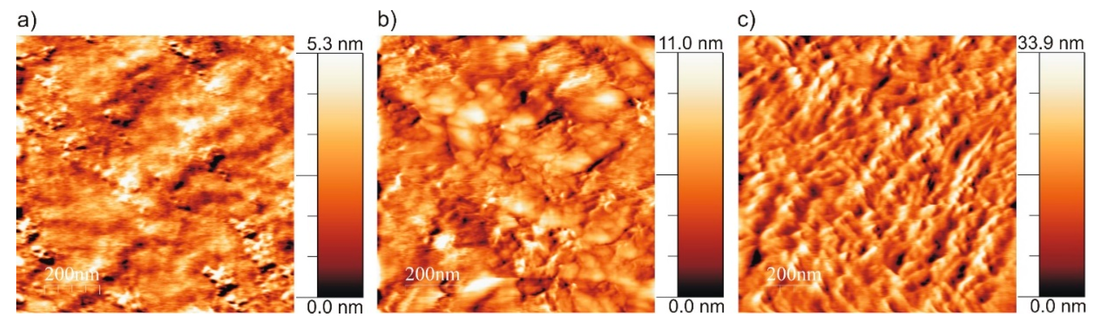
Figure 4.
Dependence of the water contact angle and r-values on the sputtering power.

Figure 5.
Comparison of transmission spectra (measured and modelled) of the HfO2 thin films deposited with various sputtering powers of (a) 200, (b) 400, and (c) 600 W, as well as the calculated (d) refractive index and (e) extinction coefficient.
Figure 5.
Comparison of transmission spectra (measured and modelled) of the HfO2 thin films deposited with various sputtering powers of (a) 200, (b) 400, and (c) 600 W, as well as the calculated (d) refractive index and (e) extinction coefficient.

Figure 6.
The 1/(n2 − 1) vs. (hν)2 plots for prepared HfO2 thin films.

Figure 7.
The n2 vs. λ2 plots for the prepared HfO2 thin films.

Figure 8.
Experimental dispersion characteristics of the (a) real and (b) imaginary parts of electronic dielectric constant for the prepared HfO2 thin films.
Figure 8.
Experimental dispersion characteristics of the (a) real and (b) imaginary parts of electronic dielectric constant for the prepared HfO2 thin films.

Figure 9.
Comparison of the traditional and continuous stiffness measurement (CSM) nanoindentation measurements: the (a) load–displacement curve and hardness from the traditional measurement, compared to the (b) load–displacement curve and hardness from the CSM measurement.
Figure 9.
Comparison of the traditional and continuous stiffness measurement (CSM) nanoindentation measurements: the (a) load–displacement curve and hardness from the traditional measurement, compared to the (b) load–displacement curve and hardness from the CSM measurement.

Figure 10.
Typical load–displacement curves of five measurements performed using traditional nanoindentation for HfO2 deposited at (a) 200, (b) 400, and (c) 600 W.
Figure 10.
Typical load–displacement curves of five measurements performed using traditional nanoindentation for HfO2 deposited at (a) 200, (b) 400, and (c) 600 W.
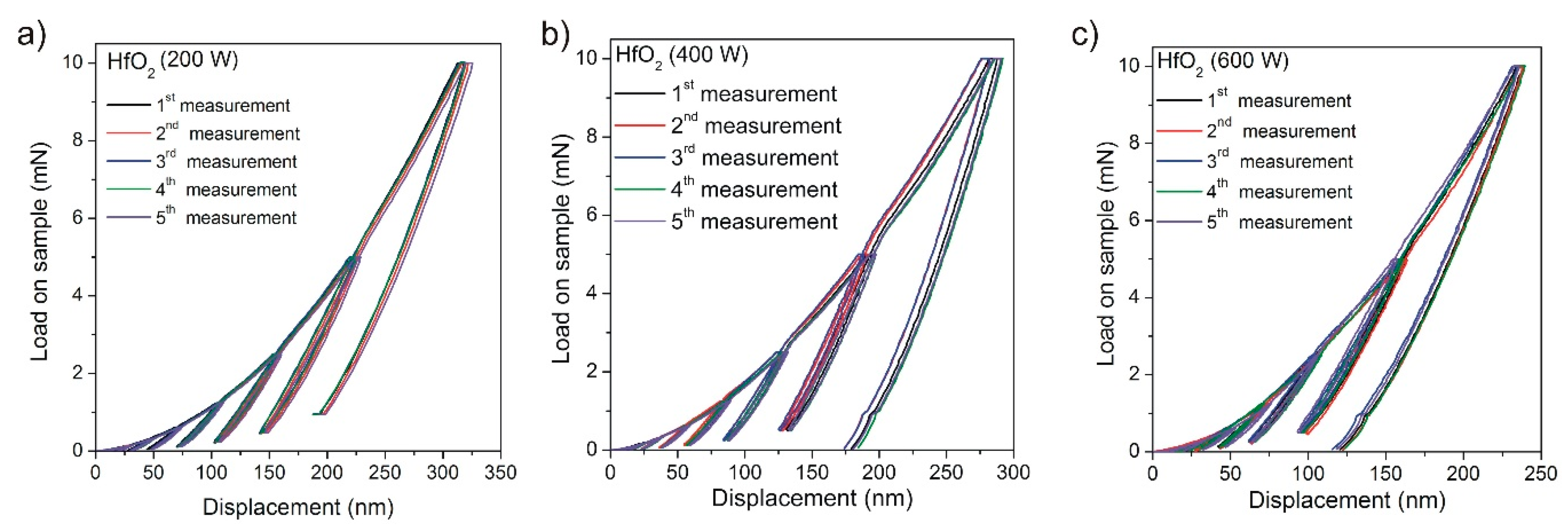
Figure 11.
Comparison of the five measurements performed using CSM nanoindentation: (a) load–displacement curves, (b) hardness, and (c) elastic modulus as a function of depth for the HfO2 thin films deposited at 600 W.
Figure 11.
Comparison of the five measurements performed using CSM nanoindentation: (a) load–displacement curves, (b) hardness, and (c) elastic modulus as a function of depth for the HfO2 thin films deposited at 600 W.

Figure 12.
Average values of hardness and Young’s elastic modulus for the thin films deposited with a sputtering power of (a) 200, (b) 400, and (c) 600 W.
Figure 12.
Average values of hardness and Young’s elastic modulus for the thin films deposited with a sputtering power of (a) 200, (b) 400, and (c) 600 W.

Table 1.
XRD measurements results for hafnium dioxide (HfO2) thin films prepared by magnetron sputtering with various sputtering powers.
Table 1.
XRD measurements results for hafnium dioxide (HfO2) thin films prepared by magnetron sputtering with various sputtering powers.
| Thin Film | Crystal Plane | D (nm) | d (nm) | Δd (%) | Type of Macroscopic Out-of-Plane Strain | f |
|---|---|---|---|---|---|---|
| PDF No. 65-1142 | (−111) | − | dpdf = 0.31453 | − | − | − |
| (002) | − | dpdf = 0.26146 | − | − | − | |
| HfO2 (600 W) | (−111) | 21.4 | 0.3146 | + 0.02 | tensile | 0.70 |
| HfO2 (400 W) | (002) | 10.4 | 0.2616 | + 0.05 | tensile | 0.91 |
| HfO2 (200 W) | (002) | 6.5 | 0.2638 | + 0.88 | tensile | 0.94 |
Designations: D—average crystallite size; d—interplanar distance; Δd—percentage change of interplanar distance as-compared to the standard (dPDF) one (PDF no. 65-1142); f—degree of preferential orientation.
Table 2.
Results of the surface free energy investigations of the prepared HfO2 thin films.
| Thin Film | Surface Free Energy (mN/m) | Water Contact Angle (°) | Ethylene Glycol Contact Angle (°) | r | |||||
|---|---|---|---|---|---|---|---|---|---|
| Geometric | Harmonic | ||||||||
| d | p | t | d | p | t | ||||
| HfO2 (200 W) | 9.8 | 22.8 | 32.6 | 22.8 | 13.7 | 36.5 | 71 | 48 | 1.039 |
| HfO2 (400 W) | 12.9 | 10.6 | 23.5 | 15.4 | 12.5 | 27.9 | 84 | 68 | 1.065 |
| HfO2 (600 W) | 17.5 | 4.3 | 21.8 | 14.5 | 10.0 | 24.5 | 94 | 69 | 1.193 |
Designations:d—dispersive component; p—polar component; t—total value of surface free energy; r—actual to projected surface area ratio.
Table 3.
Influence of the sputtering power on the optical parameters of the prepared HfO2 thin films.
Table 3.
Influence of the sputtering power on the optical parameters of the prepared HfO2 thin films.
| Thin Film | Eo (eV) | Ed (eV) | f (eV)2 | n∞ | ε∞ | εL | N/m* (m−3 kg−1) |
|---|---|---|---|---|---|---|---|
| HfO2 (200 W) | 13.78 | 32.99 | 454.55 | 1.842 | 3.394 | 3.453 | 4.6053 |
| HfO2 (400 W) | 11.12 | 31.22 | 347.22 | 1.951 | 3.807 | 3.915 | 8.4453 |
| HfO2 (600 W) | 10.17 | 32.56 | 331.13 | 2.050 | 4.202 | 4.332 | 8.3453 |
Designations: Eo—single-oscillator energy; Ed—dispersion energy; f—oscillator strength; n∞—long wavelength value of the refractive index; ε∞—static dielectric constant; εL—lattice dielectric constant; N/m*—ratio of the carrier concentration to the effective mass.
© 2019 by the authors. Licensee MDPI, Basel, Switzerland. This article is an open access article distributed under the terms and conditions of the Creative Commons Attribution (CC BY) license (http://creativecommons.org/licenses/by/4.0/).
Share and Cite
MDPI and ACS Style
Wiatrowski, A.; Obstarczyk, A.; Mazur, M.; Kaczmarek, D.; Wojcieszak, D. Characterization of HfO2 Optical Coatings Deposited by MF Magnetron Sputtering. Coatings 2019, 9, 106. https://doi.org/10.3390/coatings9020106
AMA Style
Wiatrowski A, Obstarczyk A, Mazur M, Kaczmarek D, Wojcieszak D. Characterization of HfO2 Optical Coatings Deposited by MF Magnetron Sputtering. Coatings. 2019; 9(2):106. https://doi.org/10.3390/coatings9020106
Chicago/Turabian StyleWiatrowski, Artur, Agata Obstarczyk, Michał Mazur, Danuta Kaczmarek, and Damian Wojcieszak. 2019. "Characterization of HfO2 Optical Coatings Deposited by MF Magnetron Sputtering" Coatings 9, no. 2: 106. https://doi.org/10.3390/coatings9020106
Note that from the first issue of 2016, this journal uses article numbers instead of page numbers. See further details here.