Article

Self-Ordered Orientation of Crystalline Hexagonal Boron Nitride Nanodomains Embedded in Boron Carbonitride Films for Band Gap Engineering

State Key Laboratory of Superhard Materials, College of Physics, Jilin University, No. 2699 Qianjin Street, Changchun 130012, China
*
Author to whom correspondence should be addressed.
Coatings 2019, 9(3), 185; https://doi.org/10.3390/coatings9030185
Submission received: 17 February 2019 / Revised: 4 March 2019 / Accepted: 6 March 2019 / Published: 12 March 2019
(This article belongs to the Special Issue Advanced Thin Films Deposited by Magnetron Sputtering)

Abstract

:
Boron carbonitride (BCN) films containing hybridized bonds involving elements B, C, and N over wide compositional ranges enable an abundant variety of new materials, electronic structures, properties, and applications, owing to their semiconducting properties with variable band gaps. However, it still remains challenging to achieve band gap-engineered BCN ternary with a controllable composition and well-established ordered structure. Herein, we report on the synthesis and characterization of hybridized BCN materials, consisting of self-ordered hexagonal BN (h-BN) crystalline nanodomains, with its aligned basal planes preferentially perpendicular to the substrate, depending on the growth conditions. The observation of the two sets of different band absorptions suggests that the h-BN nanodomains are distinguished enough to resume their individual band gap identity from the BCN films, which decreases as the carbon content increases in the BCN matrix, due to the doping and/or boundary effect. Our results reveal that the structural features and band gap of this form of hybrid BCN films are strongly correlated with the kinetic growth factors, making it a great system for further fundamental physical research and for potential in the development of band gap-engineered applications in optoelectronics.

Graphical Abstract

1. Introduction

The atomic bonding similarity amongst boron (B), carbon (C), and nitrogen (N) allows for the formation of a ternary boron carbonitride (BCN) system with a wide compositional range, including typical materials, such as diamond, graphite, fullerene, cubic BN (c-BN), hexagonal BN (h-BN), B4C, C3N4, BCN, BC2N, and so on [1,2,3], consequently, when combining their properties, making them adaptable for diverse applications [4,5,6]. Particularly, hybridizing between semi-metallic graphite and insulating BN [7], BCN ternary exhibits excellent semiconducting properties with an adjustable band gap, hence making it a suitable candidate in optoelectronic devices, luminescent devices, transistors, and micro-electrical-mechanical system (MEMS), just to name a few [8,9,10,11,12].
Recent studies on the optical and electronic properties of the BCN system have indicated that the band gaps of BCN compounds are determined not only by the elemental constitution, but also by other structural properties. For instance, the optical band gap value differs from 1.48 to 3.64 eV for BCN films with the same stoichiometry [13,14,15]. The band gap value of the BC2N films was found to depend on the measurement method [16]. Moreover, a band gap of BCN nanosheets can be opened or shrunk by hybridizing the h-BN domains in a graphene matrix [17], or the graphene domains in a h-BN planar matrix [18]. This may contradict the theoretical predictions in which the band gap of BCN would decrease monotonically with increasing carbon content [19,20,21]. Instead, it further suggests that besides the elemental composition, the structural properties, such as compositional order/disorder, may play alternative important roles in band gap-tuning.
So far, the BCN films have been synthesized by various techniques, including magnetron sputtering [22], pulsed laser deposition [23], chemical vapor deposition [24,25,26], ion beam deposition [27], and so on [7,28,29,30]. However, BCN films have not found the attention they deserve, which mostly has to do with the preparation problems of achieving a controllable composition and well-established ordered structure by simply changing the growth kinetics. This is usually correlated to the fact that elemental and/or binary phase segregation would occur instead of forming a uniform BCN network [16,31,32]. During the growth process, B, C, and N atoms prefer to combine differently as a result of their chemical properties, for example, B and C can exist both as elements and as part of compounds, while N could exist in the films only as compound [27,33,34,35]. Indeed, taking the advantage of the immiscibility between BN and graphite [23,36], the layer by layer composite structure of h-BN and graphene, planar BCN nanosheets consisting of h-BN domains, and h-BN nanosheets containing graphene quantum dots have been synthesized successfully, and have demonstrated the superior capability of manipulating their band gap [17,37,38,39]. This actually stimulates alternative thoughts to control the band gaps of the BCN films via both the elemental compositions and structural features, in which the well-defined evolution of the structural features and the precise intermixing of B, C and N with regards to the deposition process, are a high prerequisite.
Therefore, it is the aim of this work to elucidate the correlation of the optical band gap with the elemental composition and the structural features, by systematic studies of the characteristics of BCN films with specific structures and their corresponding growth kinetics. Herein, we report the synthesis and characterization of hybridized BCN films consisting of self-ordered crystalline h-BN nanodomains by means of a radio frequency (r.f.) magnetron sputtering method, which ensures a uniform elemental composition and conformal deposition over a large area. The as-obtained h-BN crystalline nanodomains orient with its planar basal planes preferentially perpendicular to the substrate, depending on the growth conditions that are homogeneously distributed within the BCN films. The optical results of the oriented BCN films exhibit two sets of distinct band absorption values as a result of the h-BN nanodomains and BCN matrix, respectively. The highly oriented h-BN nanodomains separated by a BCN matrix retain their distinct optical band gap identities, decreasing as the carbon content increases, as a result of the doping and/or boundary effect. This form of BCN film with separated oriented h-BN crystalline nanodomains and a wide range of compositions exhibits adjustable optical band gaps, therefore making it a promising system for fundamental physical investigations and potential optoelectronic applications with band gap, which can be easily tuned during a film deposition.

2. Materials and Methods

2.1. Film Deposition

All of the BCN films were deposited on a (100)-oriented silicon (Si) substrate by the r.f. (13.56 MHz) magnetron sputtering of a h-BN target (60 mm in diameter) with a graphite ring (60 and 68 mm in inner and external diameter, respectively) in either an argon (Ar) gas or a gas mix of nitrogen (N2) and Ar with different N2/Ar flow ratios. Prior to deposition, the Si substrates were ultrasonically cleaned in acetone, alcohol, and deionized water, and then blow-dried with nitrogen gas. The substrate holder was located directly above the target. The distance between the target and the substrate was kept at 80 mm during the deposition. The base pressure of the deposition chamber was below 3 × 10⁻⁵ Pa, and the working pressure was approximately 2 Pa. The sputtering power of the target was set at 150 W. The target was sputter-cleaned for 2 min before each deposition. During the deposition, the substrate holder was rotated uniformly in order to reduce the inhomogeneity in the film quality and composition.

2.2. Film Characterization

For all of the synthesized BCN films, the X-ray diffraction (XRD, D/MAX-2400, Rigaku, Tokyo, Japan) patterns show no distinct peak, except for the characteristic peak of monocrystalline silicon, revealing that they are amorphous. The bond structure and composition of the films were analyzed by Fourier transform infrared spectroscopy (FTIR, Vertex 80 V, Bruker, Karlsruhe, Germany) in reflection mode. The chemical composition and bonding states were investigated using X-ray photoelectron spectroscopy (XPS, ESCALAB 250, Thermo Fisher Scientific, Waltham, MA, USA) operating with Al-Kα radiation (hν = 1486.6 eV) and detecting a chamber pressure of 2.6 × 10⁻⁹ mbar). The micro-Raman spectrometer (LabRAM HR Evolution, HORIBA Scientific, Paris, France) was used to elucidate the chemical bonding state of the as-synthesized BCN films. The microtopography and microstructures of these samples were detected using a high-resolution scanning electron microscope (SEM, Magellan 400, FEI, Hillsboro, OR, USA) and transmission electron microscope (TEM, JEM-2200FS, JEOL, Tokyo, Japan). The TEM cross-section was obtained using a focused ion beam (FIB) after the deposition of the platinum bars. The ultraviolet-visible (UV-Vis) light absorbance of the films was measured using a LKB Ultraspec III UV-vis spectrophotometer (UV-3150, SHIMADZU, Kyoto, Japan), for wavelengths ranging from 1000 to 200 nm, with reference to that of an uncoated substrate. The optical band gap was then determined by fitting the absorption data to the Tauc relation.

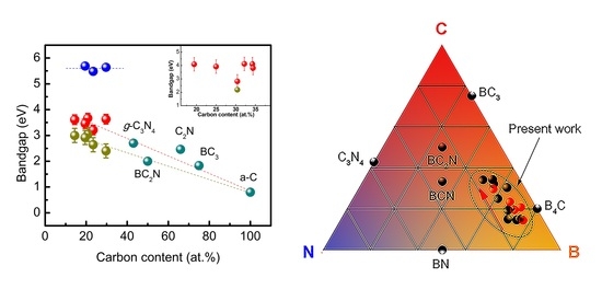
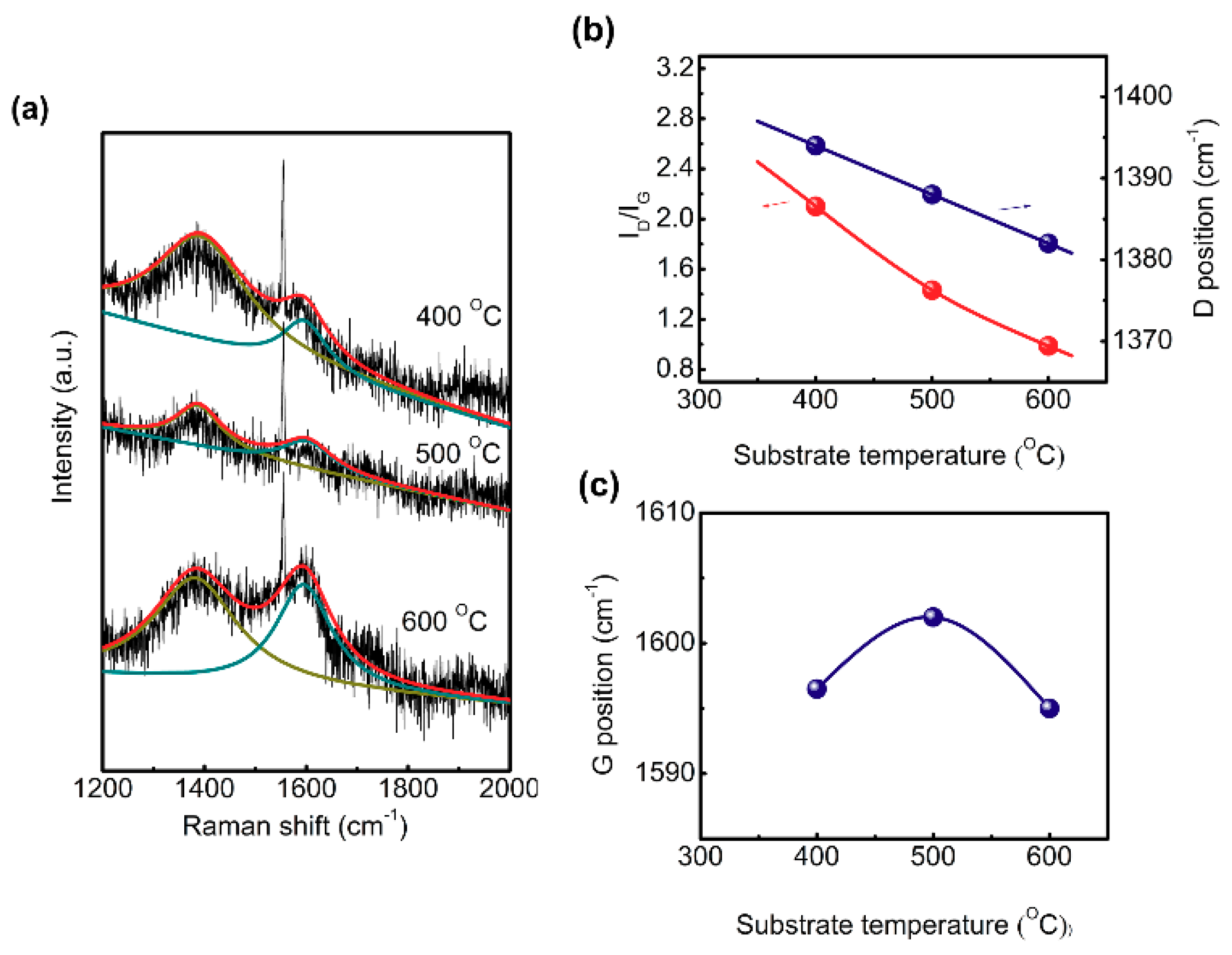
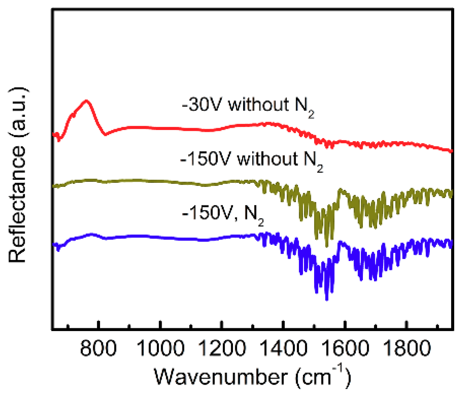
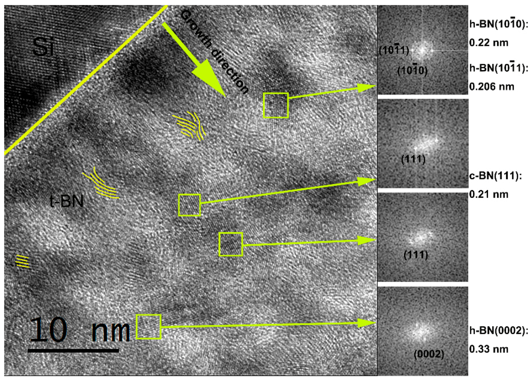
3. Results and Discussions

The BCN films with oriented crystalline h-BN nanodomains were prepared at various substrate temperatures in pure Ar gas on the Si substrate. The surface morphologies of these BCN films were inspected by SEM, indicating that the film surfaces become rougher with the increasing substrate temperature (Figure S1, Supplementary Materials). Column-like and even cone-like features emerge, especially for the film deposited at 600 °C. In order to observe the surface features more clearly, a cross sectional TEM image was taken for a film deposited with an r.f. power of 150 W and a bias voltage of −100 V at 600 °C, as illustrated in Figure 1a. The formation of a columnar structure with a conical surface can be clearly observed through the film growth direction. The thickness of this film is estimated as 175 nm. Figure 1b is a high-resolution TEM image taken from the selected area of the transition layer for this film. It exhibits one of the crystalline rod-like patches across the transition layer of a very high density. The width of these patches is about 5–18 nm, whilst the length is approximately 10–80 nm. The inset is the fast Fourier transformation (FFT) images of the selected area marked by the yellow square, which clearly shows the characteristic pattern of the normal orientation along the (0004) h-BN lattice planes, with an inter-planar distance of 0.186 nm at the entire regions of the patches. The lattice planes are slightly larger than that of the pure h-BN (0.167 nm), because of the C substitution. Figure 1c is a closer illustration of another selected area of the transition layer in this film. Figure 1d is the zoomed-in section of the selected area in Figure 1c, containing an inset of the h-BN atomic stacking model. From Figure 1d, the spacing of the adjacent white dots is 0.25 nm, corresponding to the nearest-distance between any of the same atoms of B or N within the chicken-wire layer [40]. It demonstrates a typical hexagonal symmetry, which indicates the single-crystalline nature within this crystalline domain. Figure 1e illustrates an image taken from the very top of the film, in which a thin layer of amorphous material covers the outermost film continuously. This amorphous layer is about 3–4 nm thick, following the conical surface up and down. Thus, from the TEM observations, it intuitively indicates that the BCN films prepared in the present case mainly consist of rod-like h-BN nanodomains, with the basal planes perpendicular to the substrate and homogeneously distributed across the film. The Raman spectroscopy is expected to elucidate the chemical bonding state of the as-synthesized BCN films. Figure 1f shows the Raman spectra for a typical BCN film on Si substrate at 600 °C, as well as commercial graphite, synthesized h-BN, and a silicon substrate wafer. The measurements were performed at room temperature with a Renishaw spectrometer at 473 nm, with notch filters cutting at ~100 cm−1. A tiny sharp peak at 1555 cm−1 was clearly present in the Raman spectrum of the BCN film, coming from the Si substrate, indicating that our BCN film was of a high transparency. As compared to the h-BN sample with only one sharp E2g peak at 1366 cm−1, the Raman spectrum of the BCN film closely resembled that of graphite. Two broad bands were observed at 1382 and 1595 cm−1, which are known as D and G band, respectively. The D band is usually assigned for distorted graphite, induced by the zone-boundary phonons activated by double resonance, and not just to the phonon confinement [41]. The G band corresponds to the E2g phonon at the Brillouin zone center [42], which is reported to be moving from 1580 to 1600 cm−1 [43]. Compared to the graphite sample, both the D and G bands of the BCN film blueshift and broaden to some certain extent. In the present case, the blueshift of the D band from 1366 to 1382 cm–1 is understood as a consequence of the lattice defects, as it requires a defect for its activation. The origin of the weak G band upshifts of ~3 cm–1 compared to the bulk graphite are partially due to the high hole doping induced phonon stiffening [43]. Our present BCN film contained a considerable amount of B, which will be discussed later. As the large downshift from 1600 to 1510 cm–1 of the G band generally occurs for a completely disordered, almost fully sp2-bonded amorphous carbon consisting of distorted six-fold rings, the loss of the three-dimensional ordering can be excluded in the present case [44]. Unlike the spectrum of graphite, the exclusive presence of the broad features in the region of the low Raman frequency of the BCN film are commonly found in the spectra of boron-rich materials [45]. This will be evident from the energy dispersive X-ray spectroscopy (EDXS) and XPS measurements in the following. Thus, based on the aforementioned information, the formation of BCN films with highly crystalline oriented h-BN nanodomains is obtained by r.f. magnetron sputtering at higher substrate temperatures.
FTIR was performed ex situ in order to discern the local bonding present and chemical environment within the films, as well as to detect IR-active film impurities. Figure 2 shows the FTIR spectra of the BCN films deposited using pure Ar under substrate temperatures varying from room temperature up to 600 °C. All of the spectra had been extracted by the referent Si (100) background. The referent h-BN showed two predominant peaks at around 770 and 1380 cm–1, representing the out-of-plane B–N–B bending vibration of a typical h-BN structure [46,47] and the in-plane B–N stretching vibration [48], respectively. However, the chemical bonding modification in BCN films is quite different. A peak located at around 1100 cm–1 was present in all of the spectra of the BCN films, induced by B–C bonds, which are usually found in B4C films [49]. The existence of this B–C bonds induced vibration absorption indicates the abundance of boron in the present films. Moreover, an additional broad absorption at ca 1250 cm–1 appeared for the film grown at room temperature, enhanced according to the substrate temperature, and finally overlapped with the in-plane B–N stretching peak at 1380 cm1. This broad IR absorption can be assigned to C–N bonds [50], implying that the carbon atomic content within the BCN films increases with the increasing substrate temperature. Moreover, the lack of a significant IR absorption at 1550 cm–1 indicates that the number of sp2 C=N bonds is below the equipment detection limit [51].
More interestingly, the activation of the h-BN IR peaks was observed only for the films grown in temperatures higher than 250 °C. The absence of the sp3 B–N normal stretching mode at 1080 cm–1 indicates the absence of the cubic phase of BN [48]. The out-of-plane B–N–B bending vibration at 770 cm−1 significantly enhances the intensity instead of the vanishing in-plane B–N stretching the vibration mode at 1380 cm−1, along with the increasing substrate temperature. Considering h-BN films with their basal planes perpendicular to the substrate surface (c-axis perpendicular to the surface normal), the out-of-plane bending mode should be preferentially excited by IR light at a normal incidence, as compared to the in-plane mode. Thus, the alignment of h-BN basal planes can be assessed by the IR peak intensity ratio of the out-of-plane mode to the in-plane mode [52]. As illustrated from Figure 2, the increased intensity ratio of the out-of-plane mode to the in-plane mode in our case strongly suggests that the h-BN domain in the BCN films becomes preferentially orientated with its hexagonal basal planes perpendicular to the substrate surface when increasing the substrate temperature.
Such relevance between the substrate temperature and the orientation of the h-BN nanodomains was further studied by Raman spectroscopy. In Figure 3a, the Raman spectra of the BCN films grown at 400, 500, and 600 °C show typical D and G bands at around 1380 and 1600 cm−1, respectively. Generally, a Raman D band of carbon materials originates from the finite crystal size of the lattice distortion [53]. The higher the number of defects, the higher the D band intensity. The ratio between the integral intensities of the D and G bands (ID/IG) is a measure of the degree of disorder in the BCN films. The ID/IG value decreases monotonously as the substrate temperature increases, as shown in Figure 3b, suggesting an increased h-BN nanodomain size [54]. For the samples grown at lower temperatures, a relatively higher degree of disorder is obtained for ID/IG. It also explains the failure in the detection of the Raman signal for the samples grown at lower temperatures (<250 °C). The defect density and h-BN nanodomain crystallite size are also determined using the ID/IG ratio [55], as listed in Table 1. A defect density of the order of 1011 cm−2 is estimated for these BCN films, which can be attributed to the grain boundaries and structural defects. When the substrate temperature increases during film growth, the defect density decreases by one order of magnitude. This is further evidenced by an increase in the h-BN nanodomain crystallite size of 91 nm, which is well in line with the TEM results. This points towards an obvious correlation that a higher substrate is beneficial to the growth of the crystalline h-BN nanodomains. Additionally, both the D and G band shift can also provide further information on the degree of disorder in the BCN films. As can be seen in Figure 3b (right Y scale), the shift of the D peak position becomes less as the substrate temperature increases compared with that of the graphite sample (1366 cm−1), strongly suggesting a lower degree of disorder and better crystallinity in the BCN films at higher temperatures. As for the G peak, its position moves to the higher frequency in these samples, however in a fluctuating manner, as shown in Figure 3c. Indeed, in the materials containing only sp2 hexagonal rings, the shift of G peak saturates at around 1600 cm−1, which is a typical G position in nanocrystalline-graphite [43]. Thus, in conjunction with TEM and FTIR, the Raman spectra demonstrate that the h-BN nanodomains exhibit a vertical alignment of the basal planes in the BCN films, with improved ordering at a higher substrate temperature.
A higher substrate temperature in combination with a moderate energetic ion bombardment has been suggested to play a predominant role in growing vertically oriented h-BN basal planes [48]. In the case of the physical vapor deposition (PVD) method, a negative bias voltage applied during the film growth controls the ion energy, which actually results in the densification of the h-BN planes. A higher temperature, which induces a high atomic mobility, compensates the densification process by diffusing the atoms nearby. Based on this scenario, a situation of a high temperature and high bias voltage should be expected for the synthesis of vertically aligned h-BN films with its basal planes. However, as shown in Figure 4, for the BCN films deposited at 500 °C at a lower bias (−30 V), the out-of-plane B–N–B bending vibration at 770 cm−1 enhances in intensity as compared to the film deposited at a higher bias (−150 V), with other growth parameters remaining the same. A great improvement of the ordered h-BN fraction in the BCN films is evident for I780/I1380, which is higher at a lower bias. Bearing in mind that the large fraction of the amorphous background probably provides a local relaxed environment for these h-BN nanodomains, this contradiction strongly indicates that the significant preferential orientation of the h-BN basal planes here may be due to a preferential displacement [56] or to kinetic conditions favoring the lowest Gibbs free energy, in which the c axis parallels to the surface [57]. In fact, a larger basal plane spacing of the h-BN nanodomains deposited at higher bias (Figure 1) than that of crystalline h-BN has been observed, in accordance with the carbon films obtained by Lifshitz et al. [58].
Furthermore, the usage of N2 in the working gas is generally expected to replenish the deficiency of N in the film deposited with the sputtering method, aiming at an improved crystallinity. However, adding N2 into the working gas (Ar/N2 = 50 sccm/50 sccm) at a bias of −150 V, with the other parameters remaining fixed, the out-of-plane B–N–B vibration is negligibly changed, as observed in Figure 4. Thus, the involvement of the N2 flow into Ar gas seemingly disturbs the growth of the h-BN nanodomains in the BCN films. This result is distinct from the previous report, where the addition of N2 is beneficial for achieving h-BN basal planes parallel to the surface [59].
In order to discern the effects of N2 on the film morphology, BCN films prepared on the Si (100) substrate at a deposition temperature of 500 °C with a different N2/Ar gas flow ratio were characterized by SEM. As shown in Figure S2 (Supplementary Materials), the surface morphologies of the BCN films are smooth and continuous in a large-scale area, regardless of the N2/Ar gas ratio. Therefore, the microstructure of a film prepared with a N2/Ar gas flow ratio of 1 was investigated by HRTEM. Figure 5 shows that turbostratic BN (t-BN) planes with a random orientation are formed within the BCN film matrix, as well as a tiny amount of BN nanocrystals (2–6 nm). As we know, t-BN is an analog to h-BN, but with randomly oriented basal planes. Unlike the vertically aligned h-BN nanodomains formed in the large background of amorphous BCN, the almost complete elimination of the amorphous fraction inside the film with the addition of N2 lead to a higher kinetic condition, which may play an important role in the h-BN/c-BN phase equilibrium [60]. Under such a kinetic condition, the atomic mobility increased by high substrate temperatures is not sufficient enough to allow for the local bombardment-induced densifications to relax back to the thermodynamically stable h-BN phase. The h-BN/c-BN nucleation environment is gradually shifting. The formation of the curved and/or tilted t-BN basal planes observed here significantly prevents the growth of vertically oriented h-BN basal planes. In fact, these defective t-BN plane edges serve as c-BN nucleation sites as a result of the sp3 character of the B–N–B bonds in the curled sp2 bonded sheets [56].
Furthermore, the chemical composition of the as-obtained BCN films at various temperatures without N2, and at various N2/Ar flow ratios are analyzed by their corresponding EDXS (marked by balls) as compared with the surface composition estimated from the XPS (marked by crosses), as shown in Figure 6a. For the system of BCN films prepared at different substrate temperatures, the EDXS results indicate that the deposited films of all of the sets are boron rich, confirming the earlier observation. However, a deviation of 60% of the surface composition from the bulk composition is obtained for the C content, while the B/N ratios stay nearly the same. This surface composition shift towards C can be due to the deposition process and the adsorption of hydrocarbons during the transportation from the preparation chamber to the analysis chamber [61]. Nevertheless, one can conclude that the carbon content in the system of the BCN films containing aligned h-BN nanodomains monotonously increases with the increasing temperature, which indicates that the carbon content can be controlled. On the other hand, the system of BCN films with randomly oriented t-BN nanocrystals prepared with mixed N2/Ar exhibits elemental contents. Unfortunately, the C content in this system of samples fluctuates with the increasing N2/Ar flow ratio, although with a relatively high B-content.
The bonding structure and surface composition of the BCN films with oriented h-BN nanodomains and mixed t-BN nanodomains (without and with N2) was further analyzed by XPS. By deconvolution using a mixed Lorentzian (80%)–Gaussian (20%) fitting after a Shirley-type background subtraction, the XPS core level spectra of the B1s, C1s, and N1s peaks of the BCN films are depicted in Figure 6b. For the BCN film deposited without N2, the B1s are deconvoluted into four component peaks centered at 187.8, 189.5, 190.5, and 191.9 eV, respectively. The peak at 187.8 eV is attributed to the B–B bond [51]. An apparent shoulder peak located at 189.5 eV suggests the contribution of a B–C bond in the C-rich environment [62]. The peak at 191.9 eV is attributed to the B–O bond [4]. The peaks at 190.5 eV can be assigned to the sp2 B–N bond in h-BN [63], which shifts a little to the higher energy, owing to the higher electronegativity of oxygen to the boron. The XPS results confirm that B is rich in the BCN films deposited without N2. In addition, B atoms are chemically bonded with both N and C atoms in the present case. The spectra of C1s were deconvoluted into four binding states located at 284.3, 284.6, 285.7, and 288.3 eV, which can be assigned to the C–B bond, C–C bond, C–N bond, and C–O bond, respectively [13,35,64]. The fitted peaks of the N1s core level spectra located at 397.8 and 398.8 eV, are attributed to the sp2 N–B bond (h-BN) and N–C bond, respectively [1,65]. The existence of B–N, B–C, and C–N bonds confirms that the films obtained in this study are composed of hybridized B–C–N bonding. Furthermore, both of the fitting results of the B1s and N1s core level spectra demonstrate that the BCN film deposited without N2 is mainly the sp2 hexagonal phase, which is in good accordance with the above results. For the BCN film deposited with N2/Ar, besides the B–C bond and sp2 B–N bond at 189.5 and 190.3 eV, an additional component peak appears at 191.1 eV, which can be attributed to the sp3 B–N bond [63]. C1s have also been deconvoluted into four binding states, including the C–B bond, C–C bond, C–N bond, and C–O bond. Similar to B1s, a sp3 N-B bond newly appears at 398.4 eV at the N1s deconvolution spectra [66], together with the sp2 N–B bond and the N–C bond located at 397.7 and 398.8 eV, respectively. Compared to the oriented BCN film without N2, the intensities of the B1s and N1s core level spectra significantly increased, while the C1s decreased. As a result of the addition of nitrogen, the B–B bonds and B–O bonds disappear, and the B–N (N–B) bonds increase, which might be induced by the N atoms preferentially binding to the B atoms to form BN [29,67,68]. As a result, the thickness of the outermost amorphous layer is reduced after the addition of nitrogen.
The UV-Vis absorption spectrum was used to investigate the optical energy gap of the BCN films, owing to the optically induced transitions. The substrate background was subtracted using a blank reference. The optical band gap was determined by Tauc’s equation [13,14]. The extrapolation of the linear region of the Tauc plot to intercept on the x-axis led to the optical bandgap (Eopt) values for the material. Figure 7 provides the UV-Vis optical absorption spectra of two types of BCN films containing vertically oriented h-BN nanodomains prepared without N2 at different temperatures, and mixed t-BN with N2 and their corresponding Tauc plots. As seen from Figure 7a, the film grown with N2 exhibits a unique absorption peak at around 248 nm (5.0 eV), indicating both the structural and chemical uniformity of the BCN films. On the other hand, it exhibits two absorption peaks (2.6 and 4.1 eV) for the film prepared without N2, which could be related to the new transition pathways introduced as a result of the formation of the oriented h-BN domains in the matrix of amorphous BCN. The absorption at 2.6 eV can be ascribed to the transition pathways between the C–N π-conduction band and the long pair (LP) state of the bridge nitride atom, or between the conduction band and the valence band for the C–N π-band, while the other probably corresponds to that between the conduction band and the valence band for the C–N σ band [69]. A broad hump at around 220 nm (5.63 eV) appears for the film grown at 500 °C, and becomes sharper and more intense for the films grown at higher temperatures, in which the h-BN domain crystallites grow. This peak corresponds to the optical absorption gap energy of the typical h-BN phase [15,70], which is smaller than that of the crystalline h-BN, probably because of the doping of C or the boundary effect. From Figure 7b, one can also trace the band edge absorptions of the BCN matrix and the oriented h-BN domains. The observation of the h-BN optical bandgap in this type of film indicates that both the h-BN nanodomains and amorphous BCN matrix are large enough to maintain their individual bandgaps. Assuming that each embedded h-BN nanodomain acts as a separated infinite “hole” within the BCN film, this actually provides a possibility to monitor the Eopt via adjusting the carbon content and/or the microstructure, as the h-BN nanodomains and amorphous hybridized BCN fraction can be clearly phase-separated.
Figure 8a shows the band edge absorptions with respect to the carbon content in the BCN films containing vertically oriented h-BN domains. With an increase in the carbon concentration, the optical band gap corresponding to the h-BN domains is apparently constant at around 5.6 eV. On the contrary, both of the optical band edges from the BCN matrix shift to the low-energy side, in accordance with previous observation in amorphous C:N films and diamond like carbon, respectively [71,72]. This is probably correlated with the B and/or N substation for the C atoms, and/or because of the impact of the h-BN domains incorporation on the band structure of the BCN films. It is evident that the crystalline h-BN nanodomains become larger with the increasing substrate temperature increases (C content increases). The enhancement in the doping effect is in line with the XPS results, where more B–C and N–C bonds were observed for the higher C content samples. Assuming the huge fraction of BCN background as a uniform ternary compound, the optical band absorption values of the BCN films can be considered as a linear decrease in the bandgap from h-BN and amorphous carbon, intermediate to those of amorphous BC (2.1 eV) [14] and CNx (2–3.8 eV) [71], as shown in Figure 8a.
On the other hand, it should be mentioned that the band absorption value of the uniformed mixed BCN films is not sensitive to the carbon content, as seen in the inset of Figure 8a, implying that structural factors also count on the band gap, rather than carbon content. In fact, for the BCN films with specific microstructures, the carbon content cannot simply rely on the incorporation of N2, because of the nitridation of the target in the growth process. During the growth, the increased N2 incorporation for the gas phase may suppress the growth rate, leading to a saturation of carbon content in the films.
Thus, a ternary B–C–N diagram is summarized in Figure 8b, where the BxCyNz films synthesized in the present work are recorded together with those classic compounds. The carbon content can be adjusted by the growth kinetics, that is, temperature (marked by red balls), by fixing the B/N ratio. Based on these band gap value measurements, it strongly indicates that, for a given stoichiometry, the electronic and optical properties of the BCN films can be engineered by feasible growth conditions.

4. Conclusions

In summary, we have synthesized hybridized BCN films consisting of rod-like crystalline h-BN nanodomains, with its basal planes perpendicular to the substrate, demonstrating the structural evolution and optical band gap that have been controlled via growth kinetics. The amorphous BCN matrix serves as a special thermodynamic environment for growing an oriented crystalline h-BN phase, which is a non-energetic process contrary to the usually reported phase. The formation of h-BN nanodomains acts as infinite “holes” separated by the BCN matrix, exhibiting different optical band gap values from the BCN matrix, which decrease as the carbon content increases in the BCN matrix, as a result of the doping and/or boundary effect. This form of hybridized BCN system with a certain band gap and composition may be tailored to design the 3D semiconducting building blocks not only for fundamental physics, but also to be applied in the field of future optics, electronics, and energy conversion and storage devices.

Supplementary Materials

The following are available online at https://www.mdpi.com/2079-6412/9/3/185/s1, Figure S1: SEM images of the samples prepared in pure Ar with various substrate temperatures at (a) 250, (b) 400, (c) 500, and (d) 600 °C. The images of (e) and (f) are the samples prepared in pure Ar with a substrate temperature at (c) 500 and (d) 600 °C, respectively, collected with the sample tilting in an angle of 45° toward the SEM detector, Figure S2: SEM images of the samples prepared at substrate temperature of 500 °C with different N2/Ar gas ratios of 0 (a), 0.2 (b), 0.4 (c), 0.6 (d), 0.8 (e), and 1 (f).

Author Contributions

Conceptualization, H.Y.; Data Curation, Y.L. and H.Y.; Formal Analysis, Y.L., W.G., F.W., D.Z., Y.Z., and H.Y.; Methodology, F.W.; Supervision, H.Y.; Writing—Original Draft, Y.L., W.G., and H.Y.

Funding

This research was funded by the National Natural Science Foundation of China (Nos. 51572105, 61504046 and 51872113).

Acknowledgments

H. Yin is grateful to the Scientific Research Foundation for the Returned Overseas Chinese Scholars, the State Education Ministry. The financial support from the Scientific Research Foundation for the Returned Overseas Scholars of Jilin Province is also appreciated.

Conflicts of Interest

The authors declare no conflict of interest.

References

  1. Song, L.; Liu, Z.; Reddy, A.L.; Narayanan, N.T.; Taha-Tijerina, J.; Peng, J.; Gao, G.; Lou, J.; Vajtai, R.; Ajayan, P.M. Binary and ternary atomic layers built from carbon, boron, and nitrogen. Adv. Mater. 2012, 24, 4878–4895. [Google Scholar] [CrossRef]
  2. Paraknowitsch, J.P.; Thomas, A. Doping carbons beyond nitrogen: an overview of advanced heteroatom doped carbons with boron, sulphur and phosphorus for energy applications. Energy Environ. Sci. 2013, 6, 2839. [Google Scholar] [CrossRef] [Green Version]
  3. Zeng, Q.; Wang, H.; Fu, W.; Gong, Y.; Zhou, W.; Ajayan, P.M.; Lou, J.; Liu, Z. Band engineering for novel two-dimensional atomic layers. Small 2015, 11, 1868–1884. [Google Scholar] [CrossRef]
  4. Byon, E.; Son, M.; Lee, K.-H.; Nam, K.-S.; Hara, N.; Sugimoto, K. Electrochemical properties of boron–carbon–nitride films formed by magnetron sputtering. Electrochim. Acta 2006, 51, 2662–2668. [Google Scholar] [CrossRef]
  5. Zhao, Y.; He, D.W.; Daemen, L.L.; Shen, T.D.; Schwarz, R.B.; Zhu, Y.; Bish, D.L.; Huang, J.; Zhang, J.; Shen, G.; et al. Superhard B–C–N materials synthesized in nanostructured bulks. J. Mater. Res. 2011, 17, 3139–3145. [Google Scholar] [CrossRef]
  6. Prakash, A.; Todi, V.; Sundaram, K.B.; Ross, L.; Xu, G.H.; French, M.; Henry, P.; King, S.W. Investigation of the dielectric and mechanical properties for magnetron sputtered BCN thin films. ECS J. Solid State Sci. Technol. 2015, 4, N3122–N3126. [Google Scholar] [CrossRef]
  7. Yue, J.S.; Cheng, W.J.; Zhang, X.W.; He, D.Y.; Chen, G.H. Ternary BCN thin films deposited by reactive sputtering. Thin Solid Films 2000, 375, 247–250. [Google Scholar] [CrossRef]
  8. Beniwal, S.; Hooper, J.; Miller, D.P.; Costa, P.S.; Chen, G.; Liu, S.Y.; Dowben, P.A.; Sykes, E.C.; Zurek, E.; Enders, A. Graphene-like boron-carbon-nitrogen monolayers. ACS Nano 2017, 11, 2486–2493. [Google Scholar] [CrossRef]
  9. Umeda, S.; Yuki, T.; Sugiyama, T.; Sugino, T. Boron carbon nitride film with low dielectric constant as passivation film for high speed electronic devices. Diam. Relat. Mater. 2004, 13, 1135–1138. [Google Scholar] [CrossRef]
  10. Prakash, A.; Sundaram, K.B.; Campiglia, A.D. Photoluminescence studies on BCN thin films synthesized by RF magnetron sputtering. Mater. Lett. 2016, 183, 355–358. [Google Scholar] [CrossRef]
  11. Prakash, A.; Nehate, S.D.; Sundaram, K.B. Boron carbon nitride based metal-insulator-metal UV detectors for harsh environment applications. Opt. Lett. 2016, 41, 4249–4252. [Google Scholar] [CrossRef]
  12. Wan, S.; Yu, Y.; Pu, J.; Lu, Z. Facile fabrication of boron nitride nanosheets–amorphous carbon hybrid film for optoelectronic applications. RSC Adv. 2015, 5, 19236–19240. [Google Scholar] [CrossRef]
  13. Prakash, A.; Sundaram, K.B. Optical and XPS studies of BCN thin films by co-sputtering of B4C and BN targets. Appl. Surf. Sci. 2017, 396, 484–491. [Google Scholar] [CrossRef]
  14. Todi, V.O.; Shantheyanda, B.P.; Sundaram, K.B. Influence of annealing on the optical properties of reactively sputtered BCN thin films. Mater. Chem. Phys. 2013, 141, 596–601. [Google Scholar] [CrossRef]
  15. Todi, V.O.; Shantheyanda, B.P.; Todi, R.M.; Sundaram, K.B.; Coffey, K. Optical characterization of BCN films deposited at various N2/Ar gas flow ratios by RF magnetron sputtering. Mater. Sci. Eng. B-Adv. Funct. Solid-State Mater. 2011, 176, 878–882. [Google Scholar] [CrossRef]
  16. Kim, S.Y.; Park, J.; Choi, H.C.; Ahn, J.P.; Hou, J.Q.; Kang, H.S. X-ray photoelectron spectroscopy and first principles calculation of BCN nanotubes. J. Am. Chem. Soc. 2007, 129, 1705–1716. [Google Scholar] [CrossRef] [PubMed]
  17. Ci, L.; Song, L.; Jin, C.H.; Jariwala, D.; Wu, D.X.; Li, Y.J.; Srivastava, A.; Wang, Z.F.; Storr, K.; Balicas, L.; et al. Atomic layers of hybridized boron nitride and graphene domains. Nat. Mater. 2010, 9, 430–435. [Google Scholar] [CrossRef]
  18. Krivanek, O.L.; Chisholm, M.F.; Nicolosi, V.; Pennycook, T.J.; Corbin, G.J.; Dellby, N.; Murfitt, M.F.; Own, C.S.; Szilagyi, Z.S.; Oxley, M.P.; et al. Atom-by-atom structural and chemical analysis by annular dark-field electron microscopy. Nature 2010, 464, 571–574. [Google Scholar] [CrossRef] [PubMed]
  19. Shirodkar, S.N.; Waghmare, U.V.; Fisher, T.S.; Grau-Crespo, R. Engineering the electronic bandgaps and band edge positions in carbon-substituted 2D boron nitride: a first-principles investigation. Phys. Chem. Chem. Phys. 2015, 17, 13547–13552. [Google Scholar] [CrossRef] [PubMed] [Green Version]
  20. Zhang, M.; Gao, G.Y.; Kutana, A.; Wang, Y.C.; Zou, X.L.; Tse, J.S.; Yakobson, B.I.; Li, H.D.; Liu, H.Y.; Ma, Y.M. Two-dimensional boron-nitrogen-carbon monolayers with tunable direct band gaps. Nanoscale 2015, 7, 12023–12029. [Google Scholar] [CrossRef] [PubMed]
  21. Banerjee, S.; Pati, S.K. Criticality of surface topology for charge-carrier transport characteristics in two-dimensional borocarbonitrides: design principles for an efficient electronic material. Nanoscale 2014, 6, 13430–13434. [Google Scholar] [CrossRef] [PubMed]
  22. Zhou, Z.F.; Bello, I.; Lei, M.K.; Li, K.Y.; Lee, C.S.; Lee, S.T. Synthesis and characterization of boron carbon nitride films by radio frequency magnetron sputtering. Surf. Coat. Technol. 2000, 128, 334–340. [Google Scholar] [CrossRef]
  23. Wada, Y.; Yap, Y.K.; Yoshimura, M.; Mori, Y.; Sasaki, T. The control of B–N and B–C bonds in BCN films synthesized using pulsed laser deposition. Diam. Relat. Mater. 2000, 9, 620–624. [Google Scholar] [CrossRef]
  24. Sugino, T.; Hieda, H. Field emission characteristics of boron carbon nitride films synthesized by plasma-assisted chemical vapor deposition. Diam. Relat. Mater. 2000, 9, 1233–1237. [Google Scholar] [CrossRef]
  25. Mannan, M.A.; Baba, Y.; Kida, T.; Nagano, M.; Shimoyama, I.; Hirao, N.; Noguchi, H. Orientation of B–C–N hybrid films deposited on Ni (111) and polycrystalline Ti substrates explored by X-ray absorption spectroscopy. Thin Solid Films 2011, 519, 1780–1786. [Google Scholar] [CrossRef]
  26. Hasegawa, T.; Yamamoto, K.; Kakudate, Y. Synthesis of B–C–N thin films by electron beam excited plasma CVD. Diam. Relat. Mater. 2002, 11, 1290–1294. [Google Scholar] [CrossRef]
  27. Caretti, I.; Jiménez, I.; Gago, R.; Cáceres, D.; Abendroth, B.; Albella, J.M. Tribological properties of ternary BCN films with controlled composition and bonding structure. Diam. Relat. Mater. 2004, 13, 1532–1537. [Google Scholar] [CrossRef]
  28. Laidani, N.; Anderle, M.; Canteri, R.; Elia, L.; Luches, A.; Martino, M.; Micheli, V.; Speranza, G. Structural and compositional study of B–C–N films produced by laser ablation of B4C targets in N2 atmosphere. Appl. Surf. Sci. 2000, 157, 135–144. [Google Scholar] [CrossRef]
  29. Kosaka, M.; Urakami, N.; Hashimoto, Y. Formation of graphitic carbon nitride and boron carbon nitride film on sapphire substrate. Jpn. J. Appl. Phys. 2018, 57, 02CB09. [Google Scholar] [CrossRef]
  30. Tsai, P.-C. The deposition and characterization of BCN films by cathodic arc plasma evaporation. Surf. Coat. Technol. 2007, 201, 5108–5113. [Google Scholar] [CrossRef]
  31. Bengu, E.; Genisel, M.F.; Gulseren, O.; Ovali, R. Theoretical and spectroscopic investigations on the structure and bonding in B–C–N thin films. Thin Solid Films 2009, 518, 1459–1464. [Google Scholar] [CrossRef] [Green Version]
  32. Jiang, X.; Zhuang, C.Q.; Li, X.Q.; Sai, L.W.; Zhao, J.J.; Jiang, X. Mapping distributions of mechanical properties and formation ability on the ternary B–C–N phase diagram. Diam. Relat. Mater. 2011, 20, 891–895. [Google Scholar] [CrossRef]
  33. Park, J.K.; Ko, J.S.; Baik, Y.J. Effect of hydrogen addition on the residual stress of B–C–N films with cubic boron nitride phase prepared by r.f. magnetron sputtering of a B4C target. Surf. Coat. Technol. 2013, 215, 104–109. [Google Scholar] [CrossRef]
  34. Tavsanoglu, T.; Jeandin, M.; Addemir, O. Synthesis and characterisation of thin films in the B–C–N triangle. Surf. Eng. 2016, 32, 755–760. [Google Scholar] [CrossRef]
  35. Prakash, A.; Sundaram, K.B. Deposition and XPS studies of dual sputtered BCN thin films. Diam. Relat. Mater. 2016, 64, 80–88. [Google Scholar] [CrossRef]
  36. Pakdel, A.; Wang, X.; Zhi, C.; Bando, Y.; Watanabe, K.; Sekiguchi, T.; Nakayama, T.; Golberg, D. Facile synthesis of vertically aligned hexagonal boron nitride nanosheets hybridized with graphitic domains. J. Mater. Chem. 2012, 22, 4818. [Google Scholar] [CrossRef]
  37. Giovannetti, G.; Khomyakov, P.A.; Brocks, G.; Kelly, P.J.; van den Brink, J. Substrate-induced band gap in graphene on hexagonal boron nitride: Ab initio density functional calculations. Phys. Rev. B 2007, 76. [Google Scholar] [CrossRef] [Green Version]
  38. Bepete, G.; Voiry, D.; Chhowalla, M.; Chiguvare, Z.; Coville, N.J. Incorporation of small BN domains in graphene during CVD using methane, boric acid and nitrogen gas. Nanoscale 2013, 5, 6552–6557. [Google Scholar] [CrossRef]
  39. Vijayakumar, A.; Todi, R.M.; Warren, A.P.; Sundaram, K.B. Influence of N2/Ar gas mixture ratio and annealing on optical properties of SiCBN thin films prepared by rf sputtering. Diam. Relat. Mater. 2008, 17, 944–948. [Google Scholar] [CrossRef]
  40. Zhi, C.Y.; Bando, Y.; Tang, C.C.; Kuwahara, H.; Golberg, D. Large-scale fabrication of boron nitride nanosheets and their utilization in polymeric composites with improved thermal and mechanical properties. Adv. Mater. 2009, 21, 2889. [Google Scholar] [CrossRef]
  41. Ferrari, A.C.; Meyer, J.C.; Scardaci, V.; Casiraghi, C.; Lazzeri, M.; Mauri, F.; Piscanec, S.; Jiang, D.; Novoselov, K.S.; Roth, S.; et al. Raman spectrum of graphene and graphene layers. Phys. Rev. Lett. 2006, 97. [Google Scholar] [CrossRef]
  42. Yu, J.; Wang, E.G.; Ahn, J.; Yoon, S.F.; Zhang, Q.; Cui, J.; Yu, M.B. Turbostratic boron carbonitride films produced by bias-assisted hot filament chemical vapor deposition. J. Appl. Phys. 2000, 87, 4022–4025. [Google Scholar] [CrossRef]
  43. Ferrari, A.C. Raman spectroscopy of graphene and graphite: Disorder, electron–phonon coupling, doping and nonadiabatic effects. Solid State Commun. 2007, 143, 47–57. [Google Scholar] [CrossRef]
  44. Li, F.; Lannin, J.S. Radial distribution function of amorphous carbon. Phys. Rev. Lett. 1990, 65, 1905–1908. [Google Scholar] [CrossRef]
  45. Beckel, C.L.; Yousaf, M.; Fuka, M.Z.; Raja, S.Y.; Lu, N. Lattice vibrations of the icosahedral solid alpha-boron. Phys. Rev. B 1991, 44, 2535. [Google Scholar] [CrossRef]
  46. Linss, V.; Hermann, I.; Schwarzer, N.; Kreissig, U.; Richter, F. Mechanical properties of thin films in the ternary triangle B–C–N. Surf. Coat. Technol. 2003, 163, 220–226. [Google Scholar] [CrossRef]
  47. Qu, J.; Li, Q.; Luo, C.; Cheng, J.; Hou, X. Characterization of flake boron nitride prepared from the low temperature combustion synthesized precursor and its application for dye adsorption. Coatings 2018, 8, 214. [Google Scholar] [CrossRef]
  48. Cometto, O.; Sun, B.; Tsang, S.H.; Huang, X.; Koh, Y.K.; Teo, E.H.T. Vertically self-ordered orientation of nanocrystalline hexagonal boron nitride thin films for enhanced thermal characteristics. Nanoscale 2015, 7, 18984–18991. [Google Scholar] [CrossRef]
  49. Pascual, E.; MartíNez, E.; Esteve, J.; Lousa, A. Boron carbide thin films deposited by tuned-substrate RF magnetron sputtering. Diam. Relat. Mater. 1999, 8, 402–405. [Google Scholar] [CrossRef]
  50. Yap, Y.K.; Kida, S.; Aoyama, T.; Mori, Y. Influence of negative dc bias voltage on structural transformation of carbon nitride at 600 °C. Appl. Phys. Lett. 1998, 73, 915–917. [Google Scholar] [CrossRef]
  51. Nakao, S.; Sonoda, T.; Tsugawa, K.; Choi, J.; Kato, T. Effects of nitrogen gas ratio on composition and microstructure of BCN films prepared by RF magnetron sputtering. Vacuum 2009, 84, 642–647. [Google Scholar] [CrossRef]
  52. Higashi, G.S.; Chabal, Y.J.; Trucks, G.W.; Raghavachari, K. Ideal hydrogen termination of the Si (111) surface. Appl. Phys. Lett. 1990, 56, 656–658. [Google Scholar] [CrossRef]
  53. Cheng, Y.; Zhang, Q.; Fang, C.; Chen, J.; Su, J.; Xu, K.; Ai, L.; Liu, D. Preparation, structure, and properties of surface modified graphene/epoxy resin composites for potential application in conductive ink. Coatings 2018, 8, 387. [Google Scholar] [CrossRef]
  54. Chang, C.K.; Kataria, S.; Kuo, C.C.; Ganguly, A.; Wang, B.Y.; Hwang, J.Y.; Huang, K.J.; Yang, W.H.; Wang, S.B.; Chuang, C.H. Band gap engineering of chemical vapor deposited graphene by in situ BN doping. ACS Nano 2013, 7, 1333–1341. [Google Scholar] [CrossRef] [PubMed]
  55. Cancado, L.G.; Jorio, A.; Ferreira, E.H.M.; Stavale, F.; Achete, C.A.; Capaz, R.B.; Moutinho, M.V.O.; Lombardo, A.; Kulmala, T.S.; Ferrari, A.C. Quantifying defects in graphene via Raman spectroscopy at different excitation energies. Nano Lett. 2011, 11, 3190–3196. [Google Scholar] [CrossRef]
  56. Li, Q.; Marks, L.D.; Lifshitz, Y.; Lee, S.T.; Bello, I. Controlling the nucleation environment of c-BN films and their related properties. Phys. Rev. B 2002, 65. [Google Scholar] [CrossRef]
  57. Mckenzie, D.R.; Mcfall, W.D.; Sainty, W.G.; Davis, C.A.; Collins, R.E. Compressive stress induced formation of cubic boron nitride. Diam. Relat. Mater. 1993, 2, 970–976. [Google Scholar] [CrossRef]
  58. Lifshitz, Y.; Meng, X.M.; Lee, S.T.; Akhveldiany, R.; Hoffman, A. Visualization of diamond nucleation and growth from energetic species. Phys. Rev. Lett. 2004, 93. [Google Scholar] [CrossRef]
  59. Anutgan, M.; Anutgan, T.A.; Ozkol, E.; Atilgan, I.; Katircioglu, B. Influence of the nitrogen flow rate on the order and structure of PECVD boron nitride thin films. J. Non-Cryst. Solids 2009, 355, 1622–1629. [Google Scholar] [CrossRef]
  60. Hofsäss, H.; Feldermann, H.; Eyhusen, S.; Ronning, C. Fundamental role of ion bombardment for the synthesis of cubic boron nitride films. Phys. Rev. B 2002, 65, 115410. [Google Scholar] [CrossRef]
  61. Linss, V.; Rodil, S.E.; Reinke, P.; Garnier, M.G.; Oelhafen, P.; Kreissig, U.; Richter, F. Bonding characteristics of DC magnetron sputtered B–C–N thin films investigated by Fourier-transformed infrared spectroscopy and X-ray photoelectron spectroscopy. Thin Solid Films 2004, 467, 76–87. [Google Scholar] [CrossRef]
  62. Puyoo, G.; Teyssandier, F.; Pailler, R.; Labrugere, C.; Chollon, G. Boron carbonitride coatings synthesized by LPCVD, structure and properties. Carbon 2017, 122, 19–46. [Google Scholar] [CrossRef]
  63. Jia, F.; Zhuang, C.; Guan, C.; Zhao, J.; Bai, Y.; Jiang, X. Preparation of B–C–N films by magnetron sputtering with different N2/Ar flow ratio. Vacuum 2011, 85, 887–891. [Google Scholar] [CrossRef]
  64. Kang, Y.; Chu, Z.Y.; Zhang, D.J.; Li, G.Y.; Jiang, Z.H.; Cheng, H.F.; Li, X.D. Incorporate boron and nitrogen into graphene to make BCN hybrid nanosheets with enhanced microwave absorbing properties. Carbon 2013, 61, 200–208. [Google Scholar] [CrossRef]
  65. Lei, M.K.; Li, Q.; Zhou, Z.F.; Bello, I.; Lee, C.S.; Lee, S.T. Characterization and optical investigation of BCN film deposited by RF magnetron sputtering. Thin Solid Films 2001, 389, 194–199. [Google Scholar] [CrossRef]
  66. Xu, S.; Ma, X.; Tang, G.; Zhang, Q. Air annealing effect on scratch behaviour of BCN films. Surf. Eng. 2015, 31, 549–555. [Google Scholar] [CrossRef]
  67. Zhang, S.; Wu, J.; Yang, Q.; Tu, R.; Wang, C.; Shen, Q.; Zhang, L. Stoichiometric controlling of boroncarbonitride thin films with using BN-C dual-targets. AIP Adv. 2015, 5, 047125. [Google Scholar] [CrossRef] [Green Version]
  68. Yamamoto, K.; Keunecke, M.; Bewilogua, K.; Czigany, Z.; Hultman, L. Structural features of thick c-boron nitride coatings deposited via a graded B–C–N interlayer. Surf. Coat. Technol. 2001, 142, 881–888. [Google Scholar] [CrossRef]
  69. Yuan, Y.W.; Zhang, L.L.; Xing, J.; Utama, M.I.B.; Lu, X.; Du, K.Z.; Li, Y.M.; Hu, X.; Wang, S.J.; Genc, A.; et al. High-yield synthesis and optical properties of g-C3N4. Nanoscale 2015, 7, 12343–12350. [Google Scholar] [CrossRef]
  70. Watanabe, K.; Taniguchi, T.; Kanda, H. Direct-bandgap properties and evidence for ultraviolet lasing of hexagonal boron nitride single crystal. Nat. Mater. 2004, 3, 404–409. [Google Scholar] [CrossRef]
  71. Ech-chamikh, E.; Essafti, A.; Azizan, M.; Ijdiyaou, Y. Optical characterization of a-C:N thin films deposited by RF sputtering. Sol. Energy Mater. Sol. Cells 2006, 90, 1424–1428. [Google Scholar] [CrossRef]
  72. Shi, J.R.; Wang, J.P. Diamond-like carbon films prepared by facing-target sputtering. Thin Solid Films 2002, 420, 172–176. [Google Scholar] [CrossRef]
Figure 1. (a) Cross-sectional TEM images of a typical boron carbonitride (BCN) film deposited at 600 °C in pure Ar on a Si substrate; (b) High-resolution TEM (HRTEM) image taken from the selected area of the transition layer for the same film, the inset is the fast Fourier transformation (FFT) pattern of the single-crystalline region; (c) HRTEM image taken from another selected area; (d) A closer HRTEM image of the selected area in (c), the inset is a hexagonal BN (h-BN) atomic stacking model; (e) HRTEM image taken from the top surface of the same film; (f) Raman spectra of the same BCN film, commercial graphite, synthesized h-BN, and silicon substrate wafer.
Coatings 09 00185 g001
Figure 2. FTIR spectra of the BCN films deposited in pure Ar, under substrate temperatures varying from room temperature up to 600 °C.
Coatings 09 00185 g002
Figure 3. (a) Raman spectra of the BCN films grown at 400, 500, and 600 °C; (b) Integral intensities of the D and G bands (ID/IG) and the D peak position for the corresponding samples grown at different substrate temperatures; (c) The shifts of the G peak position with different substrate temperatures.
Coatings 09 00185 g003
Figure 4. FTIR spectra of the BCN films deposited at a bias voltage of −30 V (red line) and −150 V (dark yellow line) in pure Ar, and the FTIR spectra of the BCN film deposited at −150 V (blue line) under the working gas of Ar/N2 with the other parameters kept fixed.
Coatings 09 00185 g004
Figure 5. HRTEM image of the film deposited on the Si (100) substrate at a deposition temperature of 500 °C with a N2/Ar gas flow ratio of 1. The FFT patterns of the yellow zone display the c-BN(111), h-BN(101), h-BN(100), and h-BN(002) domains embedded in the BCN film matrix.
Coatings 09 00185 g005
Figure 6. (a) The elemental contents of the BCN films deposited at various temperatures in pure Ar and at various N2/Ar flow ratios obtained from energy dispersive X-ray spectroscopy (EDXS) (marked by balls) and XPS (marked by crosses); (b) XPS core level spectra of the B1s, C1s, and N1s peaks of the BCN films containing self-ordered h-BN nanodomains (deposited without N2) and mixed oriented t-BN nanocrystals (deposited with N2).
Coatings 09 00185 g006
Figure 7. (a) UV-Vis optical absorption spectra of the BCN films prepared containing self-ordered h-BN nanodomains at various temperatures, and a uniformed mixed BCN film as reference; (b) Corresponding plots of (Ahυ)1/2 versus hυ according to the optical absorption data. The arrows refer to the peak positions corresponding to the h-BN phase in the film.
Coatings 09 00185 g007
Figure 8. (a) The optical band gap vs. carbon content for the BCN films containing self-ordered h-BN nanodomains (h-BN nanodomains marked by blue balls, and BCN matrix marked by red balls and dark yellow balls) and some classic compounds from the literature marked by dark cyan balls. The dashed lines are to guide the eyes. The inset shows the optical bandgap with respect to the carbon content in the BCN films deposited with a different N2/Ar flow ratio; (b) A ternary B–C–N diagram based on the BxCyNz films in the present work, and classic compounds from literatures included. The red arrow indicates the direction to monitor the corresponding band gaps.
Coatings 09 00185 g008
Table 1. Defect density and crystallite size in the boron carbonitride (BCN) films calculated using the integral intensities of the D and G bands (ID/IG) obtained from the Raman Spectra in Figure 3a.
Sample (Temperature)ID/IGDefect Density (×1011 cm−2)h-BN Nanodomain Crystallite Size (nm)
400 °C2.17.442.9
500 °C1.4325.162.9
600 °C0.9873.591.3

