Article

Energy Efficient Supply Boosted Comparator Design

Department of Electrical and Computer Engineering, University of Idaho, Moscow, ID 83844, USA
J. Low Power Electron. Appl. 2011, 1(2), 247-260; https://doi.org/10.3390/jlpea1020247
Submission received: 6 April 2011 / Revised: 13 June 2011 / Accepted: 20 June 2011 / Published: 24 June 2011
(This article belongs to the Special Issue Low Power Design Methodologies and Applications)

Abstract

:
This paper presents a new mixed-signal design technique called supply boosting technique (SBT) and the design of an energy efficient, sub-1 V supply boosted comparator (SBC) in a standard complementary metal oxide semiconductor (CMOS) process. The selected CMOS process does not allow sub-1 V operation with a wide input range due to high threshold voltage (high-VTH) of MOS transistors (+0.8 V/−0.9 V). Despite this, the proposed comparator operates sub-1 V supply voltages with input common mode voltage larger than 60% of supply voltage by utilizing a supply boosting technique. The measured power consumption of the supply boosted comparator for 1 V supply was 90 nW and speed was 6500 conversions per second, resulting in 14 pJ per conversion energy efficiency.

1. Introduction

Comparators are one of the fundamental building blocks affecting key performance parameters of mixed-signal subsystems such as analog-to-digital converters (ADCs). Their energy efficiency, speed, offset, and common-mode input range have to be optimized for sub-1 Volt operation. Input range is especially critical if they are to be used in successive approximation ADCs, which are considered to be one of the optimum topology for low-voltage and energy-limited applications [1]. Satisfying these requirements becomes more challenging when the sum of the threshold voltages of complementary metal oxide semiconductor (CMOS) transistors is larger than the system supply voltage. This becomes more pronounced for sub-100 nm CMOS processes, considering threshold voltages have not been scaled with the same pace as supply voltages [2]. Thus, for sub-1 V designs, CMOS processes that offer native or low threshold devices are preferred even at the expense of increased leakage related power consumption. This becomes a major design concern for battery operated systems used in energy-limited applications where standby power limits operation life-time [3]; making low leakage sub-micron CMOS processes (Lmin > 0.15 μm) attractive. These processes, however, offer high-VTH transistors and process supply voltages of 3.3 V or more, which creates a challenging mixed-signal circuit design especially if system supply voltage is lower than the process supply voltage, i.e., 1 V or lower. Few circuit design techniques have been published addressing these challenges [412]. However, these techniques result in increased circuit complexity, higher power consumption, degraded energy efficiency, or slower operation. In addressing some of these drawbacks, a new mixed-signal design technique called supply boosting (SBT) was proposed [1315]. A new comparator topology has been developed using supply boosting resulting in low-voltage, and energy efficient operations.
This paper is organized as follows. The low-voltage design technique, called supply boosting technique, is introduced in Section 2. Analysis and design considerations of supply boosted comparator (SBC) are given in Section 3. Section 4 is dedicated to measurement results and discussions. Finally, conclusions and future directions are given in Section 5.

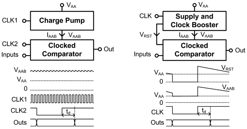
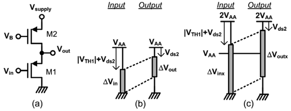
2. Supply Boosting Technique (SBT)

Supply boosting has not been investigated and used as extensively as the clock boosting or bootstrapping for designing low-voltage analog and mixed-signal circuits. One involving boosting supply voltage, is called charge-pump technique (CPT) used for designing OPAMPs, comparators, and phase-locked loops (PLLs) [912]. In the CPT, supply voltage is pumped continuously to keep circuit supply voltage (VAAB) higher than the system supply voltage (VAA) as shown on Figure 1a. Two clock signals are used in charge pump based circuits. The faster one is used by the charge pump block for maintaining low ripple on boosted supply voltage. The slower one is used by the main circuit which is a clocked comparator in this case.
Main benefits of using boosted supply voltage are extended input range and reduced system supply voltage. Low ripple voltage on the boosted supply voltage is required for CPT based circuits [9]. Otherwise it degrades noise performance of the main circuit. To achieve low ripple, sophisticated charge pump circuits have to be used which increase circuit complexity, size, and power consumption. Another important design requirement is that the boosted supply voltage has to be less than the maximum allowed process supply voltage (VAAP) for reliable device operation due to increased internal electric field. This is one of the main issues using boosting techniques in sub-100 nm processes in which VAAP is already around 1 V.
A modified version of the charge pump circuit design technique is proposed and called supply boosting technique (SBT) [1315]. In supply boosted circuits, system supply voltage is boosted locally only once allowing boosted voltages such as clock and supply voltages to drop from their boosted level, VAAB, as shown in Figure 1b. Sophisticated charge pump circuit used in CPT is replaced with a simple supply and clock booster (SCB) circuit. The SCB reduces circuit complexity, size, and overall noise performance of the main circuit. For clocked comparator, for example, one clock signal (CLK) is required resulting in a simplified clocking scheme. Also, a lower boosted supply voltage is chosen than the maximum allowed process supply voltage to avoid device reliability issues. Boosting supply voltage once also minimizes overall power consumption increased due to the added charge pump circuits. Thus, supply boosting technique based circuits achieve better energy efficiency than charge pump based circuits.
In the supply boosting circuit, supply voltage drops from the boosted level depending on the total current or power consumption of the main circuit. The higher the power consumption, the faster the supply voltage drops in supply boosted circuits. In this case, a larger supply voltage ripple is observed in charge pump based circuits. Large boosting or pump capacitors or lower current consumption is required for lower supply voltage drop or ripple. Increased capacitor size further increases dynamic power consumption of charge pump based circuits, while having a minimal effect on supply boosted circuits. Thus, a tradeoff among power consumption, speed, noise, and circuit size exists in both design techniques.

3. Supply Boosted Comparator (SBC) Design

The proposed supply boosted comparator (SBC) can be partitioned into sub blocks shown in Figure 2. It is composed of supply boosted level shifters (SBLS), latched comparator cores, buffers, and supply and clock booster (SCB) circuits. Boosted supply voltage (VAAB) and boosted clock signal (VRST) are generated by the compact supply and clock booster circuit. Boosted supply voltage is used by the p-type level shifter and first latched comparator, while boosted reset signal is used by pre-charge switches in latched comparators.

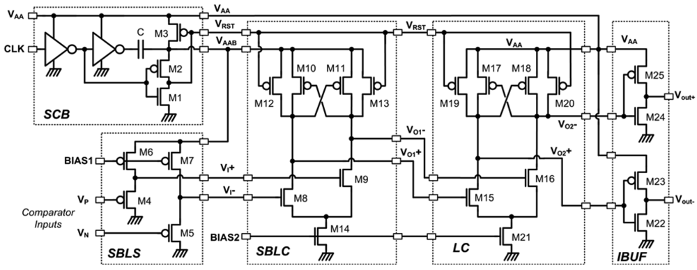
3.1. Supply and Clock Booster (SCB) Circuit

The supply and clock booster (SCB) circuit is composed of five transistors and a boosting capacitor as shown in Figure 2. It generates boosted supply and reset signal employing a one-shot charge pump circuit [16]. Boosted supply voltage (VAAB) equals the system supply voltage (VAA) when clock input is low (CLK = 0), and is ideally boosted to twice the system supply voltage (2VAA) when clock input is high.
The boosted reset signal (VRST) is 0 when clock input is low and boosted ideally to twice the system supply voltage (2VAA) when clock input is high. Bottom plate of the boosting capacitor (C) is connected to inverter side to improve boosting efficiency. Bulk nodes of PMOS devices in SCB (M2, M3) were connected to boosted supply output (VAAB). Boosting capacitor value can be calculated using (1).
C = t d × I AAB ( 1 α ) × V AAB
where td is comparator's delay time, α is discharge ratio of boosted supply voltage from its boosted level when clock input is high, and IAAB is total current consumption of the comparator circuits draining current from IAAB bus.
Ideal boosted level of the supply is 2VAA for the SCB circuit shown in Figure 2. Considering parasitic and the load capacitance (CL) on the SCB output, VAAB can be found using (2).
V AAB = ( 1 α ) × ( 2 C + C L C + C L ) × V A A = β V A A
where β is boosting factor. Required capacitor size for 10% drop on the boosted level (α = 0.1), 200 K conversions per second comparator speed (td = 5 μs), and 1 μW static power consumption (IAAB = 1 μA) on 1 V system supply voltage is 25 pF which could be integrated on-chip. Lowering current consumption will further reduce capacitor size. However, lowering current also results in larger comparator delay.

3.2. Supply Boosted Level Shifter (SBLS) Circuit

The supply boosted level shifter circuit is composed of p-type source followers driving and isolating input nodes from supply boosted comparator core. It expands common mode input range of comparator beyond the system supply voltage (VAAB) as shown in Figure 3. This expansion is achieved by using VAAB as the supply voltage for the level shifter during comparison period. Common mode input and output ranges of SBLS for supply voltage equal to VAAB and βVAA are given using (3) and (4).
Δ V i n = V A A | V T H 1 | V d s 2 Δ V out = G SPLS Δ V i n } for V supply = V A A
Δ V inx = β V A A | V T H 1 | V d s 2 Δ V outx = G SPLS Δ V inx } for V supply = β V A A
where GSPLS is small-signal voltage gain of the source follower. Here strong inversion is assumed for all transistors. Equations (3) and (4) are depicted for β = 2 on Figure 3b,c.
Common mode input range of the p-type source follower without supply boosting for 1 V system supply voltage is between 0.1 V and 0.6 V for PMOS threshold voltages between −0.9 V and −0.4 V. Supply boosting with β = 1.65 improves input range from 0.1 V to 0.75 V and from 0.6 V to 1.25 V for same threshold voltages. If the threshold voltage is less than −0.65 V, rail-to-rail input range could be achieved for 1 V supply voltage. Bulk node of input transistor (M1) has to be connected to the output to reduce signal dependent threshold variations and offset. Considering GSPLS of 0.8 and β = 1.65, output voltage swing can be increased from 0.08 V to 0.6 V for −0.9 V threshold voltage.

3.3. Latched Comparator (LC)

Comparator core composes a biased differential amplifier with regenerative type cross-coupled load functioning as latch. This continuous time latched comparator (LC) [17] provides lower kick-back noise and slower speed than its dynamic counterparts [18]. It works in two phases: pre-charge and compare. In pre-charge phase (VRST = 0) output nodes are connected to the boosted supply bus through PMOS switch transistors. In compare phase (VRST = VAAB), the switches are turned off and comparison of the input voltages is performed.
Since the differential pair is continuously biased, static power is consumed during both pre-charge and compare phases. Comparator cores are biased with tens of nA so that static power consumption is low. Low bias currents also allow one-shot supply boosting to be used more effectively.
N-type differential pair was used due to the fact that the differential input signals are level shifted by two p-type SBLS. The first latched comparator (SBLC) uses boosted supply voltage, VAAB, instead of the system supply voltage, VAA. Output of SBLC is coupled directly with the second latched comparator (LC). Supply voltage of the second LC is not boosted so that the logic level is restored before being driven by the inverter buffers which have high switching thresholds.

3.4. SBC Design and Simulation

The proposed supply boosted comparator shown in Figure 2 was designed using a 0.5 μm 2P3M CMOS process to achieve 10-bit resolution while attaining wide input common mode range. Threshold voltages of MOSFETs (+0.8 V/−0.9 V) in selected processes resulting in less than 0.1 V common mode input range for 1.0 V supply if a conventional clocked comparator is used. In the proposed comparator, the calculated common mode input range was 0.7 V, for β = 1.6 and GSPLS = 0.8.
Although supply boosting technique improves dynamic range of the comparator, it should be designed carefully according to speed limitations. Regeneration time constant of latched comparator core can be found using (5).
t d = C L g m , p = C L 2 K p ' ( W L ) p I D
where gm,p is the transconductance of cross coupled PMOS devices (M10, M11 or M17, M18 in Figure 2) and ID is their bias current. To reduce the regeneration time constant, gm,p must be increased by increasing its bias current. On the other hand, increasing the bias current causes the boosted supply voltage to drop at a higher rate and may cause failure unless the boosting capacitor is large enough. Since the size of the on-chip boosting capacitor cannot exceed a certain range due to limited area, proposed supply boosted comparator could only be used for low power, medium speed applications. For example, consider the SBC design supplied from a single 1 V power supply. For reliable operation of the comparator, the boosted supply must not fall below a certain level given in (6).
V AAB = | V THP | + 3 V o d
where Vod is the overdrive voltage of devices and VAAB can be found from (2). In (6), it is assumed that all devices have the same overdrive voltages. Hence the voltage drop (ΔV) across the boosting capacitor during the compare phase must not fall below a certain level that is given in (7)
Δ V < V AAB | V THP | 3 V o d
Since the comparison phase takes at least one time constant of the comparator, td, during this time we can write,
I AAB t d C < V AAB | V T P | 3 V o d
Using (5) in (8) and defining γ as the ratio of current in the latched comparator cores to the total comparator current, the maximum current that can be drained from the boosted supply can be found using (9). This gives the upper limit of the total current for a given boosting capacitor.
I AAB < 2 γ μ p C o x ( W L ) p ( C C L ) 2 ( V AAB | V T P | 3 V o d ) 2
Based on aforementioned considerations, a supply boosted comparator was designed in a 0.5 μm CMOS process. Device sizes used in the design are listed in Table 1. Long channel lengths were used to reduce input referred offset voltage, increase gain, and improve matching. 10 nA and 20 nA bias currents were used in SBLS and LCs, respectively. A 20 pF booster capacitor was used based on total static current of less than 100 nA and comparator delay of 50 μs for 1 V supply. Parasitic load capacitance of the SCB was around 4 pF resulting in α of 0.2 and β of 1.6.
Operation of proposed comparator was verified through HSpice simulation at different process, supply voltage and temperature (PVT) corners. Simulation result for 1.2 V supply, 1.0 V common mode input, and ±0.25 mV delta input voltage is shown in Figure 4. Comparator delay is mainly determined by second LC and switching threshold of the output buffer. Simulation shows two input cases: dVIN = +0.25 mV that force Vo+ to high between 20 μs and 30 μs, and dVIN = −0.25 mV forcing output lower, between 35 μs and 45 μs. Pre-charge time was 5 μs for the simulation. The delay introduced by the SBLS and SBLC for the first input is around 2.5 μs (Vo1− and Vo1+). Second LC and inverting buffer delay on the other hand is around 6 μs. Thus, there is room for improvement for a faster operation if a different second LC stage is used. One possible solution is using NMOS type SBLS following SBLC for improving conversion speed.
Layout size of the supply boosted comparator was 240 μm × 200 μm using SCMOS design rules (Lmin = 0.6 μm for C5) from MOSIS [19]. A 20 pF poly1-poly2 capacitor (0.8 fF/μm2) was used in the supply and clock booster block resulting in a boosting capacitor occupying almost 50% of the layout area. Micrograph of the SBC is shown in Figure 5.

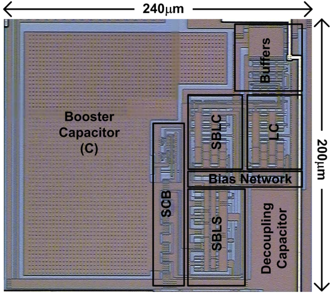
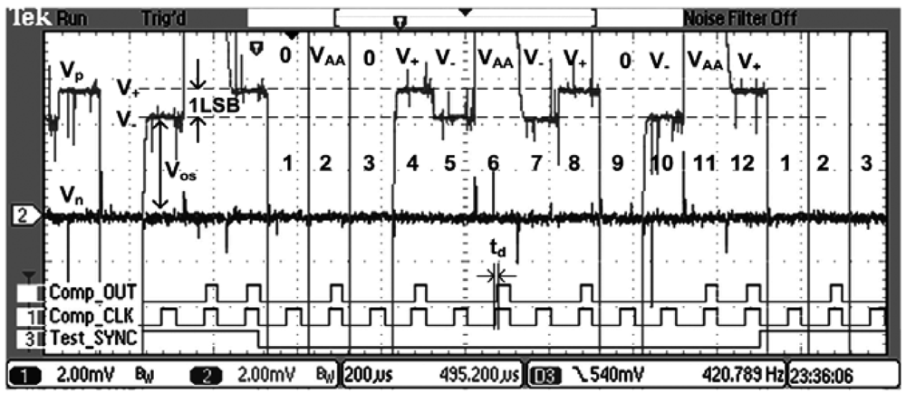
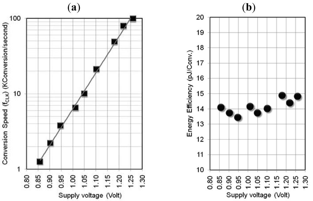
4. Measurement Results and Discussion

A test setup shown in Figure 6 was developed for measuring static and dynamic characteristics of the supply boosted comparator (SBC). Two 16-bit digital-to-analog converter (DAC) IC was used to generate SBC inputs. Control and communication signals were generated using a field programmable gate array (FPGA) on test board. Control signals in the design were level shifted from 3.3 V to desired system supply voltage (VAA) level. Analog and digital signals were monitored using mixed-signal oscilloscope (MSO) while current consumption was recorded through a precision multimeter (Tektronix DMM4050) with up to 0.1 nA resolution. Power supply to the SBC was separated from the other parts of the chip. Biases were generated on-chip and controlled digitally through a serial communication link.

Measurement Results

Power consumption and comparator delays were measured under worst-case input conditions described in [20]. A test pattern shown on Figure 7 was generated that is composed of 12 input transitions. They were generated by the 16-bit DACs and applied to positive and negative (Vp and Vn) inputs of the design. Four distinct voltage levels were generated as test patterns: VAA, 0, V+ and V. V equals the common mode voltage (VCMI) plus input offset voltage (VOS) of the comparator while V+ is kept one desired least significant bit (LSB) above the V level. Comparator's negative input (Vn) was kept at VCMI level while the test pattern was applied to positive input (Vp). Comparator delay time (td) was measured for worst case input transition. Transitions between levels 4 and 5 and levels 7 and 8 shown in Figure 7 are the worst case transitions that force comparator to resolve one LSB equivalent effective voltage difference applied to its inputs. Figure 7 also shows measured characteristics of SBC for VAA = 1.0 V and VCMI = 0.5 V. Measured 1LSB equivalent effective input voltage was 1.2 mV, and offset voltage was 4.1 mV.
Delay time (td) versus average power consumption (Pavr) of the comparator was measured at various biasing conditions. Delta input voltage (dV = V+V) was 1 mV, while clock frequency (fCLK) was set to 4 kHz with duty cycle of 20% during this measurement. Dynamic power consumption was measured by setting comparator's bias currents to zero while running the clock. It was 25 nW. Measurement results are shown in Figure 8. It represents the tradeoff between speed and power consumption of SBC.
Delay time, maximum clock speed, and power consumption of the SBC were also measured for VAA between 0.85 V and 1.25 V. dV = 5 mV and VCMI = VAA/2 was used during measurements. Figure 9a shows the measured maximum clock frequency versus supply voltage while Figure 9b represents calculated energy efficiency of the SBC. Energy efficiency was calculated using (10) using measured power consumption and maximum conversion speed of the comparator.
E eff . [ Joule / Conversion ] = Power [ Watt ] Speed [ Conversion / Second ]
Measured energy efficiency was fairly constant and was between 13 and 15 pJ per conversion. Measured minimum supply voltage of the SBC design was 0.85 V with better than 1000 conversions per second speed.
Precision of the comparator (VPRCS) was measured for supply voltages between 0.85 V and 1.2 V while sweeping common mode input voltage (VCMI) between 0 and VAA as shown in Figure 10. Bit resolution of the SBC was then calculated using (11) and plotted in Figure 11.
n = 3.32 log 10 ( V CMI / V PRCS )
For 8-bit resolution common mode, input range was measured to be around 60% of the system supply voltage, while it was about 55% and 40% for 9-bit and 10-bit resolutions, respectively. Compared to conventional comparators, this represents six times (6×) improvement of the common mode input range for 8-bit resolution when VAA = 1 V.
Measurement results of the supply boosted comparator at 1.0 V supply voltage are summarized and compared in Table-2. The SBC achieves lower supply voltage operation, better power consumption and energy efficiency, without increasing complexity and area of the comparator.

5. Conclusion

A new comparator topology was proposed utilizing the supply boosting technique (SBT) to achieve sub-1V operation. It was shown that SBT improves the common mode input range of the comparator, achieving both high precision and low energy operation. The proposed comparator topology would be especially useful in mixed-signal systems such as implantable biomedical devices that use CMOS process for which only high-VTH MOSFET devices are available.
The proposed comparator was fabricated using a 0.5 μm CMOS process. Measurements showed that the comparator achieved better than 15 pJ/conversion energy efficiency, 0.62 V common mode input range which is six times better than that of conventional comparator topologies with 8-bit resolution on a 1 V supply.
The speed of the supply boosted comparator is mainly determined by the second latched comparator stage. Speed could be improved using an N type source follower following first supply boosted latch comparator (SBLC) circuit. It is expected that this improvement would be between six and ten times the current speed for 8-bit resolution.
Figure 1. Characteristic signals and blocks of a clocked comparator using: (a) charge pump technique (CPT); (b) supply boosting technique (SBT).
Jlpea 01 00247f1
Figure 2. Schematic diagram of proposed supply boosted comparator (SBC).
Jlpea 01 00247f2
Figure 3. Supply boosted level shifter (SBLS) circuit; (a) schematic; (b) common mode input and output ranges for Vsupply = VAA; (c) for Vsupply = 2VAA.
Jlpea 01 00247f3
Figure 4. Hspice simulation result of the supply boosted comparator for VAA = 1.2 V, VIN,DC = 1.0 V, dVIN = ±0.25 mV.
Jlpea 01 00247f4
Figure 5. Micrograph of the SBC design.
Jlpea 01 00247f5
Figure 6. Measurement setup.
Jlpea 01 00247f6
Figure 7. Input and output signals captured during dynamic testing of supply boosted comparator under worst case input conditions.
Jlpea 01 00247f7
Figure 8. Measured power consumption versus comparator delay for VAA = 1.0 V, Vn = 0.5 V, dV = +1 mV, fCLK = 4 kHz.
Jlpea 01 00247f8
Figure 9. Measured: (a) conversion speed and (b) energy efficiency of SBC.
Jlpea 01 00247f9
Figure 10. Measured precision of the SBC for various supply voltages.
Jlpea 01 00247f10
Figure 11. Measured bit resolution of the SBC for various supply voltages.
Jlpea 01 00247f11
Table 1. Device sizes used in SBC design.
DeviceWidth (μm)Length (μm)M
M16.00.62
M2–36.00.64
M4–5,10–11,17–186.01.28
M6–7,14,216.03.02
M8–9,15–166.01.58
M23,256.00.98
M22,246.01.24
M12–13,19–206.00.61
Table 2. Comparison table.
Parametersthis WorkRef. [20]Ref. [5]Unit
CMOS Process Technology0.500.500.25μm
tdreshold voltage (N/P)+0.8/−0.9+0.74/−0.85+0.48/−0.6Volt
Supply Voltage1.01.01.0Volt
Supply Voltage Range>0.85>1.0>1.0Volt
Input Range (VCMI)0.751.01.0Volt
Conversion Speed6.52501000 aKC/s
Power Consumption0.095.021.0μWatt
Energy Efficiency14.020.021.0pJ/C
Layout Area (LA)0.0480.0370.024mm2
Normalized Area b133,300 c147,200384,000-
asimulation only;
bLA/Lmin2;
cLmin = 0.6 μm.

Acknowledgments

This research was supported partially by Micron Technology Foundation.

References

  1. Bechen, B.; Boom, T.V.D.; Weiler, D.; Hosticka, B.J. Theoretical and Practical Minimum of the Power Consumption of 3 ADCs in SC Technique. Proceedings of the 18th European Conference on Circuit Theory and Design, Sevilla, Spain, 27–30 August 2007; pp. 444–447.
  2. Wang, A.; Calhoun, B.H.; Chandrakasan, A.P. Sub-Threshold Design for Ultra Low-Power Systems; Springer: New York, NY, USA, 2006. [Google Scholar]
  3. Chang, L.; Frank, D.J.; Montoye, R.K.; Koester, S.J.; Ji, B.J.; Coteus, P.W.; Dennard, R.H.; Haensch, W. Practical strategies for power-efficient computing technologies. Proc. IEEE 2010, 98, 215–236. [Google Scholar]
  4. Hung, Y.C.; Liu, B.D. A low-voltage wide-input CMOS comparator for sensor application using back-gate technique. Biosens. Bioelectron. 2004, 20, 53–59. [Google Scholar]
  5. Baschirotto, A.; Castello, R. A 1-V 1.8-MHz CMOS switched-opamp SC filter with rail-to-rail output swing. IEEE J. Solid-State Circuits 1997, 32, 1979–1986. [Google Scholar]
  6. Huang, C.J.; Huang, H.Y. A Low-Voltage CMOS Rail-to Rail Operational Amplifier Using Double P-Channel Differential Input Pairs. Proceedings of the 2004 IEEE International Symposium on Circuits and Systems (ISCAS), Vancouver, Canada, 23–26 May 2004; 1, pp. 673–676.
  7. Abo, A.; Gray, P. A 1.5-V, 10-bit, 14-MS/s CMOS pipeline analog-to-digital converter. IEEE J. Solid-State Circuits 1999, 34, 599–606. [Google Scholar]
  8. Mortezapour, S.; Lee, E.K.F. A 1-V 8-bit successive approximation ADC in standard CMOS process. IEEE J. Solid-State Circuits 2000, 35, 642–646. [Google Scholar]
  9. Duisters, T.A.F.; Dijkmans, E.C. A-90-dB THD rail-to-rail input OPAMP using a new local charge pump in CMOS. IEEE J. Solid-State Circuits 1998, 33, 947–955. [Google Scholar]
  10. Pierre, R.S. Low-power BiCMOS op amp with integrated current mode charge pump. IEEE J. Solid State Circuits 2000, 35, 1046–1050. [Google Scholar]
  11. Lotfi, R.; Taherzadeh-Sani, M.; Azizi, M.Y.; Shoaei, O. A 1-V MOSFET-Only Fully-Differential Dynamic Comparator for Use in Low-Voltage Pipelined A/D Converters. Proceedings of the 2003 International Symposium on Signals, Circuits and Systems (SCS), Lasi, Romania, 10–11 July 2003; 2, pp. 377–380.
  12. Lee, S.C.; Park, D.S.; Song, J.H.; Choi, M.W.; Lee, S.H. A Low-Ripple Switched-Capacitor DC-DC up Converter for Low-Voltage Applications. Proceedings of the Second IEEE Asia Pacific Conference on ASICs, Cheju, South Korea, 28–30 August 2000; pp. 13–16.
  13. Mesgarani, A.; Alam, M.N.; Nelson, F.Z.; Ay, S.U. Supply Boosting Technique for Designing Very Low-Voltage Mixed-Signal Circuits in Standard CMOS. Proceedings of the 2010 IEEE Midwest Symposium on Circuits and Systems (MWSCAS), Seattle, WA, USA, 1–4 August 2010; pp. 893–896.
  14. Ay, S.U. A sub-1Volt 10-bit Supply Boosted SAR ADC Design in Standard CMOS. Int. J. Analog Integr. Circuits Signal Process. 2010, 66, 213–221. [Google Scholar]
  15. Ay, S.U. A 1.32 pW/frame pixel 1.2 V CMOS Energy Harvesting and Imaging (EHI) APS Imager. Proceedings of the 2011 IEEE International Solid- State Circuits Conference, San Francisco, CA, USA, 20–24 February 2011; pp. 116–117.
  16. Senderowicz, D.; Nicollini, G.; Pernici, S.; Nagari, A.; Confalonieri, P.; Davalle, C. Low-Voltage Double-Sampled ΣΔ Converters Applications. Proceedings of the 1997 IEEE International Solid- State Circuits Conference, San Francisco, CA, USA, 6–8 February 1997; pp. 210–211.
  17. Figueiredo, P.M.; Vital, J.C. Kickback noise reduction techniques for CMOS latched comparators. IEEE Trans. Circuits Syst. II 2006, 53, 541–545. [Google Scholar]
  18. Cho, T.; Gray, P. A 10 b, 20 M sample/s, 35 mW pipeline A/D converter. IEEE J. Solid-State Circuits 1995, 30, 166–172. [Google Scholar]
  19. MOSIS Homepage. Available online: http://www.mosis.com (accessed on 23 June 2011).
  20. Fayomi, C.J.B.; Roberts, G.W.; Sawan, M. Low Power/Low Voltage High Speed CMOS Differential Track and Latch Comparator with Rail-to-Rail Input. Proceedings of the 2000 IEEE International Symposium on Circuits and Systems, Geneva, Switzerland, 28–31 May 2000; 5, pp. 653–656.

