1. Introduction
By examining modern smart portable devices, one can find plenty of voltage domains which intended to serve different modules and sub-modules inside those devices [
1,
2]. The straightforward way to serve all these modules and sub-modules is to have a dedicated voltage converter/regulator from the main battery to each one of them. This is not an optimal design, since it would require each converter to have its external passive components and controller in addition to mitigating the EMI among the different inductors. Multi-output converters are therefore becoming very popular in modern devices. These converters may be of linear, switching, step-down, or step-up type with digital or analog voltage or current control. There are different ways these outputs can be related to each other and controlled [
3]. The most versatile form is a multi-output model that can serve different loads independently, along with common control parts to ensure compactness, higher efficiency, and re-use of the resources.
The WLED driver ideally operates in a similar manner to a voltage-regulated boost converter, except it regulates the output current through the string of LEDs with high power efficiency, especially in portable devices. Besides, there is a need for an accurate current within any string and among the different strings to guarantee consistency in brightness [
4]. A multi-string WLED driver is a natural application of multi-independent-output converters. The traditional architecture of multi-string WLED drivers has all strings connected to the same output node, which is
, as shown in
Figure 1. Despite its simple architecture with a common controller, single OVP circuitry, and a minimum number of switches per string [
5,
6,
7,
8], it suffers from lower power efficiency and current mismatching among strings. This is particularly true in an asymmetrical string arrangement and low process nodes, such as a 40 nm process node. Even with a symmetrical string arrangement, white LEDs typically have different forward voltage (
) drops. Practically, the value of
varies between 2 and 4 V, even if these WLEDs come from the same batch at the manufacturing facility. Additionally, the
drop in each of these WLEDs is a function of temperature [
9,
10,
11]. Therefore, a multi-string driver with the same number of WLEDs per string may require different voltages to satisfy all WLEDs in the string plus the current sink overhead.
To overcome the disadvantages above of the typical architecture, multiple independent output WLED drivers are becoming the mainstream topology [
12,
13]. However, this comes with a potentially higher number of switches per string, more complex control circuitry, and multiple circuits (one per output) for common features such as over-voltage protection (OVP).
This work proposes a single-inductor, multiple-independent-output, multi-string architecture using a 40 nm CMOS process node. Using a single inductor, a minimum number of switches per string, and a simple and common controller, excellent current matching among strings is achieved. This solution requires a single OVP circuit for all independent outputs. Furthermore, the proposed solution has high power efficiency, almost all-digital design methodology, easy digital dimming, and expandable design when increasing the number of strings. The rest of the paper is organized as follows:
Section 2 discusses the basic operational principles of the proposed architecture, including a performance evaluation.
Section 3 describes the individual circuits comprising the proposed architecture.
Section 4 summarizes the simulation setups and results. Finally, conclusions are covered in
Section 5.
2. Proposed Architecture, Basic Operational Principles, and Performance Evaluation
The proposed architecture and its basic operation are described in
Section 2.1.
Section 2.2 presents the most popular published current drivers.
2.1. The Proposed Architecture and Its Basic Operation
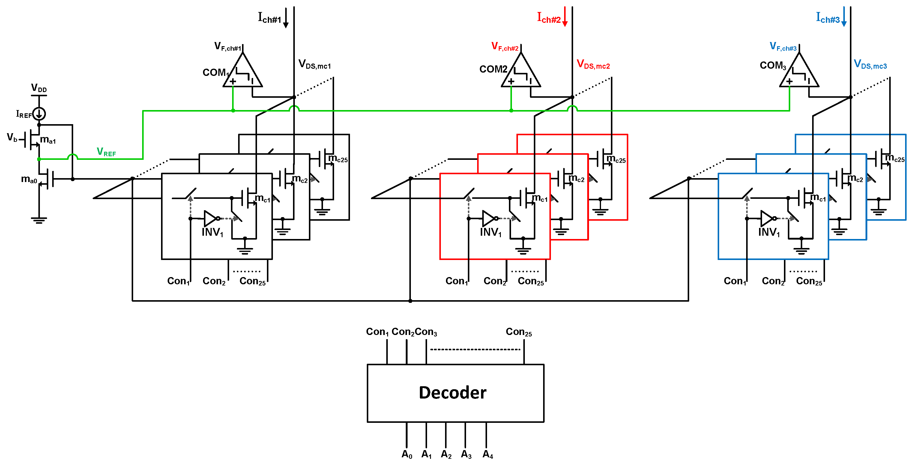
Figure 2 shows the overall block diagram of the proposed architecture. This WLED driver is based on a boost converter with a single common inductor (
); a common main switch (
); a high-side switch; an output capacitor for each independent output (string); a current matching circuit; and a maximum duty cycle controller (MDCC) that consists of a forward voltage compensation circuit, a charge pump, a PWM block to control, and a drive for the main switch. A simple pulse skipping controller (PSC) is used to control the gates of the high-side switches. For optimal power efficiency of 18 WLEDs, typically enough for a smartphone backlight, WLEDs are arranged as three strings; each has 6 WLEDs [
4].
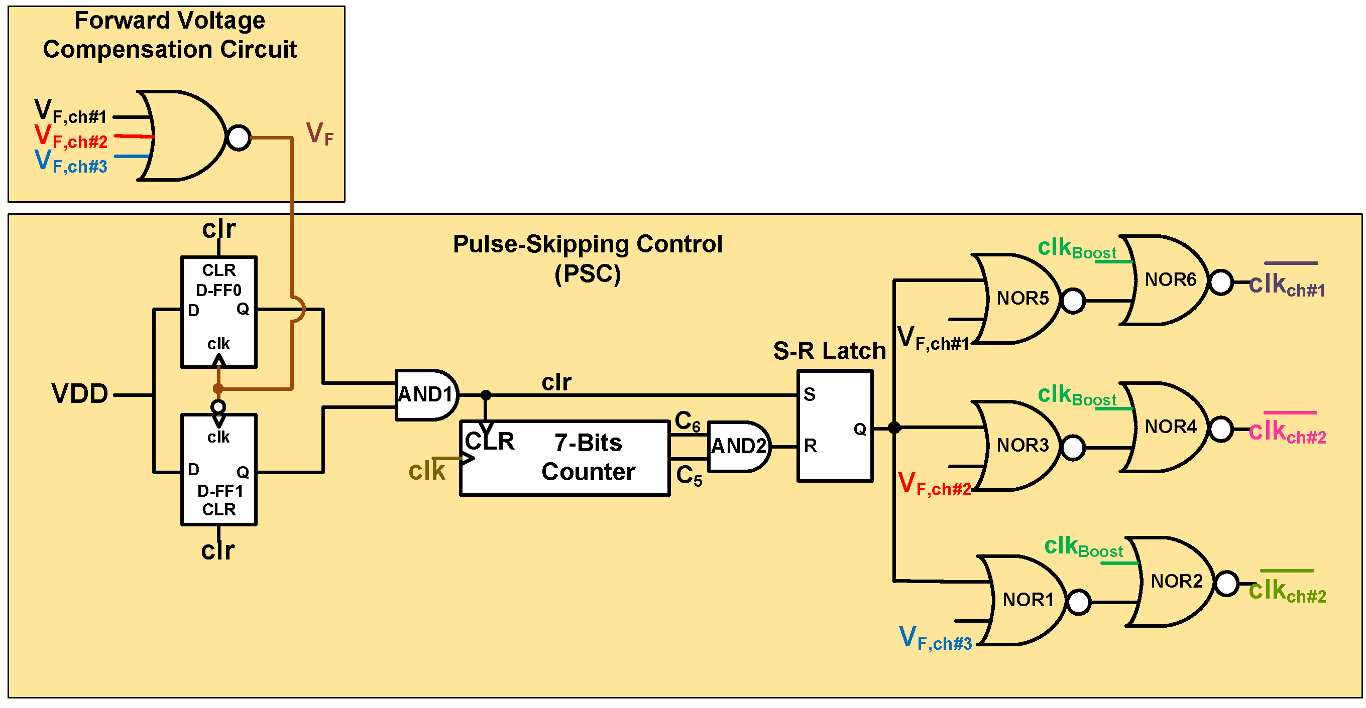
There are two modes of operation: MDCC mode and PSC mode. In the MDCC mode of operation, the MDCC controller produces the signal that drives the main switch to the maximum duty cycle () needed for all strings to be conductive. In this mode, the main switch is driven by duty cycle D and high-side switches are driven by 1D. Arriving at suggests that all strings have reached the targeted current . At that moment, the PSC mode of operation starts pulse-skipping on the individual high-side switches to get rid of any extra voltage/current accumulated during the initial startup procedure (prior to reaching ). A constant value of zero for the signal indicates the MDCC mode of operation; a pulsating value indicates the pulse-skipping mode. If any of the strings’ current sinks’ overheads drops below the reference voltage (), which is equivalent to , back to zero, the MDCC mode starts again and this continues forever.
Figure 3 illustrates the timing of the different gate pulse drivers for the main and high-side switches. It shows how the PSC starts pulse skipping mode on the high-side switches once the
has been reached at the main switch using MDCC. These waveforms reflect a scenario where the total voltage drop of WLEDs (
) in string 1 is the lowest and that in string 3 is the highest.
If an open circuit condition has been detected, the OVP indicator stops switching, and the system starts all over again at the beginning of the next cycle. In the case of any WLED short-circuit, the system keeps working as if nothing has happened. This is true since the system is designed to work with unbalanced strings, so it acts as if that string is one WLED less in the count.
2.2. Current Matching
In this subsection, the most popular published art current drivers are investigated, along with their shortcomings. The proposed current driver, along with its advantages over published art, is expanded in the following section.
There exists more than one design for regulated current sinks placed in series with the WLEDs in each string [
12,
13].
Figure 4 depicts two possibilities.
Figure 4a shows a regulated current sink using a high gain amplifier, a pass transistor, and an external resistor. In this case, the current that passes through each string of WLEDs would be
. Adding a resistor would cause efficiency degradation due to a power loss of
. The parasitic resistance of the pin should also be estimated and included in the calculations to have more accurate current values. To overcome the parasitic effect,
needs to be large which causes more power dissipation. On the other hand, if the resistor is integrated into the same IC, it would have large tolerance due to the process and temperature variation, which may lead to error in the driving current and consequently change in the color brightness.
Figure 4b shows a cascode mirror with an amplifier forcing both drain-to-source voltages to be equal without using resistive elements. However, the current ratio between the reference current (
A) and the WLED current (25 mA) is 250×. This big ratio degrades the current accuracy. The result could be worse than using the resistor due to the mismatch between the two transistors and process variation. The overhead needed to operate the transistors in the saturation region may require around 200–300 mV for each transistor. That adds up to a voltage higher than the voltage across the resistor. This consequently degrades the power efficiency even more.
4. Simulation Results
The simulation was conducted with ADS CAD tools using 40 nm 1P9M TSMC CMOS technology. A standard 40 nm CMOS process has been used. In this process, the parasitic effects, including pad parasitic, were expected to have minimal effect as the selected switching frequency (1 MHz) was well below the unity-gain frequency (
GHz) [
15].
Figure 11 shows the three different independent output voltages generated based on the need to cover both WLEDs’ voltage drops and the current sink overhead of each string. Clearly, the magnitude of the output voltages is different in each string, as it is impossible to have exact voltages even if all strings are balanced (having the same number of WLEDs), as explained before.
Figure 12 shows the current sinks’ overhead voltages, one per string. Clearly, in the beginning, the overhead was higher than 250 mV, for the two strings with the lowest voltages needed to satisfy all WLEDs and their respective overhead current sinks. The lowest overhead voltage belonged to the highest voltage needed until
was reached. Once
reached the proper value, the higher overhead voltages started going down as the PSC mode started, until all overheads reached a steady-state value of around 250 mV.
Figure 13 shows the currents in each string. The steady-state value is equal to the targeted value of 25 mA in each string. Of course, the steady-state value can be 1 to 25 mA as per the decoder input, as explained before. The lowest voltages of the three strings show higher currents compared to the highest voltage string while searching for
in the MDCC mode of operation. Once the
has been reached, the higher current starts going down (PSC mode starts) and continues until it reaches a steady-state of the targeted value of 25 mA.
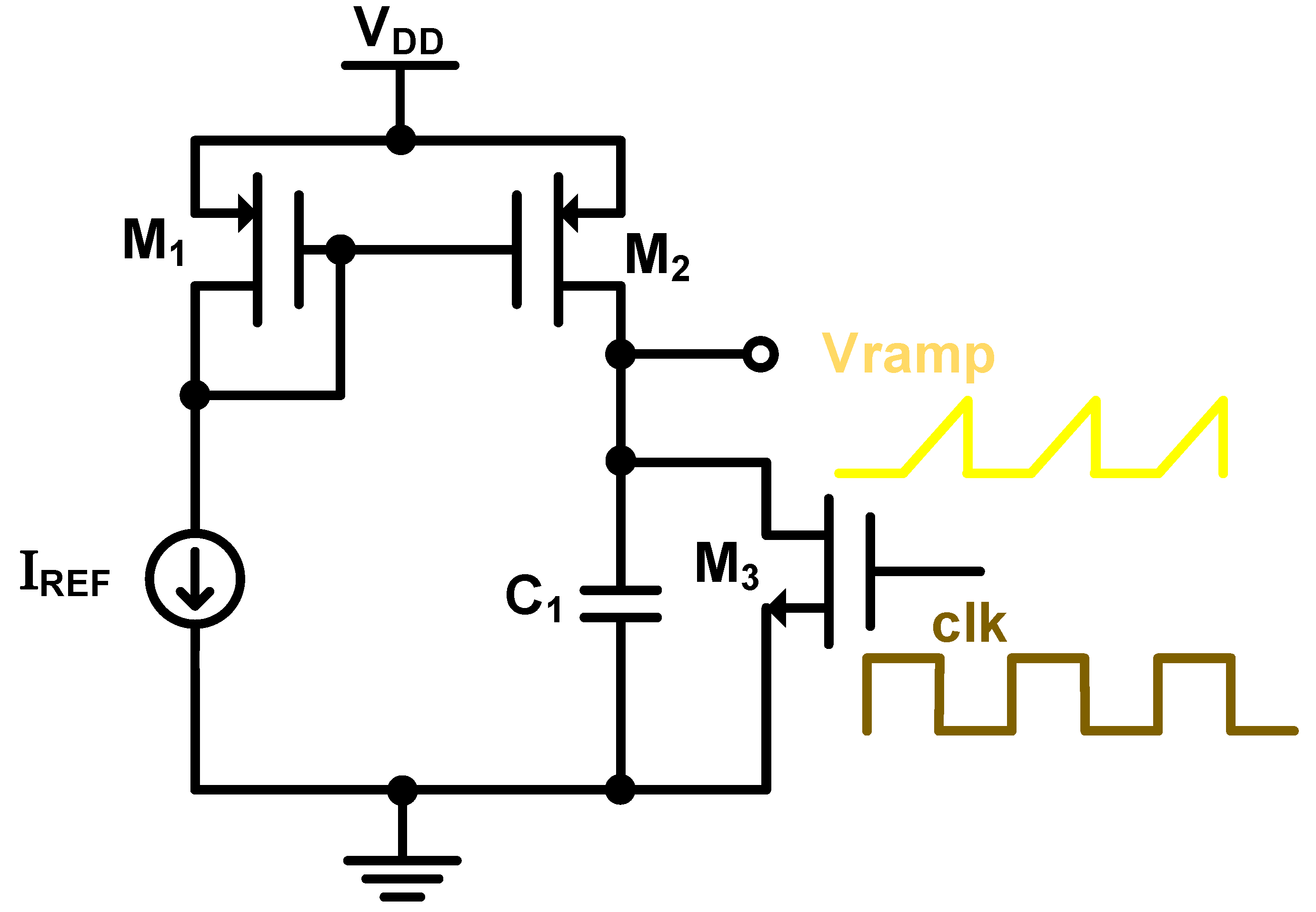
Figure 14 shows the control signal (
), the ramp signal (
), the duty cycle signal (
), and the clock signal (
). As mentioned before, the
signal stays high beyond the minimum 50% until the
becomes smaller than the
signal. Note that the
is only active when the
signal is low and its switching period is
s.
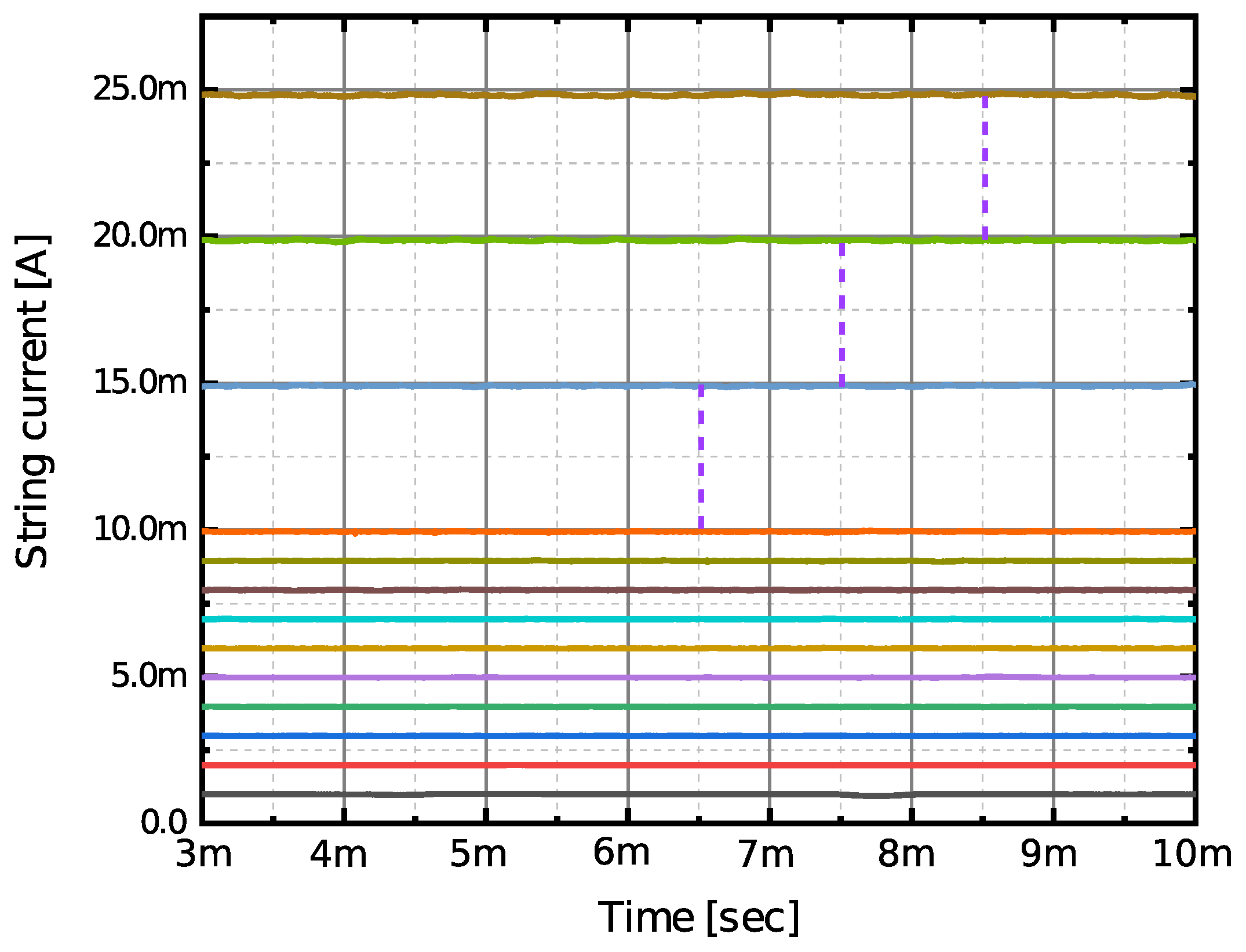
Figure 15 demonstrates the capability of setting the current value to any of the 25 possible options. Each segment carried 1 mA of current. The time simulation stepped up the current by 1 mA until we reached the 10 mA mark. After that, 5 mA steps were implemented until the 25 mA mark was reached.
Literature Feature Comparison
Table 1 shows a list of helpful and necessary features of the multi-output WLED drivers. A brief comparison is drawn amongst the different architectures and that of this work in terms of key features. It is clear from the table that the proposed architecture is the only one among all those shown that supports both modes of operation (CCM and DCM). With multiple independent outputs, most architectures require separate OVP circuits, one per output. The proposed architecture allows the usage of a single OVP circuit for all outputs. This is attainable because the used controller waits for the highest output to reach its final value (without exceeding the voltage limit) before enabling the pulse-skipping mode in which the other two outputs reach their lower final values.
Despite all the benefits of having a simple node, it has greater challenges in building current drivers due to smaller output (channel) resistance, , which is crucial in making highly accurate current sinks. This problem is taken care of in the proposed solution by using feedback controllers MDCC and PSC that force the same string WLED current via forcing the same over-drive voltage () of all current sinks. This way, the proposed architecture uses the most advanced node along with all its benefits, and remedies its most unwanted disadvantage. Many published architectures utilize multiple switches per independent output and clocks to pack different outputs within the zero-current period in the DCM model. This may demand timing synchronization, hence a need for accuracy or otherwise potential errors and malfunctioning. The proposed work does not use inter-dependent timing signals and hence does not need any synchronization among them. This leads to a more durable solution that can tolerate more imperfections in the manufacturing process, temperature, and supply voltage variations, in addition to any other limitations that may impose themselves, such as a maximum number of outputs (strings) that can be supported.
This naturally leads to the conclusion that this proposed circuit is the simplest among all listed architectures. Dimming and dimming resolution are easily adapted and implanted in the proposed architecture. Dimming accuracy or resolution can also be modified and improved in the proposed architecture. Switching frequency is the constant frequency used in the converter within the WLED driver. It is worthy to note that all integrated circuits reviewed in
Table 1 use a switching frequency around 1 MHz to help reduce the passive components’ size. Therefore, a switching frequency of 1 MHz clk is utilized in this work.
The input voltage range of the proposed architecture matches the most popular battery’s usable voltage range ( V to V). The output voltage depends on the number of WLEDs per string. Since a boost converter is used, a conversion ratio of no more than six is used to keep the system efficiency higher by running in CCM mode. A typical low-power WLED current is around 20 to 25 mA. This architecture supports current segmentation from 1 to 25 mA in each string. Efficiency is probably the most crucial metric in the WLED driver: since the output voltage is high, WLED currents are not small either. In all aspects of the design, power-savings and selection of ultra-low-power components are prioritized. A good example is the double-tail comparators used in the current matching circuit, where the comparator static power has a value of zero.
5. Conclusions
In this work, a multi-independent-output, multi-string, high-efficiency, boost-converter-based white LED (WLED) driver architecture was proposed. The feedback loop utilizes a single inductor main switch with a common maximum duty cycle controller (MDCC). A simple pulse skipping controller (PSC) is utilized in each high-side switch of the multiple independent outputs. An open circuit in any of the strings is also addressed in addition to any LED short circuit condition. Increasing the number of independent output strings can be done so long as the power stage is appropriately scaled. Although a three-string design is demonstrated, a lesser number of output strings (e.g., single-output) can be easily accommodated by merely disabling the relevant feedback signal (i.e.,) of the removed channel. In the proposed design, each string is driven by a 25 mA current sink. An input voltage of 3.2–4.2 V and an output voltage of up to 27 V are supported. Excellent current matching between strings is achieved, despite the low on-resistance of transistors used in the 40 nm process. Despite the presence of multiple independent outputs, a single over-voltage protection (OVP) circuit is used at the output to protect the circuit from any voltage above 27 V. The proposed design does not rely on time multiplexing; hence, it supports both modes of operation, CCM and DCM. A improvement in efficiency is achieved relative to extremely unbalanced strings. Future work will include fabrication with an on-chip oscillator to generate the 1 MHz clk in a 40 nm 1P9M TSMC CMOS node.


