Article

Understanding Timing Error Characteristics from Overclocked Systolic Multiply–Accumulate Arrays in FPGAs

Bridge Lab, Electrical and Computer Engineering, Utah State University, Logan, UT 84321, USA
*
Author to whom correspondence should be addressed.
J. Low Power Electron. Appl. 2024, 14(1), 4; https://doi.org/10.3390/jlpea14010004
Submission received: 15 September 2023 / Revised: 8 December 2023 / Accepted: 12 December 2023 / Published: 9 January 2024

Abstract

:
Artificial Intelligence (AI) hardware accelerators have seen tremendous developments in recent years due to the rapid growth of AI in multiple fields. Many such accelerators comprise a Systolic Multiply–Accumulate Array (SMA) as its computational brain. In this paper, we investigate the faulty output characterization of an SMA in a real silicon FPGA board. Experiments were run on a single Zybo Z7-20 board to control for process variation at nominal voltage and in small batches to control for temperature. The FPGA is rated up to 800 MHz in the data sheet due to the max frequency of the PLL, but the design is written using Verilog for the FPGA and C++ for the processor and synthesized with a chosen constraint of a 125 MHz clock. We then operate the system at a frequency range of 125 MHz to 450 MHz for the FPGA and the nominal 667 MHz for the processor core to produce timing errors in the FPGA without affecting the processor. Our extensive experimental platform with a hardware–software ecosystem provides a methodological pathway that reveals fascinating characteristics of SMA behavior under an overclocked environment. While one may intuitively expect that timing errors resulting from overclocked hardware may produce a wide variation in output values, our post-silicon evaluation reveals a lack of variation in erroneous output values. We found an intriguing pattern where error output values are stable for a given input across a range of operating frequencies far exceeding the rated frequency of the FPGA.

1. Introduction

Artificial Intelligence (AI) hardware accelerators have seen tremendous developments in recent years due to the rapid growth of AI in multiple fields, including image processing [1], medical diagnosis [2], and speech recognition [3], among others. Many of these accelerators contain a customized Systolic Multiply–Accumulate Array (SMA) as its computing brain, where most of the actual data manipulation takes place. Consequently, functionally correct execution through these SMAs dictates application-level execution quality, such as inference accuracy or training efficiency.
The operating frequency and supply voltage of these AI hardware accelerators have a major role in both their functional correctness and energy efficiency. Timing errors occur when the SMA is undervolted or overclocked to the point that the circuit is no longer able to complete its computation in time, resulting in wrong computational data. Broadly, there are two distinct methodologies used for studying timing errors or faults in digital circuits: simulation and hardware implementation. Simulation techniques have been used extensively in processors [4,5], GPUs [6], ASICs [7], as well as FPGAs [8]. Simulation techniques are software-intensive and often used to evaluate new ideas and architectures. On the other hand, hardware implementation techniques require substantial engineering efforts and are specific to vendors and devices. Hardware implementations in research are closer to integrated circuits that would be deployed in real-world scenarios when compared to software simulation techniques. Low-power hardware implementation works exist in CPUs [9], GPUs [10], ASICs [11], and memories [12,13]. However, to the best of our knowledge, timing errors have not been well investigated for DNN hardware accelerators based on FPGAs. There are several works that attempt to study undervolting in FPGAs [14,15] but use non-scalable ad hoc techniques to account for process variation effects. Our work takes a step toward addressing this critical gap.
In this paper, we look further into the faulty output characterization of a representative SMA building block in a real silicon overclocked environment. Specifically, the three major goals of this study are: (i) identify the nature of faulty output alteration from a standard SMA block for a holistic circuit–architectural understanding of the application-level error behavior; (ii) substantially improve SMA fault tolerant design by understanding how errors from overclocked hardware are far from a random distribution—a common assumption in a large body of software-based fault simulation works [16,17,18,19]; and (iii) use our extensive SMA timing error characterization to spawn a new class of predictive techniques to sustain application-level goals (e.g., high inference accuracy), while still operating at a lower voltage or higher clock speed. Many recent works that aim to predict timing errors in a processor or SMA pipeline are usually limited to speculating an error event rather than the erroneous output [20,21]. Our findings, as detailed next, can make significant progress in fault-tolerant hardware design by identifying certain properties of the erroneous outputs that have not been demonstrated before.
We make the following contributions in this paper:
  • We uncover fascinating error characteristics in an SMA building block implemented using an FPGA (Section 2). While intuitively, one may expect that timing errors resulting from overclocked hardware may produce a wide variation in output values, our integrated hardware–software experimental platform reveals a lack of variation in erroneous output values.
  • Based on our intriguing findings, we identify a set of four representative input patterns for an SMA building block. These four patterns are based on their distinct circuit-level activity through the SMA building block and are referred to as Identity Activation, Diagonal Activation, Hamming Activation, and Prime Activation (Section 3).
  • We establish a rigorous experimental platform using a software–hardware co-simulation and execution. Our results are obtained in a comprehensive FPGA environment, where an SMA building block is running a specific input pattern under a range of frequencies that rise beyond the rated frequency upper bound of execution of that block (Section 4).
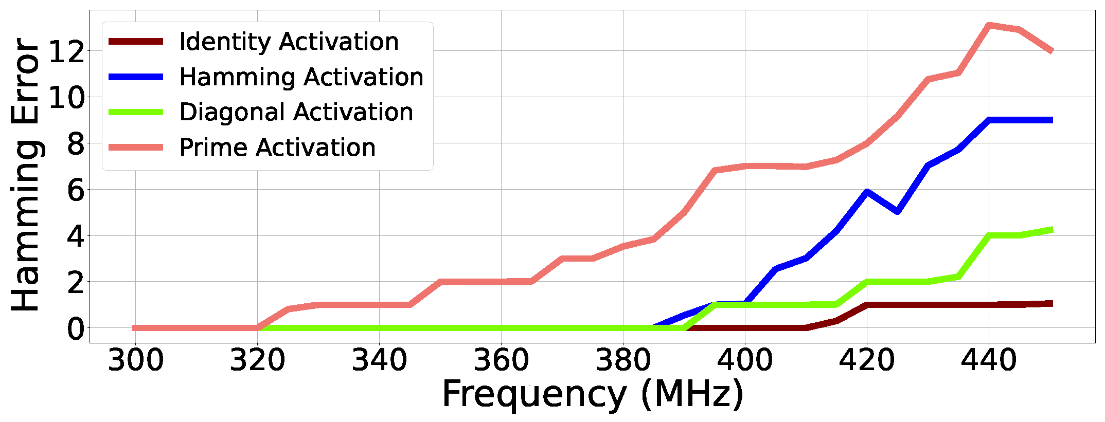
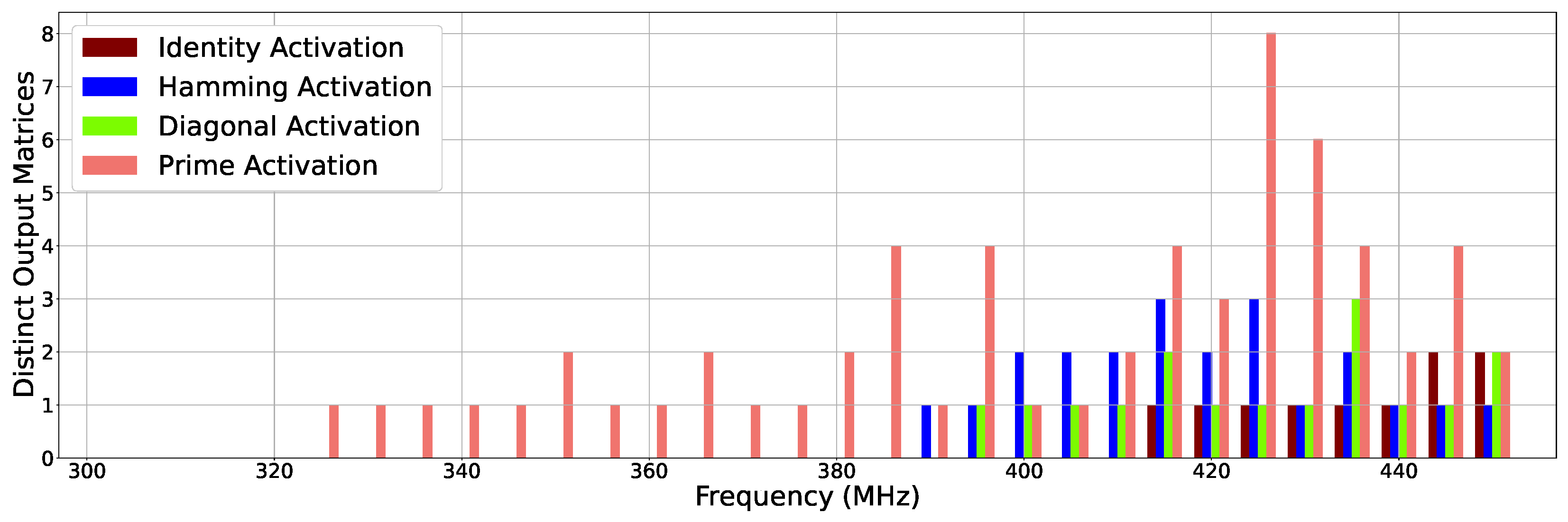
  • Our comprehensive experiments and analysis reveal several fascinating characteristics of erroneous outputs produced from the SMA building block under an overclocked environment (Section 5). First, we notice that the hamming distance between the correct output and erroneous output is often stable across input patterns and frequencies. Second, different input patterns show a variation in the total number of distinct erroneous output values seen. For example, Identity Activation shows at most two distinct erroneous output matrices, while Prime Activation shows up to eight different output values across a wide range of frequencies that vary between 1× and 3.5× relative to the rated frequency of the hardware design.
  • Our paper presents a methodological pathway to characterize an SMA block implemented in an FPGA platform. It is likely that a different board from the same vendor or competing vendor shows different timing error characteristics. However, we believe that our process of such characterization laid out in this work will still be applicable across various boards and vendors.

2. Motivation

In this section, we demonstrate a slew of fascinating error behaviors of a fundamental building block of an SMA under overclocked operating conditions. We begin by providing a short background of the dataflow through such a building block (Section 2.1) and our justification for overclocking (Section 2.2), followed by an outline of our experimental setup (Section 2.3). We discuss our empirical error data in Section 2.4 and conclude with the significance of our observation in Section 2.5.

2.1. Dataflow in an SMA Building Block

Figure 1 shows the cycle-by-cycle dataflow through a 2 × 2 SMA architecture. We can observe several key characteristics of this unique dataflow. First, we observe that activation vectors are streamed from the left to right MACs, while partial sums flow from the top to bottom MACs. Second, we notice that different MACs are active in different cycles. For example, MAC 1 is active in cycles one and two but inactive in the remaining cycles. Third, we notice that output elements from the entire building block appear at different cycles, similar to the sporadic activity seen in the MAC units. For example, o u t p u t 1 appears in cycle 2 while o u t p u t 4 appears in cycle 4. Recognizing this particular temporal sequence of output elements is critical for an accurate analysis of data in our experiments, as described in Section 2.3.

2.2. Why Overclocking Is Chosen for This Work

Any hardware logic circuit block is designed to perform at a rated voltage and frequency range. Essentially, when the logic block operates in the error zone, the long delay paths in the circuits start failing due to delay or timing errors. The two orthogonal ways to bring a real silicon block to the error zone are: (1) undervolting to a voltage substantially lower than the nominal voltage, slowing the delays of the devices; or (2) operating the silicon logic block at the nominal voltage while speeding up the clock to a point where errors start happening. In this work, we have chosen to study the error zone by choosing higher FPGA frequencies where errors start to occur while operating the processor at an error-free frequency. Our detailed choice of frequency spectrum discussed in Section 2.3 does not put the FPGA device in a stress zone or close to failure. Instead, we carefully control the temperature and voltage to keep our FPGA board very safe while obtaining a rich playground to study the properties of timing errors/faults in real silicon. Our findings from this work will be relevant for low power fault characterization, as some similar failures will be seen while studying error characterization due to undervolting.

2.3. Experimental Design

We designed our experimental setup using the Diligent Zybo Z7-20 development board featuring the Zynq 7020-1 SoC. The SoC includes both a Processing System (PS) and a Programmable Logic (PL) (see Section 4 for more details). The PS features dual-core ARM Cortex-A9 processors at 667 MHz. The PL is Artix-7 FPGA equivalent with 85,000 logic cells and 220 DSP slices, though the DSP slices are unused for this experiment. To observe the error behaviors from an SMA building block, we designed a 2 × 2 SMA using Verilog and configured it on the FPGA with activation and weight matrices to generate an expected–correct–output matrix, as defined in the equation below.
7 11 13 23 × 5 53 17 19 = 222 580 456 1126
Operations were written using standard operators, such as + or ∗, and then the synthesis tool was allowed to choose for itself how to conduct the entire MAC. DSP slices were disabled, and total DSP utilization was checked to ensure no DSP slices were used by synthesis. The Vivado version is 2022.1. Our hardware setup is rated to work correctly at 125 MHz, though the FPGA fabric can run as high as 800 MHz [22], due to the max frequency of the PLL. To observe its behavior under an overclocked environment, we ran the SMA building block over a large span of frequencies, ranging from 125 MHz to 450 MHz in 5 MHz increments. At each frequency, we ran our initial experiment 4000 times to stabilize experimental data. Later experiments were run 110 times each, which was found to be a representative sample. We recorded the corresponding output matrices and compared them with the correct result. As we overclocked the SMA hardware, timing errors were incurred in its pipeline, resulting in erroneous outputs.
Temperature was measured during all experiments. The average operating temperature was 46 °C, with a total temperature range of ± 1.5 °C Table 1. No correlation was found between temperature and the output of the system for this experiment because 46 °C with a variation of 1.5 °C is well within the nominal temperature ranges for the system [22]. In fact, ± 1.5 °C is within the expected noise of the temperature sensor itself. Though real overclocked environments are known to consume excess power and produce excess heat, this experiment operates within normal boundaries of the hardware platform to emphasize the effects of timing errors caused purely by an increase in clock frequency.
It is well known that voltage and process variation also play important roles in error characteristics. For this experiment, we control both those two factors by performing all experiments at the nominal voltage and using a single board and bit stream.
One key research question is: how different are these erroneous outputs from their expected counterparts? Furthermore, as each experiment is repeated at a given frequency, we may intuitively expect a wide variance in outputs from run to run. We carefully analyze both these aspects of error behaviors next.

2.4. Empirical Results

We employ two main analysis techniques to interpret the collected data, as follows.

2.4.1. Hamming Distance Analysis

The first analysis involves calculating the Hamming distance between the elements of the generated output matrix and the expected output matrix for each clock frequency. This measure quantifies the number of altered bits due to timing errors at different frequencies across all positions of the output.
Figure 2 depicts the outcomes of the Hamming distance analysis. The findings show that experiments conducted with frequencies below 315 MHz exhibited no disparity between the generated output and the expected output. Conversely, outputs generated at frequencies of 315 MHz and above displayed varying degrees of deviation from the expected output. Specifically, at 315 MHz, one bit in the generated output was altered, whereas at 420 MHz, 12, 13, or 14 bits in the generated output were altered. These results demonstrate a discernible trend, suggesting that tighter timing constraints, as indicated by higher clock frequencies, result in a greater number of altered bits in the output matrix.

2.4.2. Error Diversity Analysis

The second analysis investigates the total number of erroneous output values seen across all experimental runs at a given frequency. We show these data for each matrix output element in Table 2. We make two key observations from these data. First, we find that in a majority of cases, a given output element only exhibits one or two erroneous output values across a range of frequencies. For example, the matrix element at the top left shows one or two erroneous outputs across all frequencies except at 415 MHz and 420 MHz, where it shows five and three different error values, respectively. Second, we observe a maximum of seven different erroneous outputs for a given output element for a given frequency (bottom right at 400 MHz). Given the data width in our experiments being two 8-bit multiplications added together, we can theoretically find 2 8 2 + 1 1 = 2 17 1 = 131 , 071 different error values! However, we notice a remarkable lack of diversity in specific erroneous outputs from real silicon operating in an overclocked environment. Thus, given a matrix element in the output, despite incurring a varying degree of timing errors at different operating frequencies, the actual erroneous output tends to vary between a small number of distinct values.

2.5. Significance

Combining the implications derived from these two analysis methods, we conclude that as the frequency increases, the number of altered bits also increases. However, the specific bits affected remain consistent based on the inputs and environmental factors. This suggests that a defined set of errors can be observed for a given set of inputs and environmental conditions, exhibiting two fascinating characteristics: discrete and deterministic. A key research question is whether these characteristics of errors will prevail for varying inputs. Given these findings, we now embark on a series of experiments across many representative input patterns to study the variance in error characteristics. The next section describes our detailed platform and case studies to answer this question.

3. Representative Input Patterns for an SMA Building Block

In this section, we outline a set of representative input patterns for an SMA building block. Depending on the bit-width of each input, one can realize a very large set of possible inputs. Thus, collecting and analyzing the entire set of possible inputs is computationally prohibitive. However, we want to cover several cases that collectively offer us useful insight into the behavior of an SMA building block hardware under an overclocked environment. In this pursuit, we identify four cases and study them in detail: (i) Identity Activation (Section 3.1); (ii) Diagonal Activation (Section 3.2); (iii) Hamming Activation (Section 3.3); and (iv) Prime Activation (Section 3.4). A detailed description of our experimental methodology is presented in Section 4.

3.1. Case Study 1: Identity Activation

The first case study involves the identity matrix for the activation and any four values for the weight matrix. For example,
1 0 0 1 × 3 3 7 7 = 3 3 7 7
The purpose of this study is to isolate the effects of transitioning between a zero activation and a non-zero activation. This type of transition is important because it is often seen in sparse DNN applications [23]. The expected output of a zero activation is obviously zero. However, if any erroneous non-zero value is produced due to overclocking, then the final answer can be changed dramatically [24]. Furthermore, a zero activation leaves all paths in the multiplier unsensitized, allowing for predictable sensitized paths when the non-zero activation follows it. Overall, the identity matrix simplifies the computation and allows us to emphasize the failure points of some of the shorter paths in the multipliers.

3.2. Case Study 2: Diagonal Activation

The second case study is for diagonal activation matrices with all values in each row of the weight matrix being the same. For example,
3 0 0 7 × 3 3 7 7 = 9 9 49 49
This case study helps us examine the effects of overclocking on the individual multipliers in each MAC rather than the effects on the total matrix operation. Thus, the study can be presented as two smaller independent studies, one on each row of the weight matrix. The purpose of this study is to isolate and check if different multipliers in the SMA building block behave differently under faults. Such differences can offer useful insight into possible manufacturing process variation that affects modern chips.

3.3. Case Study 3: Hamming Activation

The third case study is a glimpse into the idea of hamming distance. The matrices are formed such that any two elements that are multiplied together have a specific hamming distance. For example, the following activation and weight matrices all have a hamming distance of 2 between all values:
1 1 7 7 × 3 3 7 7 = 10 10 70 70
This case study is chosen as an example of some of the more advanced analyses that can be considered when looking at timing errors. By holding a consistent hamming distance between data sets, it is possible to draw conclusions about the difficulty of the operation based on the characteristics between inputs. In the example provided, it is important to note that the same operation is performed in both columns; thus, we obtain two runs of the experiment for each run of the matrix operations. However, runtime differences can occur between these two columns due to process variation, as explained in the previous case study.

3.4. Case Study 4: Prime Activation

The fourth case study involves prime activation and weight matrices, meaning all values in both matrices are prime. For example,
23 23 31 31 × 3 3 7 7 = 230 230 310 310
Two prime numbers multiplied together produce a unique result, thus making it easier to identify the effects of timing errors on the output of the system. We also observe that since the product of two prime numbers is, by definition, uniquely obtained by the given factors, prime numbers may be more likely to demonstrate fringe behaviors when exposed to overclocking, otherwise rarely seen in other input patterns. When the result of multiplying two prime numbers produces an unexpected result, it is possible to examine the nearest factors to the original primes that could have produced the error. Such insight could be helpful in fields such as encryption or approximate computing.

4. Methodology

In this section, we provide an overview of our FPGA-based hardware execution methodology. Figure 3 illustrates a high-level representation of our platform implemented on a Xilinx 28 nm 7-series FPGA. This platform comprises three major components: (i) Zynq-7000 Series ARM Processor (PS), (ii) custom-designed AXI-to-SMA wrapper, and (iii) reconfigurable SMA block implemented in the FPGA fabric (PL). The Zynq processor is the AXI master, which essentially commands and communicates with the SMA block (e.g., feeds input, as well as extracts the output from the FPGA block). We next provide a very detailed overview of this complex evaluation platform in the following sections: (i) hardware/software used in our experiments (Section 4.1); (ii) SMA building block configuration in FPGA (Section 4.2); (iii) embedded software interface (Section 4.3); and (iv) data capture challenge and mitigation (Section 4.4).

4.1. Hardware and Software Used

All tests were run using the Digilent Zybo Z7-20 development board featuring the Zynq 7020-1 SoC. The SoC includes both a processing system (PS) and a programmable logic (PL). The PS features dual-core ARM Cortex-A9 processors at 667 MHz. The PL is an Artix-7 FPGA equivalent with 85,000 logic cells and 220 DSP slices. Programming and logic design was completed using Xilinx Vivado and Vitis 2022.2 software tools.

4.2. FPGA Design for the SMA Building Block

To create the SMA and the necessary variable clock speed running environment on our FPGA platform, we implemented several RTL components using Verilog HDL. Each component was designed to be scalable, meaning the size of the SMA and the width of each data bus were configurable. For ease of result analysis and implementation, we decided to simplify our test conditions by creating a 2 × 2 SMA with an 8-bit input. We created the testing environment using 3 main components: the multiply–accumulate or MAC unit, the SMA generator unit, and the SMA wrapper unit, which are detailed next.

4.2.1. MAC Unit

The MAC unit is the base component of our design. Its main purpose is to multiply the activation weight pair and add that result to the upstream MAC output in the SMA dataflow. It accepts a data input that will be either an activation or a weight based on a control signal. It also sends a data output that will be either the activation or weight stored based on the same control signal. This allows us to set the activations and weights of each individual MAC using the same data bus, which takes more time but allows for easier scalability in the future. The MAC also accepts a running sum input that it adds its multiplication result to and outputs the updated running sum. These MAC unit blocks are combined to create an SMA, which is discussed next.

4.2.2. SMA Generator

The SMA generator unit is the next component of our design ( N X N SMA in Figure 3). Its purpose is to create an array of MAC units, with the size of that array being variable. It connects the running sum inputs of a row of MAC units to the running sum outputs of the previous row of MAC units. It also connects the data inputs of a column of MAC units to the data outputs of the previous column. The running sum inputs of the first row of MAC units are set to logic 0s and not used for the purpose of our experiments. The data inputs of the first column are the data inputs of the SMA and are controlled by the SMA wrapper unit. The running sum output of the final row outputs the results of the activation weight matrix multiplication. The SMA generator unit hardly implements any logic and is mainly controlled by the SMA wrapper unit, which is discussed next.

4.2.3. SMA Wrapper

The SMA wrapper unit is the final component of our design. This component serves two main purposes. The first purpose of the SMA wrapper unit is to provide the logic for performing an activation weight matrix multiplication operation. It first handles the logic to input the weight matrix into the SMA column-by-column. Then, it handles the logic used to input the activation matrix in a systolic manner. Finally, it handles the logic used to save the outputs of the operation based on the SMA dataflow. The second purpose of the SMA wrapper unit is to provide a clock boundary between the FPGA testing environment and other functions running on the Zybo Z7 board. This is important to ensure that the control logic implemented with the embedded software runs properly while the timing errors in the FPGA test environment increase. The clock boundary is established with the use of a set of FIFOs that feed in input data and a set of FIFOs that return the results. The logic of the SMA wrapper is controlled by our embedded software that provides the activation and weight matrices and a few control signals.

4.2.4. Critical Path Analysis

The static critical path of our SMA circuit is between weight bit 2 and output bit 16 of the bottom left MAC with a slack of 0.588 ns. Thus, our maximal frequency is technically 1 8 0.588 ns = 135 MHz . However, we do not sensitize this path during our case studies, so we do not expect to see errors until some greater frequency. Checking the timing report for output bit 7 (the first bit to present an error in our studies) and the activation register reveals the least slack to be between activation bit 2 and output bit 7, with a value of 2.046 ns. Thus, we might expect to see errors as soon as 168 MHz in our case studies. Our data emphasize the fact that this timing analysis, though accurate, does not always determine the exact point or type of error in the system. This is due, in part, to the fact that frequencies such as this are calculated with maximal allowable temperature and minimal power supply voltage in mind. Since our experiments are performed at nominal temperatures and voltages, we do not expect to see errors until much higher frequencies.

4.3. Embedded Software

The embedded software application was run on one of the Arm Cortex A9 processor cores of the FPGA board. It was responsible for sending activation and weight matrices to the SMA implementation via the AXI interconnect. Outputs were then received from the SMA via the AXI, sent to the host computer over UART, and collected by the Vitis serial terminal. To avoid timing errors from corrupting the state of the SMA, we programmed the software to trigger a reset of the SMA between each calculation.

4.4. Data Capture Challenges

A key design challenge in this extensive evaluation platform was ensuring the data were captured correctly during each run. Clock Domain Crossing (CDC) was difficult because the FPGA’s clock domain is overclocked at multiple different frequencies in our experiments. The system would corrupt if the FPGA were not in a stable state when the PLL—phase-locked loop—frequency was updated. We corrected this error by triggering a reset with each change of the PLL. This enables us to make multiple runs back-to-back.
In addition to clock boundary crossing, other issues arose with the UART—universal asynchronous receiver transmitter—communication. Due to some problems in our initial setup, it became impossible to pin down an exact COM port for clean UART communication. Although we were able to receive data from the FPGA, it was impossible to send data to the FPGA. Thus, we opted to create C switch statements in the embedded program to select our input weights and activations for each experiment. On occasion, the listening portion of the UART communication would fail, with the Python UART script terminating early, causing a run of the experiment to be lost. We carefully identified these cases and reran our experiments to ensure sufficient samples were collected. Thus, the quality of our data collected is no longer affected by the UART sending issue.

4.5. Methodology Conclusion

In this paper, we have created a controlled, reliable, and repeatable method to collect large amounts of data from a real silicon SMA in an FPGA platform for a diverse range of activations, weight matrices, and a wide range of overclocked frequencies.

5. Experimental Results

In this section, we present key empirical results from the SMA timing error case studies performed on the FPGA platform. We present three key aspects of error behaviors we have observed in our experiments: (a) error output analysis using hamming distance (Section 5.1); (b) error diversity analysis (Section 5.2); and (c) Bit-level error susceptibility (Section 5.3).

5.1. Error Analysis Using Hamming Distance

This section analyzes the Hamming error of the calculations. The Hamming error has been defined as the hamming distance between the correct and observed outputs. The hamming error for each of the four case studies is shown in Figure 4.
The hamming distance of the identity and diagonal case studies exhibit stable behavior across several ranges of frequencies: identity activation shows one, while diagonal activation shows three such regions of stability.
The hamming error of the hamming and prime case studies exhibit much more erratic behavior across the frequency sweep. It is notable that the hamming error from these two case studies still exhibits an initial error frequency range with a hamming error of one. This single bit-flip error behavior is sometimes used to simulate near-threshold arithmetic errors [15]; however, this method does not accurately model the behavior of hardware, as shown next.
At 400 MHz, both the diagonal and hamming case studies exhibited single bit-flip errors. At this same frequency, the identity case study consistently exhibited no errors, while the prime case study exhibited a hamming error of seven. This result shows that the error behavior at a given frequency is highly dependent on the inputs.
A clear positive relationship exists between operating frequency and the hamming error value. This matches expectations that the more the system is overlocked, the erroneous outputs tend to deviate further from their corresponding correct values. Though the severity of errors increased, we observed stable trends in the variety of errors produced, as discussed next.

5.2. Error Diversity Analysis: How Many Erroneous Values Do We Observe?

Figure 5 and Figure 6 illustrate how many distinct erroneous outputs are observed in our experiments at two different granularities: the entire output matrix and at any of the four locations in the output matrix, respectively. Thus, the height of each bar in Figure 5 shows how many different incorrect output matrices are observed at different frequencies. On the other hand, Figure 6 focuses on such distinct error output at the element level. For example, Figure 6 shows that at 340 MHz, the prime activation input exhibits a single error output at any (one or more) of the four elements in the output matrix. We show these results for all four of our case studies. When no errors are observed for a given case study for a given frequency (e.g., identity activation at frequencies from 300 to 410 MHz), its corresponding bar is absent in the figures.
We found it surprising to see a non-linear trend appear in these graphs, as we expected a growing number of distinct error patterns with increasing frequency. A closer examination of the output data reveals an interesting trend. As frequency increased, we found that errors fell into groups. Two neighboring frequencies often produced the exact same error values. At certain points, as clearly seen at frequencies 350, 365, 385, and 395 MHz for prime activations in Figure 5 and Figure 6, the error state would be unstable, producing new error values. Eventually, as seen at frequencies 355, 370, 390, and 400 MHz, the system would return to a new steady state of errors, often with the same new output values seen during the transition.

5.2.1. Case Study 1: Identity Activation

Figure 6 shows that for the identity activation, only one error value is seen from frequency 415 MHz and above. Essentially, throughout all of the tests, the actual erroneous value was highly consistent even as frequency increased. Furthermore, because this case study is less complex computationally, the number of distinct output matrices shown in Figure 5 matches exactly because only one element at any given frequency had a unique recurring error value.

5.2.2. Case Study 2: Diagonal Activation

As seen in Figure 6, the maximum number of distinct error values for any given element in the output matrix was two at 435 MHz and 450 MHz, respectively. Because this case is more complex than the identity activation case, erroneous outputs occurred at 395 MHz and above. This means that all output values were highly consistent, even with timing errors occurring. The diagonal activation case study, when run at 435 MHz, generated two matrix elements with erroneous values. However, from the entire output matrix granularity, we only observed three erroneous output matrices, as illustrated in Figure 5 (435 MHz).

5.2.3. Case Study 3: Hamming Activation

Figure 6 shows that the maximum number of distinct error values for any given element in the output matrix was two at frequencies between 410 MHz and 435 MHz and three at 425 MHz. For this input, we observed erroneous outputs from 390 MHz and beyond. Much like the diagonal activation case, there were a maximum of three distinct error matrices, as shown in Figure 5.

5.2.4. Case Study 4: Prime Activation

Figure 6 illustrates that the maximum number of distinct error values for any given element in the output matrix was two for some frequencies, such as 365 MHz and from 415 MHz to 450 MHz, and three for 395 MHz and 435 MHz. Because the prime activation case causes much more complex circuit-level gate operations, the erroneous outputs occurred at 325 MHz and above. We also noticed that 2 out of 26 erroneous frequency runs contained a maximum of 3 incorrect values for any matrix elements. As many of the four elements see error outputs, they mutually combine into several unique erroneous output matrices. Figure 5 shows that eight erroneous output matrices were actually observed in our experiments at 425 MHz.
These results suggest that even when timing errors occur, the number of potential outcomes is a discrete set with certain probabilistic qualities. For a given environment (voltage and frequency) and a given activation weight pair, matrix element values can be predicted. Furthermore, certain permutations of potential matrix element values have a higher chance of occurring and, therefore, show new opportunities for prediction techniques.
Figure 7 shows how many unique error values were seen at all four locations in the output matrix. Surprisingly, we notice that certain locations do not even witness any error across all frequencies. For example, location (0,1) never sees an incorrect result in diagonal activation, whereas location (1,0) and (1,1) do not exhibit any incorrect values for identity activation. Thus, we are able to observe an intriguing correlation between input patterns and resulting error locations in our experiments with the overclocked SMA hardware.

5.3. Bit-Level Error Susceptibility

The four tables below (Figure 8, Figure 9, Figure 10 and Figure 11) summarize the results comparing all bits of the matrix outputs across all frequencies starting from 300 MHz and representing bit positions 8 down to 0. All frequencies and bits not shown were found to be correct 100% of the time and are thus excluded. Each individual table examines a single case study across all four positions of the output matrix. Thus, each table can be called a probability table of errors by bit position and frequency for the given case study.
Insight is best drawn from these tables when examined in conjunction with the previous figures in this paper. One interesting observation that re-enforces the information presented thus far is that as frequency increases, the chance of an error appearing in a specific bit also trends upward. Some bits appear more resistant to errors than others, though additional runs of unique matrices would need to be performed to determine an overall trend. For the selected calculations performed in these case studies, the lowest significant bits never generated an error.
In the prime frequency table (Figure 11), an interesting row to understand is the row for 380 MHz. At this point, the probability of bit 7 flipping drops from 50% down to 38% at the same time that bit 6 rises from 0% to 25%. This marks the threshold when bit 6 starts to miss timing in this calculation. Thus, the distinct error values change and bit 7 is allowed to temporarily recover. Bit 4 in the hamming table (Figure 9), at frequency 425 MHz, also displays an interesting behavior where a previously common error seems to disappear for only that frequency.
Another interesting observation is that, in general, more significant bits produce errors at lower frequencies than less significant bits. The bit that appears to be the largest exception to this pattern is bit 5, which for the prime and hamming cases does not display errors until after bit 4, but for the other cases, bit 5 produces errors without bit 4 producing any. Though some of these patterns may be due to the values chosen for our case studies, future research may investigate why some bits produce stable error patterns while others are more sporadic. Nevertheless, we found the number of unique error values produced to be discrete and much smaller than the data in just these error tables would suggest. For example, the prime matrix operating at 425 MHz, with 6 erroneous bits can theoretically produce at most 2 6 unique error outputs. However, extensive experiments on real silicon only observed three unique error output elements in Figure 6, an exceptionally small and discrete error generation.

6. Related Work

Overclocking is often used to increase the computational throughput of digital logic. Due to the aggressive timing speculation of overclocking, hardware timing errors are encountered. Shi et al. [25] have implemented a ripple-carry adder and constant-coefficient multiplier in an FPGA fabric and analyzed the probabilistic error behavior when operating within the frequency guard-band. This work has demonstrated that infrequent timing violations cause less output noise than quantization errors due to truncating data paths and reducing precision. Similarly, other research has been carried out to analyze the effect of input variation on hardware error generation. Wang et al. [26] observed the variation in the input workloads and proposed an all-clock-frequency error-estimation method to identify the largest error-prone outputs for given inputs with low hardware overhead. Our work dives deeper into hardware errors by providing a quantitative and detailed analysis of characteristics, such as the Hamming error, error diversity, and bit-level error locations.
Overclocking to higher frequencies leads to increased temperature over time, thus further increasing the probability of timing errors. Paim et al. [27] have demonstrated the impact of increased hardware temperature on the behavior of block-matching algorithms. The work proposed a framework that investigates temperature-induced timing error effects across the transistor and algorithm levels. Majumdar et al. [15] described the vulnerability of DNNs to adversarial attacks implemented by subtly changing input images to produce an incorrect inference. A controlled undervolting technique is proposed for DNN accelerators to reduce the number of incorrect inferences. Marty et al. [28] proposed combining timing speculation with algorithm-level error detection and have developed an online lightweight error detection scheme augmented with the accelerator with low hardware overhead. On the other hand, Jiang et al. [29] focused on the limitations of algorithm-based fault tolerance and timing error measurement-based methods and proposed an automated overclocking system, which can overcome those limitations. Jiao et al. [30] have built a method to extract circuit-level timing errors generated due to voltage and temperature variation and then inject this information back into higher-level neural network algorithms to evaluate inference accuracy. Our work collects information on timing errors occurring in physical hardware. This information could augment or sometimes replace simulation-based timing error analysis.
Recently, many DNN accelerator hardware architectures have been proposed that are designed to operate at near-threshold voltage, thus improving power efficiency [31,32]. Additionally, undervolting techniques have been demonstrated in order to save energy in ASIC-based DNNs such as Thundervolt [7] and YodaNN [33]. However, all of these studies are mostly conducted on simulation frameworks, and few have actually implemented their proposed design on real hardware platforms. Salami et al. [34] have proposed an FPGA-based DNN accelerator that explores the aggressive undervolting technique for improving energy efficiency without compromising the DNN inference accuracy and performance. Our work contributes a powerful and flexible emulation platform to test the functionality and performance of these designs in physical silicon.

7. Conclusions

We present a methodological pathway to characterize timing error characteristics seen in an SMA building block from a real silicon FPGA board. One of the key findings of our study shows that specific output values from an SMA building block under substantial overclocking show minimal variance. We believe that our observations can help develop future techniques that can exploit these behaviors from real silicon through undervolting. Our findings will also spawn future techniques on dynamic timing error corrections and boost the efficiency of AI hardware designs.

Author Contributions

Conceptualization, A.C. and A.G.; methodology, A.C. and A.G.; software, A.C and T.G.; validation, A.C., A.G. and M.P.; formal analysis, M.P. and T.G.; investigation, A.C. and N.D.G.; resources, K.C. and S.R.; data curation, A.C. and T.G.; writing—original draft preparation, A.C., A.G., M.P., T.G., N.D.G., K.C. and S.R.; writing—review and editing, A.C., K.C. and S.R.; visualization, M.P. and N.D.G.; supervision, K.C.; project administration, A.C., A.G., K.C. and S.R.; funding acquisition, K.C. All authors have read and agreed to the published version of the manuscript.

Funding

This research was supported in part by the National Science Foundation under grant number CNS-2106237.

Data Availability Statement

Data available upon request.

Conflicts of Interest

The authors declare no conflict of interest. The funders had no role in the design of the study; in the collection, analyses, or interpretation of data; in the writing of the manuscript; or in the decision to publish the results.

References

  1. Tian, Y. Artificial Intelligence Image Recognition Method Based on Convolutional Neural Network Algorithm. IEEE Access 2020, 8, 125731–125744. [Google Scholar] [CrossRef]
  2. Park, S.H.; Han, K. Methodologic Guide for Evaluating Clinical Performance and Effect of Artificial Intelligence Technology for Medical Diagnosis and Prediction. Radiology 2018, 286, 800–809. [Google Scholar] [CrossRef] [PubMed]
  3. Amberkar, A.; Awasarmol, P.; Deshmukh, G.; Dave, P. Speech Recognition using Recurrent Neural Networks. In Proceedings of the ICCTCT, Coimbatore, India, 1–3 March 2018. [Google Scholar] [CrossRef]
  4. Roelke, A.; Zhang, R.; Mazumdar, K.; Wang, K.; Skadron, K.; Stan, M.R. Pre-RTL Voltage and Power Optimization for Low-Cost, Thermally Challenged Multicore Chips. In Proceedings of the 2017 IEEE International Conference on Computer Design (ICCD), Boston, MA, USA, 5–8 November 2017; pp. 597–600. [Google Scholar] [CrossRef]
  5. Swaminathan, K.; Chandramoorthy, N.; Cher, C.Y.; Bertran, R.; Buyuktosunoglu, A.; Bose, P. BRAVO: Balanced Reliability-Aware Voltage Optimization. In Proceedings of the 2017 IEEE International Symposium on High Performance Computer Architecture (HPCA), Austin, TX, USA, 4–8 February 2017; pp. 97–108. [Google Scholar] [CrossRef]
  6. Tang, Z.; Wang, Y.; Wang, Q.; Chu, X. The impact of GPU DVFS on the energy and performance of deep learning: An empirical study. In Proceedings of the Tenth ACM International Conference on Future Energy Systems, Phoenix, AZ, USA, 25–28 June 2019; pp. 315–325. [Google Scholar]
  7. Zhang, J.; Rangineni, K.; Ghodsi, Z.; Garg, S. ThunderVolt: Enabling Aggressive Voltage Underscaling and Timing Error Resilience for Energy Efficient Deep Neural Network Accelerators. In Proceedings of the 55th Annual Design Automation Conference, San Francisco, CA, USA, 24–29 June 2018. [Google Scholar]
  8. Sutter, G.; Boemo, E.I. Experiments in low power FPGA design. Lat. Am. Appl. Res. 2007, 37, 99–104. [Google Scholar]
  9. Papadimitriou, G.; Kaliorakis, M.; Chatzidimitriou, A.; Gizopoulos, D.; Lawthers, P.; Das, S. Harnessing voltage margins for energy efficiency in multicore CPUs. In Proceedings of the 50th Annual IEEE/ACM International Symposium on Microarchitecture, Boston, MA, USA, 14–17 October 2017; pp. 503–516. [Google Scholar]
  10. Zou, A.; Leng, J.; He, X.; Zu, Y.; Gill, C.D.; Reddi, V.J.; Zhang, X. Voltage-stacked GPUs: A control theory driven cross-layer solution for practical voltage stacking in GPUs. In Proceedings of the 2018 51st Annual IEEE/ACM International Symposium on Microarchitecture (MICRO), Fukuoka, Japan, 20–24 October 2018; pp. 390–402. [Google Scholar]
  11. Kim, S.; Howe, P.; Moreau, T.; Alaghi, A.; Ceze, L.; Sathe, V. MATIC: Learning around errors for efficient low-voltage neural network accelerators. In Proceedings of the 2018 Design, Automation & Test in Europe Conference & Exhibition (DATE), Dresden, Germany, 19–23 March 2018; pp. 1–6. [Google Scholar]
  12. Chang, K.K.; Yaglıkçı, A.G.; Ghose, S.; Agrawal, A.; Chatterjee, N.; Kashyap, A.; Lee, D.; O’Connor, M.; Hassan, H.; Mutlu, O. Voltron: Understanding and Exploiting the Voltage-Latency-Reliability Trade-Offs in Modern DRAM Chips to Improve Energy Efficiency. arXiv 2018, arXiv:1805.03175. [Google Scholar]
  13. Koppula, S.; Orosa, L.; Yağlıkçı, A.G.; Azizi, R.; Shahroodi, T.; Kanellopoulos, K.; Mutlu, O. EDEN: Enabling energy-efficient, high-performance deep neural network inference using approximate DRAM. In Proceedings of the 52nd Annual IEEE/ACM International Symposium on Microarchitecture, Columbus, OH, USA, 12–16 October 2019; pp. 166–181. [Google Scholar]
  14. Salami, B.; Onural, E.B.; Yuksel, I.; Koc, F.; Ergin, O.; Cristal, A.; Unsal, O.; Sarbazi-Azad, H.; Mutlu, O. An Experimental Study of Reduced-Voltage Operation in Modern FPGAs for Neural Network Acceleration. In Proceedings of the DSN, Valencia, Spain, 29 June–2 July 2020; pp. 138–149. [Google Scholar]
  15. Majumdar, S.; Samavatian, M.H.; Barber, K.; Teodorescu, R. Using Undervolting as an on-Device Defense Against Adversarial Machine Learning Attacks. In Proceedings of the 2021 IEEE International Symposium on Hardware Oriented Security and Trust (HOST), Tysons Corner, VA, USA, 12–15 December 2021; pp. 158–169. [Google Scholar]
  16. Pourreza, M.; Narasimhan, P. A Survey of Faults and Fault-Injection Techniques in Edge Computing Systems. In Proceedings of the IEEE International Conference on Edge Computing and Communications (EDGE), Chicago, IL, USA, 2–8 July 2023; pp. 63–71. [Google Scholar] [CrossRef]
  17. Zhang, J.J.; Garg, S. FATE: Fast and accurate timing error prediction framework for low power DNN accelerator design. In Proceedings of the 2018 IEEE/ACM International Conference on Computer-Aided Design (ICCAD), San Diego, CA, USA, 5–8 November 2018; pp. 1–8. [Google Scholar]
  18. Marty, T.; Yuki, T.; Derrien, S. Safe Overclocking for CNN Accelerators Through Algorithm-Level Error Detection. IEEE Trans. Comput.-Aided Des. Integr. Circuits Syst. 2020, 39, 4777–4790. [Google Scholar] [CrossRef]
  19. Deng, J.; Fang, Y.; Du, Z.; Wang, Y.; Li, H.; Temam, O.; Ienne, P.; Novo, D.; Li, X.; Chen, Y.; et al. Retraining-based timing error mitigation for hardware neural networks. In Proceedings of the 2015 Design, Automation and Test in Europe Conference and Exhibition (DATE), Grenoble, France, 9–13 March 2015; pp. 593–596. [Google Scholar]
  20. Roy, S.; Chakraborty, K. Predicting Timing Violations Through Instruction Level Path Sensitization Analysis. In Proceedings of the DAC, New York, NY, USA, 3–7 June 2012; pp. 1074–1081. [Google Scholar]
  21. Pandey, P.; Basu, P.; Chakraborty, K.; Roy, S. GreenTPU: Predictive Design Paradigm for Improving Timing Error Resilience of a Near-Threshold Tensor Processing Unit. IEEE Trans. Very Large Scale Integr. (VLSI) Syst. 2020, 28, 1557–1566. [Google Scholar] [CrossRef]
  22. Xilinx. Zynq 7000 SoC. 2020. Available online: https://docs.xilinx.com/v/u/en-US/ds187-XC7Z010-XC7Z020-Data-Sheet (accessed on 29 December 2023).
  23. Gondimalla, A.; Chesnut, N.; Thottethodi, M.; Vijaykumar, T.N. SparTen: A Sparse Tensor Accelerator for Convolutional Neural Networks. In Proceedings of the 52nd Annual IEEE/ACM International Symposium on Microarchitecture. Association for Computing Machinery, Columbus, OH, USA, 12–16 October 2019; pp. 151–165. [Google Scholar] [CrossRef]
  24. Gundi, N.D.; Mowri, Z.M.; Chamberlin, A.; Roy, S.; Chakraborty, K. STRIVE: Enabling Choke Point Detection and Timing Error Resilience in a Low-Power Tensor Processing Unit. In Proceedings of the of DAC, Tokyo, Japan, 16–19 January 2023. [Google Scholar]
  25. Shi, K.; Boland, D.; Constantinides, G.A. Accuracy-Performance Tradeoffs on an FPGA through Overclocking. In Proceedings of the 2013 IEEE 21st Annual International Symposium on Field-Programmable Custom Computing Machines, Seattle, WA, USA, 28–30 April 2013; pp. 29–36. [Google Scholar] [CrossRef]
  26. Wang, X.; Robinson, W.H. Error Estimation and Error Reduction with Input-Vector Profiling for Timing Speculation in Digital Circuits. IEEE Trans. Comput.-Aided Des. Integr. Circuits Syst. 2019, 38, 385–389. [Google Scholar] [CrossRef]
  27. Paim, G.; Amrouch, H.; Rocha, L.M.G.; Abreu, B.; Costa, E.; Bampi, S.; Henkel, J. A Framework for Crossing Temperature-Induced Timing Errors Underlying Hardware Accelerators to the Algorithm and Application Layers. IEEE Trans. Comput. 2022, 71, 349–363. [Google Scholar] [CrossRef]
  28. Marty, T.; Yuki, T.; Derrien, S. Enabling Overclocking Through Algorithm-Level Error Detection. In Proceedings of the 2018 International Conference on Field-Programmable Technology (FPT), Naha, Japan, 10–14 December 2018; pp. 174–181. [Google Scholar] [CrossRef]
  29. Jiang, W.; Yu, H.; Chen, F.; Ha, Y. AOS: An Automated Overclocking System for High Performance CNN Accelerator Through Timing Delay Measurement on FPGA. IEEE Trans. Comput.-Aided Des. Integr. Circuits Syst. 2023, 42, 1. [Google Scholar] [CrossRef]
  30. Jiao, X.; Luo, M.; Lin, J.H.; Gupta, R.K. An assessment of vulnerability of hardware neural networks to dynamic voltage and temperature variations. In Proceedings of the 2017 IEEE/ACM International Conference on Computer-Aided Design (ICCAD), Irvine, CA, USA, 13–16 November 2017; pp. 945–950. [Google Scholar]
  31. Gundi, N.D.; Shabanian, T.; Basu, P.; Pandey, P.; Roy, S.; Chakraborty, K.; Zhang, Z. EFFORT: Enhancing Energy Efficiency and Error Resilience of a Near-Threshold Tensor Processing Unit. In Proceedings of the 2020 25th Asia and South Pacific Design Automation Conference (ASP-DAC), Beijing, China, 13–16 January 2020; pp. 241–246. [Google Scholar]
  32. Pandey, P.; Basu, P.; Chakraborty, K.; Roy, S. GreenTPU: Improving Timing Error Resilience of a Near-Threshold Tensor Processing Unit. In Proceedings of the DAC, Las Vegas, NV, USA, 2–6 June 2019; pp. 173:1–173:6. [Google Scholar]
  33. Andri, R.; Cavigelli, L.; Rossi, D.; Benini, L. YodaNN: An architecture for ultralow power binary-weight CNN acceleration. IEEE Trans. Comput.-Aided Des. Integr. Circuits Syst. 2017, 37, 48–60. [Google Scholar] [CrossRef]
  34. Salami, B.; Unsal, O.S.; Kestelman, A.C. UnderVolt FNN: An Energy-Efficient and Fault-Resilient Low-Voltage FPGA-based DNN Accelerator. 2018. Available online: https://microarch.org/micro51/SRC/posters/12_salami.pdf (accessed on 15 September 2023).
Figure 1. Cycle-by-cycle dataflow through an SMA building block.
Jlpea 14 00004 g001
Figure 2. Hamming distance between correct and erroneous outputs across all positions of the output. The region shaded in red shows outputs in the error zone.
Jlpea 14 00004 g002
Figure 3. Our FPGA-based hardware evaluation platform.
Jlpea 14 00004 g003
Figure 4. Hamming error: the Hamming distance between correct and erroneous outputs.
Jlpea 14 00004 g004
Figure 5. Number of distinct erroneous output matrices by frequency. A value of zero indicates no errors generated.
Jlpea 14 00004 g005
Figure 6. Max number of distinct erroneous element values in output matrices by frequency.
Jlpea 14 00004 g006
Figure 7. Different incorrect outputs by position across all frequencies.
Jlpea 14 00004 g007
Figure 8. Identity matrix: errors by bit position and frequency.
Jlpea 14 00004 g008
Figure 9. Hamming matrix: errors by bit position and frequency.
Jlpea 14 00004 g009
Figure 10. Diagonal matrix: errors by bit position and frequency.
Jlpea 14 00004 g010
Figure 11. Prime matrix: errors by bit position and frequency.
Jlpea 14 00004 g011
Table 1. Study temperatures.
Temperature Degrees C
StudyMinAvr.Max
Identity 44.5 ° 45.8 ° 47.1 °
Hamming 44.7 ° 45.8 ° 47.0 °
Diagonal 44.5 ° 45.8 ° 46.9 °
Prime 44.7 ° 45.8 ° 47.1 °
Table 2. Error diversity analysis table.
Error Diversity Analysis
Frequency (MHz) Top Left Top Right Bottom Left Bottom Right
125–3100000
315–3200100
3250200
330–3400110
3450220
3501110
3552114
3601122
3652112
3701011
3753011
3802012
3851013
3902014
3951024
4002137
4051112
4101212
4155321
4203212
4252231
4302232
4351212
440–4452214
4501212
Disclaimer/Publisher’s Note: The statements, opinions and data contained in all publications are solely those of the individual author(s) and contributor(s) and not of MDPI and/or the editor(s). MDPI and/or the editor(s) disclaim responsibility for any injury to people or property resulting from any ideas, methods, instructions or products referred to in the content.

