Article

A Scalable Formal Framework for the Verification and Vulnerability Analysis of Redundancy-Based Error-Resilient Null Convention Logic Asynchronous Circuits

Department of Electrical and Computer Engineering, Florida Polytechnic University, Lakeland, FL 33805, USA
*
Author to whom correspondence should be addressed.
J. Low Power Electron. Appl. 2024, 14(1), 5; https://doi.org/10.3390/jlpea14010005
Submission received: 25 November 2023 / Revised: 7 January 2024 / Accepted: 9 January 2024 / Published: 14 January 2024

Abstract

:
The increasing demand for high-speed, energy-efficient, and miniaturized electronics has led to significant challenges and compromises in the domain of conventional clock-based digital designs, most notably reduced circuit reliability, particularly in mission-critical hardware. At scaled technology nodes, devices are vulnerable to transient or soft errors, such as Single Event Upset (SEU) and Single Event Latch-up (SEL). External radiation, internal electromagnetic interference (EMI), or noise are the primary sources of these errors, which can compromise the circuit functionality. In response to these challenges, the Quasi-Delay-Insensitive (QDI) Null Convention Logic (NCL) asynchronous design paradigm has emerged as a promising alternative, offering advantages such as ultra-low power performance, reduced noise and EMI, and resilience to process, voltage, and temperature variations. Moreover, its unique architecture and insensitivity to timing variations offers a degree of resistance against transient errors; however, it is not entirely resilient. Several resiliency schemes are available to detect and mitigate soft errors in QDI circuits, with approaches based on redundancy proving to be the most effective in ensuring complete resilience across all major QDI implementation paradigms, including NCL, Pre-charge/Weak-charge Half Buffers (PCHB/WCHB), and Sleep Convention Logic (SCL). This research focuses on one such redundancy-based resiliency scheme for QDI NCL circuits, known as the dual-modular redundancy-based NCL (DMR-NCL) architecture, and addresses the absence of formal methods for the verification and analysis of such circuits. A novel methodology has been proposed for formally verifying the correctness of DMR-NCL circuits synthesized from their synchronous counterparts, covering both safety (functional correctness) and liveness (the absence of deadlock). In addition, this research introduces a formal framework for the vulnerability analysis of DMR-NCL circuits against SEU/SEL. To demonstrate the framework’s efficacy and scalability, a prototype computer-aided support tool has been developed, which verifies and analyzes multiple DMR-NCL benchmark circuits of varying sizes and complexities.

1. Introduction

The synchronous domain of digital integrated circuit (IC) design currently dominates the semiconductor industry. This dominance can be attributed to the extensive progress made over several decades in the development of advanced support tools and automation infrastructures, facilitating mass production and enabling the industry to meet consumer demands. However, as the demand for high-speed and energy-efficient electronic devices continues to grow, clock-based digital designs are struggling to make further advancements. Clock-related issues comprise a significant portion of the design challenges, including high-frequency clock management and distribution issues, complex timing analysis requirements, and increased power dissipation. The Quasi-Delay Insensitive (QDI) asynchronous design paradigm has emerged as a promising alternative to synchronous designs, circumventing the aforementioned challenges associated with their clocked counterparts. QDI implementations do not require a global clock for synchronization, thereby eliminating all clock-related issues. The absence of a high-frequency clock signal and power-hungry clock management units substantially improves power performance, making this paradigm an excellent choice for ultra-low power applications [1]. Moreover, the inherently robust architecture and lower susceptibility to process, voltage, and temperature (PVT) variations allow the domain to provide enhanced circuit reliability, which is an important design concern in the field of digital VLSI.
In miniaturized devices with limited supply voltage, transient errors, also known as soft errors, are very common and can compromise the functionality of the circuit. Soft errors can be caused by radiation, noise, and/or electromagnetic interference (EMI) between components, which can result in two noteworthy phenomena: Single Event Upset (SEU) [2] and Single Event Latch-up (SEL) [3]. SEU can cause unintended gate switching in a circuit, resulting in incorrect functionality, whereas SEL can cause a substantial current surge, resulting in permanent IC damage. Although the QDI architecture provides a certain robustness against SEU/SEL, owing to its unique architecture, it is not completely SEU/SEL resistant [4]. Over the years, researchers have investigated a variety of techniques, both at the circuit and architectural level, to detect and mitigate soft errors in QDI circuits, with schemes based on redundancy proving to be the most effective in ensuring complete resilience across all major QDI implementation paradigms, including Null Convention Logic (NCL) [5], Pre-charge/Weak-charge Half Buffers (PCHB/WCHB) [6], and Sleep Convention Logic (SCL) [7]. Therefore, the primary objective of this research is to contribute to the development of a computer-aided framework to support redundancy-based error-tolerant QDI architectures, which can have an outstanding impact on several fields, such as harsh and radiation-intensive environmental applications (e.g., outer-space and deep-sea explorations), safety-critical applications (e.g., implantable medical electronic devices and low-maintenance/unsupervised surveillance devices), intermittently powered or self-powered IoT applications, etc. Towards achieving that goal, this research makes the following contributions:
  • Development of a formal verification framework for redundancy based QDI NCL circuits: Over the past two decades, several automated synthesis schemes have been developed for different QDI paradigms, including NCL. NCL circuits are typically synthesized from their synchronous/Boolean specifications utilizing synchronous CAD tools [8,9,10,11,12]. During the synthesis procedure, the circuits undergo numerous transformations. As a result, the synthesized NCL structures differ significantly from their synchronous specifications. A few formal verification methods have also been developed to verify the safety (functional correctness) and liveness (deadlock-free operation) of the synthesized NCL circuits [13,14,15]. However, these formal methods are only applicable to conventional NCL architectures. In addition, the majority of the existing verification schemes suffer from scalability issues due to the highly non-deterministic nature of NCL circuits. Redundancy-based error-resilient NCL circuits are more complex than conventional NCL circuits due to the presence of multiple circuit copies, additional logic components to maintain interdependency between multiple copies, and a more complex handshaking network. To resolve these issues, we propose a structural abstraction-based scalable formal verification methodology for a redundancy-based NCL resiliency scheme known as the dual-modular redundancy-based NCL (DMR-NCL) architecture. The salient aspect of the proposed verification scheme is its versatility, as it can be implemented either as an independent verification tool or integrated into an existing synthesis tool. Moreover, the method can be tailored to be applicable to existing redundancy-based SCL and PCHB architectures.
  • Development of a formal framework for vulnerability analysis during error scenarios: The majority of the existing resilient QDI schemes test for circuit vulnerabilities and recovery procedures in the presence of soft errors through extensive simulation. However, simulation alone cannot guarantee complete resilience. Formal methods have been shown to be more effective at covering corner-case scenarios, which simulations fail to detect. Our second contribution is the development of a formal framework for analyzing the vulnerability of the synthesized DMR-NCL circuits, which verifies whether the circuit can recover from a SEU/SEL without causing incorrect output or deadlock. Both the proposed verification and vulnerability analysis methodologies have been demonstrated on multiple DMR-NCL combinational benchmark circuits of varying sizes and complexities.
The rest of the article is organized as follows: Section 2 provides a brief background on the NCL framework, discusses existing research on error-tolerant QDI architectures, and describes the DMR-NCL architecture and its operation. The proposed formal verification methodology for DMR-NCL circuits is presented in Section 3, clearly explaining each step of the procedure using an appropriate example. In addition, the chapter enumerates all possible errors that can occur during DMR-NCL synthesis and demonstrates how the proposed methodology can detect them. The framework for vulnerability analysis is described in Section 4, followed by a discussion of the results in Section 5, and a conclusion in Section 6.

2. Background and Related Work

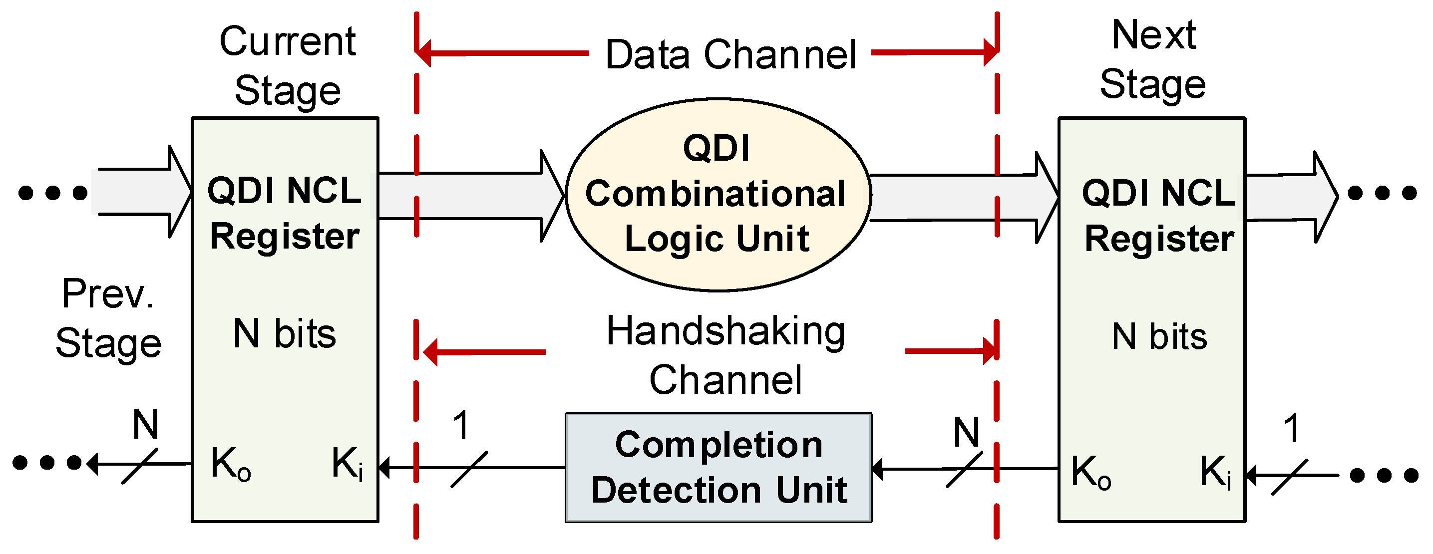
2.1. NCL Framework: An Overview

The NCL framework is depicted in Figure 1, and consists of three primary components: the QDI registration unit, the QDI combinational logic (C/L) unit, and the completion detection unit. In each stage of an NCL pipeline, a C/L unit is placed between two sets of registers along with a completion detection unit. The C/L unit performs the logic function, while the registration and completion units establish the control path for synchronization in the absence of a reference clock signal. NCL employs one-hot encoding for data to eliminate the timing reference. Dual-rail logic is the most common encoding scheme, which, unlike Boolean logic, requires two wires to represent a single bit of information (i.e., logic ‘0’ or ‘1’), simultaneously representing both literals of the variable. A dual-rail variable, X, consists of two wires/rails X0 and X1 that can have one of the three legal values from the set {NULL, DATA0, DATA1}, where X0 (and X1) ϵ {0, 1}. DATA0 (X1 = 0 and X0 = 1) and DATA1 (X1 = 1 and X0 = 0) are the equivalents of Boolean logic ‘0’ and ‘1’, respectively. When both rails are ‘0’, it indicates a NULL state, which serves as a filler state between two distinct data fronts. As per the dual-rail protocol, both rails of a signal cannot be asserted simultaneously, making X0 = X1 = 1 an illegal state. Together, the registers and the completion units maintain a sequence of alternating NULL and DATA to differentiate between two distinct DATA wavefronts at the input and their corresponding DATA wavefronts at the output [16].
NCL circuits are comprised of 27 fundamental threshold gates that constitute the set of all functions consisting of up to four non-inverted variables, where each rail of a multi-rail data signal is considered a separate variable. The gates have state-holding capability, known as hysteresis, which necessitates that all inputs be de-asserted to de-assert an already asserted output. The hysteresis ensures that all current input data wavefronts transition to NULL prior to computing the output associated with the next input data wavefront. The gates are classified into two categories: weighted and unweighted. An unweighted gate is denoted as THmn, where n represents the number of inputs and m represents the threshold value (i.e., minimum number of inputs that must be asserted to assert the gate output), which ranges from 1 to n. A weighted gate is expressed as T H m n W w 1 , w 2 , w r , where w r   ( 1 < w r m ) signifies the weight of the input r [16]. Figure 2a depicts an NCL TH13 gate with three inputs (A, B, and C) and a threshold value of 1, indicating that the output will be asserted when at least one of the inputs is asserted. Therefore, the set function of TH13, FTH13, becomes A + B + C. Figure 2b shows a weighted TH24w22 gate, which has four inputs (A, B, C, and D), with the first two inputs (A and B) having a weight of 2 and the remaining inputs (C and D) each having a weight of 1. To assert the gate output, a minimum threshold of two must be met. Therefore, the set equation of TH24w22, FTH24w22, becomes A + B + CD.
Each one-bit NCL register comprises two TH22 gates and one inverting TH12 gate (TH12n). The TH22 gates allow an input DATA to pass at the output only when the Ki input is rfd (request-for-data, i.e., logic 1) and an input NULL to pass only when the Ki input is rfn (request-for-null, i.e., logic 0). The TH12n gate produces a Ko output, which is rfd if a NULL is latched and rfn when a DATA is latched. Each completion unit consists of a tree of THnn gates that combines all N-bit Ko signals from the subsequent stage registers into a single Ko output, which then serves as the Ki input of the previous stage registers. The gate level structure of NCL registers and completion units can be found in [16].
NCL C/L must be designed to be both input-complete and observable to preserve delay-insensitivity. Input completeness dictates that a C/L unit’s outputs cannot transition from NULL to DATA until all inputs have transitioned from NULL to DATA. Likewise, all outputs of a C/L unit must not transition from DATA to NULL until all inputs have made the transition from DATA to NULL [16]. However, according to Seitz’s ‘weak conditions’ of delay-insensitive signaling [17], in C/L units with multiple outputs, it is permissible for some of the outputs to transition without a complete set of inputs, as long as all outputs do not manage to transition before all inputs arrive. Observability necessitates that each gate transition be observable at the output, which means that each transitioning gate must also transition at least one output [16].

2.2. Error-Resilient QDI Architectures

Resiliency schemes that are widely utilized and appropriate for traditional synchronous designs lack direct applicability to the asynchronous domain due to their unique architecture and demonstration of different responses to soft errors. For example, triple modular redundancy (TMR) [18], a common resiliency approach for clocked designs, requires making three copies of the circuit, where the correct output comes to be determined by a majority voting logic scheme. In QDI circuits, implementing the majority voting technique, synchronizing across three copies of the circuit, and ensuring deadlock-free operation can be challenging [4]. In addition, NCL circuits are inherently area-heavy, and making three copies of the circuit can restrict their application due to a much larger area requirement.
The architecture and delay-insensitive nature of QDI circuits inherently confer a certain level of resilience against soft errors. Monnet et al. studied the effects of timing variations induced by transient faults in QDI circuits [19]. The study concluded that QDI circuits offer a degree of resistance to timing variations, which may arise from alterations in transistor threshold voltages resulting from charge accumulation through particle striking. Furthermore, the dual-rail implementation can aid in easier detection of an SEU. An example of this would be the generation of an invalid DATA value of ‘11’ by a single-rail upset in a DATA variable (10 or 01), which would trigger automatic error detection. Utilizing the advantages of such QDI properties, Kuang et al. [20] proposed an NCL architecture with an integrated soft-error corrector that built upon the concept introduced by Gardiner et al. [21]. In this method, the original NCL architecture is modified by introducing additional logic and registration stages, ensuring correct re-computation of the C/L unit once an error is detected. The method can detect and correct soft errors that result in illegal DATA values during a DATA phase; however, errors that transpire during the NULL phase of operation cannot be corrected by the proposed architecture. Ref. [22] addressed this issue and modified the architecture further to detect and correct errors in NULL phases as well. However, Ref. [23] illustrated that, despite the modifications made to the architecture, it may still fail to ensure complete resilience under certain corner case error scenarios. Moreover, both [20,22] impose a performance penalty in the form of increased latency, as they both necessitate the pipeline to come to a halt until the error effects completely subside.
A duplication-based dual modular redundancy (DMR) approach was proposed in [24] to design resilient NCL circuits. This approach guarantees the pipeline’s full recovery in the event of an SEL/SEU, while preventing the occurrence of incorrect data or circuit deadlock. The approach was modified in [25] to mitigate multi-bit SEUs. Moreover, this approach was further tailored and extended to design SEL/SEU-tolerant QDI SCL circuits as well [26]. A duplication- and double-checking-based approach was successfully implemented to design QDI PCHB and WCHB circuits that are entirely resistant to SEUs [27,28,29]. Furthermore, a duplication-based approach was utilized in [30] to enhance the fault tolerance at the threshold gate level in NCL circuits, operating at subthreshold regime. While duplication-based methods can ensure complete resilience, they all incur substantial area and energy costs as a result of additional control signals and duplication.

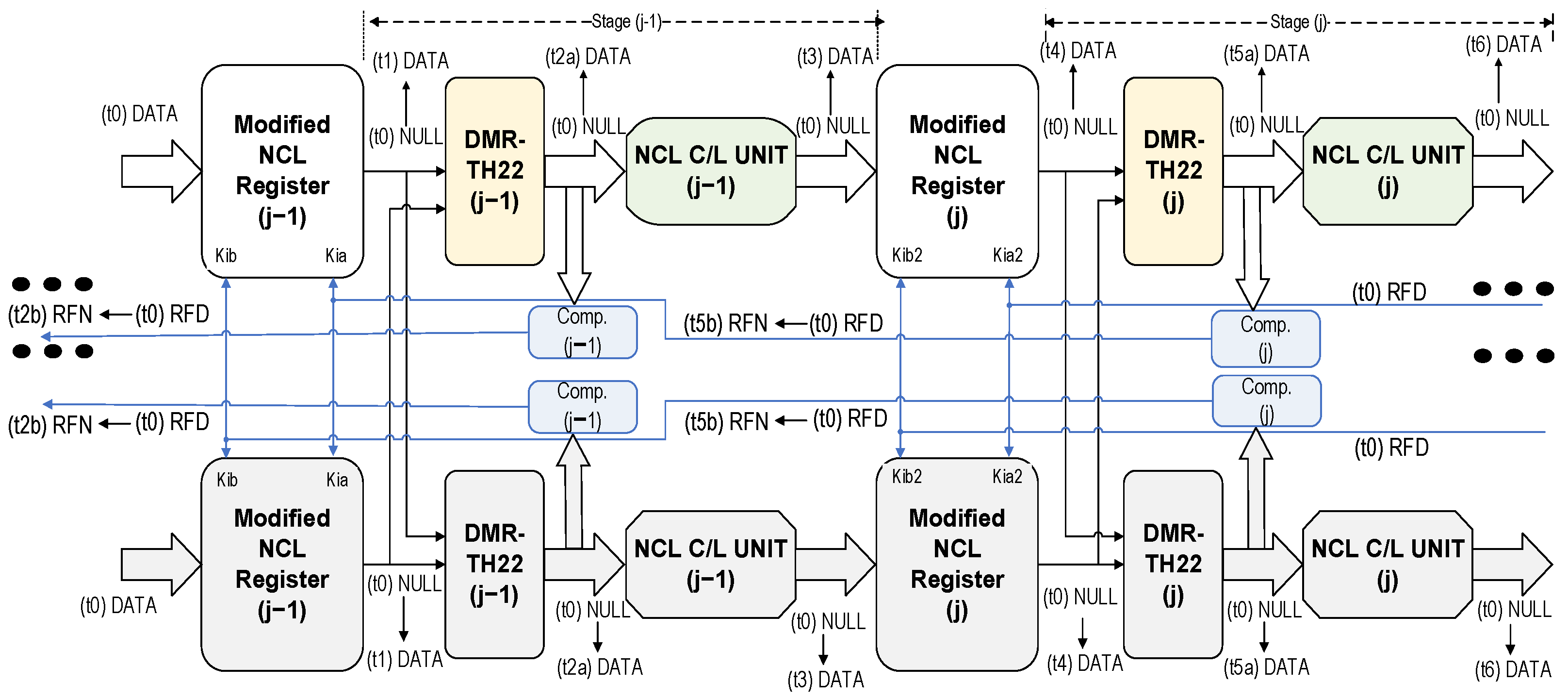
2.3. Dual Modular Redundancy (DMR)-Based NCL (DMR-NCL) Architecture

In DMR-NCL architecture, the original NCL pipeline is doubled, as shown in Figure 3, with the shaded sections depicting the duplicated pipeline. During an SEL/SEU occurrence, the architecture ensures error-free data propagation through the pipeline by performing parallel computations on both the original and duplicate circuits, followed by an output consistency check. Apart from the duplication, the following modifications are incorporated: (i) at the outputs of each registration stage in both copies, an additional stage of TH22 gates is added to prevent the propagation of mismatched data between the two copies. We refer to this stage as DMR-TH22, as depicted in Figure 3; (ii) the conventional register structure is modified and the TH22 gates within each register are substituted by TH33 gates, allowing each register to receive two request (Ki) inputs—one from each copy’s completion output in the succeeding stage to establish the dependency between the two copies of the circuit; and (iii) the registers no longer generate acknowledge outputs (Ko) because the TH12n gates have been removed. These TH12n gates are instead placed in the first level of the completion components. The completion component in each stage receives inputs from the outputs of the DMR-TH22 gates in the same stage and generates an output that is supplied to one of the Ki inputs of the registers in the previous stage in both copies.
The flow of DATA through the various stages of the DMR-NCL pipeline is also illustrated in Figure 3. Assume that, at time t0, new DATA is available at Regj−1 inputs and all other stages are in the NULL state. Since the succeeding stage, stagej, is requesting data (RFD), Regj−1 will latch the DATA in both copies at time t1. At t2a, the matched DATA will be allowed to pass through the DMR-TH22 gates. Both the completion components in stagej−1 detect the DATA at their corresponding DMR-TH22 outputs and evaluate to logic ‘0’, requesting for the next NULL (RFN) (time t2b). At time t3, the C/L units in both copies complete their computation and provide the computed DATA to the next stage, stagej, which is latched by the stagej registers at time t4. The DATA continue to propagate through stagej in the same fashion as stagej−1. When the NULL signal becomes available, the flow of NULL through the various stages of the DMR-NCL pipeline will also adhere to comparable transitions.

3. Proposed Formal Framework for the Verification and Vulnerability Analysis of DMR-NCL Architecture

This section describes the proposed formal verification method developed to verify the correct operation of DMR-NCL circuits synthesized from their synchronous/Boolean counterparts using design automation tools. There are four distinct high-level steps in the verification procedure. In the first step, the synthesized DMR-NCL circuit is subjected to a circuit abstraction procedure, resulting in the conversion of the original DMR-NCL circuit to an equivalent Boolean/synchronous circuit. The converted netlist is then checked against the circuit’s original synchronous/Boolean specification for equivalence in the second step. In the third step, additional invariant checks are conducted to validate the integrity of each dual-rail signal, thereby ensuring the mutual exclusivity property of each dual-rail signal. In the fourth and final step, additional checks are performed to ensure deadlock-free operation of the synthesized DMR-NCL circuits. This section also includes an exhaustive list of all possible synthesis errors, which will be used to demonstrate the effectiveness of the developed tool in detecting these errors post-synthesis, as described in Section 5.

3.1. Comprehensive Set of Possible DMR-NCL Synthesis Faults: A Case Study

Existing design and optimization methodologies for NCL circuits, such as NCL_D [8], NCL_X [9], UNCLE [11], Nowick’s Relaxation [31,32], Enhanced Relaxation [33], Prime Indicants [34], etc., employ commercially available design automation tools for logic synthesis. In many of these techniques, e.g., NCL_D and UNCLE, the synthesis begins with the register transfer level (RTL) description of the circuit’s synchronous/Boolean specification. Initially, the specification becomes converted into a netlist comprising only two-input Boolean functions, which is referred to as a 3NCL netlist. Then, each single-rail signal is transformed into a dual-rail signal, and each gate function is expanded into its dual-rail counterpart, followed by a series of optimization procedures, such as logic minimization, gate mapping, cell merging, etc. The registers and completion components are then added, and handshaking connections are established in accordance with the four-phase handshaking protocol. Identical procedures can be followed to automate the synthesis of DMR-NCL circuits. The goal of our proposed methodology is to verify the correct functionality of the DMR-NCL circuits that are synthesized from their synchronous counterparts. The proposed verification method ensures the functional equivalence between the synchronous specification and the DMR-NCL implementation, while also ensuring that the circuit never deadlocks during operation. Note that the proposed method assumes that the transistor-level implementation of threshold gates as well as the NCL registers are correct, which is consistent with standard gate-level verification practices [35]. Since each gate and register component is small enough, exhaustive simulations, a common technique for verifying circuit primitives, can be used to verify them with relative ease. Moreover, note that the proposed method does not verify the input completeness and observability of the C/L units, as these can be validated separately using existing formal methods, as described in [13,36].
The following Is an exhaustive list of potential errors that may occur during DMR-NCL synthesis.
Error Case 1: Incorrect logic synthesis—as discussed earlier, the synthesis process includes multiple logic optimization and minimization schemes. For instance, a two-input NAND function followed by a two-input NOR function can be merged and substituted by a three-input AND function during optimization (e.g., [ A . B + C ] can be implemented using a three-input AND function with inputs A ,   B ,   a n d   C ). In this scenario, incorrect gate-mapping can lead to the merging function being implemented using a three-input OR function instead, or the C input not being inverted, resulting in improper circuit functionality.
Error Case 2: Incorrect gate connection in the C/L unit—this case corresponds to a scenario in which a gate, gatei, that should be connected to gatej is instead connected to gatek. For example, the output of a TH12 gate with set function, FSET = A + B, should be connected to one of the inputs of TH22 (FSET = AB) in an error-free scenario. However, the TH12 gate output comes to be improperly connected to a TH23w2 gate with a set function, FSET = A + BC, resulting in incorrect logic implementation.
Error Case 3: Swapped rail connection—in dual-rail logic, a signal inversion occurs when the rails of a dual-rail signal are switched. Consider a direct connection between two NCL functions, A and B, where the dual-rail output, F, of function A should be connected to one of the dual-rail inputs, X, of function B. This connection requires F.rail0 and F.rail1 to be directly connected to the corresponding rails, X.rail0 and X.rail1, of function B, respectively. However, an erroneously swapped rail connection would result in F.rail0 and F.rail1 being connected to X.rail1 and X.rail0, respectively. This would result in F’ being connected to X instead of F, leading to a logical error caused by the signal inversion. This is true for a connection between a dual-rail NCL register and NCL function as well.
Error Case 4: Incorrect rail connections—both rails of a dual-rail NCL function input, register input, or primary output should be derived from the same variable; otherwise, illegal dual-rail values may be generated. Assume that X is a dual-rail input of an NCL function, which receives its rail0 and rail1 wires from two different signals, F.rail0 and G.rail1, respectively. This will result in an illegal value for X (i.e., X.rail0 = X.rail1 = 1) if F becomes DATA0 (i.e., F.rail0 = 1 and F.rail1 = 0) and G becomes DATA1 (i.e., G.rail0 = 0 and G.rail1 = 1). Alternately, if F and G become DATA1 and DATA0, respectively, X will remain NULL.
Similarly, both rails of a dual-rail NCL function input, register input, or primary output should not comprise the same rail of a dual-rail signal. Consider that both rails of the X input of an NCL function are connected to the F.rail1 output of another NCL function. This will prevent X from transitioning to DATA when F is DATA0 and evaluate to an illegal data value when F is DATA1. Both types of rail errors can result in improper outputs and deadlock in an NCL circuit.
Error Case 5: Control signals connected to data ports—the acknowledge output, Ko, generated by a completion detection unit may be improperly connected to one or more NCL threshold gates in the C/L and DMR-TH22 network, data input(s) of NCL registers, or data input of another completion unit. This can potentially violate the four-phase handshaking protocol and result in circuit deadlock and/or erroneous output.
Error Case 6: Incorrect gate type in the circuit—since NCL is synthesized from a synchronous/Boolean specification, the synthesized circuit can contain unexpanded single-rail Boolean gates. Lacking hysteresis, Boolean gates can influence the delay insensitivity of an NCL circuit.
Error Case 7: Incorrect DMR-TH22 connections—the purpose of DMR-TH22 gates is to block unmatched DATA between the two copies of the circuit during SEU/SEL. To accomplish this, identical output rails of each register in a stage from both copies must be connected to a single DMR-TH22 gate. Failure to maintain this connection may result in deadlock or incorrect computation. For instance, consider a dual-rail register, Rega, in the original copy of the circuit with output, F. The corresponding shadow (or duplicate) register, Regb, has G as its dual-rail output. In an error-free scenario, there should be two DMR-TH22 gates following the two registers, one in the rail0 network with F.rail0 and G.rail0 as inputs, and the other in the rail1 network with F.rail1 and G.rail1 as inputs. However, suppose a synthesis error occurs in the DMR-TH22 gate in the rail0 network, in which the G.rail1 rail is incorrectly connected instead of the G.rail0 rail. In such a scenario, the registers transitioning from NULL to DATA0 will be unable to update the DMR-TH22 gate in the rail0 network. Therefore, DATA0 will not be permitted to pass, even though both register outputs match. This will eventually result in circuit deadlock.
Error Case 8: Non-TH22 gates at register outputs—TH22 gates behave like two-input C-elements [37], which evaluate to 1 or 0 only when both of their inputs are 1 or 0, respectively. If the two inputs are different, the gate maintains the previous value, i.e., it does not update. Therefore, the C-element-like behavior of DMR-TH22 gates at the register outputs in both copies of the circuit is used to allow only matched DATA/NULL to flow through both pipelines and block unmatched DATA. A non-TH22 gate at register outputs will fail to serve this purpose and may result in deadlock, incorrect outputs, or both.
Error Case 9: Missing signals in the completion unit—as per the DMR-NCL handshaking protocol, every completion unit acknowledges all preceding stage register outputs that took part in calculating the stage’s register inputs. To maintain this, after being filtered by the stage’s DMR-TH22 gates, each rail of the N-bit register outputs must be an input to the stage’s completion unit, and the output of the completion unit must be connected to one of the two Ki inputs of the registers in the previous stage in both copies of the circuit. The absence of one or more of the required signals in the completion unit inputs may result in the premature generation of a NULL/DATA request, which, in certain timing scenarios, can result in circuit deadlock.
Error Case 10: Additional signals in the completion unit—A completion component may incorrectly contain additional signals from the DMR-TH22-filtered register outputs from other stages. This may cause circuit deadlock, especially when the pipeline contains the maximum amount of distinct DATA tokens, but it could also function correctly. Each additional signal would, therefore, require additional inspection. Moreover, any additional input signal to a completion unit that is not generated by a DMR-TH22 gate is invalid.
Error Case 11: Incorrect gates (non TH12n/THnn) in the completion circuitry—the completion component in a DMR-NCL circuit comprises a series of TH12n gates at the first level, followed by a tree of THnn gates, which combines N dual-rail signals into a single Ko output. Any other gate in the completion circuitry is an error, which may cause deadlock in a circuit.
Error Case 12: Incorrect TH12n input(s) in the first level of the completion circuitry—there are N number of TH12n gates in the first level of an N-input completion unit. Each TH12n gate receives both rails of the same dual-rail signal as inputs, which evaluates to ‘0’ when either rail is ‘1’ (i.e., the dual-rail signal is DATA0/DATA1), and to ‘1’ when both rails are ‘0’ (i.e., the dual-rail signal is NULL). Hence, the series of TH12n gates in the first level of each completion unit acts as a NULL/DATA detector for that stage. When a NULL/DATA is detected, the logic ‘1’/‘0’ outputs of all the TH12n gates are combined utilizing a THnn tree structure to generate a one-bit single-rail request-for-DATA (rfd, i.e., Ko = 1)/request-for-NULL (rfn, i.e., Ko = 0) signal. If one or more of the TH12n gates receives incorrect inputs, such as the same rails of a dual-rail signal or rails from two different signals, it will fail to detect the corresponding NULL/DATA signal value. Consequently, even when all inputs are NULL/DATA, the completion unit will not generate the correct request signal, resulting in circuit deadlock.
Error Case 13: External Ki connection error—the external Ki inputs must be connected to the Ki inputs of the registers in the last stage to synchronize all the primary outputs. A missing external Ki connection will cause circuit deadlock under some timing scenarios.
Error Case 14: External Ko connection error—the external Ko outputs synchronize the primary inputs in both copies of the circuit. Therefore, the completion unit in the initial stage in a copy must include the DMR-TH22-filtered output signals of all the initial stage registers that accept primary inputs in that copy. Any missing or incorrectly connected signal in the completion component will cause circuit deadlock.
Error Case 15: Data signals connected to a register’s Ki ports—each register has two Ki input ports. If the register is not in the final stage, it should receive one of the Ki inputs from the output of the succeeding stage’s completion unit in the same copy, while it should receive the other Ki input from the output of the succeeding stage’s completion unit in the other copy. Otherwise, the Ki inputs should be connected to the external Ki signals if the register is in its final stage. Any rail of a data signal cannot be connected to the Ki inputs of a register, as this would result in circuit deadlock.
Error Case 16: Shorted output—an output of any C/L unit and/or DMR-TH22 gate, completion unit, or register unit, cannot have a shorted connection with any other gate outputs, register outputs, completion outputs, primary data inputs, external Ki inputs, or external Ko outputs. This will result in undefined values for the shorted signals.
Error Case 17: Floating input(s) in components—an input signal to a gate in the C/L unit and/or DMR-TH22 gate(s), completion unit, or register unit, must be derived from the output of another component in the design—or from a primary input, if appropriate according to the design rules of the DMR-NCL architecture. Otherwise, the signal will be floating. This may happen during synthesis if, for example, the component driving the signal is removed or the signal is updated in some but not all locations where it is used.
Error Case 18: Illegal interconnection between two copies of the circuit—as per the DMR-NCL architecture, the inputs to a C/L unit, the data inputs to a register, and the inputs to a completion unit in the original copy cannot be derived from any component in the duplicate copy, or vice versa. A violation of this connection protocol can impact the circuit recovery procedure during SEL/SEU, leading to incorrect outputs, and resulting in circuit deadlock.

3.2. Proposed Safety Check

The safety check procedure has two steps. A functional equivalence check is conducted initially to compare the synthesized DMR-NCL circuit with its synchronous specification. In this step, the rail1 network is the primary focus, given that the Boolean outputs of the synchronous specification correspond to the rail1 signals of the DMR-NCL output variables. The rail0 network is validated in the second step. Both the steps are detailed in this section.

3.2.1. Functional Equivalence Check

We have used a two-stage 3 × 3 DMR NCL multiplier, as depicted in Figure 4, as an example circuit to illustrate the safety check procedure. As per the DMR architecture in Figure 3, there are two copies of the multiplier, one original and one duplicate (highlighted in gray), implementing the output function p 5 : 0 = x i 2 : 0 × y i 2 : 0 . Both the original and duplicate circuits are identical and, therefore, the complete structure of the duplicate circuit is not shown in the figure. The inputs, outputs, and intermediate signals of both the actual and duplicate circuits are dual rails. The combinational logic (C/L) unit comprises both input-complete (denoted with a C inside the AND symbol) and input-incomplete (denoted with an I inside the AND symbol) NCL AND functions, NCL Half-Adders (HA), and NCL Full-Adders (FA). The internal structures of the NCL AND, NCL HA, and NCL FA functions can be found in [16]. Each copy of the circuit contains three sets of registers: input registers, output registers, and intermediate registers that are all reset-to-NULL (Reg_NULL). Note that the circuit can be designed with only the I/O registers; however, an intermediate registration stage is added to make the circuit more generic and to better explain each step of the procedure. Following registration, each stage contains a series of DMR-TH22 gates at the same level, each of which receives the same rail of a particular register output from its original and corresponding duplicate copies. Each completion detection unit within a stage accepts the stage’s DMR-TH22 outputs as inputs and generates an acknowledgment output, Ko, which acts as a request signal (Ki) for the previous stage’s registers in both copies of the circuit.
Figure 5a displays the netlist format for the 3 × 3 DMR NCL multiplier, referred to as NCLInitial. This netlist structure is generated from the circuit’s RTL-level description in Verilog HDL. The primary inputs and primary outputs of both the original and duplicate circuits are listed in lines 1 and 2, respectively. rail0 and rail1 of a signal are denoted by the extensions ‘_0’ and ‘_1’, respectively. Lines 3–166 correspond to the NCL C/L threshold gates. For a threshold gate, the first column specifies the gate_type, the second column lists the gate inputs separated by commas, and the final column specifies the gate output. Lines 167–206 correspond to the one-bit dual-rail NCL registers, where the first column indicates the reset_type (i.e., reset-to-NULL, DATA0, or DATA1); the second column denotes the register level (the depth of the path through the registers, excluding the C/L in-between); the third and fourth columns correspond to the rail0 and rail1 data inputs, respectively; and the fifth column corresponds to the Ki inputs in a comma-separated format, followed by the rail0 and rail1 data outputs in the last two columns, respectively. In the 3 × 3 DMR NCL multiplier example, there are three stages of reset-to-NULL registers with levels 1, 2, and 3, starting from the input registers. Note, as the multiplier in the example is a combinational circuit without feedback paths, reset-to-DATA registers are not required as an initial state indicator. Lines 207–212 are the completion units, where Comp_n (or Comp_ns) in the first column denotes a completion component in the circuit’s original (or duplicate) copy, where ‘n’ is a unique identifier, the second column indicates the inputs in a comma-separated format, which comes from the same stage’s DMR-TH22 outputs, and the last column is the output. Note that each completion component comprises a level of inverting TH12 gates (TH12n) followed by THnn NCL gates arranged in a tree structure [24]. When processing the original RTL-level netlist, the proposed tool combines all the completion unit gates into the single completion component module, such as Comp_1 in Figure 5a (line 207), to simplify the verification process.
The NCLInitial netlist is fed as an input to a Python-based automated safety check tool that we have developed. The netlist undergoes a conversion algorithm that converts the NCLInitial netlist into an equivalent Boolean netlist, referred to as NCLBool, as shown in Figure 5b. During the conversion process, the reset-to-NULL registers (Reg_NULL) and completion units (Comp_n) are removed as they exist solely for control and synchronization purposes and do not affect functionality. Note that the connection between registers and completion units will be verified as a part of the liveness and handshaking check, as elaborated on later. Each NCL threshold gate comes to be replaced with its equivalent hysteresis-less Boolean SET function. Each individual rail of a dual-rail signal is regarded as a separate Boolean signal. Each primary dual-rail input signal is substituted with its rail1 signal, as shown in line 1 in NCLBool in Figure 5b, since rail1 represents the equivalent Boolean logic for a dual rail signal. Line 2 lists the set of primary outputs, which consists of both rail0 and rail1 signals. Lines 3–14 of the converted netlist contain a list of inverters that are added to generate signals equivalent to the eliminated rail0 inputs. Lines 15 and onward specify the converted NCL gates, following the same gate format as NCLInitial. Algorithm 1 outlines the proposed netlist conversion algorithm.
Algorithm 1: Procedure to generate an equivalent Boolean circuit from a DMR-NCL circuit
//Input to the procedure: NCLInitial; Output of the procedure NCLBool//
1:     Create list_pIs (rail1.data_inputs(NCLInitial))
2:     Create list_pOs (data_outputs(NCLInitial))
3:     Create NCL_comp (NCLInitial)
4:     for i← to component_count do
5:                  if NCL_comp(i).instance_type == Reg_NULL then
6:                             merge NCL gates separated by NCL_comp(i)
7:                             delete NCL_comp(i)
8:                  end if
9:     end for
10: for i← to component_count do
11:              if NCL_comp(i).instance_type == Comp then
12:                            delete NCL_comp(i)
13:              end if
14: end for
15: for j← to list_pIs do
16:              generate_rail0_signals (list_pIs(j))
17: end for
18: for i← to component_count do
19:              convert_to_Boolean (NCL_comp(i))
20: end for
The converted Boolean netlist is then compared against the corresponding Boolean specification function (FBool_Spec). The converted netlist is first encoded in the Satisfiability Modulo Theory Library (SMT-LIB) language [38,39] using an automated encoding algorithm that we have developed, which is then input to the Z3 SMT solver [40] to check for equivalence between the converted Boolean netlist and the specification. To verify the functionality of any combinational DMR-NCL circuit, we checked the following generic proof obligation.
Proof Obligation 1 (PO1): 
P 1 :   n = 1 q ( i n A 1 , , i n A q ) = ( i n B 1 , , i n B q )
P 2 :   ( g A 1 , , g A k ) = NCL Bool Step   ( i n A 1 , , i n A q )
P 3 :   ( g B 1 , , g B k ) = NCL Bool Step   ( i n B 1 , , i n B q )
P 4 :   n = 1 l   O u t A n R 1 = O u t B n R 1 = F B o o l _ S p e c .
P O 1 :   { P 1 P 2 P 3 P 4 }
* Note that the suffixes A and B are used to differentiate the signals originating from copy A (original) and copy B (duplicate) of the circuit, respectively. □
Proof Obligation 1, PO1, states that in a converted equivalent Boolean DMR-NCL circuit with q original circuit inputs ( i n A 1 , , i n A q ) and q duplicate circuit inputs ( i n B 1 , , i n B q ) , k threshold gates for both the original and duplicate circuits ( g A 1 ,…, g A k ) and ( g B 1 ,…, g B k ), respectively, and l original circuit outputs ( O u t A 1 , , O u t A l ) and l duplicate circuit outputs ( O u t B 1 , , O u t B l ), if the inputs to the both the original copy (A) and duplicate copy (B) of the circuits are the same (P1), then after each step of the circuit’s execution (P2 and P3), the rail1 outputs of both the copies should match the corresponding Boolean specification (P4).
In case of the 3 × 3 DMR-NCL multiplier, the Z3 SMT solver validates the following safety check property: F N C L B o o l ( x i [ 2 : 0 ] _ 1 , x i s [ 2 : 0 ] _ 1 , y i [ 2 : 0 ] _ 1 , y i s [ 2 : 0 ] _ 1 ) = M U L T   x [ 2 : 0 ] ,   y [ 2 : 0 ] , where ( x i 2 _ 1 ,   x i 1 _ 1 , x i 0 _ 1 ) and ( x i s 2 _ 1 ,   x i s 1 _ 1 , x i s 0 _ 1 ) are the x rail1 inputs to the original circuit A and its duplicate copy circuit B, respectively; ( y i 2 _ 1 ,   y i 1 _ 1 , y i 0 _ 1 ) and ( y i s 2 _ 1 ,   y i s 1 _ 1 , y i s 0 _ 1 ) are the y rail1 inputs to the original circuit A and its duplicate copy circuit B, respectively; and M U L T is the 3 × 3 unsigned Boolean multiplication function as the specification. Although we utilize the Z3 SMT solver for equivalence checking, other combinational equivalence checkers could also be used to verify the proposed safety check property. In this phase of verification, only the rail1 outputs are required to be verified, as these correspond to the Boolean specification circuit outputs, whereas the rail0 outputs are verified via the invariant check, as described next.

3.2.2. Invariant Check for Verifying the rail0 Network

The functional equivalence check only utilizes the abstracted netlist, NCLBool, and the rail1 outputs. However, it is necessary to verify the safety of rail0 outputs as well. An additional proof obligation of SMT invariant is required for the original DMR-NCL circuit (NCLInitial) to guarantee the correctness of rail0 outputs. The proposed invariant check property ensures that for every possible state reachable by the original non-converted DMR-NCL circuit (NCLInitial), where all outputs are DATA, the rail0 of each output must be the complement of its corresponding rail1 output, in accordance with the dual-rail protocol.
To generate all possible combinations of valid DATA at the primary outputs of a DMR-NCL circuit, we take the NCLInitial netlist as an input to our tool and then initialize all original and duplicate registers to NULL, all C/L gates to output 0, and all register Ki inputs to rfd (i.e., request for data or logic 1). After this initialization step, the circuit in NCLInitial is stepped with all primary inputs set to DATA. Note that the input to the duplicate pipeline remains identical to that of the original pipeline and the symbolic step encompasses all possible DATA input combinations. As the input DATA flows through all stages of the circuit, it generates all possible combinations of valid DATA at the primary outputs. To ensure that the rail0 outputs correspond to the inverses of the rail1 outputs, the invariant is checked for each primary dual-rail output. The predicates for Proof Obligation 2 (PO2) are shown below for a DMR-NCL circuit with j registers in both the original (A) and duplicate (B) copies, ( R e g A 1 , , R e g A j ;   R e g B 1 , , R e g B j ), k gates in both copies ( g A 1 , ,   g A k ;   g B 1 , ,   g B k ), and l dual-rail outputs in both copies ( O u t A 1 R 0 , R 1 ,…, O u t A l R 0 , R 1   ; O u t B 1 R 0 , R 1 , ,   O u t B l R 0 , R 1 ) , where R0 and R1 are the rail0 and rail1 variables, respectively.
Proof Obligation 2 (PO2): 
P 1 :   n = 1 j ( R e g A n = R e g B n = 2 b 00 )
P 2 :   n = 1 k   [ ( g A n = 0 ) ( g B n = 0 ) ]
P 3 :   n = 1 j   [ ( K i A n = 1 ) ( K i B n = 1 ) ]
P 4 :   n = 1 q [ ( i n A n = 2 b 01 ) ( i n A n = 2 b 10 ) ] ( i n A n = i n B n )
P 5 :   ( g A 1 1 , , g A 1 k ) = NCLStep   ( i n A 1 , , i n A q )
P 6 :   ( g B 1 1 , , g B 1 k ) = NCLStep   ( i n B 1 , , i n B q )
P 7 :   n = 1 l [ ( O u t A 1 n R 0 = ¬   O u t A 1 n R 1 ) ( O u t B 1 n R 0 = ¬   O u t B 1 n R 1 ) ]
P O 2 :   { P 1 P 2 P 3 P 4 P 5 P 6 P 7 }
Predicate P1 requires all dual-rail registers to be reset-to-NULL. P2 and P3 specify that all threshold gates are reset-to-logic-0 and Ki register inputs are initialized to rfd, respectively, indicating all the stages are ready to accept a new DATA wavefront. P4 indicates that the dual-rail primary inputs to both the original and duplicate copies of the circuit are the same DATA. P5 and P6 represent the symbolic step of the circuit (NCLStep), which enables all stages to evaluate, update the threshold gates, and generate a valid output based on the input DATA. Predicate P7 states that the rails of each dual-rail output are complements of each other. Proof Obligation 2 (PO2) ensures that if DATA are allowed to flow from the primary inputs to the primary outputs, then for all possible valid DATA inputs, each output’s rail0, R0, is always the inverse of its respective rail1 output, R1.

3.3. Proposed Liveness Check and Handshaking Connection Verification

Improper connection(s) between threshold gates, registers, and completion components can compromise the liveness of the circuit and cause deadlock. As substantially more signals are required to establish the dependency between the original and duplicate circuits in DMR-NCL, there is a greater probability of erroneous connections between components in DMR-NCL than in conventional NCL circuits. Consider a DMR-NCL circuit with dual copies, A and B, where A and B are the original and duplicate copies, respectively. Each copy comprises #N one-bit registers, #M DMR-TH22 gates that block unmatched DATA between A and B, #G C/L threshold gates, a completion detection unit per stage, #X dual-rail primary data inputs, #Y dual-rail primary data outputs, one external Ki input signal and Ko output signal, and one reset signal. Considering all possibilities, the output of a C/L gatei (non-DMR TH22 gates) in copy A, can have the following interconnection possibilities: it could be connected to (i) input(s) of other gate(s), gatej, in the same stage in copy A, where ij; (ii) input(s) of other gates in the same stage in copy A including gatei (feedback); (iii) input(s) of other gate(s) in a different stage in copy A; (iv) data input(s) of register(s) in the next stage in copy A; (v) data input(s) of register(s) in the same stage in copy A (feedback); (vi) data input(s) of any register in any other different stage(s) in copy A, excluding the same and immediate next stage; (vii) Ki input of any register in copy A; (viii) input(s) of any DMR-TH22 gate(s) in copy A; (ix) input(s) of the completion detection unit in the same stage in copy A; (x) input(s) of completion detection unit(s) in a different stage in copy A; (xi) external reset inputs of either copy; (xii) external Ki inputs of either copy; (xiii) external data inputs of either copy; (xiv) external data output rail(s) of either copy; (xv) external Ko outputs of either copy; (xvi) completion unit output(s) of either copy; (xvii) output(s) of any gate(s) (including DMR-TH22) or register(s) in either copy; and/or (xviii) inputs of any gate (including DMR-TH22), register, or completion component input(s) in copy B. Based on the DMR-NCL architecture, scenarios (i) and (iv) are valid and presumably correct, whereas the remaining 16 scenarios are incorrect. Each DMR-TH22 gate’s output in copy A also has the same 18 possible interconnection scenarios, out of which scenarios (i), (iv), (ix), and (xiv) are the only valid possibilities. Register and completion component outputs have a smaller set of legitimate connection possibilities than C/L and DMR-TH22 gates. Each rail of the dual-rail output of a register in each stage in copy A can only be connected to one DMR-TH22 gate in copy A and one in copy B in the same stage. The output of each completion detection unit in copy A can only be connected to one of the Ki inputs of the preceding stage registers in both copies, i.e., the stagej completion component in copy A must acknowledge the stagej−1 registers in both copies A and B.
As a part of the liveness check, we exhaustively checked all these connections between each component within the circuit to ensure the absence of deadlock. Like the safety and invariant check, the initial DMR-NCL netlist, NCLInitial (as depicted in Figure 5a), is taken as an input for our liveness check procedure. The netlist was then transformed into a graph structure for efficient examination of all connections. Primary inputs and C/L gates have no liveness conditions, as their correctness is verified by the safety check. However, the safety check cannot verify any of the register and completion unit connections as those are eliminated as a part of the circuit abstraction for verifying the functionality. By traversing the graph structure, the tool creates fanout and fan-in lists for all the registers, DMR-TH22 gates, and completion detection units to verify every connection as per the DMR-NCL architecture and handshaking protocol. For instance, for each dual-rail single-bit register, we constructed two fan-in lists, one for the dual-rail DATA input and one for the Ki inputs, and one fan-out list for the dual-rail DATA output. Then, we checked the following conditions: (i) if a register belongs to the original copy (or duplicate copy), its DATA input fan-in list should only contain components from the original copy (or duplicate copy), indicating that the signals are generated by the components in the same copy; (ii) each register’s DATA inputs can originate from the primary inputs (if the register is an input register, belonging to level 1) or else the preceding stage’s C/L gates or DMR-TH22 gates; (iii) the rail0 and rail1 input signals must be associated with the same dual-rail variable; (iv) the Ki inputs of each register should originate from the original and duplicate circuits’ completion component in the succeeding stage or from the original and duplicate circuits’ external Ki inputs (if the register belongs to the final stage); (v) the DATA fan-out list of each dual-rail register should only contain four DMR-TH22 gates in the same stage, comprising original and duplicate DMR-TH22 gates taking the register’s rail1 output as an input as well as the original and duplicate DMR-TH22 gates taking the rail0 output as an input; and (vi) the rail0 and rail1 output signals should belong to the same dual-rail variable. When verifying DMR-TH22 gates based on the components’ fan-in and fan-out lists, we checked the following conditions: (i) both inputs of each DMR-TH22 gate in a given stage should be from the outputs of registers in the same stage; (ii) the inputs should be a pair comprised of one signal coming from a register in the original circuit and the other from its corresponding register in the duplicate copy; if they are not, the gate is flagged as a probable C/L TH22 gate instead of a DMR-TH22 gate, and the register condition (v) described above will fail; and (iii) the output of a DMR-TH22 gate in the original or duplicate copy can be a primary output of the same copy (if the DMR-TH22 gate is in the final stage), a DATA input of a register in the subsequent stage of the same copy, or an input to C/L gates in the same stage of the same copy. For a completion component in each stage, we check the following conditions: (i) the fan-in list must only include DMR-TH22 gates that are in the same stage of the same copy; and (ii) the fan-out list of a completion component in the original/duplicate copy must comprise either a single Ko primary output in the original/duplicate copy if it is a first stage completion component, or the set of all original and duplicate registers in the preceding stage if it belongs to any other stage.

4. Proposed Vulnerability Analysis Framework: SEL/SEU Will Not Cause Incorrect Outputs and/or Deadlock

This section elaborates on our proposed formal framework for analyzing the SEL/SEU vulnerability of the synthesized DMR-NCL circuit, ensuring that the synthesized circuits are capable of entirely recovering from SEL/SEU without causing incorrect outputs and/or deadlock. As per the DMR-NCL protocol, in each copy of the circuit (original or duplicate), the DMR-NCL TH22 gates, C/L unit, and completion detection unit of a given stage and the NCL registers of the subsequent stage are considered as parts of one group that are powered by the same supply. This implies that a DMR-NCL pipeline contains multiple such groups, where each group has its distinct power source. Figure 6 shows one such group within the purple box. When a group encounters a current surge due to SEL, it becomes disconnected from its source to protect the circuitry. Once the power is restored, the gates within the affected group components may output unknown values (logic 1, logic 0, or even a transient voltage between logic 1 and 0), which, if allowed to propagate, can corrupt the subsequent pipeline stages. Our vulnerability analysis ensures that the synthesized DMR-NCL circuit will not cause and allow the propagation of incorrect outputs during an SEL/SEU. For a comprehensive analysis, we evaluate the vulnerability of a DMR-NCL pipeline when it contains the maximum amount of distinct DATA tokens. As per [24], in NCL, the pipeline contains the maximum amount of DATA tokens when two distinct DATA stages are interleaved by only one NULL stage, maintaining an alternating sequence of DATA and NULL wavefronts. Therefore, in the worst-case scenario for a pipeline containing the maximum number of DATA tokens, SEL can affect a specific group under two scenarios: (1) when the affected group registers stored NULL, and the preceding stage latched DATA; and (2) when the affected group registers stored DATA, and the preceding stage latched NULL.
We formally model the recovery procedure of each individual group with separate power source within the DMR-NCL circuit to exhaustively verify that a temporary power outage in one group will not result in incorrect circuit outputs in either of the two scenarios. For that, we have developed an algorithm that parses the original NCLInitial netlist, partitions the circuit, and creates individual submodules for analyzing each of the unique groups. Each submodule contains the following components: the group under test (i.e., DMR-TH22 gates and the subsequent C/L, registration, and completion detection units), the corresponding group components from the duplicate copy, and the DMR-TH22 gates of the succeeding group from both copies. Figure 6 depicts one such submodule, which will be used to formally analyze the SEL recovery procedure of the test group (enclosed in the purple box). Consider scenario 1 from above, in which SEL affects the test group in copy A when Stagej−1 contained DATA and Stagej latched a NULL. The gates within the affected components will be unknown (X) after power restoration. We have formalized a proof obligation, PO3a, which ensures that, under scenario 1, the correct DATA values will be restored by the circuit before passing it on to the succeeding stages. Identical symbolic DATA inputs are supplied to both the original and duplicate copies (predicate P1 of PO3), indicating that the preceding stage registers (not shown in Figure 6) latched DATA prior to SEL occurrence. All the subsequent group’s unaffected DMR-TH22 gates in both copies are initialized to 0, i.e., ( o u t A 1 ,…, o u t A N ) and ( o u t B 1 ,…, o u t B N ) are initialized to NULL, indicating that the succeeding stage latched NULL prior to SEL occurrence (predicate P2), resembling scenario 1. The gates of all the test group components in copy A, i.e., all the C/L unit gates ( g A 1 ,…, g A k ), register gates ( g r e g A 1 ,…, g r e g A p ), and completion detection unit gates ( g c o m p A 1 ,…, g c o m p A r ) are initialized with unknown values using symbolic assignments, resembling the restored phase of the group after a power outage (predicates P3P5). The duplicate group’s register is initialized with the correct NULL value (P6), since the alternate copy will remain intact during SEL. To enable the transmission of DATA to the subsequent stage, the request signals of the affected group’s registers, KiA, and their corresponding duplicate registers, KiB, are made rfd (P7). Note that KiA and KiB are the correct request signals as they are generated by the uncorrupted group in the subsequent stage. Both the original and duplicate circuits are then stepped (P8 and P9), allowing the group components and the succeeding DMR-TH22 gates to update based on the DATA inputs. The registers in the intact copy (copy B) will latch valid DATA (i.e., D1D0 = {10, 01}) based on the C/L unit’s computation, whereas the registers in copy A, presumably affected by SEL, may output corrupted DATA (DATAX, i.e., D1D0 = {1X, X1}), where one of the rails may come to be asserted, while the other rail remains ‘X’. Note that the NCL C/L units are monotonic, i.e., if the inputs to the C/L unit are DATA (DATAX)/NULL, then the outputs will eventually be DATA (DATAX)/NULL. The proof obligation PO3a verifies that the corrupted DATA will eventually be filtered by the succeeding groups’ DMR-TH22 gates, resulting in identical outputs from both partitioned copies in the succeeding stage (P10). This ensures that only the correctly recovered DATA will be transmitted to the subsequent stage even if multiple gates within the test group become corrupted during a SEL occurrence.
Proof Obligation 3 (PO3): 
P 1 :   n = 1 q [ ( i n A n = 2 b 01 ) ( i n A n = 2 b 10 ) ] ( i n A n = i n B n )
P 2 :   n = 1 N ( o u t A n = o u t B n = 2 b 00 )
P 3 :   n = 1 k ( g A n = X )
P 4 :   n = 1 p ( g r e g A n = X )
P 5 :   n = 1 r ( g c o m p A n = X )
P 6 :   n = 1 j ( R e g o u t B n = 2 b 00 )
P 7 :   ( K i A = K i B = 1 )
P 8 :   ( g A 1 1 , , g A 1 k ;   g r e g A 1 1 , , g r e g A 1 p ;   g c o m p A 1 1 , , g c o m p A 1 r ) = NCLStep   ( i n A 1 , , i n A q )
P 9 :   ( g B 1 1 , , g B 1 k ;   g r e g B 1 1 , , g r e g B 1 p ;   g c o m p B 1 1 , , g c o m p B 1 r ) = NCLStep   ( i n B 1 , , i n B q )
P 10 :   n = 1 N [ ( o u t A 1 n = 2 b 01 ) ( o u t A 1 n = 2 b 10 ) ] ( o u t A 1 n = o u t B 1 n )
P 11 : ( K o A 1 = K o B 1 = 0 )
P O 3 a :   P 1 P 2 P 3 P 4 P 5 P 6 P 7 P 8 P 9 P 10
P O 3 b :   P 1 P 2 P 3 P 4 P 5 P 6 P 7 P 8 P 9 P 11
To prove that SEL will not cause deadlock in a DMR-NCL circuit, we need to ensure that the four-phased NCL handshaking protocol will always be preserved. The NCL handshaking protocol dictates that, in an NCL pipeline, a register should permit a new DATA/NULL wavefront to pass only after the previous NULL/DATA wavefront has been acknowledged by the succeeding stage. In other words, the succeeding stage’s completion detection unit should request-for-DATA/request-for-NULL (i.e., output rfd/rfn) only after detecting the complete NULL/DATA at the stage, which allows the previous stage registers to pass the new DATA/NULL wavefront. Unlike NCL registers, DMR-NCL registers receive two Ki inputs, one from each of the original and duplicate copies’ completion detection units in the subsequent stage, and both the Ki signals need to be rfn/rfd for the register to allow NULL/DATA to pass through. This guarantees that a corrupted completion detection unit, such as the Comp1 unit in Figure 6, cannot alone cause a register in the previous stage to pass NULL/DATA by prematurely requesting for NULL/DATA if the other copy, Comp1s, is intact (i.e., not corrupted). As they belong to separate groups, it is highly improbable that both completion detection units in a stage will be compromised at the same time during a SEL. This does not require a separate verification procedure because we assume that the gate-level structure of registers is correct based on component-level testing. Additionally, the liveness check verifies that the registers are receiving the correct Ki inputs, as described in Section 3.1. Hence, it is safe to assume that a register will not allow NULL/DATA to pass if its Ki request signals do not match. However, there is a corner case. Consider the submodule circuit in Figure 6 under scenario 1, where the SEL-affected completion component, Comp1, incorrectly outputs an rfd after power restoration when the corresponding duplicate copy, Comp1s, outputs the correct rfn. In such a scenario, the pipeline will halt and fail to advance if the corrupted completion detection output is not rectified. PO3b checks that, under scenario 1, the SEL-affected completion component will eventually output the correct request signal (rfn in this case; P11) after recomputing, once the DATA flows through the group following power restoration, allowing the circuit to make forward progression.
Similar to PO3, PO4 verifies that a SEL-affected group will not result in incorrect outputs and/or a deadlock when the affected group register stored DATA and the previous stage latched NULL before becoming disconnected from the source (scenario 2). Note that the proof obligations PO3 and PO4, which prove that SEL will not result in inaccurate outputs and/or deadlock in either of the two potential scenarios, also cover SEU occurrences, as SEU only assumes the corruption of a single gate, whereas SEL assumes the corruption of multiple gates within a group.
Proof Obligation 4 (PO4): 
P 1 :   n = 1 q ( i n A n = i n B n = 2 b 00 )
P 2 :   n = 1 j [ ( R e g o u t B n = 2 b 01 ) ( R e g o u t B n = 2 b 10 ) ]
P 3 :   n = 1 N ( o u t A n = o u t B n = R e g o u t B n )
P 4 :   n = 1 k ( g A n = X )
P 5 :   n = 1 p ( g r e g A n = X )
P 6 :   n = 1 r ( g c o m p A n = X )
P 7 :   ( K i A = K i B = 0 )
P 8 :   ( g A 1 1 , , g A 1 k ;   g r e g A 1 1 , , g r e g A 1 p ;   g c o m p A 1 1 , , g c o m p A 1 r ) = NCLStep   ( i n A 1 , , i n A q )
P 9 :   ( g B 1 1 , , g B 1 k ;   g r e g B 1 1 , , g r e g B 1 p ;   g c o m p B 1 1 , , g c o m p B 1 r ) = NCLStep   ( i n B 1 , , i n B q )
P 10 :   n = 1 N [ ( o u t A 1 n = o u t B 1 n = 2 b 00 ) ]
P 11 :   ( K o A 1 = K o B 1 = 1 )
P O 4 a :   P 1 P 2 P 3 P 4 P 5 P 6 P 7 P 8 P 9 P 10
P O 4 b :   P 1 P 2 P 3 P 4 P 5 P 6 P 7 P 8 P 9 P 11

5. Results and Discussions

5.1. Verification Results

As shown in Table 1, the proposed methodology has been demonstrated on multiple unsigned DMR-NCL multipliers of varying widths, extending from 3 b i t × 3 b i t to 10 b i t × 10 b i t multipliers. Since multiplier complexity in terms of number of gates and gate levels grows exponentially with bit size, multipliers are excellent benchmarks for demonstrating the scalability of the verification process. For each circuit, the Z3 runtime for the safety and invariant check and the tool’s runtime for the additional tests performed to ensure the liveness and handshaking check are reported in Table 1. Note that the netlist conversion time and the time required to traverse the graph structure to construct the components’ fan-in and fan-out lists have not been reported because they are negligible as compared to the Z3 runtime. All the bugs were injected into the largest DMR-NCL test circuit, i.e., the 10 b i t × 10 b i t multiplier. B n 10   M u l t circuits correspond to buggy circuits, where ‘n’ corresponds to one of the 18 error case scenarios, as illustrated in Section 3.1. For instance, B 3 10   M u l t corresponds to a bug that results in swapped rail connection during synthesis (error-case 3). In the case of buggy circuits, the (B) next to the runtime indicates whether the bug was discovered during the safety check, invariant check, and/or liveness and handshaking connection check steps of the verification procedure. The verification was carried out on a computer with an Intel Core i7-8550U CPU, 12 GB of RAM, and an operating frequency of 1.80 GHz. Note that the proposed verification methodology does not require the incorporation of additional circuitry to the circuit under verification. The proposed formal framework can be integrated with existing NCL synthesis tools or can be used by itself as a standalone verification tool. In addition, it can be customized for the verification of other redundancy-based QDI paradigms, such as duplication-based resilient PCHB and SCL circuits.

5.2. Detection of All Possible Synthesis Faults

Section 3.1 enumerates 18 different types of errors that can happen during the automated synthesis of DMR-NCL circuits. In this section, we demonstrate how the proposed verification scheme detects all these synthesis faults. Error Cases 1–4 correspond to datapath faults generated by incorrect logic implementations, swapped rails, and/or rail duplication, which are detected during the safety check (i.e., during the functional equivalence check and/or invariant check). Error Cases 5 and 6 are detected during the netlist processing stages, i.e., during the NCLInitial-to-NCLBool-to-SMT language conversion procedure. Liveness and additional checks also detect Error Case 5 as well. Error Cases 7–8, and 16–18 can affect the functionality and/or violate the DMR-NCL protocol, which are detected by both the safety and liveness checks. Error Cases 9–10 and 13–15 are the errors in the handshaking network, which are detected by the liveness and additional checks only. Error Cases 11 and 12 correspond to faults within the internal gate-level circuitry of the completion units, which are detected during the RTL-level netlist processing to generate the NCLInitial format for our tool. During that process, the algorithm combines all the completion unit gates into a single completion component (as shown in Figure 5a). When processing the original DMR-NCL netlist to obtain the abstracted completion component, we ensure that all data inputs to a completion unit go to TH12n gates, and their outputs form a tree of NCL THnn gates to produce a single-bit Ko output. Any discrepancy in the completion unit’s circuitry is reported during this processing stage.
Note that depending on the point of occurrence, certain faults may be detected during the safety check, the liveness and handshaking checks, or both. For instance, both B18(i) and B18(ii) correspond to error case 18: Illegal interconnection between two copies of the circuit. B18(i) is an injected bug that occurs when one of the datapath signals from copy A becomes incorrectly connected to a gate that is in the datapath of the other copy, copy B. On the other hand, B18(ii) represents an injected bug in the control path, where one of the acknowledgment signals from copy A incorrectly replaces a copy B acknowledgment signal in the fan-in of copy B register. While B18(ii) is detected only by the liveness and additional checks, B18(i) is detected by both checks.

5.3. Vulnerability Analysis Results

The vulnerability analysis result is shown in Table 2, based on the Proof Obligation 3 and Proof Obligation 4. The proof obligations were modeled in Satisfiability Modulo Theorem (SMT) language and were tested using the Z3 SMT solver. The vulnerability analysis was carried out on a computer with the same specifications noted above. For each circuit, the Z3 runtime for the vulnerability check is listed in Table 2.

6. Conclusions

The QDI asynchronous design paradigm has emerged as a promising alternative to conventional clock-based digital designs due to its inherent advantages, which include ultra-low power performance, less noise, reduced EMI, and the ability to withstand PVT variations. In addition, the unique architecture provides a certain level of resistance to transient or soft errors that are primarily induced by radiation, but is not completely resilient. Several techniques exist for detecting and mitigating soft errors in QDI circuits, with redundancy-based schemes proving to be the most effective in ensuring complete resilience across all main QDI implementation paradigms, including NCL, PCHB/WCHB, and SCL. This research focuses on one such redundancy-based QDI NCL resiliency scheme known as the dual modular redundancy-based NCL (DMR-NCL) architecture.
Herein, this paper proposes the first ever verification method for formally modeling and validating the correctness of combinational DMR-NCL circuits synthesized from their synchronous counterparts. The methodology can validate both the functional correctness and deadlock-free operation of a circuit. In addition, an exhaustive list of all potential faults that may occur during DMR-NCL synthesis has been presented, and it has been shown that the proposed method can detect each of them. Multiple DMR-NCL combinational benchmark circuits of variable size and complexity were utilized to demonstrate the efficacy of the proposed method. Our approach is fast, scalable, and directly applicable to verify any combinational DMR-NCL circuit synthesized and/or optimized using existing schemes. Note that additional checks would be necessary to assure the input completeness and observability of the synthesized NCL circuits, which already exist in the literature [13,36] and are therefore not discussed in this paper. A formal framework to ensure the capability of synthesized DMR-NCL circuits to correctly recover from SEL/SEU without causing incorrect outputs and/or deadlock has also been presented and demonstrated using the same set of benchmark circuits. Future work will involve extending the proposed approach to verify sequential DMR-NCL circuits and customizing the approach to verify similar redundancy-based QDI SCL and PCHB circuits.

Author Contributions

Conceptualization, D.M. and A.A.S.; methodology, D.M. and A.A.S.; software development, A.C.B.; validation, D.M. and A.A.S.; formal analysis, D.M., A.A.S. and M.D.; investigation, D.M. and M.D.; resources, D.M., A.A.S. and M.D.; writing—original draft preparation, D.M.; writing—review and editing M.D., A.C.B. and A.A.S.; supervision, A.A.S.; project administration, A.A.S.; funding acquisition, A.A.S. All authors have read and agreed to the published version of the manuscript.

Funding

This research was funded by the Woodrow W. Everett, Jr. SCEEE Development Fund in cooperation with the Southeastern Association of Electrical Engineering Heads under Grant No. SCEEE-21-04 and by the National Science Foundation (NSF) under Grant No. CCF-2153373.

Data Availability Statement

The original contributions presented in the study are included in the article, further inquiries can be directed to the corresponding author.

Conflicts of Interest

The authors declare no conflicts of interest.

References

  1. Di, J.; Smith, S.C. (Eds.) Asynchronous Circuit Applications; IET: Stevenage, UK, December 2019; Available online: https://digital-library.theiet.org/content/books/cs/pbcs061e (accessed on 1 November 2023).
  2. Dodd, P.E.; Massengill, L.W. Basic mechanisms and modeling of single-event upset in digital microelectronics. IEEE Trans. Nucl. Sci. 2003, 50, 583–602. [Google Scholar] [CrossRef]
  3. Shoga, M.; Binder, D. Theory of single event latchup in complementary metal oxide semiconductor circuits. IEEE Trans. Nucl. Sci. 1986, NS-33, 1714–1717. [Google Scholar] [CrossRef]
  4. Sakib, A.A. Soft error tolerant quasi-delay insensitive asynchronous circuits: Advancements and challenges. In Proceedings of the 34th SBC/SBMicro/IEEE/ACM Symposium on Integrated Circuits and Systems Design (SBCCI), Campinas, Brazil, 23–27 August 2021; pp. 1–6. [Google Scholar] [CrossRef]
  5. Fant, K.M.; Brandt, S.A. Null convention logic: A complete and consistent logic for asynchronous digital circuit synthesis. In Proceedings of the International Conference on Application Specific Systems, Architectures and Processors: ASAP’96, Chicago, IL, USA, 19–21 August 1996; pp. 261–273. [Google Scholar]
  6. Martin, A.J.; Nystrom, M. Asynchronous Techniques for System-on-Chip Design. Proc. IEEE 2006, 94, 1089–1120. [Google Scholar] [CrossRef]
  7. Zhou, L.; Parameswaran, R.; Parsan, F.; Smith, S.; Di, J. Multi-Threshold NULL Convention Logic (MTNCL): An Ultra-Low Power Asynchronous Circuit Design Methodology. J. Low Power Electron. Appl. 2015, 5, 81–100. [Google Scholar] [CrossRef]
  8. Ligthart, M.; Fant, K.; Smith, R.; Taubin, A.; Kondratyev, A. Asynchronous design using commercial HDL synthesis tools. In Proceedings of the Sixth International Symposium on Advanced Research in Asynchronous Circuits and System, Eilat, Israel, 2–6 April 2000; pp. 114–125. [Google Scholar] [CrossRef]
  9. Kondratyev, A.; Lwin, K. Design of asynchronous circuits using synchronous CAD tools. IEEE Des. Test Comput. 2002, 19, 107–117. [Google Scholar] [CrossRef]
  10. Zhou, Y.; Sokolov, D.; Yakovlev, A. Cost-aware synthesis of asynchronous circuits based on partial acknowledgement. In Proceedings of the IEEE/ACM International Conference on Computer Aided Design, San Jose, CA, USA, 5–9 November 2006; pp. 158–163. [Google Scholar]
  11. Reese, R.B.; Smith, S.C.; Thornton, M.A. Uncle—An RTL approach to asynchronous design. In Proceedings of the IEEE 18th International Symposium on Asynchronous Circuits and Systems, Kgs, Lyngby, Denmark, 7–9 May 2012; pp. 65–72. [Google Scholar] [CrossRef]
  12. Khodosevych, D.; Sakib, A.A. Evolution of NULL convention logic based asynchronous paradigm: An overview and outlook. IEEE Access 2022, 10, 78650–78666. [Google Scholar] [CrossRef]
  13. Sakib, A.A.; Le, S.; Smith, S.C.; Srinivasan, S.K. Formal verification of NCL circuits. In Asynchronous Circuit Applications; IET: Stevenage, UK, 2018; pp. 309–338. Available online: https://digital-library.theiet.org/content/books/10.1049/pbcs061e_ch15 (accessed on 1 November 2023).
  14. Wijayasekara, V.; Srinivasan, S.K.; Smith, S.C. Equivalence verification for NULL convention logic (NCL) circuits. In Proceedings of the 32nd IEEE International Conference on Computer Design (ICCD), Seoul, Republic of Korea, 19–22 October 2014; pp. 195–201. [Google Scholar]
  15. Wijayasekara, V.M.; Rollie, A.T.; Hodges, R.G.; Srinivasan, S.K.; Smith, S.C. Abstraction techniques to improve scalability of equivalence verification for NCL circuits. Electron. Lett. 2016, 52, 1594–1596. [Google Scholar] [CrossRef]
  16. Smith, S.C.; Di, J. Designing Asynchronous Circuits Using NULL Convention Logic (NCL); Morgan & Claypool: San Rafael, CA, USA, 2009. [Google Scholar]
  17. Seitz, C.L. System Timing. In Introduction to VLSI Systems; Addison-Wesley: Reading, MA, USA, 1980; pp. 218–262. [Google Scholar]
  18. Lyons, R.E.; Vanderkulk, W. The use of triple-modular redundancy to improve computer reliability. IBM J. Res. Dev. 1962, 6, 200–209. [Google Scholar] [CrossRef]
  19. Monnet, Y.; Renaudin, M.; Leveugle, R. Asynchronous circuits sensitivity to fault injection. In Proceedings of the 10th IEEE International Online Testing Symposium, Funchal, Portugal, 14 July 2004; pp. 121–126. [Google Scholar]
  20. Kuang, W.; Zhao, P.; Yuan, J.S.; DeMara, R.F. Design of asynchronous circuits for high soft error tolerance in deep submicrometer CMOS circuits. IEEE Trans. Very Large-Scale Integr. (VLSI) Syst. 2010, 18, 410–422. [Google Scholar] [CrossRef]
  21. Gardiner, K.T.; Yakovlev, A.; Bystrov, A. A C-element latch scheme with increased transient fault tolerance for asynchronous circuits. In Proceedings of the 13th IEEE International On-Line Testing Symposium (IOLTS 2007), Heraklion, Greece, 8–11 July 2007; pp. 223–230. [Google Scholar] [CrossRef]
  22. Lodhi, F.K.; Hasan, O.; Hasan, S.R.; Awwad, F. Modified null convention logic pipeline to detect soft errors in both null and data phases. In Proceedings of the IEEE 55th International Midwest Symposium on Circuits and Systems (MWSCAS), Boise, ID, USA, 5–8 August 2012; pp. 402–405. [Google Scholar] [CrossRef]
  23. Lodhi, F.K.; Hasan, S.R.; Hasan, O.; Awwad, F. Analyzing vulnerability of asynchronous pipeline to soft errors: Leveraging formal verification. J. Electron. Test. 2016, 32, 569–586. [Google Scholar] [CrossRef]
  24. Zhou, L.; Smith, S.; Di, J. Radiation Hardened NULL Convention Logic Asynchronous Circuit Design. J. Low Power Electron. Appl. 2015, 5, 216–233. [Google Scholar] [CrossRef]
  25. Brady, J.D. Radiation-Hardened Delay-Insensitive Asynchronous Circuits for Multi-Bit SEU Mitigation and Data Retaining SEL Protection; University of Arkansas: Fayetteville, AR, USA, 2014. [Google Scholar]
  26. Datta, M.; Bodoh, A.; Sakib, A.A. Error Resilient Sleep Convention Logic Asynchronous Circuit Design. In Proceedings of the 2023 21st IEEE Interregional NEWCAS Conference (NEWCAS), Edinburgh, UK, 26–28 June 2023; pp. 1–5. [Google Scholar] [CrossRef]
  27. Jang, W.; Martin, A.J. A soft-error-tolerant asynchronous microcontroller. In 13th NASA Symposium on VLSI Design; Citeseer: University Park, PA, USA, 2007. [Google Scholar]
  28. Jang, W.; Martin, A.J. SEU-tolerant QDI circuits [quasi delay-insensitive asynchronous circuits]. In Proceedings of the 11th IEEE International Symposium on Asynchronous Circuits and Systems, New York, NY, USA, 14–16 March 2005; pp. 156–165. [Google Scholar] [CrossRef]
  29. Jang, W.; Martin, A.J. Soft-Error Tolerant Asynchronous FPGA. In Proceedings of the Dependable System and Network 2005, Rio de Janeiro, Brazil, 22–25 June 2005. [Google Scholar]
  30. Santos, I. Asynchronous Logic Design with Increased Fault Tolerance and Optimized for Subthreshold Operation; The University of Texas at El Paso: El Paso, TX, USA, 2013. [Google Scholar]
  31. Jeong, C.; Nowick, S.M. Optimization of robust asynchronous circuits by local input completeness relaxation. In Proceedings of the Asia South Pacific Design Automation Conference, Yokohama, Japan, 23–26 January 2007; pp. 622–627. [Google Scholar]
  32. Jeong, C.; Nowick, S.M. Block-level relaxation for timing-robust asynchronous circuits based on eager evaluation. In Proceedings of the 14th IEEE International Symposium on Asynchronous Circuits and Systems, Newcastle Upon Tyne, UK, 7–10 April 2008; pp. 95–104. [Google Scholar] [CrossRef]
  33. Khodosevych, D.; Bodoh, A.C.; Sakib, A.A.; Smith, S.C. Combining relaxation with NCL_X for enhanced optimization of asynchronous NULL convention logic circuits. IEEE Access 2023, 11, 104688–104699. [Google Scholar] [CrossRef]
  34. Toms, W.B.; Edwards, D.A. A complete synthesis method for block level relaxation in self-timed datapaths. In Proceedings of the 2010 10th International Conference on Application of Concurrency to System Design, Braga, Portugal, 21–25 June 2010; pp. 24–34. [Google Scholar] [CrossRef]
  35. Sakib, A.A.; Smith, S.C.; Srinivasan, S.K. Formal modeling and verification of PCHB asynchronous circuits. IEEE Trans. Very Large-Scale Integr. (VLSI) Syst. 2019, 27, 2911–2924. [Google Scholar] [CrossRef]
  36. Le, S.; Srinivasan, S.K.; Smith, S.C. Automated verification of input completeness for NCL circuits. Electron. Lett. 2018, 54, 1158–1160. [Google Scholar] [CrossRef]
  37. Muller, D.E. Asynchronous logics and application to information processing. In Switching Theory in Space Technology; Stanford University Press: Redwood City, CA, USA, 1963; pp. 289–297. [Google Scholar]
  38. Monniaux, D. A Survey of Satisfiability Modulo Theory. Available online: https://hal.archives-ouvertes.fr/hal-01332051/document (accessed on 10 September 2023).
  39. Barrett, C.; Fontaine, P.; Tinelli, C. The SMT-LIB Standard: Version 2.6. Tech. Rep.; Department of Computer Science, The University of Iowa: Iowa City, IA, USA, 2017; Available online: www.SMT-LIB.org (accessed on 10 September 2023).
  40. de Moura, L.; Bjørner, N. Z3: An efficient SMT solver. In Tools and Algorithms for the Construction and Analysis of Systems (Lecture Notes in Computer Science); Ramakrishnan, C.R., Rehof, J., Eds.; Springer: Berlin/Heidelberg, Germany, 2008; pp. 337–340. [Google Scholar]
Figure 1. NCL framework.
Jlpea 14 00005 g001
Figure 2. (a) TH13 gate, and (b) TH24w22 gate.
Jlpea 14 00005 g002
Figure 3. DMR-NCL architecture with an illustration of data flow.
Jlpea 14 00005 g003
Figure 4. Unsigned two-stage 3 × 3 DMR-NCL multiplier.
Jlpea 14 00005 g004
Figure 5. (a) Initial 3 × 3 multiplier DMR-NCL netlist, and (b) converted Boolean equivalent netlist.
Jlpea 14 00005 g005aJlpea 14 00005 g005b
Figure 6. Extracted submodule to test the group components enclosed within the purple box.
Jlpea 14 00005 g006
Table 1. Verification time for various combinational DMR-NCL multiplier circuits.
CircuitsVerification Time of Different ProceduresTotal Verification
Safety Check (s)Liveness and Additional Checks (s)Time
(s)
Test Circuits without Bugs
3 × 3 Mult0.060.01550.0755
4 × 4 Mult0.440.01570.4557
6 × 6 Mult1.030.01581.0458
8 × 8 Mult14.480.015914.4959
9 × 9 Mult128.060.0312128.0912
10 × 10 Mult1187.590.03361187.6236
Test Circuits with Injected Bugs
B1 − 10 Mult296.65 (B)0.0336296.774
B2 − 10 Mult1.19 (B)0.03361.224
B3 − 10 Mult296.88 (B)0.0336296.914
B4 − 10 Mult1.48 (B)0.03361.514
B5 − 10 MultIs detected during Netlist Processing0.1220 (B)---
B6 − 10 MultIs Detected during Netlist Processing
B7 − 10 Mult1.55 (B)0.0312 (B)1.581
B8 − 10 Mult1.61 (B)0.029 (B)1.639
B9 − 10 Mult1187.590.03 (B)1187.620
B10 − 10 Mult1187.590.0279 (B)1187.618
B11 − 10 MultIs Detected during Netlist Processing
B12 − 10 MultIs Detected during Netlist Processing
B13 − 10 Mult1187.590.0359 (B)1187.626
B14 − 10 Mult1187.590.031 (B)1187.621
B15 − 10 Mult1187.590.0331 (B)1187.623
B16 − 10 Mult1.35 (B)0.026 (B)1.376
B18(i) − 10 Mult2.39 (B)0.034 (B)2.424
B18(ii) − 10 Mult1187.590.0342 (B)1187.624
Table 2. Vulnerability analysis run-time for various combinational DMR-NCL multiplier circuits.
CircuitsVulnerability Analysis (s)
3 × 3 Mult0.04
4 × 4 Mult0.12
6 × 6 Mult1.11
8 × 8 Mult13.54
9 × 9 Mult85.52
10 × 10 Mult257.41
Disclaimer/Publisher’s Note: The statements, opinions and data contained in all publications are solely those of the individual author(s) and contributor(s) and not of MDPI and/or the editor(s). MDPI and/or the editor(s) disclaim responsibility for any injury to people or property resulting from any ideas, methods, instructions or products referred to in the content.

