2. Processor Micro-Architecture
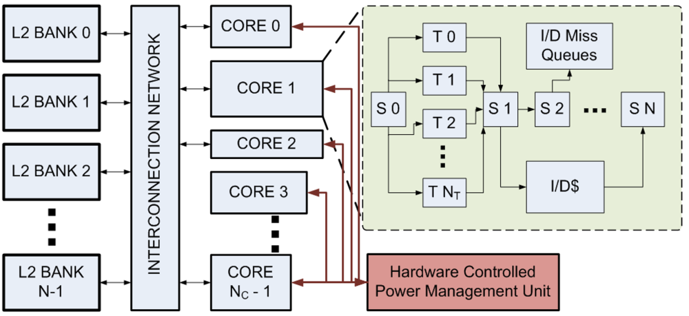
The processor model used in CASPER is shown in
Figure 1. Each core is organized as single-issue in-order with fine-grained multi-threading (FGMT) [
7]. In-order FGMT cores utilize a single-issue six stage pipeline [
8] shared between the hardware threads, enabling designers to achieve: (i) high throughput per-core by
latency hiding; and (ii) minimize the power dissipation of a core by avoiding complex micro-architectural structures such as instruction issue queues, re-order buffers and history-based branch predictors typically used in superscalar and out-of-order micro-architectures. The six stage RISC pipeline is an alteration of the basic simplest five-stage in-order instruction pipeline Fetch, Decode, Execute, Memory and WriteBack. The sixth stage is a single-cycle thread switch scheduling stage which follows a round robin algorithm and selects an instruction from a hardware thread in ready state to issue to the decode stage.
Figure 1.
The shared memory processor model simulated in CASPER. NC heterogeneous cores are connected to NB banks of shared secondary cache via a crossbar interconnection network. Each core consists of S0 to SN are the pipeline stages, T0 to TNT hardware threads, L1 I/D cache and I/D miss queues.
Figure 1.
The shared memory processor model simulated in CASPER. NC heterogeneous cores are connected to NB banks of shared secondary cache via a crossbar interconnection network. Each core consists of S0 to SN are the pipeline stages, T0 to TNT hardware threads, L1 I/D cache and I/D miss queues.
Each core contains
NT number of hardware threads.
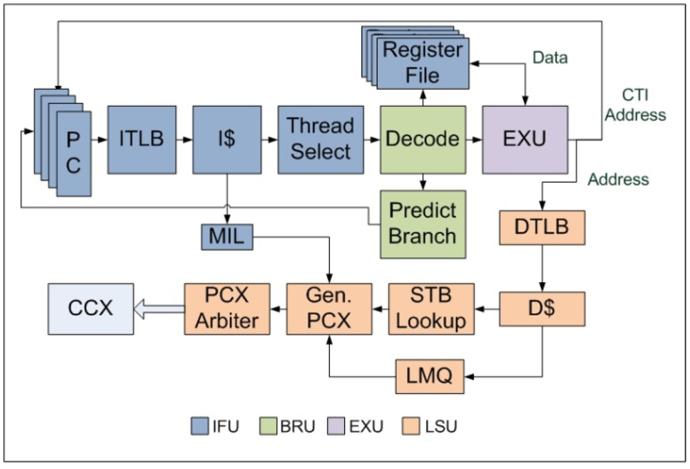
NT is parameterized in CASPER and can be different from one core to another. The 64-bit pipeline in each core is divided into 6 stages—Instruction-Fetch (F-stage), Thread-Schedule (S-stage), Branch-and-Decode (D-stage), Execution (E-stage), Memory-Access (M-stage) and Write-back (W-stage) as shown in
Figure 2.
The F-stage implemented inside Instruction Fetch Unit (IFU) includes the instruction address translation buffer (I-TLB), instruction cache (I$), missed instruction list (MIL) and the integer register file (IRF). MIL is used to serialize I$ misses and send these type of packets from the core to the L2 cache. A similar structure called the Instruction Fetch Queue (IFQ) manages returning I$ miss packets. The size of MIL and IFQ are parameterized in CASPER and is same for all the threads. IRF contains 160 total registers used to support the entire SPARCV9 instruction set. Each hardware thread privately owns IRF, MIL and IFQ whereas I-TLB and I$ are shared. The S-stage which is also part of IFU contains the thread scheduler and thread finite state machine.
Figure 2.
Block diagram of the stages of an in-order FGMT pipeline.
Figure 2.
Block diagram of the stages of an in-order FGMT pipeline.
The D-stage includes a full SPARCV9 instruction set decoder as described in [
19]. Execution Unit (EXU) contains a standard RISC 64-bit ALU, an integer multiplier and divider. EXU constitute the E-stage of our pipeline. Load Store Unit (LSU) is the top level module which includes the micro-architectural components of the M-stage and W-stage. It includes the data TLB (D-TLB), data cache (D$), address space identifier queue (ASIQ), load miss queue (LMQ) and store buffer (SB). LMQ maintains D$ misses. SB is used to serialize the store instructions following the
total store order (TSO) model. Stores are
write through. Both LMQ and SB are separately maintained for each hardware thread while the D-TLB and D$ are shared. Special registers in SPARCV9 are accessed via the ASI queue and ASI operations are categorized as long latency operations as these instructions are asynchronous to the pipeline operation [
19]. Loads and stores are resolved in the L2cache and the returning packets are serialized and executed in the data fetch queue (DFQ) also a part of LSU. The Trap logic Unit (TLU) of SPARCV9 architecture used in CASPER is structurally similar to that of UltraSPARC T1 [
20].
In addition to hardware multi-threading,
clock-gating [
21] in the pipeline stages enables us to minimize power dissipation by canceling the dynamic power in the idle stages compared to active blocks which consumes both dynamic and leakage power. Long latency operations in a hardware thread are typically
blocking in nature. In CASPER, the long latency operations such as load misses and stores are
non-blocking. We call this feature
hardware scouting. This feature optimally utilizes the deeper load miss queues compared to other architectures such as UltraSPARC T1 [
22,
23] where the load miss queue contains only one entry. In average, this enhances the performance of a single thread by 2–5%. The complete set of tunable core-level micro-architectural parameters is shown in
Table 1.
Table 1.
Range and description of the core-level micro-architectural parameters.
Table 1.
Range and description of the core-level micro-architectural parameters.
| Name | Range | Increment | Description |
|---|
| 1. NT | 1 to 16 | Power of 2 | Threads per core |
| 2. MIL Size Per Thread | 1 to 32 | Power of 2 | Used to enqueue the I$ misses |
| 3. IFQ Size Per Thread | 1 to 32 | Power of 2 | Used to process the returning I$ miss packets |
| 4. ITLB Size | 1 to 256 | Power of 2 | Virtual to Physical address translation buffer for instruction addresses |
| 5. L1 ICache Associativity | 2 to 32 | Power of 2 | Set-associativity of I$ |
| 6. L1 ICache Line Size | 8 to 64 | Power of 2 | Block size of I$ |
| 7. L1 ICache Size | 1 KB to 64 KB | Power of 2 | Total I$ size |
| 8. DTLB Size | 1 to 256 | Power of 2 | Virtual to Physical address translation buffer for data addresses |
| 9. L1 DCache Associativity | 2 to 8 | Power of 2 | Set-associativity of D$ |
| 10. L1 DCache Line Size | 8 to 64 | Power of 2 | Block size of D$ |
| 11. L1 DCache Size | 1 KB to 64 KB | Power of 2 | Total D$ size |
| 12. Load Miss Queue (LMQ) Size Per Thread | 1 to 32 | Power of 2 | Used to enqueue all the D$ misses |
| 13. SB Size Per Thread | 1 to 64 | Power of 2 | Used to serialize the store instructions following the TSO model [20] |
| 14. DFQ Size Per Thread | 1 to 32 | Power of 2 | Used to enqueue all the packets returning from L2 cache |
| 15. ASI Queue Size Per Thread | 1 to 16 | Power of 2 | Used to serialize all Address Space Identifier register reads/writes |
At the chip level,
NC cores are connected to the inclusive unified L2 cache via a crossbar interconnection network. L2 cache is divided into
NB banks.
NC and
NB are parameterized in CASPER. Each L2 cache bank maintains separate queues negotiating core to L2 cache instruction miss/load miss/store packets from each core. An arbiter inside the banks selects packets from different queues in a round-robin fashion. The length of the queue is an important parameter as it affects the processing time of each L2 cache access time. The complete set of tunable chip-level micro-architectural parameters is shown in
Table 2.
Table 2.
Range and description of chip-level micro-architectural parameters.
Table 2.
Range and description of chip-level micro-architectural parameters.
| Name | Range | Increment | Description |
|---|
| 16. L2$QSize | 4 to 16 | Power of 2 | L2 cache input queue size per core |
| 17. Size | 4 to 512 MB | 1 MB | Total L2 size |
| 18. Associativity | 8 to 64 | Power of 2 | Set-associativity of L2 cache |
| 19. Line Size | 8 to 128 | Power of 2 | Line size of L2 cache |
| 20. NB | 4 to 128 | Power of 2 | Number of L2 banks |
| 21. NC | 1 to 250 | Increment of 1 | Number of processing cores |
Coherency is maintained in the L2 following the directory based cache coherency protocol. The L2 cache arrays consists of the reverse directories of both instruction and data L1 caches of all the cores. A read miss at the L2 cache populates an entire cache line and the corresponding cache line in the originating L1 cache instruction or data cache. All subsequent reads to the same address from any other core lead to a L2 cache hit and is populated directly from L2 cache. The L2 cache is inclusive and unified; hence it contains all the blocks which are also present in L1 instruction or data caches in the cores. Store instructions or the writes are always committed at the L2 cache first following the write through protocol. Hence, the L2 cache always has the most recent data. Once a write is committed in the L2 cache all the matching directory entries are invalidated which means that the L1 instruction and data cache entries are invalidated using special L2 cache to core messages.
2.2. Component-Level Power Dissipation Modeling
To accurately model the area and the power dissipation of the architectural components we have (i) designed scalable hardware models of all pipelined and non-pipelined components of the processor in terms of corresponding architectural parameters; and (ii) derived power dissipations (dynamic + leakage) of the component models (written in VHDL) using the commercial synthesis tool Design Vision from Synopsys [
24] which targets the Berkeley 45 nm Predictive Technology Model (PTM) technology library [
25], and placement and routing tool Encounter from Cadence [
26]. The area and power dissipation values of I$ and D$ are derived using Cacti 4.0 [
27]. In case of the parameterized micro-architectural non-pipeline components in a core such as the LMQ, SB, MIL, IFQ, DFQ, and I/D-TLB area and power are found using a 1 GHz clock, and stored in lookup tables indexed according to the values of the micro-architectural parameter. The values from lookup tables are then used in the simulation to calculate the power dissipation of the core by capturing the
activity factor α(
t) from simulation, and integrating the product of power dissipation and
α(
t) over simulation time. The following equation is used to calculate the power dissipation of a pipeline stage:
where
α is the
activity factor of that stage (
α = 1 if that stage is
active;
α = 0 otherwise) which is reported by CASPER;
Pleakage and
Pdynamic are the pre-characterized leakage and dynamic power dissipations of the stage respectively. The pre-characterized values of area, leakage and dynamic power of core-level architectural blocks are shown in
Table 3. The HDL models of all the core-level architectural blocks have been functionally validated using exhaustive test benches.
Table 3.
Post-Layout Area, Dynamic and Leakage Power of VHDL Models.
Table 3.
Post-Layout Area, Dynamic and Leakage Power of VHDL Models.
| HDL Model | Area (mm2) | Dynamic Power (mW) | Leakage Power (μW) |
|---|
| RAM (16) | 0.022 | 1.03 | 17.81 |
| CAM (16) | 0.066 | 3.51 | 67.70 |
| FIFO (16) for 8 threads | 0.3954 | 165 | 1200.00 |
| TLB (64) | 0.0178 | 21.11 | 92.60 |
| Cache (32 KB) | 0.0149 | 28.3 | - |
| Integer Register File | 0.5367 | 11.92 | 4913.7 |
| IFU | 0.0451 | 3280.1 | 378.39 |
| EXU | 0.0307 | 786.99 | 301.94 |
| LSU | 0.8712 | 5495.3 | 6848.30 |
| TLU | 0.064 | 1302.2 | 553.8458 |
| Multiplier | 0.0324 | 23.74 | 383.88 |
| Crossbar–8 cores × 4 L2 banks | 0.2585 | 50.92 | 1390 |
The activity factor α is derived by tracking the switching of all the components in all the stages of the cores on a per cycle basis. As a given instruction is executed through the multiple stages of the instruction pipeline inside a core, the simulator tracks: (i) the intra-core components that are actively involved in the execution of that instruction; and (ii) the cycles during which that instruction uses any particular pipeline stage of a given component. Any component or a stage inside a component is assumed to be in two states–
idle (not involved in the execution of an instruction) and
active (process an instruction). For example, in case of a D$ load-miss, the occurrence of the miss will be identified in the M-stage. The load instruction will then be added to the LMQ and W-stage will be set to an
idle state for the next clock cycle. A non-pipelined component is treated as a special case of a single stage pipelined one. We consider only leakage power dissipation in the
idle state and both leakage and dynamic power dissipations in the
active state.
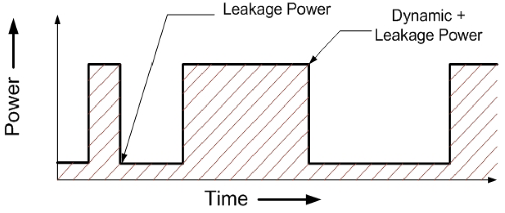
Figure 3 shows the total power dissipation of a single representative pipeline stage in one component. Note that the total power reduces to just the leakage part in the absence of a valid instruction in that stage (
idle), and the average dynamic power of the stage is added when an instruction is processed (
active).
Figure 3.
Power Dissipation transient for a single pipeline stage in a component. The area under the curve is the total Energy consumption.
Figure 3.
Power Dissipation transient for a single pipeline stage in a component. The area under the curve is the total Energy consumption.
A certain pipeline stage of a component will switch to active state when it receives an instruction ready signal from its previous stage. In the absence of the instruction ready signal, the stage switches back to idle state. Note that the instruction ready signal is used to clock-gate (disable the clock to all logic of) an entire component or a single pipeline stage inside the component to save dynamic power. Hence we only consider leakage power dissipation in the absence of an active instruction. In case of an instruction waiting for memory access or in the stall state due to a prior long latency operation, is assumed to be in active state.
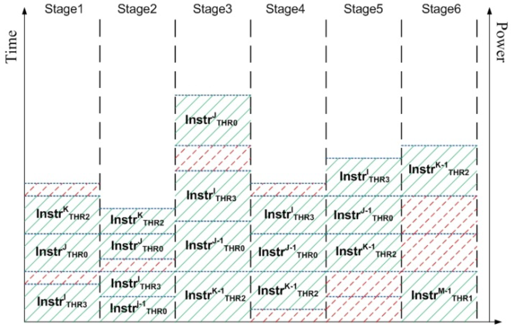
Figure 4 illustrates the methodology of power measurement in the pipelined components in CASPER as seen during 5 clock cycles. The blue dotted lines show the amount of power dissipated by the pipeline stage as an instruction from a particular hardware thread is executed. Time increases vertically. For example, for the 5 clock cycles as shown in
Figure 4 the total contribution of Stage1 is given by
The shaded parts correspond to active states of the stage (dynamic + leakage power), while the dotted parts correspond to idle states of the stage (only leakage power). Note that different stages have different values of dynamic and leakage power dissipations.
Figure 4.
Power profile of a pipelined component where multiple instructions exist in different stages. Dotted parts of the pipeline are in idle state and add to the leakage power dissipation. Shaded parts of the pipeline are active and contribute towards both dynamic and leakage power dissipations.
2.3. Power Dissipation Modeling of L2 Cache and Interconnection Network
The power and area of L2 cache and interconnection network however depend on the number of cores which makes it immensely time-consuming to synthesize, place and route all possible combinations. Hence we have used
multiple linear regression [
28] for this purpose. The training set required to derive the regression models of dynamic power and area of L2 cache arrays are measured by running Cacti 4.0 [
27] for different configurations of L2 cache size, associativity and line sizes. Dynamic power dissipation measured in Watts of L2 cache is related to the size in megabytes, associativity and number of banks
NB as shown in Equation 2. The error of estimate found for this model ranges between 0.524 and 2.09. Errors are estimated by comparing the model predicted and measure value of dynamic power dissipation for configurations of L2 cache size, associativity, linesize and number of banks. These configurations are different from the ones used to derive the training set.
Similarly, the dynamic and leakage power dissipation measured in mill watts of a crossbar interconnection network is given by Equation 3 and Equation 4 respectively. The training set required to derive the regression models of dynamic and leakage power of the crossbar are derived by synthesizing its hardware model parameterized in terms of number of L2 cache banks and number of cores using Synopsys Design Vision and Cadence Encounter. Note that dynamic and leakage power is related square of the number of cores (
NC) and number of cache banks (
NB) which means that the power dissipation scales super linearly with number of banks and cores. Thus, crossbar interconnects are not scalable. However, they provide high bandwidth required in our many-core designs. The regression model parameters and 95% confidence interval as reported by the statistical tool SPSS [
29] are for dynamic and leakage power dissipation is shown in
Table 4 and
Table 5 respectively. The confidence interval shows that the strength of the model is high. The models are further validated by comparing the model predicted power values and values measured by synthesizing 5 more combinations of number of L2 cache banks and number of cores different from the training set. We found that in these two cases, the errors of estimates ranges between 0.7 and 10.64.
Table 4.
Regression model parameters of dynamic power of interconnection network.
Table 4.
Regression model parameters of dynamic power of interconnection network.
| | | 95% Confidence Interval |
|---|
| Parameter | Standard Error | Lower Bound | Upper Bound |
|---|
| b0 | 0.003 | 0.191 | 0.203 |
| b1 | 0.198 | 1.628 | 2.501 |
Table 5.
Regression model parameters of leakage power of interconnection network.
Table 5.
Regression model parameters of leakage power of interconnection network.
| | | 95% Confidence Interval |
|---|
| Parameter | Standard Error | Lower Bound | Upper Bound |
|---|
| b0 | 0.001 | 0.016 | 0.017 |
| b1 | 0.018 | 0.180 | 0.255 |
2.4. Hardware Controlled Power Management in CASPER
Two hardware-controlled power management algorithms called Chipwide DVFS and MaxBIPS as proposed in [
30] are implemented in CASPER. Note that all these algorithms continuously re-evaluate the voltage-frequency operating levels of the different cores, once every evaluation cycle. When not explicitly stated, one evaluation cycle corresponds to 1024 processor clock cycles in our simulations. The DVFS based GPMU algorithms rely on the assumption that when a given core switches from power mode
A (voltage_
A, frequency_
A) in time interval
N to power mode
B (voltage_
B, frequency_
B) in time interval
N + 1, the power and throughput in time interval
N + 1 can be predicted using Equation (1). Note that the system frequency needs to scale along with the voltage to ensure that the operating frequency meets the timing constraints of the circuit whose delay changes linearly with the operating voltage [
31]. This assumes that the workload characteristics do not change from one time interval to next one, and there are no shared resource dependencies between tasks and cores.
Table 6 explains the dependencies of power and throughput on the voltage and frequency levels of the cores.
Table 6.
Relationship of power and throughput in time interval N and N + 1.
Table 6.
Relationship of power and throughput in time interval N and N + 1.
| Time Interval | N | N + 1 |
|---|
| Mode | (v, f) | (v’, f’) |
| f’ = f (v’/v) |
| Throughput | T | T’ = T ×
(f’/f) |
| Dynamic Power | P | P’ = P × (v’/v)2 × (f’/f) |
The key idea of DVFS in Chipwide DVFS is to scale the voltages and frequencies of a single core or the entire processor during run-time to achieve specific throughputs while minimizing power dissipation, or to maximize throughput under a power budget. Equation (5) shows the quadratic and linear dependences of dynamic or switching power dissipation on the supply voltage and frequency respectively:
where
α is the switching probability, C is the total transistor gate (or sink) capacitance of the entire module,
Vdd is the supply voltage, and
f is the clock frequency. Note that the system frequency needs to scale along with the voltage to satisfy the timing constraints of the circuit whose delay changes linearly with the operating voltage [
30]. DVFS algorithms can be implemented at different levels such as the processor micro-architecture (hardware), the operating system scheduler, or the compiler [
32].
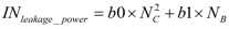
Figure 5 shows a conceptual diagram implementing DVFS on a multi-core processor. Darker shaded regions represent cores operating at high voltage, while lighter shaded regions represent cores operating at low voltage. The unshaded cores are in sleep mode.
Figure 5.
Dynamic voltage and frequency scaling (DVFS) for a multi-core processor.
Figure 5.
Dynamic voltage and frequency scaling (DVFS) for a multi-core processor.
Chipwide DVFS is a global power management scheme that monitors the entire chip power consumption and performance, and enforces a uniform voltage-frequency operating point for all cores to minimize power dissipation under an overall throughput budget. This approach does not need any individual information about the power and performance of each core, and simply relies on entire chip throughput measurements to make power mode switching decisions. As a result, one high performance core can push the entire chip over throughput budget, thereby triggering DVFS to occur across all cores on-chip. A scaling down of voltage and frequency in cores which are not exceeding their throughput budgets will further reduce their throughputs. This may be undesirable, especially if these cores are running threads from different applications which run at different performance levels. The pseudo-code is shown in
Table 7. Cumulative power dissipation is calculated by adding the power dissipation observed in the last evaluation cycle to the total power dissipation of
Corei from time
T = 0. Cumulative throughput similarly is the total number of instructions committed until now from time
T = 0 including the instructions committed in the last evaluation cycle. Also, in this case the current core DVFS level is same across all the cores.
Table 7.
Pseudo Code of Chipwide DVFS.
Table 7.
Pseudo Code of Chipwide DVFS.
| /* this algorithm continuously executes once every evaluation cycle */ |
| Get_current_core_dvfs_level; |
| For all Coresi { |
| Get power dissipated by Corei in the last evaluation cycle; |
| Get effective throughput of
Corei in the last evaluation cycle; |
| Sum up cumulative power dissipated by all cores in the last evaluation cycle; |
| Sum up cumulative throughput of all cores in the last evaluation cycle; |
| } |
| If (Overall throughput of all cores > throughput budget) { |
| if (current_core_dvfs_level > lowest_dvfs_level) { |
| Lower down current_core_dvfs_level to next level; |
| } |
| } |
| For all Coresi { |
| Update every core’s new dvfs level; |
| } |
The MaxBIPS algorithm [
30] monitors the power consumption and performance at the global level and collects information about the entire chip throughput, as well as the throughput contributions of individual cores. The power mode for each core is then selected so as to minimize the power dissipation of the entire chip, while maximizing the system performance subject to the given throughput budget. The algorithm evaluates all the possible combinations of power modes for each core, and then chooses the one that minimizes the overall power dissipation and maximizes the overall system performance while meeting the throughput budget by examining all voltage/frequency pairs for each core. The cores are permitted to operate at different voltages and frequencies in MaxBIPS algorithm. A linear scaling of frequency with voltage is assumed in MaxBIPS [
30].
Based on
Table 6, the MaxBIPS algorithm predicts the estimated power and throughput for all possible combinations of cores and voltage/frequency modes (
vf_mode) or scaling factors and selects the (core_
i,
vf_mode_
j) that minimizes power dissipation, but maximizes throughput while meeting the required throughput budget. The pseudo-core of MaxBIPS algorithm is shown in
Table 8, the
Power Mode Combinationi used in MaxBIPS algorithm is a lookup table storing all the possible combinations of DVFS levels across the cores. For example, if there are 4 cores and 3 DVFS levels as described in
Table 6 which stores the predicted power consumption and throughput observed until the last evaluation cycle in the chip for all possible combinations of DVFS levels across the cores in the chip.
Table 8.
Pseudo-code of MaxBIPS DVFS.
Table 8.
Pseudo-code of MaxBIPS DVFS.
| /* this algorithm continuously executes once every evaluation cycle */ |
| Define_power_mode_combinations; |
| Initialize Min_power; |
| Initialize Max_throughput; |
| Initialize Selected_combination; |
| --voltage frequency (power mode) combinations for different cores |
| For all Coresi { |
| dvfsLevel = Get current DVFS level of Corei; |
| Get power dissipated by Corei in the last evaluation cycle; |
| Get effective throughput of Corei in the last evaluation cycle; |
| } |
| For all Power_Mode_Combinationsj { |
| For all Coresk { |
| Calculate predicted throughput value of core k in combination_j; |
| --Using power_mode_combination, Equation (2) |
| Calculate predicted power value of core k in combination_j; |
| --Using power_mode_combinations, Equation (2) |
| Accumulate predicted throughputs of all cores in combination_j; |
| Accumulate predicted power dissipations of all cores in combination_j; |
| } |
| If (overall_predicted_throughput of all cores <= throughput budget) { |
| If (Max_throughput < overall_predicted_throughput of all cores) { |
| Max_throughput = overall_predicted_throughput of all cores; |
| Min_power = overall_predicted_power of all cores; |
| Selected_combination = j; |
| } |
| If (Max_throughput = overall_predicted_throughput of all cores) { |
| Max_throughput = overall_predicted_throughput of all cores; |
| If (Min_power >= overall_predicted_power of all cores) |
| Min_power = overall_predicted_power of all cores; |
| Selected_combination = j; |
| } |
| } |
| } |
| For all Coresi { |
| Update every core’s new dvfs level with values in Selected_combination; |
| } |
The three DVFS levels used in Chipwide DVFS and MaxBIPS DPM are shown in
Table 9. These voltage-frequency pairs have been verified using the experimental setup of
Section 4. Note that performance predictions of the existing GPMU algorithms to be discussed this section do not consider the bottlenecks caused by shared memory access between cores.Please note that all synchronization between the cores is resolved in the L2 cache. During the cycle-accurate simulation, the L2 cache accesses from the cores are resolved using arbitration logic and queues in the L2 cache controllers. In case of L1 cache misses, packets are sent to the L2 cache which brings the data back in as load misses. An increased L1 cache miss hence means longer wait time for the instruction which caused the miss and effectively we observe the cycles per instruction (CPI) of the core to decrease.
Table 9.
DVFS Levels used in Chipwide DVFS and MaxBIPS.
Table 9.
DVFS Levels used in Chipwide DVFS and MaxBIPS.
| DVFS Level ID | Voltage-Frequency Combination |
|---|
| DVFS_LEVEL_0 | 0.85 V, 0.85 GHz |
| DVFS_LEVEL_1 | 1.7 V, 1.7 GHz |
| DVFS_LEVEL_2 | 1.7 V, 3.4 GHz |
3. Embedded Processor Benchmark (ENePBench)
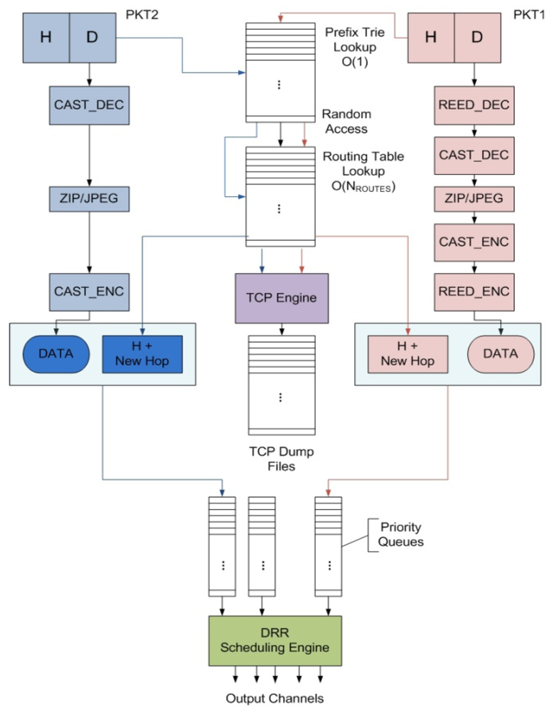
Figure 6.
Pictorial representation of IP packet header and payload processing in two packet instances of different types.
Figure 6.
Pictorial representation of IP packet header and payload processing in two packet instances of different types.
To evaluate the performance and power dissipation of candidate designs we have developed a benchmark suite called
Embedded Network Packet Processing Benchmark (ENePBench) which emulates the IP packet processing tasks executed in a network router. The router workload varies according to internet usage where random number of IP packets arrive at random intervals. To meet a target bandwidth, the router has to: (i) process a required number of packets per second; and (ii) process individual packets within their latency constraints. The task flow is described in
Figure 6. Incoming IPv6 packets are scheduled on the processing cores of the NeP based on respective packet types and priorities. Depending on the type of a packet different header and payload processing functions process the header and payload of the packet respectively. Processed packets are either routed towards the outward queues (in case of pass-through packets) or else terminated.
The packet processing functions of ENePBench are adapted from CommBench 0.5 [
33]. Routing table lookup function RTR, packet fragmentation function FRAG and traffic monitoring function TCP constitute the packet header functions. Packet payload processing functions include encryption (CAST), error detection (REED) and JPEG encoding and decoding as shown in
Table 10.
Table 10.
Packet processing functions in ENePBench.
Table 10.
Packet processing functions in ENePBench.
| Function Type | Function Name | Description |
|---|
| Header Processing Functions | RTR | A Radix-Tree routing table lookup program |
| FRAG | An IP packet fragmentation code |
| TCP | A traffic monitoring application |
| Payload Processing Functions | CAST | A 128 bit block cipher algorithm |
| REED | An implementation of Reed-Solomon Forward Error Correction scheme |
| JPEG | A lossy image data compression algorithm |
| Packet Scheduler | DRR | Deficit Round Robin fair scheduling algorithm |
Functionally, IP packets are further classified into types TYPE0 to TYPE4 as shown in
Table 11. The headers of all packets belonging to packet types TYPE0 to TYPE4 are used to lookup the IP routing table (RTR), managing packet fragmentation (FRAG) and traffic monitoring (TCP). The payload processing of the packet types, however, is different from each other. Packet types TYPE0, TYPE1 and TYPE2 are compute bound packets and are processed with encryption and error detection functions. In case of packet type TYPE3 and TYPE4, the packet payloads are processed with both compute bound encryption and error detection functions as well as data bound JPEG encoding/decoding functions.
Table 11.
Packet Types used in ENePBench.
Table 11.
Packet Types used in ENePBench.
| Packet Type | Header Functions | Data Functions | Characteristic | Type of Service |
|---|
| TYPE0 | RTR, FRAG, TCP | REED | Compute Bound | Real Time |
| TYPE1 | RTR, FRAG, TCP | CAST | Compute Bound | Real Time |
| TYPE2 | RTR, FRAG, TCP | CAST, REED | Compute Bound | Content-Delivery |
| TYPE3 | RTR, FRAG, TCP | REED, JPEG | Data Bound | Content-Delivery |
| TYPE4 | RTR, FRAG, TCP | CAST, REED, JPEG | Data Bound | Content-Delivery |
The two broad categories of IP Packets are hard real-time termed as
real-time packets and soft real-time termed as
content-delivery packets.
Real-time packets are assigned with high priority whereas
content-delivery packets are processed with lower priorities.
Table 12 enlists the end-to-end transmission delays associated with each packet categories [
34]. The total propagation delay (source to destination) of
real-time packets is less than 150 milliseconds (ms) and less than 10 s for
content-delivery packets respectively [
34].
Table 12.
Performance Targets for IP packet type.
Table 12.
Performance Targets for IP packet type.
| Application/Packet Type | Data Rate | Size | End-to-end Delay | Description |
|---|
| Audio | 4–64 (KB/s) | <1 KB | <150 ms | Conversational Audio |
| Video | 16–384 (KB/s) | ~10 KB | <150 ms | Interactive video |
| Data | - | ~10 KB | <250 ms | Bulk data |
| Still Image | - | <100 KB | <10 s | Images/Movie clips |
In practice 10 to 15 hops are allowed per packet which means the
worst case processing time is approximately 10 ms in case of real-time packets and 1000 ms in case of content-delivery packets respectively [
34] per intermediate router. For each packet the
worst case processing time in a router includes the wait time in incoming packet queue, packet header and payload processing time and wait time in the output queues [
35]. Traditionally schedulers in NePs snoop on the incoming packet queues and upon packet arrival generate
interrupts to the processing cores. A
context switch mechanism is subsequently used to dispatch packets to the individual cores for further processing. Current systems however use a switching mechanism to directly move packets from incoming packet queues to the cores avoiding expensive signal interrupts [
36]. Hence, in our case we have not considered interrupt generation and context switch time to calculate
worst case processing time. Also due to the low propagation time in current high bandwidth optical fiber networks we ignore the propagation time of packets through the network wires [
37]. In our methodology the individual cores are designed such that they are able to process packets within the
worst case processing time.
5. Results
The power dissipation and throughput observed by varying the key micro-architectural components namely number of threads per core, data and instruction cache sizes per core, store buffer size per thread in a core and number of cores in the chip are showed in
Figure 7 to
Figure 21. Note that Hardware Power Management is not enabled for the experiments generating data shown for
Figure 7 through
Figure 21. In each of the figures, power-performance trade-offs are shown by co-varying two micro-architectural parameters while the other parameters are kept at a constant value as described in the baseline architecture shown in
Table 14. Cycles per instruction per core or CPI-per-core (lower is better) is measured by the total number of clock cycles during the runtime of a workload divided by the total number of committed instructions across all the hardware threads during that time and average cycles per instruction per thread or CPI-per-thread is measured by the number of clock cycles divided by the number of instructions committed in a hardware thread during the same time. All the data is based on the execution of compute bound packet type 1 (TYPE1) as described in
Table 11.
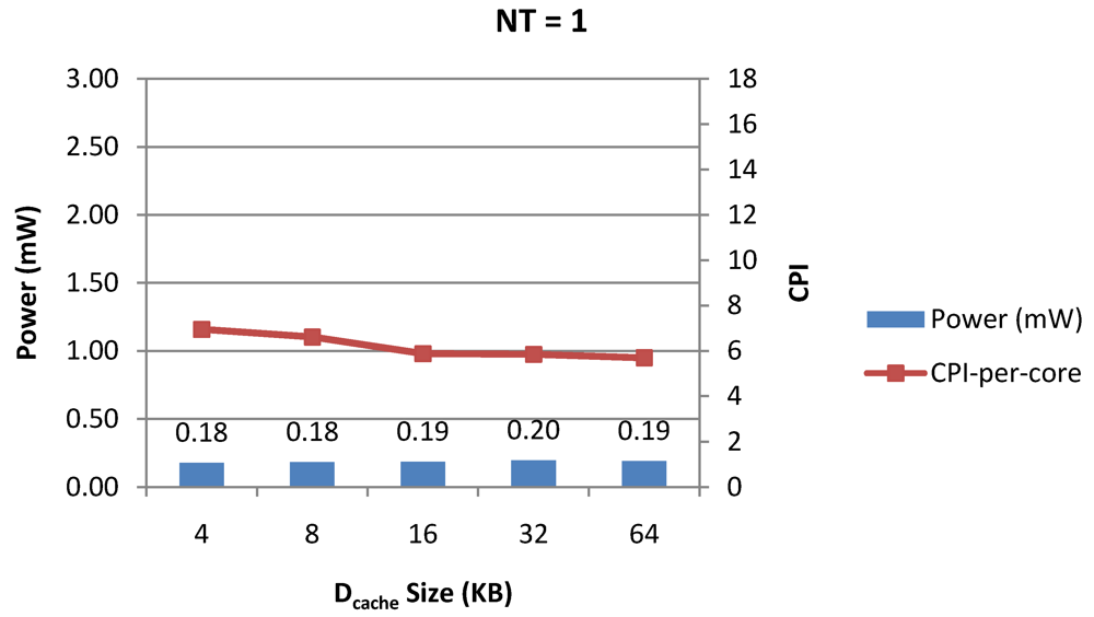
Figure 7.
Power dissipation versus CPI-per-thread in a 1-core 1-thread 1 MB L2 cache processor where the data cache size is varied from 4 KB to 64 KB for packet type TYPE1.
Figure 7.
Power dissipation versus CPI-per-thread in a 1-core 1-thread 1 MB L2 cache processor where the data cache size is varied from 4 KB to 64 KB for packet type TYPE1.
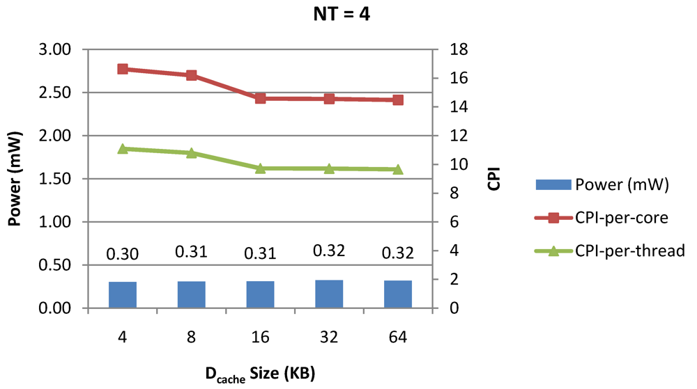
Figure 8.
Power dissipation, CPI-per-core and CPI-per-thread in a 1-core 4-thread 1 MB L2 cache processor where the data cache size is varied from 4 KB to 64 KB for packet type TYPE1.
Figure 8.
Power dissipation, CPI-per-core and CPI-per-thread in a 1-core 4-thread 1 MB L2 cache processor where the data cache size is varied from 4 KB to 64 KB for packet type TYPE1.
Figure 9.
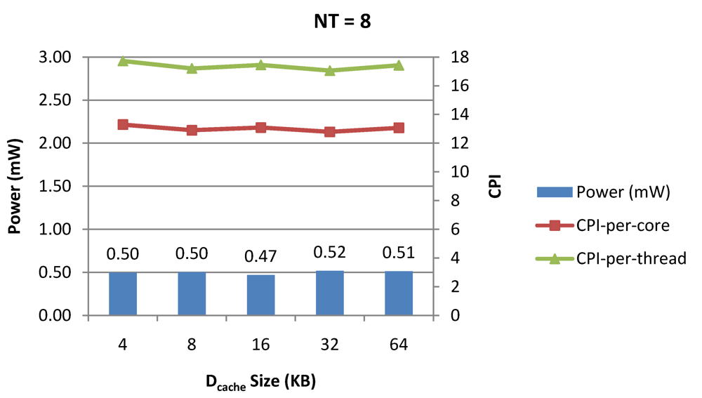
Power dissipation, CPI-per-core and CPI-per-thread in a 1-core 8-thread 1 MB L2 cache processor where the data cache size is varied from 4 KB to 64 KB for packet type TYPE1.
Figure 9.
Power dissipation, CPI-per-core and CPI-per-thread in a 1-core 8-thread 1 MB L2 cache processor where the data cache size is varied from 4 KB to 64 KB for packet type TYPE1.
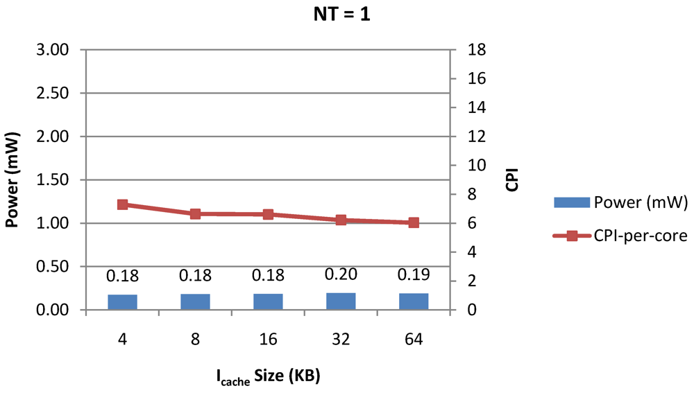
Figure 10.
Power dissipation, CPI-per-core and CPI-per-thread in a 1-core 1-thread 1 MB L2 cache processor where the instruction cache size is varied from 4 KB to 64 KB for packet type TYPE1.
Figure 10.
Power dissipation, CPI-per-core and CPI-per-thread in a 1-core 1-thread 1 MB L2 cache processor where the instruction cache size is varied from 4 KB to 64 KB for packet type TYPE1.
Figure 11.
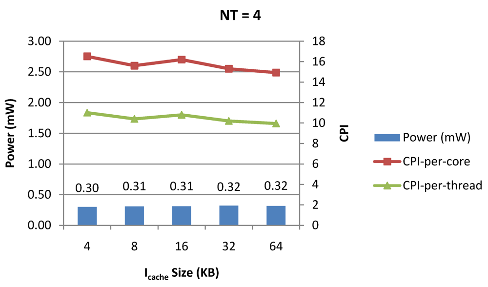
Power dissipation, CPI-per-core and CPI-per-thread in a 1-core 4-thread 1 MB L2 cache processor where the instruction cache size is varied from 4 KB to 64 KB for packet type TYPE1.
Figure 11.
Power dissipation, CPI-per-core and CPI-per-thread in a 1-core 4-thread 1 MB L2 cache processor where the instruction cache size is varied from 4 KB to 64 KB for packet type TYPE1.
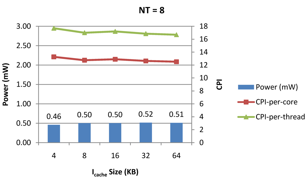
Figure 12.
Power dissipation, CPI-per-core and CPI-per-thread in a 1-core 8-thread 1 MB L2 cache processor where the instruction cache size is varied from 4 KB to 64 KB for packet type TYPE1.
Figure 12.
Power dissipation, CPI-per-core and CPI-per-thread in a 1-core 8-thread 1 MB L2 cache processor where the instruction cache size is varied from 4 KB to 64 KB for packet type TYPE1.
Figure 13.
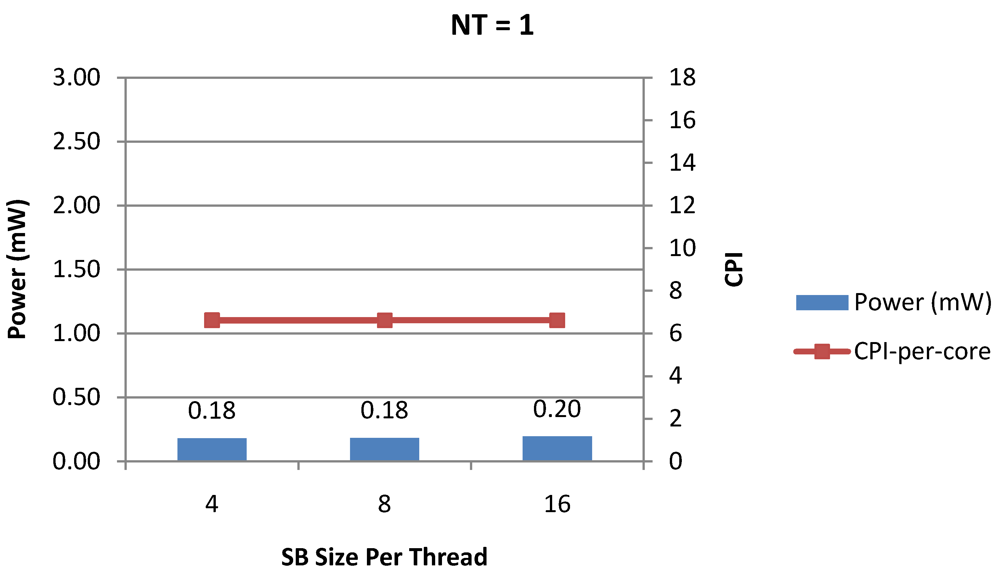
Power dissipation and CPI-per-core in a 1-core 1-thread 1 MB L2 cache processor where the store buffer size is varied from 4 to 16 for packet type TYPE1.
Figure 13.
Power dissipation and CPI-per-core in a 1-core 1-thread 1 MB L2 cache processor where the store buffer size is varied from 4 to 16 for packet type TYPE1.
Figure 14.
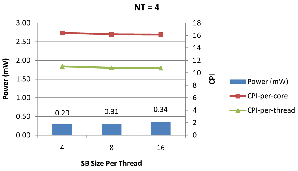
Power dissipation, CPI-per-core and CPI-per-thread in a 1-core 4-thread 1 MB L2 cache processor where the store buffer size is varied from 4 to 16 for packet type TYPE1.
Figure 14.
Power dissipation, CPI-per-core and CPI-per-thread in a 1-core 4-thread 1 MB L2 cache processor where the store buffer size is varied from 4 to 16 for packet type TYPE1.
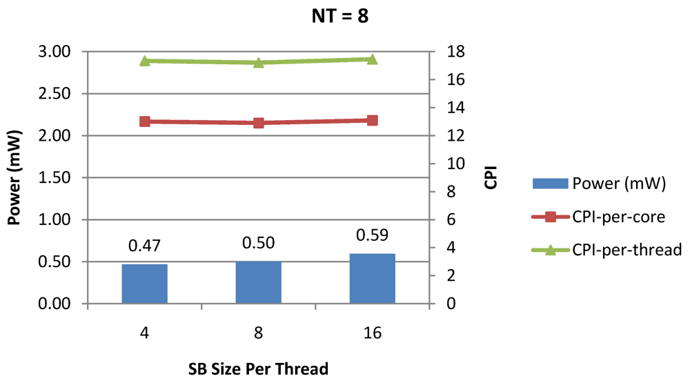
Figure 15.
Power dissipation, CPI-per-core and CPI-per-thread in a 1-core 8-thread 1 MB L2 cache processor where the store buffer size is varied from 4 to 16 for packet type TYPE1.
Figure 15.
Power dissipation, CPI-per-core and CPI-per-thread in a 1-core 8-thread 1 MB L2 cache processor where the store buffer size is varied from 4 to 16 for packet type TYPE1.
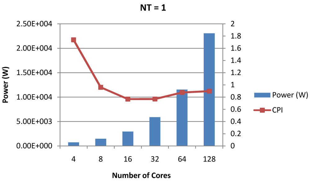
Figure 16.
Power dissipation and overall CPI trade-offs as number of cores is scaled from 4 to 128. All the cores have NT = 1 for packet type TYPE1.
Figure 16.
Power dissipation and overall CPI trade-offs as number of cores is scaled from 4 to 128. All the cores have NT = 1 for packet type TYPE1.
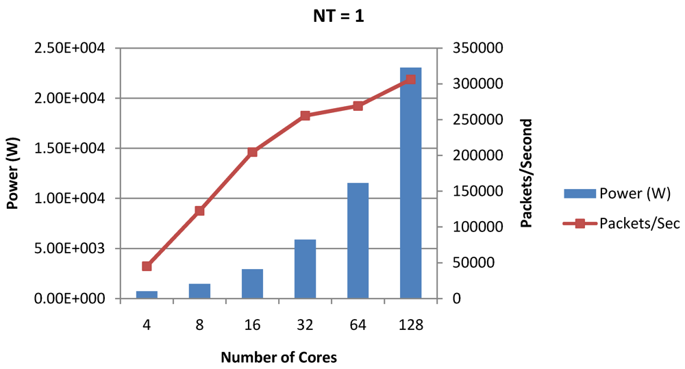
Figure 17.
Power dissipation and packet bandwidth as number of cores is scaled from 4 to 128. All the cores have NT = 1 for packet type TYPE1.
Figure 17.
Power dissipation and packet bandwidth as number of cores is scaled from 4 to 128. All the cores have NT = 1 for packet type TYPE1.
Figure 18.
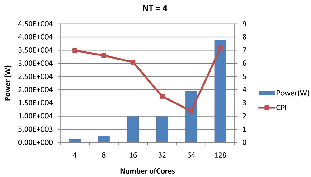
Power dissipation and CPI as number of cores is scaled from 4 to 128. All the cores have NT = 4 for packet type TYPE1.
Figure 18.
Power dissipation and CPI as number of cores is scaled from 4 to 128. All the cores have NT = 4 for packet type TYPE1.
Figure 19.
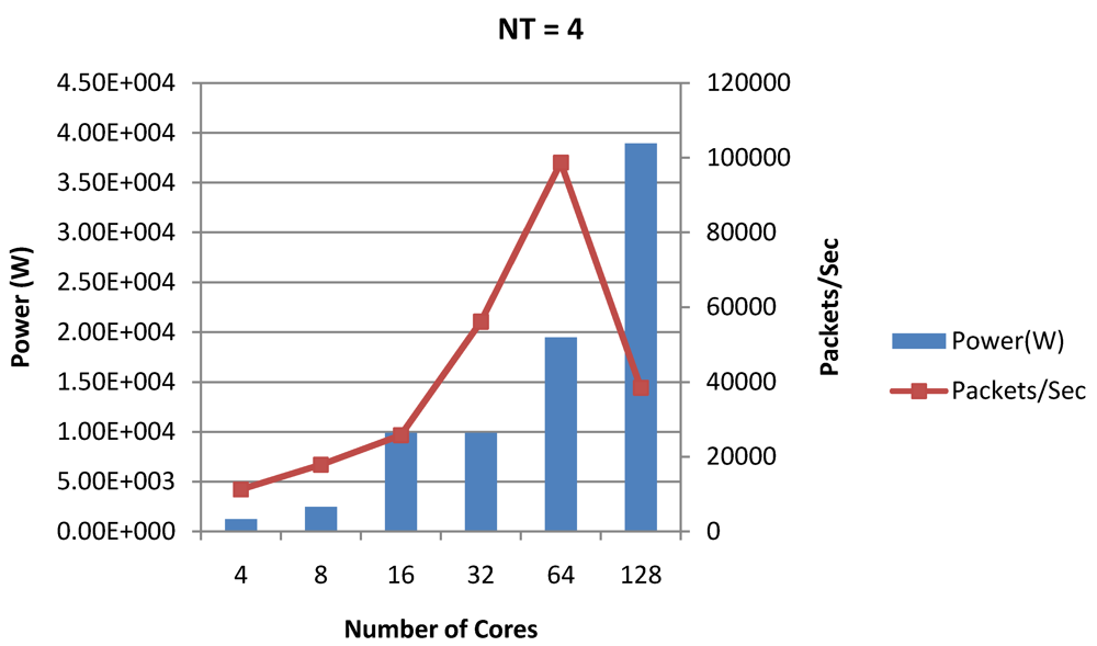
Power dissipation and packet bandwidth as number of cores is scaled from 4 to 128. All the cores have NT = 4 for packet type TYPE1.
Figure 19.
Power dissipation and packet bandwidth as number of cores is scaled from 4 to 128. All the cores have NT = 4 for packet type TYPE1.
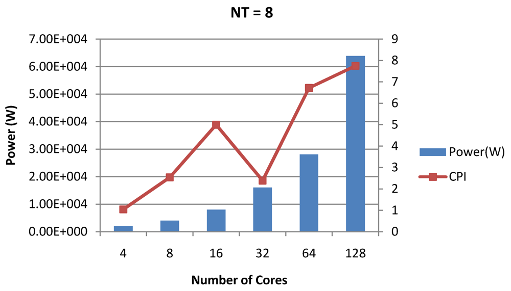
Figure 20.
Power dissipation and CPI as number of cores is scaled from 4 to 128. All the cores have NT = 8 for packet type TYPE1.
Figure 20.
Power dissipation and CPI as number of cores is scaled from 4 to 128. All the cores have NT = 8 for packet type TYPE1.
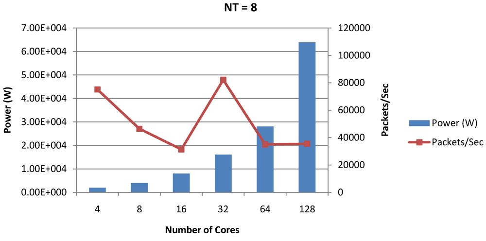
Figure 21.
Power dissipation and packet bandwidth as number of cores is scaled from 4 to 128. All the cores have NT = 8 for packet type TYPE1.
Figure 21.
Power dissipation and packet bandwidth as number of cores is scaled from 4 to 128. All the cores have NT = 8 for packet type TYPE1.
Table 14.
Baseline architecture for packet type TYPE1 to study the power-performance trade-offs in single-core designs.
Table 14.
Baseline architecture for packet type TYPE1 to study the power-performance trade-offs in single-core designs.
| Field | Value |
|---|
| Number of threads | 4 |
| Data cache size | 8 KB |
| Data cache associativity | 4 |
| Data cache line size | 32 |
| Instruction cache size | 16 KB |
| Instruction cache associativity | 4 |
| Instruction cache line size | 32 |
| Store Buffer size | 4 |
| Load Miss Queue size | 4 |
| ASI Queue size | 2 |
| L2 cache size | 4 MB |
| L2 cache banks | 4 |
| L2 cache associativity | 16 |
| L2 cache line size | 64 |
Figure 7,
Figure 8 and
Figure 9 show the power dissipation, CPI-per-core and average CPI-per-thread for
NT = 1, 4 and 8 respectively as data cache size is scaled from 4 KB to 64 KB. In
Figure 7, the increase in D$ size reduces the data miss rate and hence both CPI-per-thread and CPI-per-core improve. Power dissipation however increases due to increasing D$ size. The figures also demonstrates the trade-offs between performance and power when number of threads is scaled from 1 to 8. The increase in the number of threads in a core means performance of individual threads is slowed down by as many cycles as the number of threads due to the round robin small latency thread scheduling scheme. CPI-per-core however is not linearly dependent on the number of threads. While factors such as increased cache sharing, increased pipeline sharing, lesser pipeline stalls improves CPI-per-core with thread-scaling, factors such as increased stall time at the store buffer, instruction miss queue and load miss queues tend to diminish it. Hence, we clearly see a non-linear pattern where CPI-per-core is higher in
NT = 4 compared to
NT = 8. In case of
NT = 8, we observe 10% decrease in cache misses which results in lower CPI-pe-core compared to
NT = 4. However, this is not the case when
NT is increased from 1 to 4. Important to note that this behavior is application specific and hence reestablishes the non-linear co-dependencies between performance and the structure and behavior of the micro-architectural components.
Figure 10,
Figure 11 and
Figure 12 show the power dissipation, CPI-per-core and average CPI-per-thread for
NT = 1, 4 and 8 respectively as instruction cache size is scaled from 4 KB to 64 KB. Here also, CPI-per-thread and CPI-per-core improves with increasing I$ size as instruction misses decrease. Power dissipation however increases due to increasing I$ size.
Figure 13,
Figure 14 and
Figure 15 show the power dissipation, CPI-per-core and average CPI-per-thread for store buffer sizes of 4 to 16 for
NT = 1, 4 and 8 respectively. We observe similar increasing power consumption with increasing store buffer size. Both CPI-per-core and CPI-per-strand improve. In all these figures, the co-variance of core-level micro-architectural parameters D$ size, I$ size and SB size articulately demonstrates both the diminishing and positive effects of
NT scaling. Power dissipation increases with
NT. CPI-per-strand increases prohibitively affecting single thread performance due to shared pipeline, whereas CPI-per-core decreases showing improvement in throughput in a core as more instructions are executed in a core due to latency hiding.
Figure 16,
Figure 18 and
Figure 20 show the power dissipation and overall CPI observed in case of
NT = 1, 4 and 8 respectively.
Figure 17,
Figure 19 and
Figure 21 shows the peak power dissipation
versus overall packet bandwidth observed in case of
NT = 1, 4 and 8 respectively. Unlike the figures reporting core-level power dissipation and throughput, the overall power dissipation observed in the following figures include the cycle-accurate dynamic power consumption of the entire chip including all the cores, L2 cache and the crossbar interconnection. Interestingly, despite the consistent increase of peak power dissipation with increasing number of cores in the chip, packet bandwidth does not scale with number of cores due to the contention in the shared L2 cache. The diminishing effects of non-optimality can be observed especially in case of 128 cores. Packet bandwidth non-intuitively decreases as number of cores is scaled from 64 to 128. This further emphasizes the critical need of efficient and scalable micro-architectural power-aware design space exploration algorithms able to scan a wide range of possible design choices and find the optimal power-performance balance. In our case 32 cores is observed to be the optimal design since it shows the best power-performance balance. As shown in
Figure 20, for the packet type TYPE1, with threads per core = 8, we observed both cache misses and pipeline stall reduce minimizing the CPI per core. In addition, with number of cores = 32, the wait time in the L2 cache queues was also minimum compared to the other core counts. Hence, in our case study of packet type TYP1, we found that with
NT = 8, the optimal number of cores was 32. Increasing number of cores is diminishingly affecting throughput due to the non-optimal L2 cache micro-architecture which is divided into only 4 banks. Altering the number of L2 cache banks will mitigate contention and help increase packet bandwidth.
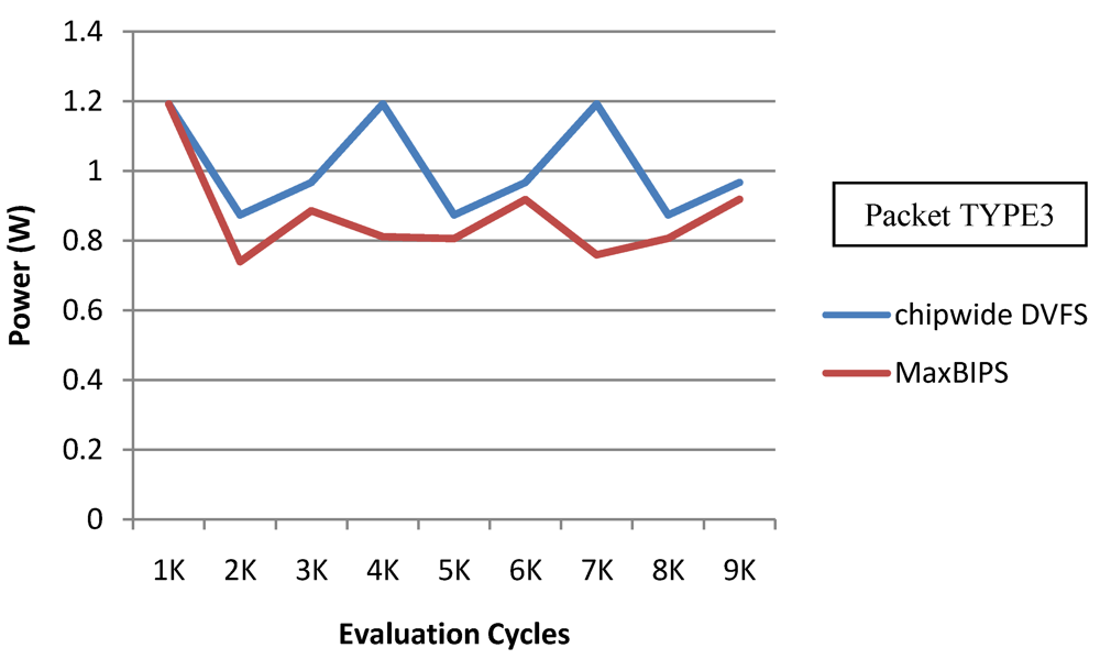
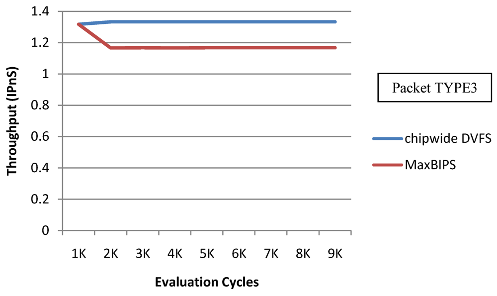
In
Figure 22 and
Figure 23, we show the power and throughput data (with a throughput budget constrained to at 90% of peak throughput with any voltage and frequency scaling) for Chipwide DVFS and MaxBIPS policies for packet type 3 (TYPE3) which is a typical representative of all other packet types. The baseline architecture is displayed in
Table 15. Values on the X-axis correspond to the number of evaluation cycles, where one evaluation cycle is the time period between consecutive runs of the power management algorithms. Where not explicitly stated, one evaluation cycle corresponds to 1024 processor clock cycles in our simulations. In
Figure 22, the X-axis represents number of clock cycles and the Y-axis represents power (W). In
Figure 23, the Y-axis represents throughput (in instructions per nanosecond-IPnS).
Figure 22.
Power for Chipwide DVFS and MaxBIPS.
Figure 22.
Power for Chipwide DVFS and MaxBIPS.
Figure 23.
Throughput for Chipwide DVFS and MaxBIPS.
Figure 23.
Throughput for Chipwide DVFS and MaxBIPS.
Table 15.
Baseline architecture used in the experiments for power management.
Table 15.
Baseline architecture used in the experiments for power management.
| Fields | Value |
|---|
| Number of threads | 4 |
| Data cache size | 8 KB |
| Data cache associativity | 4 |
| Data cache line size | 32 |
| Instruction cache size | 16 KB |
| Instruction cache associativity | 4 |
| Instruction cache line size | 32 |
| Store Buffer size | 4 |
| Load Miss Queue size | 4 |
| ASI Queue size | 2 |
| Number of Cores | 4 |
| L2 cache size | 4 MB |
| L2 cache banks | 4 |
| L2 cache associativity | 16 |
| L2 cache line size | 64 |
As
Figure 22 shows, the power consumption of MaxBIPS is much higher than Chipwide DVFS (the latter being the lower in power dissipation among the two methods). However the throughput of MaxBIPS is also higher than Chipwide DVFS. The percentage power-saving in all the cores in case of Chipwide DVFS and MaxBIPS is shown in
Table 16.
Table 16.
Percentage power-saving due to Chipwide DVFS and MaxBIPS.
Table 16.
Percentage power-saving due to Chipwide DVFS and MaxBIPS.
| | All Cores Running at 3.4 GHz | Chipwide DVFS | MaxBIPS |
|---|
| Power (W) | 0.0 | 35.9 | 26.2 |
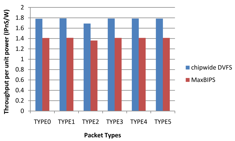
Figure 24 depicts the throughput per unit power (T/P) data for the two methods. Chipwide DVFS has the highest T/P values for the different packet types. Note that high T/P value for Chipwide DVFS arises from the fact that power dissipation in this scheme is substantially lower than other schemes, and not because the throughput is high. When implementing power management by Chipwide DVFS, any increase in the throughput of a single core over a target threshold triggers chipwide operating voltage (and hence, frequency) reductions in all cores, to save power. Hence, once the overall throughput exceeds the budget, all the cores have to adjust their power modes to a lower level. While this method reduces the overall power dissipation substantially, it also leads to excessive performance reductions in all cores as shown in
Figure 24.
Figure 24.
Throughput per unit power data.
Figure 24.
Throughput per unit power data.
A modification of the Chipwide DVFS algorithm required for achieving high performance is to assign a lower bound of throughput.
Figure 25 and
Figure 26 show the power and throughput Chipwide DVFS characteristics (with a lower bound of throughput budget constrained to at 60% of peak throughput with all voltage-frequency levels) for packet type 3 (TYPE3). The power consumption and throughput of Chipwide DVFS are higher than those of MaxBIPS; this can be explained by the fact that the lower bound of throughput does not allow Chipwide DVFS to scale all the cores to lower voltage-frequency levels in order to guarantee the system performance. However the throughput per unit power of Chipwide DVFS is lower than those of MaxBIPS as
Figure 27 demonstrates. The percentage power-saving in case of Chipwide DVFS with and without lower bound on throughput is shown in
Table 17.
Table 18 shows the power, throughput, and throughput per unit power in this case.
Figure 25.
Power for Chipwide DVFS and MaxBIPS with a lower bound of throughput budget = 60% peak throughput.
Figure 25.
Power for Chipwide DVFS and MaxBIPS with a lower bound of throughput budget = 60% peak throughput.
Figure 26.
Throughput for Chipwide DVFS and MaxBIPS with a lower bound of throughput budget = 60% peak throughput.
Figure 26.
Throughput for Chipwide DVFS and MaxBIPS with a lower bound of throughput budget = 60% peak throughput.
Figure 27.
Throughput per unit power data (Chipwide DVFS with lower bound throughput).
Figure 27.
Throughput per unit power data (Chipwide DVFS with lower bound throughput).
Table 17.
Percentage power-saving due to Chipwide DVFS and MaxBIPS.
Table 17.
Percentage power-saving due to Chipwide DVFS and MaxBIPS.
| | All Cores Running at 3.4 GHz | Chipwide DVFS | MaxBIPS |
|---|
| Power (W) | 0.0 | 25.9 | 18.6 |
Table 18.
Power, throughput, throughput per unit power of Chipwide DVFS with and without lower bound on throughput.
Table 18.
Power, throughput, throughput per unit power of Chipwide DVFS with and without lower bound on throughput.
| | With Lower Bound 60% of Peak T | Without Lower Bound of Throughput |
|---|
| Power in one time interval (W) | Throughput in one time interval (IPnS) | Throughput per unit power (IPnS/W) | Power in one time interval (W) | Throughput in one time interval (IPnS) | Throughput per unit power (IPnS/W) |
|---|
| Chipwide DVFS | 0.252 | 0.332 | 1.318 | 0.105 | 0.184 | 1.752 |
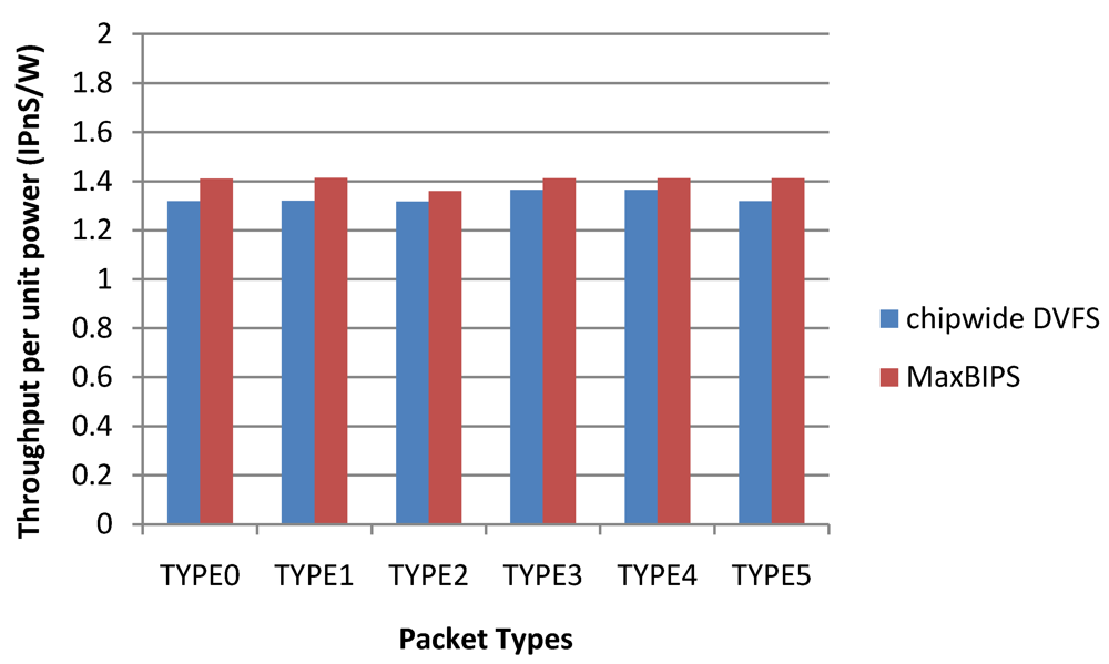
In summary, experimental data show that when Chipwide DVFS is not enabled with lower bound of throughput, MaxBIPS has the highest throughput. Although Chipwide DVFS gives the highest throughput per unit power, its throughput, on average, is lower than that of MaxBIPs, which can be a constraining factor in high throughput systems that require throughputs close to the budget. When Chipwide DVFS is lower-bounded to 60% of peak throughput achievable by Chipwide DVFS, it produces the higher throughput and consumes the higher power between the two methods. This yields the lowest throughput per unit power for Chipwide DVFS, and MaxBIPS saves more power and achieves the highest throughput per unit power compared to the other two policies.
Table 19 shows the relevant experimental results of two policies with different packet types.
Table 19.
Power, throughput, throughput per unit power of two policies for different packet types.
Table 19.
Power, throughput, throughput per unit power of two policies for different packet types.
| | Chipwide DVFS Without Lower Bound | MaxBIPS |
|---|
| P (W) | T (IPnS) | T/P (IPnS/W) | P (W) | T (IPnS) | T/P (IPnS/W) |
|---|
| TYPE0 | 3.72 | 6.61 | 1.78 | 7.53 | 10.62 | 1.41 |
| TYPE1 | 3.72 | 6.65 | 1.79 | 7.54 | 10.65 | 1.41 |
| TYPE2 | 3.93 | 6.65 | 1.69 | 7.83 | 10.65 | 1.36 |
| TYPE3 | 3.72 | 6.64 | 1.78 | 7.54 | 10.64 | 1.41 |
| TYPE4 | 3.72 | 6.64 | 1.78 | 7.54 | 10.63 | 1.41 |
| Average | 3.75 | 6.64 | 1.76 | 7.58 | 10.64 | 1.40 |
Table 20 shows the average power, average throughput, average throughput per unit power, average energy and average latency (execution time) of two power management policies while running about 7300 instructions for all the packet types (averaging is done over all packet types). Results show that on average, Chipwide DVFS consumes 17.7% more energy than MaxBIPS and has 2.34 times its latency.
Table 20.
Average power, average throughput, and average throughput per unit power, average energy, and average execution time of two discussed policies.
Table 20.
Average power, average throughput, and average throughput per unit power, average energy, and average execution time of two discussed policies.
| | P_average (W) | T_average (IPnS) | T/P_average (IPnS/W) | Energy_average (nJ) | Average Latency (nS) |
|---|
| Chipwide without lower bound | 3.75 | 6.64 | 1.77 | 3.371 | 34,816 |
| MaxBIPS | 7.58 | 10.64 | 1.40 | 2.864 | 14,848 |
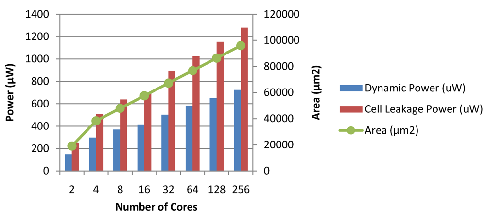
Figure 28 and
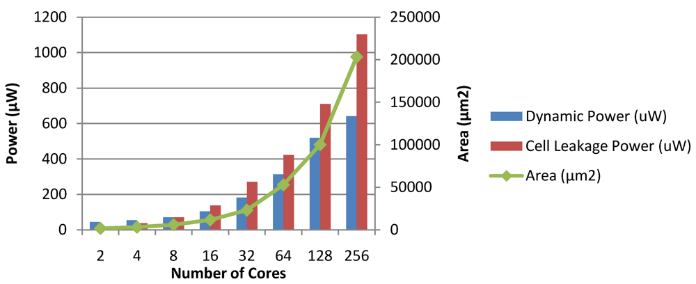
Figure 29 show the dynamic and leakage power dissipations, along with the hardware implementation areas for the Chipwide DVFS and MaxBIPS algorithms, as the number of cores is scaled. The total power dissipation of the MaxBIPS DPM hardware for an 8 core processor is around 101 µW, which is small compared to the average 20% power saving achieved. This justifies the use of on-chip power management units which enable substantial power saving while meeting the performance requirements of the packet processing application.
Figure 28.
Dynamic power, leakage power and area of the Chipwide DVFS module in CASPER.
Figure 28.
Dynamic power, leakage power and area of the Chipwide DVFS module in CASPER.
Figure 29.
Dynamic power, leakage power and area of the MaxBIPS module in CASPER.
Figure 29.
Dynamic power, leakage power and area of the MaxBIPS module in CASPER.
6. Related Work
First we will do a brief survey of existing general purpose processor simulators and then power-aware simulators. The authors of [
15,
38,
39,
40,
41,
42,
43] study variations of power and throughput in heterogeneous architectures. B. C. Lee and D. M. Brooks
et al. minimize the overhead of micro-architectural design space exploration through statistical inference via regression models in [
44]. The models are derived using fast simulations. The work in [
45] differs from these in that they use full-fledged simulations for predicting and comparing performance and power of various architectures. A combination of analytic performance models and simulation-based performance models is used in [
45] to guide design space exploration for sensor nodes. All these techniques rely on efficient processor simulators for architecture characterization.
Virtutech Simics [
46] is a full-system scalable functional simulator for embedded systems. The released versions support microprocessors such as PowerPC, x86, ARM and MIPS. Simics is also capable of simulating any digital device and communication bus. The simulator is able to simulate anything from a simple CPU + memory, to a complex SoC, to a custom board, to a rack of multiple boards, or a network of many computer systems. Simics is empowered with a suite of unique debugging toolset including reverse execution, tracing, fault-injection, checkpointing and other development tools. Similarly, Augmint [
47] is an execution-driven multiprocessor simulator for Intel x86 architectures developed in University of Illinois, Urbana-Champagne. It can simulate uniprocessors as well as multiprocessors. The inflexibility in Augmint arises from the fact that the user needs to modify the source code to customize the simulator to model multiprocessor system. However both Simics and Augmint are not cycle-accurate and they model processors which do not have open-sourced architectures or instruction sets; this limits the potential for their use by the research community. Another execution-driven simulator is RSIM [
48] which models shared-memory multiprocessors that aggressively exploit instruction-level parallelism (ILP). It also models an aggressive coherent memory system and interconnects, including contention at all resources. However throughput intensive applications which exploit task level parallelism are better implemented by the fine-grained multi-threaded cores that our proposed simulation framework models. Moreover we plan to model simple in-order processor pipelines which enable thread schedulers to use small-latency, something vital for meeting real-time constraints.
General Execution-driven Multiprocessor Simulator (GEMS) [
49] is an execution-driven simulator of SPARC-based multiprocessor system. It relies on functional processor simulator Simics and only provides cycle-accurate performance models when potential timing hazards are detected. GEMS Opal provides an out-of-order processor model. GEMS Ruby is a detailed memory system simulator. GEMS Specification Language including Cache Coherence (SLICC) is designed to develop different memory hierarchies and cache coherence models. The advantages of our simulator over the GEMS platform include its ability to (i) carry out full-chip cycle-accurate simulation with guaranteed fidelity which results in high confidence during broad micro-architecture explorations; and (ii) provide
deep chip vision to the architect in terms of chip area requirement and run-time switching characteristics, energy consumption, and chip thermal profile.
SimFlex [
50] is a simulator framework for large-scale multiprocessor systems. It includes (a) Flexus–a full-system simulation platform; and (b) SMARTS–a statistically derived model to reduce simulation time. It employs systematic sampling to measure only a very small portion of the entire application being simulated. A functional model is invoked between measurement periods, greatly speeding the overall simulation but results in a loss of accuracy and flexibility for making fine micro-architectural changes, because any such change necessitates regeneration of statistical functional models. SimFlex also includes FPGA-based co-simulation platform called the ProtoFlex. Our simulator can also be combined with an FPGA based emulation platform in future, but this is beyond the scope of this work.
MPTLsim [
51] is a uop-accurate, cycle-accurate, full-system simulator for multi-core designs based on the X86-64 ISA. MPTLsim extends PTLsim [
52], a publicly available single core simulator, with a host of additional features to support hyperthreading within a core and multiple cores, with detailed models for caches, on-chip interconnections and the memory data flow. MPTLsim incorporates detailed simulation models for cache controllers, interconnections and has built-in implementations of a number of cache coherency protocols. CASPER targets an open-sourced ISA and processor architecture which Sun Microsystems, Inc. has released under the OpenSPARC banner [
4] for the research community.
NePSim2 [
53] is an open source framework for analyzing and optimizing NP design and power dissipation at architecture level. It uses a cycle-accurate simulator for Intel's multi-core IXP2xxx NPs, and incorporates an automatic verification framework for testing and validation, and a power estimation model for measuring the power consumption of the simulated NP. To the best of our knowledge, it is the only NP simulator available to the research community. NePSim2 has been evaluated with cryptographic benchmark applications along with a number of basic test cases. However, the simulator is not readily scalable to explore a wide variety of NP architectures.
Wattch [
17] proposed by David Brooks
et al. is a multi-core micro-architectural power estimation and simulation platform. Wattch enables users to estimate power dissipation of only superscalar out-of-order multi-core micro-architectures. Out-of-order architectures consist of complex structures such as reservation stations, history-based branch predictors, common data-width buses and re-order buffers and hence are not always power-efficient. In case of low-energy processors such as embedded processors and network processors simple in-order processor pipelines are preferred due to their relatively low power consumption. McPAT [
54] proposed by Norman Jouppi is another multi-core micro-architectural power estimation tool. McPAT provides power estimation of both out-of-order and in-order micro-architectures. Although efficient in estimating power dissipation for a wide range of values of the architectural parameters, McPAT is not cycle-accurate and hence incapable of capturing the dynamic interactions between the pipeline stages inside cores and other core-level micro-architectural structures, the shared memory structures and the interconnection network as all cores execute streams of instructions.

