Article

Analysis of Dynamic Differential Swing Limited Logic for Low-Power Secure Applications

ICTEAM institute, Université catholique de Louvain, Place du Levant 3, Louvain-la-Neuve, Belgium
*
Author to whom correspondence should be addressed.
J. Low Power Electron. Appl. 2012, 2(1), 98-126; https://doi.org/10.3390/jlpea2010098
Submission received: 28 December 2011 / Revised: 2 March 2012 / Accepted: 2 March 2012 / Published: 16 March 2012
(This article belongs to the Special Issue Low Power Electronics - Recent Developments)

Abstract

:
Low-power secure applications such as Radio Frequency IDentification (RFID) and smart cards represent extremely constrained environments in terms of power consumption and die area. This paper investigates the power, delay and security performances of the dynamic differential swing limited logic (DDSLL). A complete analysis of an advanced encryption standard (AES) S-box is conducted using a low-power (LP) 65 nm CMOS technology node. Measurements show that the DDSLL S-box has 35% less power consumption than the static CMOS S-box, with an area increase of only 12%, at the expense of a 2.5× increase in delay which remains fairly acceptable for low-power applications such as RFIDs and smart cards. Also when compared to other dynamic differential logic (DDL) styles, simulation results show that DDSLL and dynamic current mode logic (DyCML) consume the same power which is about 1.8× less that of sense amplifier based logic (SABL). The effect of process variations is also studied, measurement results show that the DDSLL style has lower variability in terms of dynamic power as the activity factor (αF ) is deterministic thanks to glitch-free operation. As for security, the perceived information metric demonstrates that the DDSLL S-box has a 3× security margin compared to static CMOS. Therefore, DDSLL presents an interesting tradeoff between improved security and area constrained low-power designs.

1. Introduction

Low-power applications that require a certain amount of security such as passive Radio Frequency IDentification (RFID) and smart cards feature loose constraints in terms of speed performance, but are highly challenging in terms of power consumption and chip area [1,2,3,4,5]. Hence, to reduce the power consumption, designers either reduce the power supply or the operating frequency or both. For example, in passive RFID tags, the operating frequency of the digital blocks can be as low as 100 kHz [6]. For smart cards, the operating frequency is in the MHz range, for example in contactless smart cards such as [4,7], the clock frequency is 13.56 MHz compliant with the ISO/IEC 14443 standard [8]. Another important aspect of such applications is the security level of the implementation [6,9,10]. To obtain a secure chip, a combination of light-weight low-power secure protocol, algorithm and hardware should be implemented.
Currently, static CMOS logic is widely used in digital circuit design for low-power (LP) applications due to its inherent low power, small size (compared to dynamic differential logic styles (DDL)), robustness to voltage scaling and scalability with technology. It is also highly automated in CAD tools which makes it an ideal choice for logic functions. However for secure applications, static CMOS logic is not suitable, since its dynamic power consumption is highly correlated to the processed data. Such a deficiency leads to leaking information about the secured data through analyzing the instantaneous power consumption. Resulting deciphering is called power-analysis (PA) attacks [11]. There exist many solutions (protocol-level, e.g., [12], algorithm-level, e.g., [13], implementation-level, e.g., [14]) which allows improving security against such attacks. However, these solutions cause significant performance degradations. An important research goal is to determine the best security versus performance tradeoff. In this paper we consider implementation-level solutions, in particular DDL styles that are intuitively attractive as they tackle the problem directly where it lies.
Several logic styles are proposed in the literature, such as sense amplifier based logic (SABL) [14], wave dynamic differential logic (WDDL) [15], charge-recycling SABL [16], dynamic current mode logic (DyCML) [17], MOS current-mode logic (MCML) [18] and dynamic differential swing-limited logic (DDSLL) [19]. Most of these logic styles share the fact that they are dynamic and differential. Indeed, as explained in [14], a DDL style is crucial to hide, to a first order, information about the processed data. Yet, the implementation of complex logic functions causes asymmetries in the gate if care is not taken during the design phase [14]. These asymmetries are the result of unbalanced intrinsic differential output capacitances.
Unfortunately, previous work have shown that such solutions were much less efficient than static CMOS, making them unattractive for low-cost, low-power applications. For example, implementing an SABL Kasumi S-box results in an area increase by a factor of 1.8× and an increase in energy per cycle by a factor of 2× compared to static CMOS using a 0.18 µm 1.8 V CMOS technology [14]. WDDL style [15] is another example where the implementation of a WDDL AES coprocessor in 0.18 µm
1.8 V CMOS technology costs a 3× increase in area and a 3.7× increase in power consumption at 50 MHz, also compared to static CMOS [20]. It is worth mentioning that both SABL and WDDL are full-custom full-swing styles. On the other hand, DyCML [17] which is a low-swing, self-timed logic, shows 18% less power consumption compared to static CMOS using the Khazad S-box as a test case and implemented using 0.13 µm 1.2 V CMOS partially depleted (PD) SOI technology [21]. Although MCML is not a DDL style, it is a strong candidate for secure applications [18,22,23]. However, its main drawbacks are the area increase which can reach a factor of 2 compared to static CMOS and the power consumption increase at low frequencies. Again, it is a semi-custom low-swing logic.
On the other hand, DDSLL [19] is an interesting option as simulation results of a Khazad S-box using µm 1.2 V CMOS PD SOI technology show that DDSLL consumes comparable power to that of DyCML while having a reduction in delay ranging from a factor of 2.2–5.2, depending on the output swing of the DyCML [19]. Consequently, we investigate the performance of DDSLL style with the aim to:
  • have performances (speed and power) in the range of standard CMOS, with significant security improvement,
  • achieve a security level similar to previously introduced DDL styles, with significant perfor- mance improvement.
With CMOS scaling, another important aspect is to consider the increasing process variations. Variability is thought to improve the security performance of static CMOS logic against PA attacks as it makes a successful attack more difficult [24]. In this paper we address, for the first time to the authors’ knowledge, the effect of variability on the power consumption of the DDSLL style and compare it to the static CMOS for the sake of the completeness of the research. Indeed, static CMOS is well known for its vulnerability to variability as its delay and leakage power are deeply affected by process variations specially in the subthreshold regime [25,26,27]. In addition, another new impact of process variations on static CMOS, which appears in sub 65 nm CMOS technology, is the variability of the dynamic power [28]. This might jeopardize power closure (supply rail sizing, decap insertion, regulator design) in wireless secure applications such as RFIDs which are highly power- and cost-constrained. Dynamic power variability is thus another pitfall of static CMOS for these types of applications. In this context, this paper extends the study of the effect of variability on the dynamic energy of static CMOS logic and offers a solution by adopting the DDSLL as a glitch-free style having a deterministic αF which results in a constant, glitch-independent variability.
Generally, variability can be classified either:
  • spatially as within-die (WID), die-to-die (D2D), wafer-to-wafer (W2W) and lot-to-lot (L2L) [26,29].
  • or according to their nature as random (due to random dopant fluctuation (RDF), line edge roughness (LER), etc.) , environmental (such as supply and temperature variations) and systematic (for example well proximity effects and wire thickness variation) [26].
In this paper we consider two different types of variability, namely WID variability which incorporates uncorrelated random variations that affect each transistor independently and D2D variability of the systematic nature that affects all transistors on a die in the same way. Environmental variations are beyond the scope of this paper.
Consequently, this paper extends the work of Hassoune et al. [19] on the DDSLL style to further design details and optimizations. Also, a thorough analysis is conducted to compare the performance of the DDSLL style in terms of power and delay to that of the static CMOS using a more advanced technology node than the one in [19], namely the 65 nm LP technology which is not far from being used in RFID and smart cards. In addition, to enhance the power-area efficiency, a new technique is adopted to share the redundant blocks of the DDSLL style. As for the security analysis against PA attacks, we illustrate, using the perceived information metric [30], that security of the DDSLL style is indeed significantly improved with respect to the static CMOS and other DDL styles. Furthermore, detailed analysis of the DDSLL security performance is described in [31], where template attacks [32] are conducted and using the “measurements to disclosure“ (MTD) metric, the DDSLL S-box shows about an order of magnitude security improvement over its static CMOS counterpart. Both extensive simulations and measurements of a test chip, where an advanced encryption standard (AES) S-box is implemented using both CMOS and DDSLL styles, are conducted. With regards to variability, only that of the power consumption is studied in this paper as the variability of the delay has been well addressed in literature and is not critical here. Also as the dynamic power of the DDSLL is inherently dominating, this paper focuses for the first time to the authors knowledge on how it is affected by process variability. This paper is organized as follows. Section 2 describes the DDSLL topology, functionality and circuit design we developed. Simulation results of power, delay, security and dynamic power variability of DDSLL compared to static CMOS are presented in Section 3. The test chip followed by the measurement results of both DDSLL and static CMOS AES S-boxes are described in Section 4.

2. Dynamic Differential Swing Limited Logic (DDSLL)

The DDSLL style is one of several DDL self-timed styles developed by [19] for secure low-power applications. It features a precharge phase where all differential outputs are charged to VDD. Similar to the DyCML style, DDSLL operates in a self-timing scheme. It employs a dynamic current source to eliminate the static power consumption associated with regular current-mode logic styles. The cut-off of this current source is performed when a feed-back loop detects the completion of the evaluation. If operated with a self-time scheme, the completion signal denoted by ENO (i.e., ENd of Operation) is propagated to the next logic stage to start its evaluation phase.

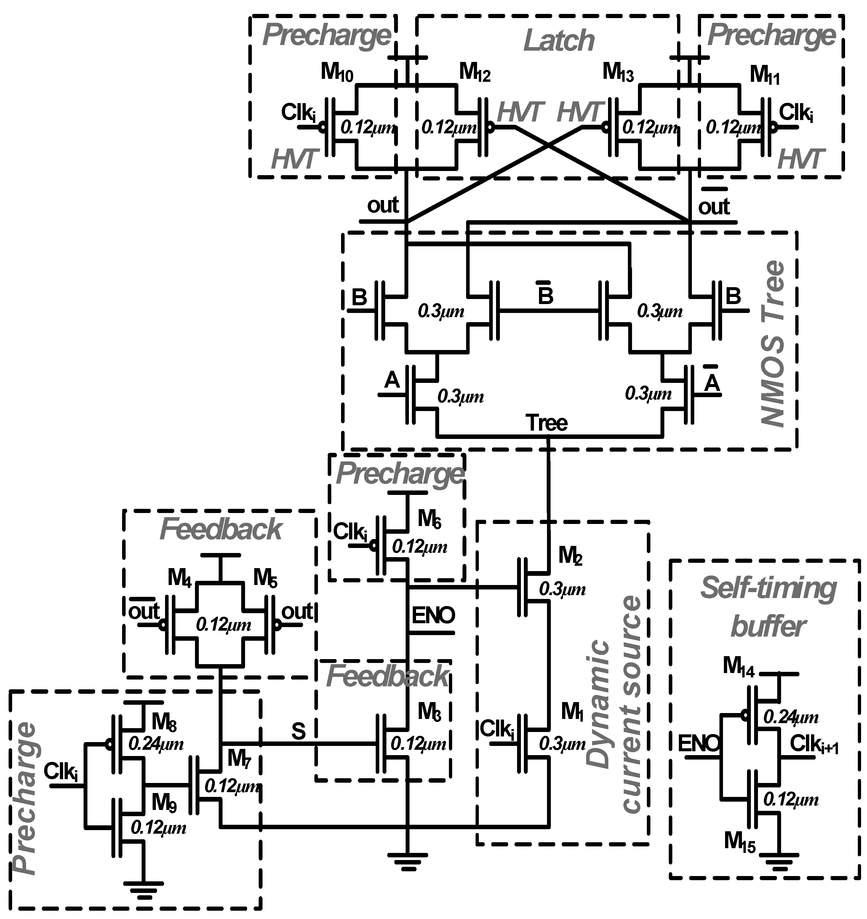
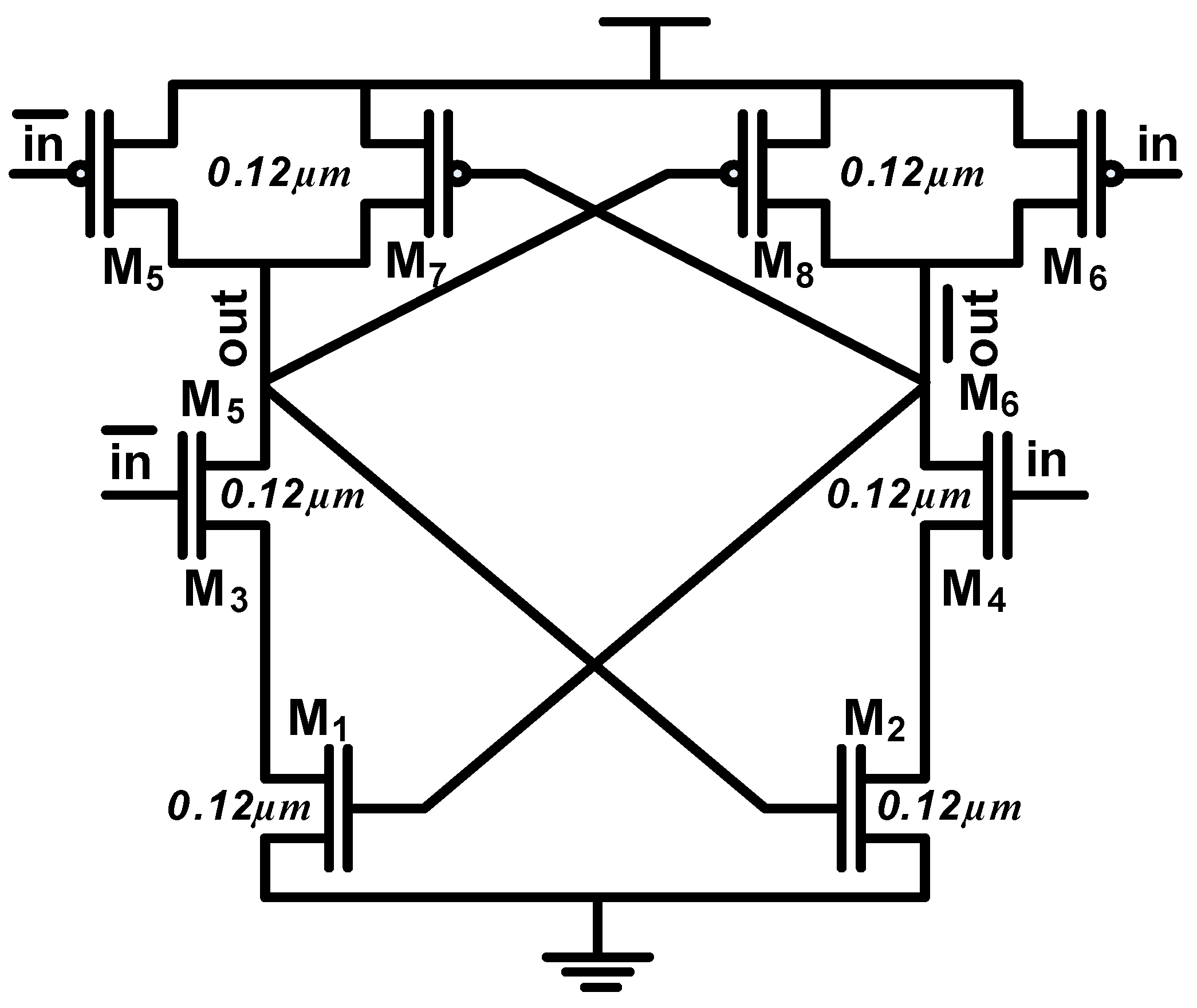
2.1. DDSLL Circuit Topology

Figure 1 shows the schematics of a simple XOR gate implemented using DDSLL. It uses the same NMOS tree as DyCML to evaluate the function at hand. Transistors M1 and M2 operate as the dynamic current source, while transistors M3–M5 perform the feed-back operation necessary for cutting off the current after evaluation. Transistors M6–M11 form the precharge circuit, and transistors M12 and M13 function as a latch. The self-timing buffer used for the DDSLL is a simple inverter as shown in Figure 1.

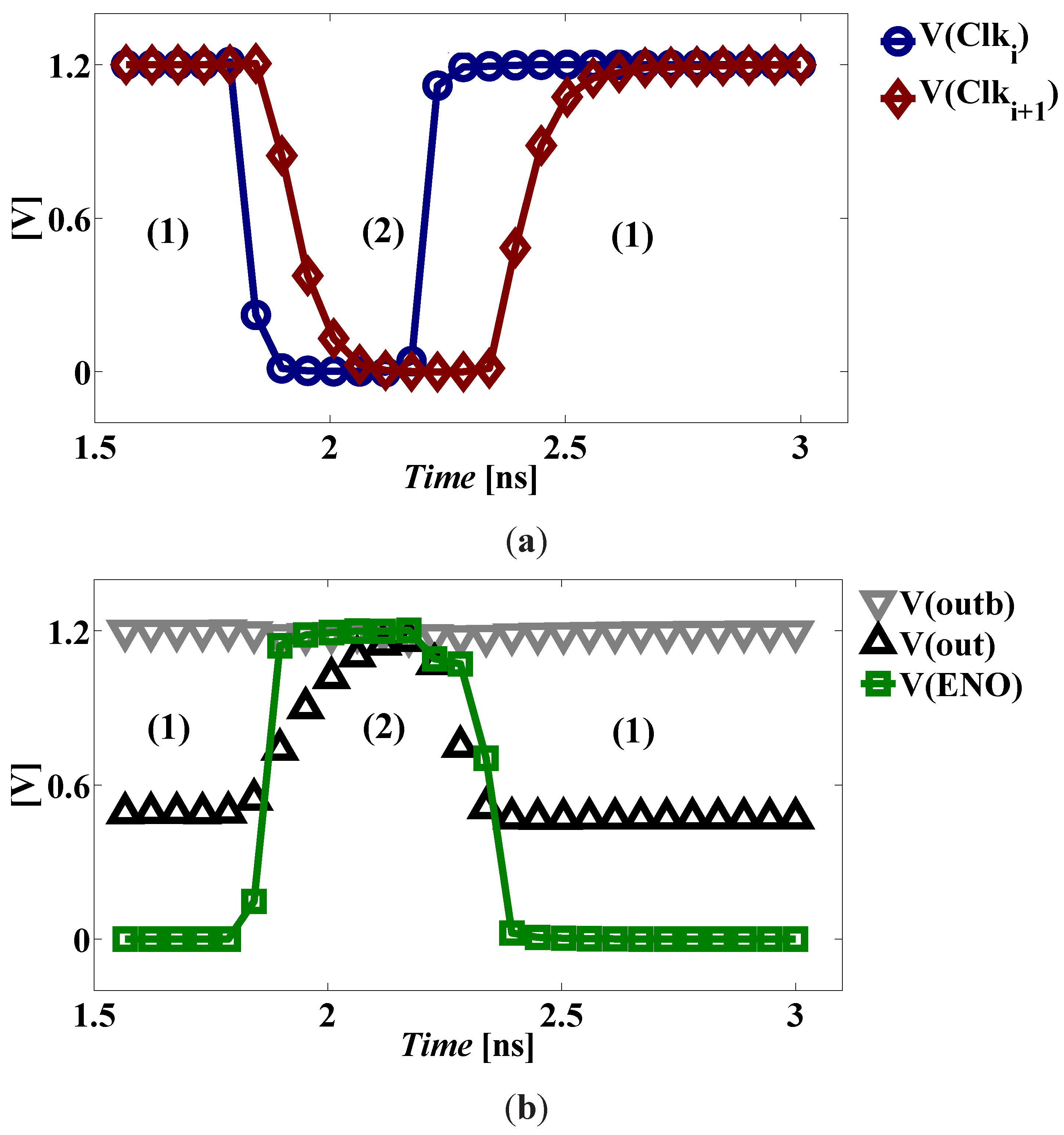
2.2. DDSLL Functional Operation

The operation of the DDSLL is quite simple. It consists of two phases: precharge and evaluation. Figure 2 shows how the precharge and evaluation phases function. During the precharge phase, the input clock signal Clki is low, discharging node S to GN D and charging node EN O to VDD. However, there is no current path from VDD to GN D as M1 is switched off. Meanwhile, both output nodes out and o u t ¯ are precharged to VDD via transistors M10 and M11.
During the evaluation phase, the input clock signal Clki is high, allowing current to flow through the dynamic current source (M1, M2), as node EN O was previously charged to VDD, in order to provide a discharge path for one of the precharged output nodes. Depending on the logic function and the inputs, there will be a single low impedance path from one of the output nodes to GN D. As soon as one of the output nodes falls below VDD − VtP |F B, where VtP |F B is the threshold voltage of the feed-back PMOS transistors, node S will be charged to VDD turning on the feedback transistor M3, which in turn discharges node EN O to GN D switching off the dynamic current source. Meanwhile, one of the latch transistors (M12, M13) turns on as the output node connected to its gate falls below VDD − VtP |L, where VtP |L is the threshold voltage of the latch PMOS transistors, preserving the voltage of the other output node at VDD. The self-timing buffer acts as the interface between cascaded stages of the DDSLL style, as it delivers a slightly shifted version of the input clock indicating the termination of the evaluation phase of the current block.

2.3. DDSLL Circuit Design

As was previously shown in [33], the choice of the technology node with the appropriate class (either general purpose (GP) or low-power (LP)) and device type greatly affects the circuit delay and power consumption performance. As a result, the LP 65 nm technology node is selected not only because of its economical impact, but also to reduce both the dynamic power and leakage power without sacrificing the performance.
With respect to the sizing of the transistors, all are designed with minimum gate length (Lg = 0.06 µm). As for the transistors width:
  • The precharge, latch, feed-back circuits and the self-timing buffer are designed using minimum feature size transistors (W = 0.12 µm) to reduce the power consumption except for the PMOS transistors in the inverters of the precharge circuit and self-timing buffer (W = 0.24 µm) to maintain the duty cycle of the input clock.
  • The dynamic current source uses wider transistors (W = 0.3 µm) in order to drive sufficient current from the NMOS tree during the evaluation period providing the desired output voltage swing.
  • The NMOS tree is also designed with wider transistors (W = 0.3 µm) for two reasons; the first is to increase the output voltage swing and the second to reduce the effect of WID variability on the output voltage swing.
Regarding the choice of the devices, this technology offers three different threshold-voltages (Vt) devices, low-Vt (LVT), standard-Vt (SVT) and high-Vt (HVT). Most DDSLL devices are chosen to be SVT devices to limit the leakage power without great loss of performance. Contrarily, the latch and transistors M10–M11 of the precharge circuit use HVT devices in order to reduce the leakage that charges the low-voltage output nodes during the evaluation phase especially at higher temperatures.

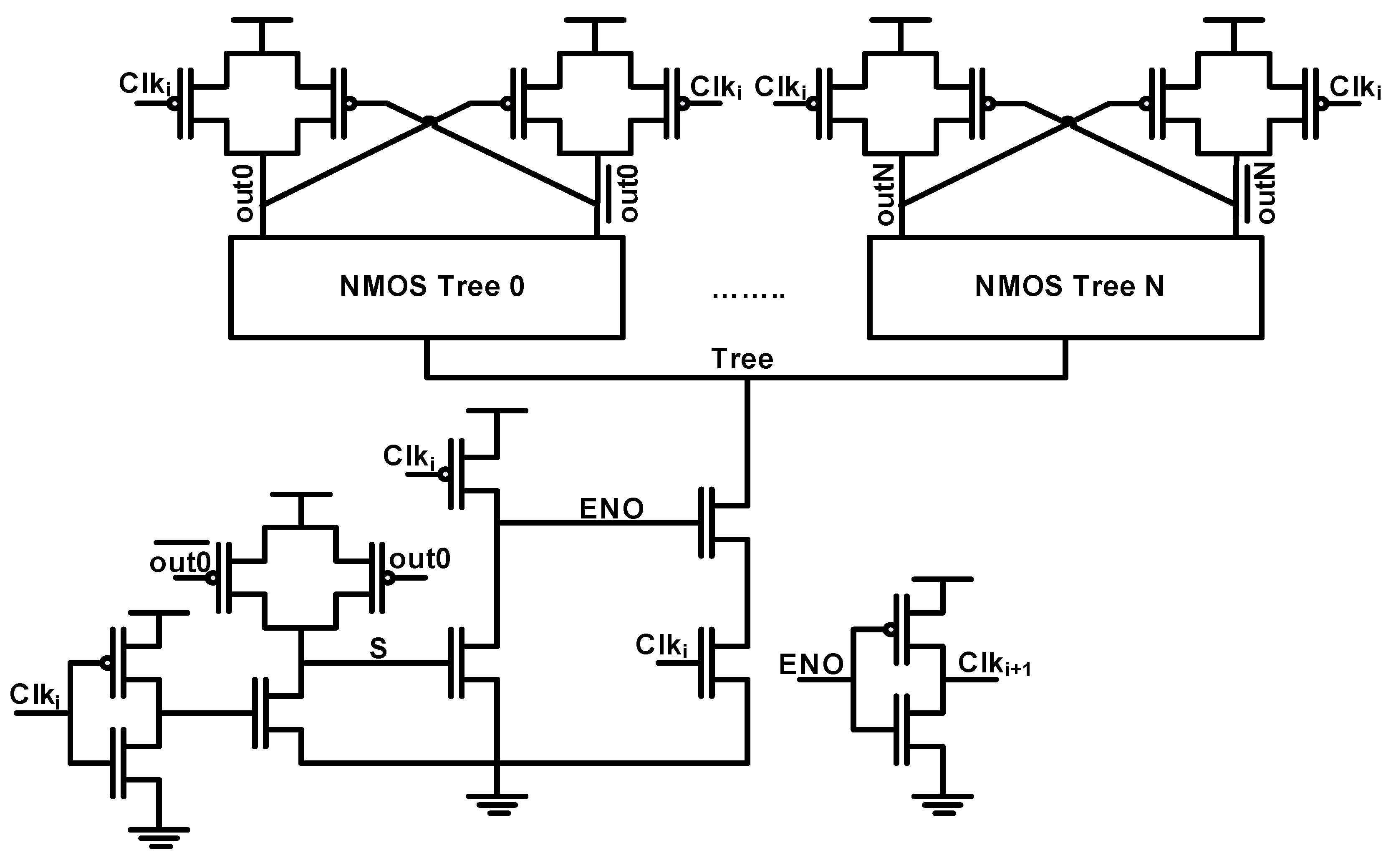
2.4. NMOS Trees Creation

Since the DDSLL style is developed as a countermeasure against power analysis attacks [19,34], special care has to be taken while designing the NMOS trees, especially since large NMOS trees can be used to implement complex functions with even three or four inputs in order to save area.
  • Both out and o u t ¯ of each NMOS tree must be connected to the same number of parallel branches in order to have the same load.
  • The number of series connected transistors in each out/ o u t ¯ branch should not depend on the input of the implemented function [35].
  • The layout of the NMOS tree should preserve the symmetry between out and o u t ¯ branches and also balance the routes in order to match the interconnect capacitances [35].
The NMOS tree representing a certain function can be easily created from the binary decision diagram (BDD) [36] used to define this function [37,38]. Accordingly, a tool based on BDD is proposed in [38] to explore different implementations of the targeted NMOS trees in order to predict the most secure structure.
From the layout point of view, [39,40] propose a technique that employs standard place and route tools to route the differential signals guaranteeing the matching of the interconnect capacitances within a few percent. However in the test chip of this paper, NMOS trees creation and layout are done in a full-custom manner. Although all three above mentioned items are equally important to guarantee input-independent power consumption, only items (1) and (3) are taken into consideration in this test chip. The main reason behind this design choice is to reduce both the power consumption and the area of the DDSLL gates. That is, if the number of series transistors in each branch of an NMOS tree is equalized, then the number of transistors per gate would increase leading to a higher power consumption and an enlarged area. As a result, we decided to implement the most compact NMOS tree considering items (1) and (3) only as a tradeoff between power consumption/area and security performance in this test chip.

2.5. Sharing Principle

The sharing of common blocks is generally used to reduce the power consumption overhead of these blocks and also to reduce the die size. It is applicable to differential current mode logic styles which are either dynamic such as DyCML or static as in MCML [41,42,43]. For example, in subthreshold MCML [41] the feedback bias circuit, which defines the gate voltage of the PMOS load devices, can be shared among several logic gates. Also in [43] the replica bias in the subthreshold source coupled logic (STSCL), which biases both the PMOS load devices and the tail current source, can be shared. However, sharing in these cases causes the design to be vulnerable to WID variability as the feedback bias/replica bias should be well matched to the MCML/SCL gates in order to minimize the deviation of the output voltage swing. As a result, a deviation of 40 mV in STCL for minimum size devices using 0.18 µm technology is reported by [43].
On the other hand, the principle of sharing in DDSLL is quite different. Figure 3 depicts the technique we introduce so that several NMOS trees can share the same feed-back, dynamic current source, self-timing buffer, and part of the precharge circuit. However, the latch transistors connected to the output nodes cannot be shared as they are needed for each output of the NMOS trees. Also the output precharge transistors are not shared, although they can be, because of the excess complexity that would be added at the layout phase. Accordingly, sharing is useful among gates whose operations can be performed at the same time, since in this case these functions will terminate their evaluation process at the same time. Therefore, they need a single dynamic source and a single self-timing buffer.
Finally, the out/ o u t ¯ of the NMOS tree that derive the shared feed-back circuit should be chosen to be the most loaded outputs. This way, the output clock Clki+1 of these shared functions is generated after the slowest output is evaluated which guarantees successful operation. In addition, this will increase the output voltage swing of the shared blocks as the slowest output will cut off the current of the dynamic current source after a longer period.

2.6. Interface with Static CMOS Logic

To interface the output of the DDSLL with the input of the static CMOS, a special buffer is needed to convert the DDSLL low-swing clocked signal to a full-swing non-clocked signal. Low-swing to full-swing buffers exist in literature, for example in [17]. However, it does not take into account the fact that the differential outputs are both precharged to VDD every clock cycle, while in static CMOS this is not the case. Therefore, the buffer interface needs not only to convert the low-swing signal to a full-swing signal, but also to preserve the evaluated output during the precharge phase of the clock.
Figure 4 shows the schematic of the proposed output buffer to interface the DDSLL with the static CMOS. All transistors are SVT devices with minimum feature size. The input signals in and i n ¯ are the differential low-swing outputs of the DDSLL style, while the out and o u t ¯ signals are the input signals to the static CMOS. In order to explain the functionality of the output buffer let us assume that during evaluation in is the low signal and i n ¯ is the high signal. During the evaluation phase, transistor M6 is on, charging node o u t ¯ to VDD, which in turn will switch on transistor M1. Now the two series NMOS transistors M1 and M3 are on discharging node out to GN D. During the precharge phase, both in and i n ¯ signals are high, turning on transistors M3 and M4. As a consequence, the output buffer acts as a latch preserving the voltages of the differential full-swing previously evaluated outputs. The operation of the output buffer is shown in Figure 5.
On another hand, the interface between the output of the static CMOS and the input of the DDSLL does not require special buffers, it is sufficient to directly connect the output of the static CMOS to the input of the DDSLL similar to [17].

3. Simulation Results of DDSLL and Other State-of-the-Art Logic Styles
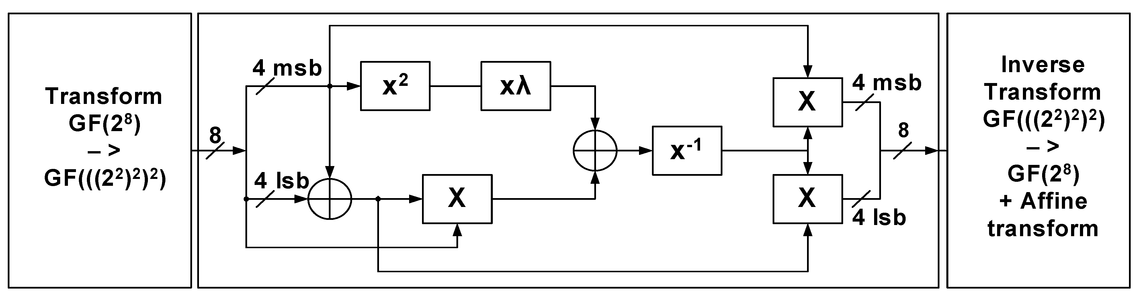
Simulations are done using SPICE at typical conditions (VDD = 1.2 V, temperature = 27 ◦C, typical NMOS and PMOS transistors). In this section we evaluate the power, delay and security performances of the DDSLL style and compare it to static CMOS and other DDL styles; namely DyCML and SABL. For this purpose, we chose the AES S-box [44] as the test case as discussed in the following section.

3.1. Case Study

In order to demonstrate the special features of the DDSLL style, a combinatorial circuit is designed using SABL, DyCML, DDSLL and static CMOS style as a reference. More specifically, an AES S-box [44] as implemented in [33], based on the proposed architecture of [45,46] is shown in Figure 6. It is an 8-bit input/output architecture, which is implemented using two versions of static CMOS; namely the 2-input static CMOS that limits the gates to simple 2-input XOR/XNOR, AND/NAND gates and the 4-input static CMOS that uses 4-input functions as needed besides the before mentioned 2-input functions. Also, SABL, DyCML and DDSLL S-boxes are implemented and the characteristics of all S-boxes are summarized in Table 1. The circuit implementation of all the DDL styles is quite simple, each function can be realized using a single NMOS tree and all functions that operate at the same time can be grouped to share the common blocks as discussed in Section 2. Pre-layout simulation results are available for both versions of static CMOS and all DDL styles, whereas post-layout simulation results are available for the 2-input static CMOS S-box and the DDSLL styles only. It is worth mentioning that the 2-input static CMOS S-box was initially designed with the intention to work at sub-threshold voltages.

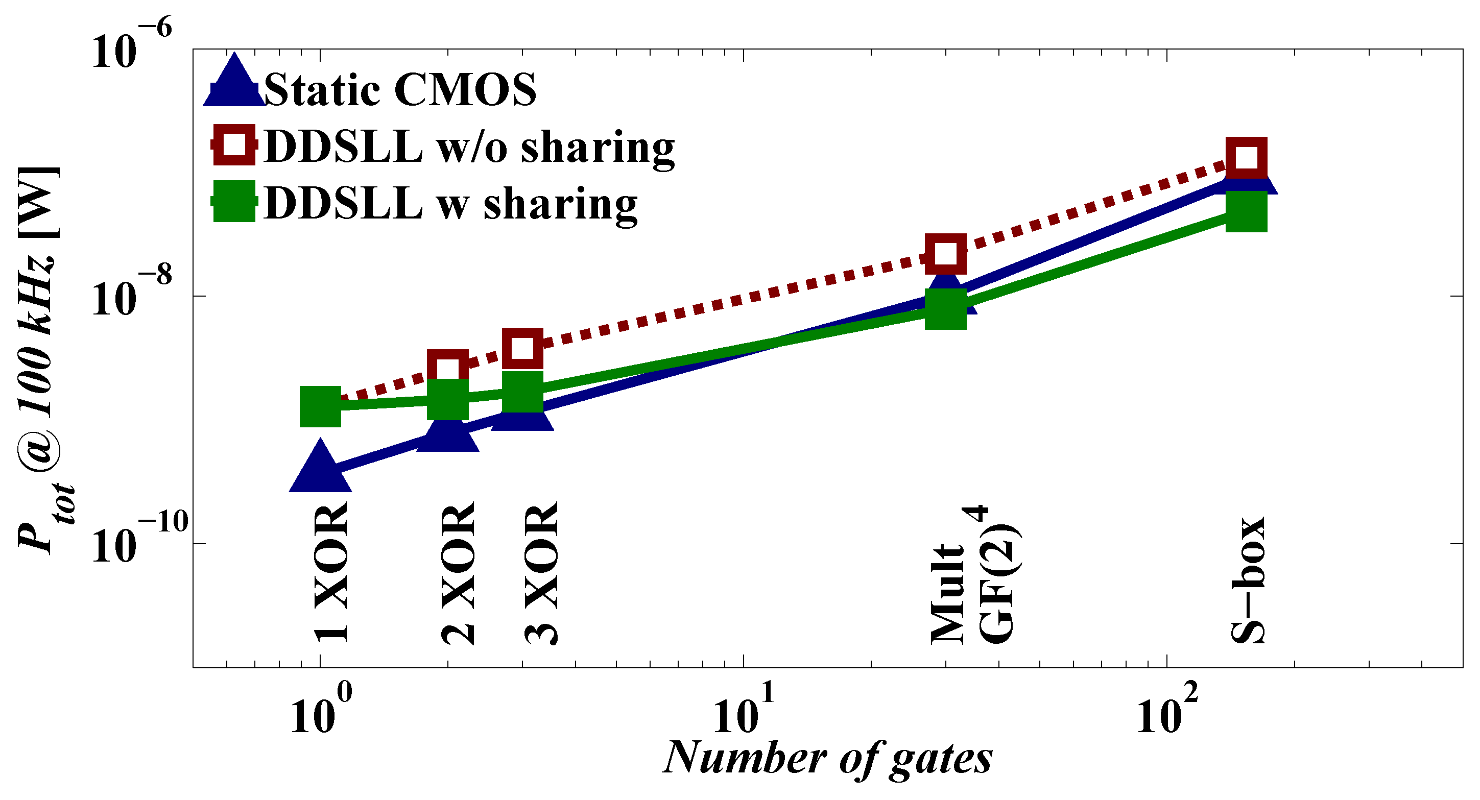
3.2. Effect of Sharing in Dynamic Differential Logic

Since the principle of sharing the common blocks is generally applicable to differential CML, this section will demonstrate its effect on the power consumption of the DDSLL style only. Figure 7 shows the total power consumption of several blocks implemented using 2-input static CMOS and DDSLL with or without sharing versus the number of gates used by the 2-input static CMOS blocks. Simulations are done at typical conditions (VDD = 1.2 V, temperature = 27 ◦C, typical NMOS and PMOS transistors) without adding the extracted routing parasitics (only gate capacitances are accounted for). It can be seen that the total power consumption of a single DDSLL XOR gate is almost 3× higher than that of a 2-input static CMOS XOR gate. Therefore, if DDSLL gates are implemented without sharing the common blocks, the power consumption is kept higher than that of the corresponding 2-input static CMOS blocks as seen for example in the case of the S-box. However, if the principle of sharing is applied to the DDSLL gates, then the power consumption tends to be lower than that of the 2-input static CMOS as the number of gates increases. As a result, the DDSLL S-box that uses the sharing principle consumes 2× less power than the 2-input static CMOS S-box and 2.7× less power than that without sharing. Knowing the fact that a 4-input static CMOS complex gate would have reduced dynamic and static power consumptions with respect to its 2-input static CMOS implementation, simulation results are conducted on the 4-input static CMOS S-box and its total power consumption is 24% less than the 2-input static CMOS implementation. If the power of the DDSLL S-box with sharing is compared to that of the 4-input static CMOS S-box, the reduction will be a factor of 1.5× (instead of 2× if compared to the 2-input static CMOS S-box). However, the power reduction brought by the principle of sharing in the DDSLL style is evident regardless of the static CMOS implementation.

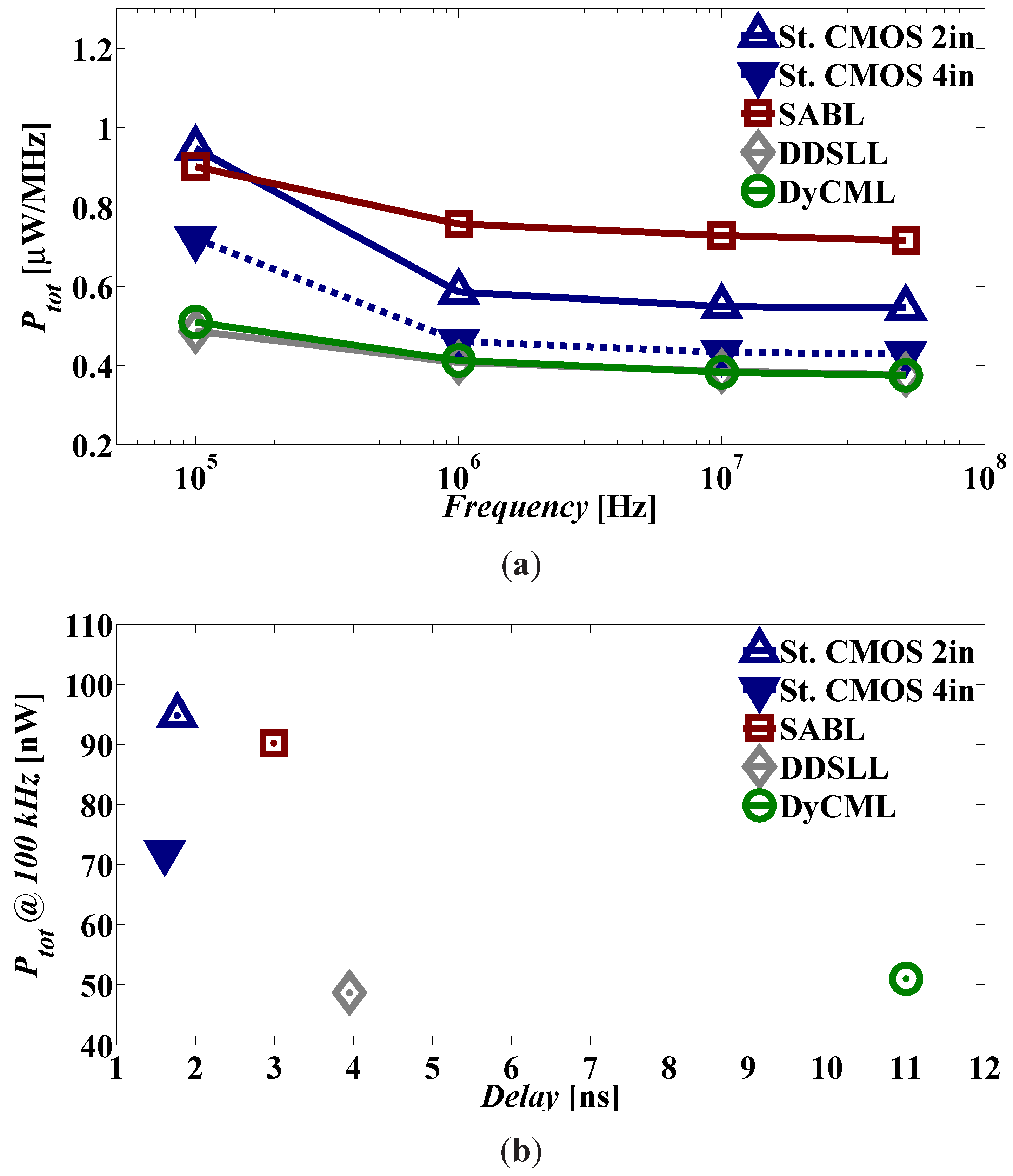
3.3. Power and Delay Comparison

As the simulation of the DDSLL S-box demonstrates a significant reduction of power thanks to sharing the common blocks, here we apply the sharing principle to the SABL, DyCML and DDSLL S-boxes and compare their power consumption to that of the 2-input and 4-input static CMOS S-boxes. The used test-bench simply consists of input and output buffers that have an independent supply source, whereas the S-box under test has a separate supply source that also acts as a meter to measure the current of the S-box under test. Simulations are done using ELDO SPICE simulator as in the previous section for 10 input transitions. It is worth reminding that both static CMOS and SABL are full-swing logics while DyCML and DDSLL are low-swing logics. In order to have a fair comparison between DDSLL and DyCML styles, the transistors of the latter are sized so that the output voltage swing is the same as that of the DDSLL. The power consumption is extracted by averaging over the 10 input transitions.
Figure 8(a) shows that the power consumption of SABL S-box is comparable to that of 2-input static CMOS at 100 kHz and starts to show a larger difference of about 30% above 1 MHz. However when compared to 4-in static CMOS S-box, the SABL S-box consumes even more power, 31% and 64% at 100 kHz and above 1 MHz, respectively. Figure 8(a) also shows that both the DyCML and the DDSLL S-boxes consume similar power which is almost 2× and 1.44× less than that of 2-input static CMOS S-box at 100 kHz and above 1 MHz, respectively. Nevertheless, when DyCML and DDSLL S-boxes are compared to 4-input static CMOS the power reduction is limited to 1.5× and 11% at 100 kHz and above 1 MHz, respectively. However, the power advantage of DDSLL and DyCML styles over SABL is clear; a reduction by a minimum factor of 1.8. Another interesting point is that above 1 MHz the static power starts to be negligible and the Ptot represented as µW/MHz is almost constant above 1 MHz. However at 100 kHz, where the static power has a significant contribution, the Ptot represented as µW/MHz is greater than that at higher frequencies. This is true for all logic styles, however for the DDL styles the contribution of static power at 100 kHz seems to be less than that of the two versions of static CMOS. Using rough calculations, the static power consumption is 40 nW, 28 nW, 16 nW, 11 nW and 9 nW for 2-input static CMOS, 4-input static CMOS, SABL, DyCML and DDSLL S-boxes, respectively.
The benefit of using a DDL style over static CMOS appears first in the reduction of the static power, more pronounced in DyCML and DDSLL due to the dynamic operation and in the use of a larger stack of transistors. However, not all DDL styles feature a reduced dynamic power. Although they all use the sharing principle discussed in Section 2.5 and they implement complex functions in single NMOS trees as explained in Section 2.4, SABL S-box consumes 64% more dynamic power than 4-input static CMOS S-box while DyCML and DDSLL S-boxes consume 11% less dynamic power than that of 4-input static CMOS. This is because DyCML and DDSLL are low-swing logics while SABL is a full-swing logic.
Concentrating on the power consumption of the AES S-box at 100 kHz versus the delay, Figure 8(b) shows that the DDSLL is the most suitable logic as it has a 2× and 1.5× reduction in power consumption compared to 2-input and 4-input static CMOS, respectively and only a 2× increase in delay. DyCML also shows the same power consumption as DDSLL, but has a greater delay penalty which is 6× higher than that of the two static CMOS versions. On the other hand, the SABL S-box consumes almost the same power as 2-input static CMOS with a 70% increase in delay.
Finally, it is worth mentioning that although the static CMOS S-box could be operated at a near- threshold supply voltage which would dramatically reduce its power consumption compared to DDSLL, we use the nominal 1.2 V supply for both S-boxes. Indeed, for cost concern, the target RFID tags and smart cards applications still favor operating at a nominal voltage to avoid multiple power domains on the chip, given that other circuitries such as the SRAM can hardly be operated at lower supply voltages. Another important aspect is security; it was shown in [24] that operating at a near-threshold supply voltage greatly affects the security performance of the static CMOS S-box due to the great impact of variability. As a result, the security evaluation of an implementation greatly depends on the choice of the supply voltage. In order to have a practical comparison from the application stand-point and a fair comparison of security, we thus maintain this choice of 1.2 V supply.

3.4. Security Simulation Results

In order to perform the security analysis, power traces of the 2-input static CMOS, SABL, DyCML and DDSLL S-boxes are extracted using SPICE simulations performed at a supply voltage of 1.2 V and at ambient temperature (27 ◦C) without adding any extracted routing parasitics (only gate capacitances are accounted for). In this section we implement template attacks [32] which are considered useful to estimate the worst-case scenario of information theoretic analysis. As a metric, the perceived information [30] is used. It captures how precisely the adversary’s leakage model can predict the actual information leakage distribution of the circuit at hand. Table 2 compares the perceived information of the 2-input static CMOS, SABL, DyCML and DDSLL S-boxes at the noise standard deviation extracted from the measurement traces (3.16 × 10⁻⁶). The DyCML S-box provides the minimum perceived information which is 2.7× less than that of 2-input static CMOS, followed by the DDSLL S-box which is 2× lower and finally SABL which is 1.5× only lower than 2-input static CMOS. The main reason behind these results is that the instantaneous power consumption and the standard deviation over the inputs are arranged in the same order. That is, the 2-input static CMOS comes first with the maximum instantaneous power consumption and the maximum standard deviation over the inputs, followed by SABL, DDSLL and finally DyCML. Interestingly, it was noticed in [31] that the time sample which maximizes the perceived information of the simulated traces corresponds to the one with the maximum standard deviation over the inputs, linking the perceived information to the standard deviation of the traces. Further details and analysis of the DDSLL S-box security performance compared to that of 2-input static CMOS are described in [31].

3.5. Effect of Routing Parasitics

The extraction of parasitic routing is done for the 2-input static CMOS and DDSLL S-boxes only at typical conditions and SPICE simulation results are obtained for 10 input transitions at 1.2 V supply voltage, 27 ◦C temperature and typical conditions of MOS transistors.
Table 3 demonstrates the effect of routing capacitance on both the power consumption and the delay of 2-input static CMOS and DDSLL S-boxes. Results of the power consumption are shown at 100 kHz (the minimum clock frequency for throughput/latency constraint in passive RFID tags [6]) and 13.56 MHz (the clock frequency of contactless smart cards - ISO/IEC 14443). It shows that the dynamic power consumption of the 2-input static CMOS S-box increases almost by a factor 2× due to routing. As for the DDSLL S-box, since it is a dynamic logic it is more practical to compute the total power which also increases by 2×. On the other hand, the delay of the static CMOS S-box increases by 1.4× while that of the DDSLL S-box increases by 1.8×. Subsequently, the impact of routing capacitance does not change our previous conclusions.

3.6. Variability Effect on the Power Consumption of DDSLL and Static CMOS Styles

In this section we concentrate on the variability of the dynamic power consumption. This is motivated by two facts. Firstly, even at 100 kHz, which is the lower bound of the frequency range of RFID tags, the dynamic power consumption of the 2-input static CMOS S-box is dominating (70%) as seen from Table 3. Moreover, the dynamic power of the DDSLL style is inherently dominating. Throughout, only the 2-input static CMOS will be considered, therefore it will be named static CMOS for simplicity.
The dynamic power consumption comprises two components, a switching component (PSW ) and a short-circuit component (PSC ). Knowing that the short-circuit power is usually 10% of the total dynamic power Pdyn at nominal VDD [47], the following analysis will only consider the switching component of the dynamic power. Accordingly, the Pdyn expression of an n-gate circuit is:
P d y n = g a t e P S W = V D D 2 × f c l k × j = 1 n ( α F , j . C L , j )
where VDD is the supply voltage, fclk is the clock frequency, αF,j represents the activity factor and CL,j the load capacitance of the jth gate.
Monte-Carlo SPICE simulations are conducted at 1.2 V supply voltage, 27 ◦C temperature at 100 kHz clock frequency. The dynamic power of the DDSLL S-box is calculated by averaging over the extracted transient part of the current and multiplying it by VDD. Simulation results show that the Pdyn histograms of both WID and D2D variabilities can be modeled as normal distributions. Therefore, Pdyn can be viewed as a summation of normally distributed random variables (αF .CL) as VDD and f are constants.

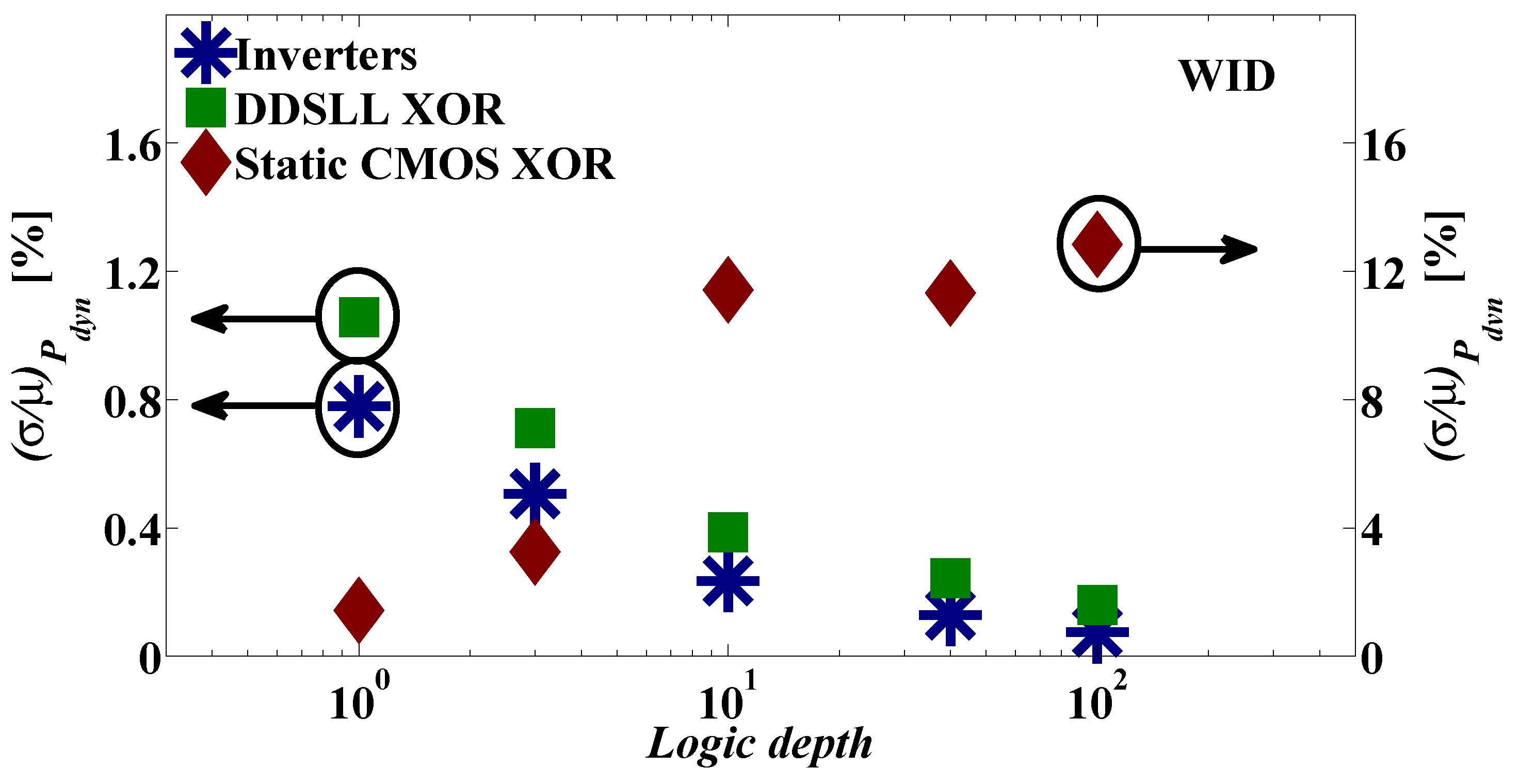
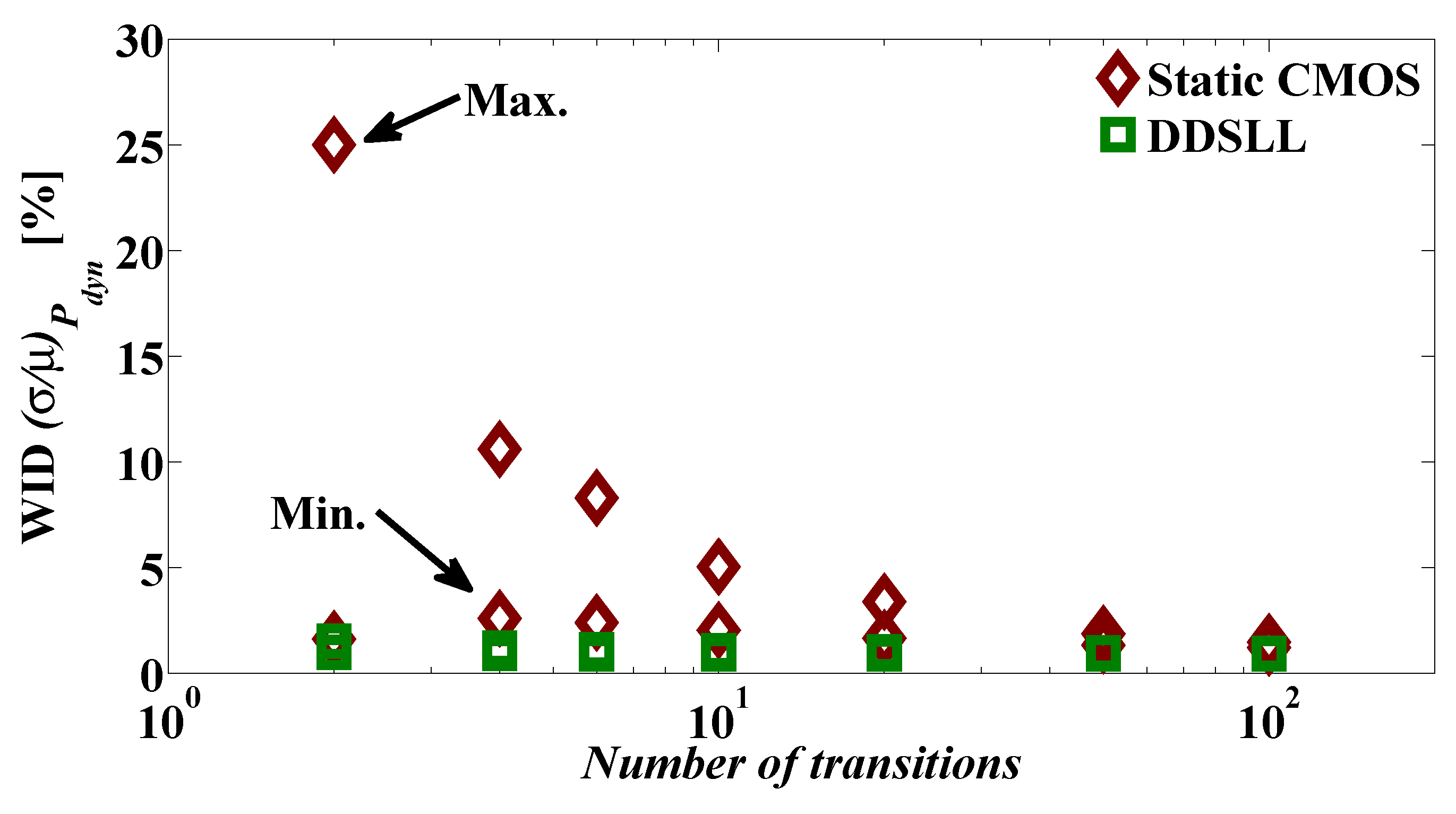
3.6.1. With-in-Die Variability

With respect to the WID (local) variability, it is a well known fact that the WID CL variability is quite small [48,49]. Indeed, CL is the sum of the gate output capacitance, the input capacitance of the subsequent gate and the routing capacitance. The authors in [48] mention that the routing capacitance variation is the dominant contributor, whereas in [49] only the input gate capacitance variation due to random dopant fluctuations is considered. In this paper the routing capacitance variation is not considered as it is not provided in the models used in simulations. Therefore, only the gate input capacitance is considered. As shown in [49], for a device with 30 nm channel length and 30 nm width, the normalized standard deviation (σ/µ) of CL (input gate capacitance contribution) is below 1% at 1 V. This is also validated in Figure 9 by performing Monte-Carlo SPICE simulations of a single inverter which results in (σ/µ) of Pdyn below 1% at 1.2 V. Clearly in the case of the inverter, the only source of variability is the WID CL since αF is fixed. Moreover, as WID CL variations are uncorrelated, they are averaged out as the number of gates n in an inverter chain increases:
Jlpea 02 00098 i001
which is also confirmed by the logic depth dependence of the inverter as depicted by Monte-Carlo SPICE simulations in Figure 9.
Now, in order to take the effect of αF on the WID variability into account, a static CMOS XOR chain with different logic depths is studied. Here, the two inputs of any XOR gate in the chain are driven by the output of the previous gate and the same input as the first XOR gate in the chain to magnify the WID αF variability. First, the sources of αF are identified as topology, signal statistics and spurious transitions or glitches associated to delay skew and logic depth [47]. Consequently as the logic depth increases, the delay skew between the two inputs of an XOR gate in the chain increases, generating random glitches, hence αF variations. As a result, the WID variability of the (αF .CL) term in Equation (1) is no longer decreasing with the increase of logic depth, but it actually increases as shown in Figure 9. Contrarily, the Pdyn WID variability of the DDSLL XOR chain decreases as the logic depth increases as shown in Figure 9 in accordance with the case of the inverter chain, thanks to having a deterministic αF , as it is glitch-free thanks to the self-time operation.

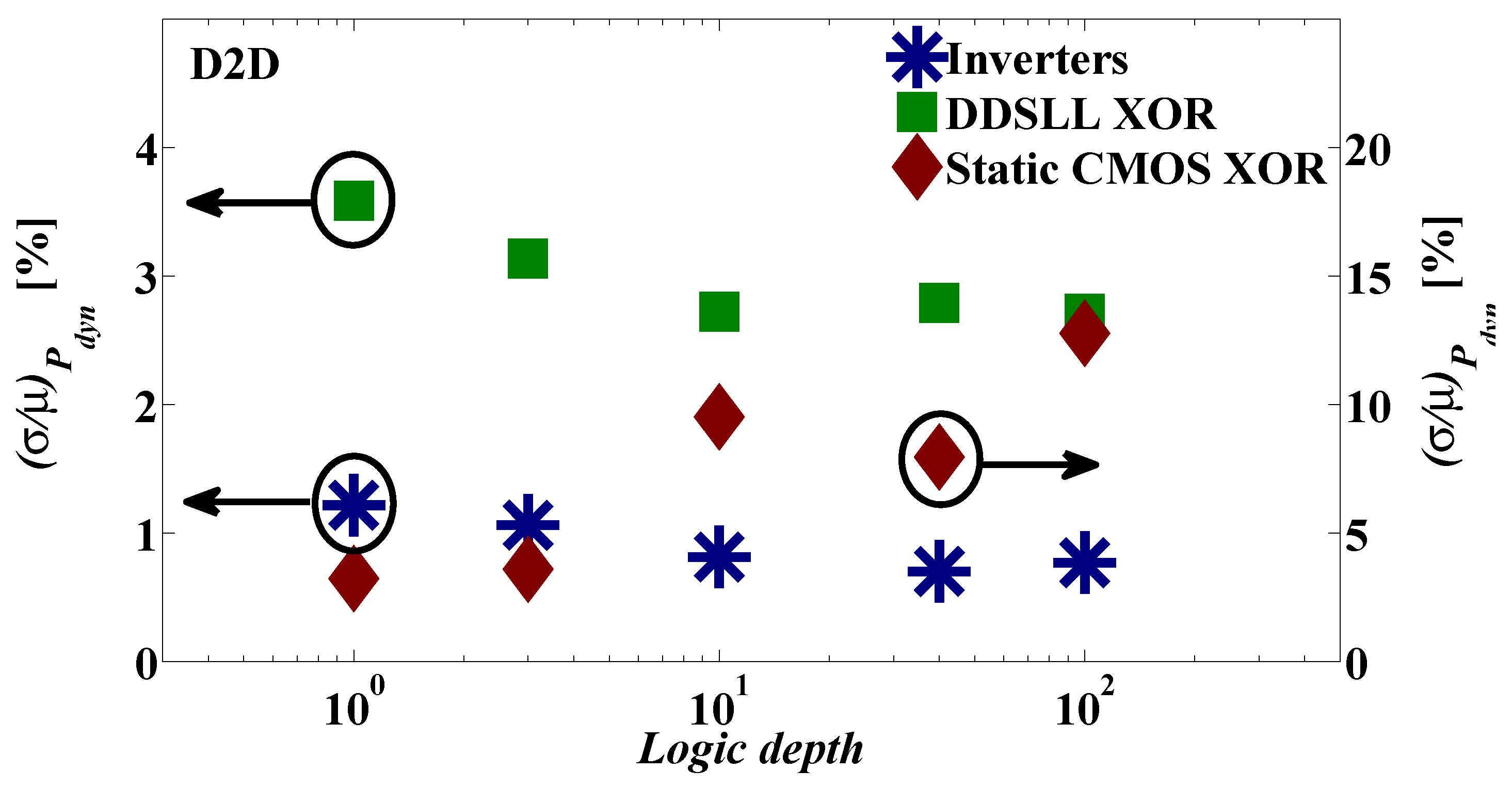
3.6.2. Die-to-Die Variability

The D2D (global) variability is spatially-correlated and it impacts all transistors in the same way. Therefore, in the cases where αF is deterministic, the D2D CL variability is independent of the number of stages as seen by the Pdyn normalized standard deviation (σ/µ) of the inverter and the DDSLL XOR chains in Figure 10. As for the static CMOS XOR chain, again the Pdyn normalized standard deviation (σ/µ) is dependent on the D2D variability of αF such that it increases with the increase of logic depth as shown in Figure 10.

3.6.3. WID Variability Effect on S-Box

In order to further demonstrate the importance of taking into account the effect of αF on the WID variability of Pdyn, Figure 11 compares the normalized standard deviation (σ/µ) of Pdyn of both static CMOS and DDSLL S-boxes, where Pdyn is averaged over different numbers of input transitions at 100 kHz. Clearly in the case of the static CMOS S-box, (σ/µ) of Pdyn varies between 1.6% and 25% for a 2-transition input pattern as a direct result of variations in αF . However, the increase in the number of transitions in the input pattern leads to a reduced WID variability around 1.3% which further manifests the effect of averaging over the number of input transitions. On the other hand, the DDSLL S-box shows almost a constant (σ/µ) of Pdyn around 1% only thanks to its deterministic αF .
The same conclusion is drawn in [28] by analyzing the Edyn total variability of the static CMOS S-box at low voltages where it is dominated by the WID αF variability. It is worth mentioning that the D2D αF variability is far less important in this case as measurements are done on the same wafer.
As a result, for low-power constrained applications such as RFID and smart cards, the impact of variability on the dynamic power plays an important role. In the case of high yield, the typical Pdyn+3σ should be less than the allocated power budget (dynamic). For a worst case scenario, a 2-transition input pattern is considered. For static CMOS, if the typical Pdyn at 100 kHz is 108 nW (as shown in Table 3) and the worst case σ is 27 nW (derived from Figure 11), then the typical Pdyn + 3σ would be 189 nW. While for DDSLL, if the typical Ptot at 100 kHz is 96 nW (also shown in Table 3) and the worst case σ is 0.96 nW (also acquired from Figure 11), then the typical Pdyn + 3σ would be 95.9 nW. Clearly the advantage of DDSLL is seen where the process variability has limited effect on its power consumption (keeping its power consumption within the allocated budget) whereas this is not true for static CMOS since process variations can cause the typical Pdyn + 3σ to be almost 1.75× the typical Pdyn.

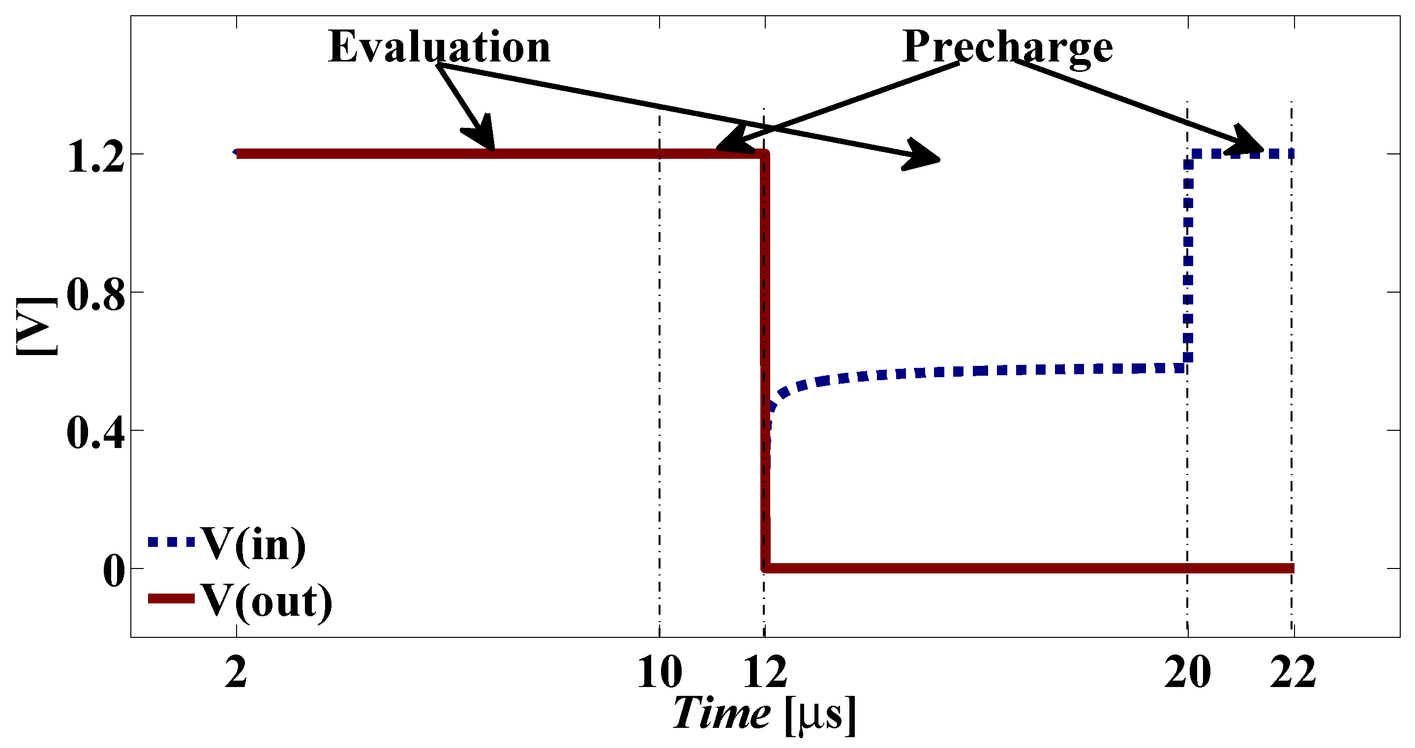
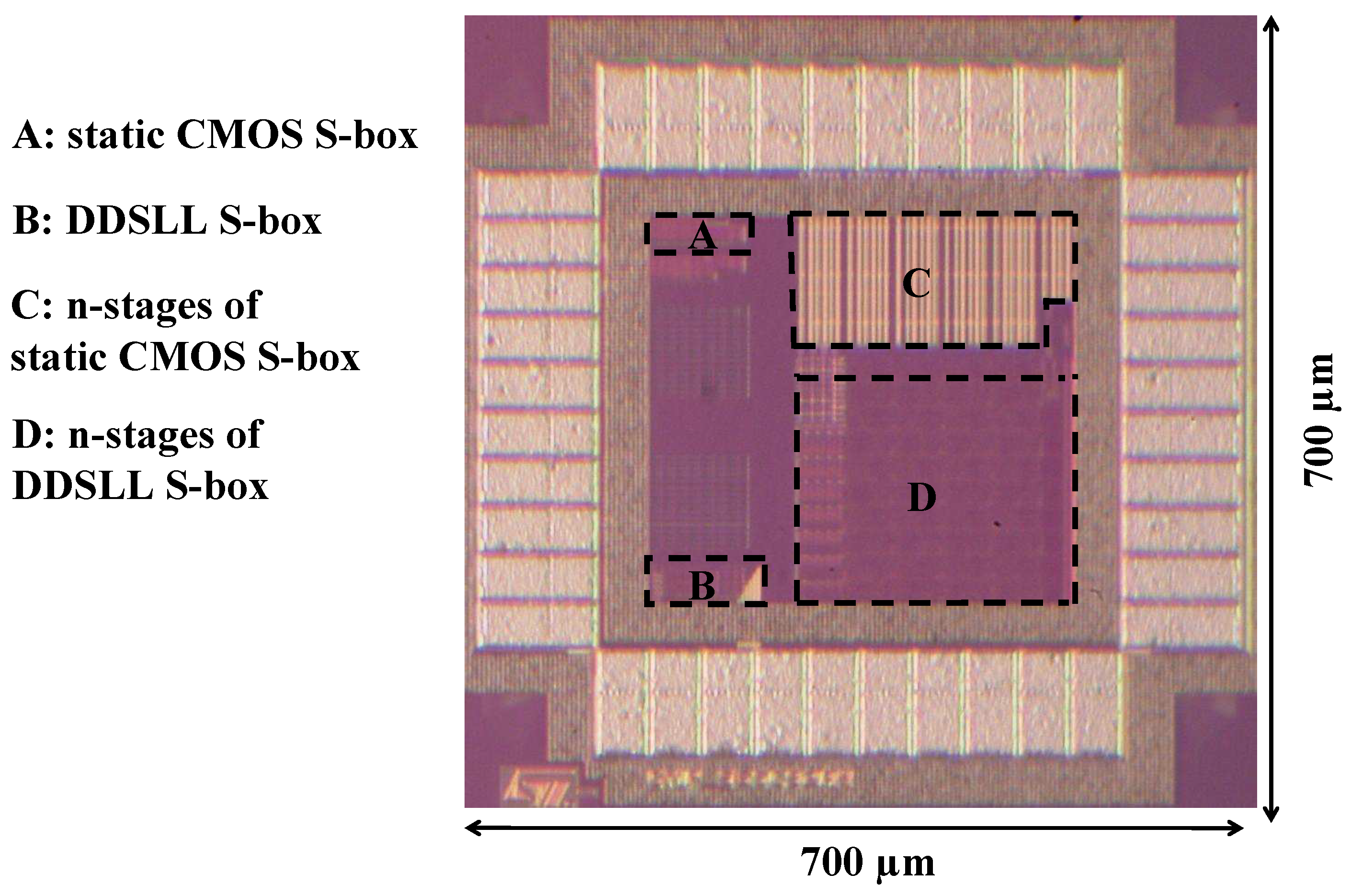
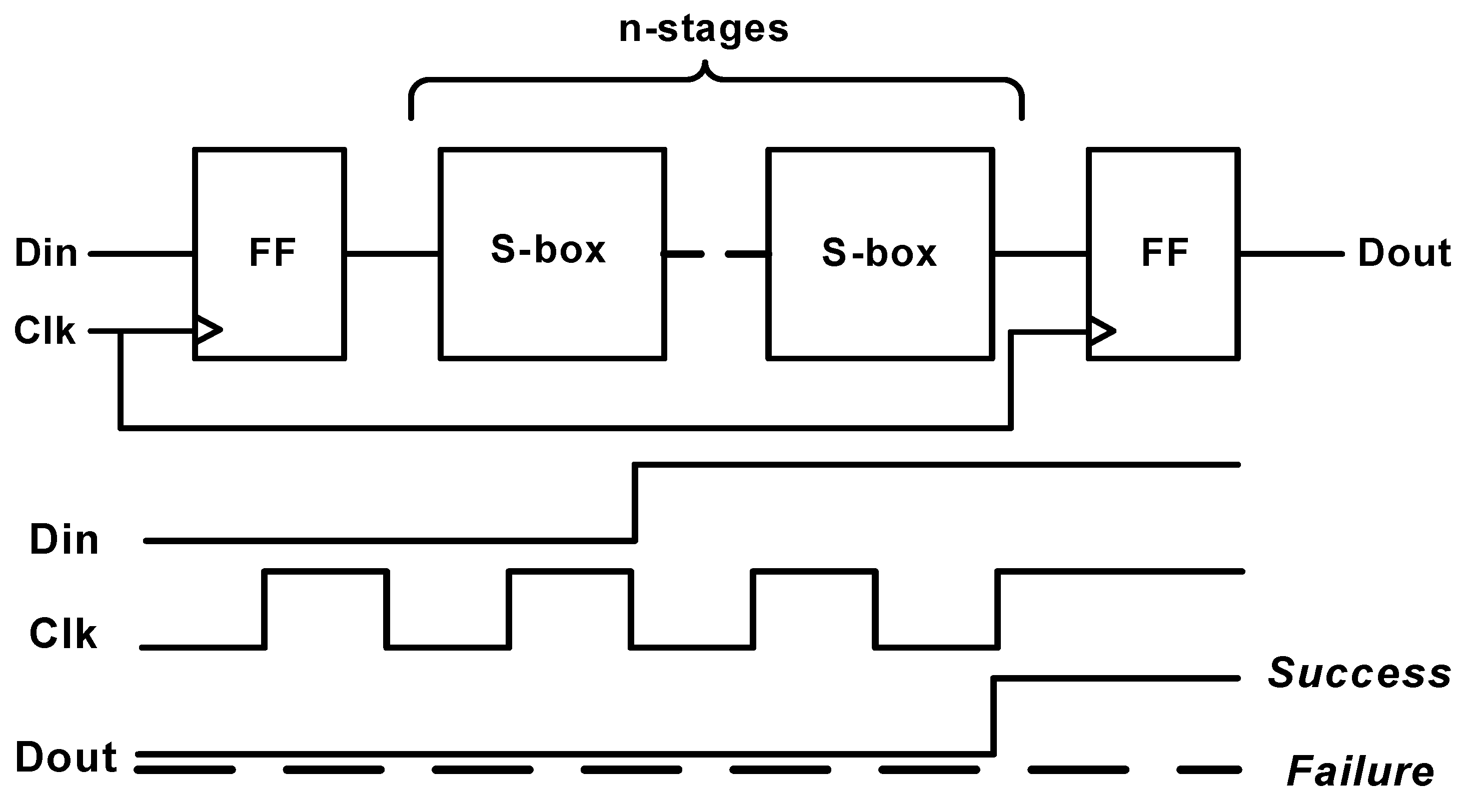
4. Measurement Results

Measurements are performed using the same conditions as in simulations. That is, at 1.2 V supply and at ambient temperature. The test chip is described in the following section, where only the static CMOS and DDSLL S-boxes are implemented. Measurement results are based on data from 20 dies.

4.1. Test Chip Implementation

A test chip was fabricated in order to confirm the power, delay and security performances of the DDSLL S-box and comparisons to a reference static CMOS S-box are made. Here the static CMOS implementation uses SVT devices only with minimum gate length and 0.12/0.24 µm wide NMOS/PMOS transistors. For the static CMOS S-box, the same device type; namely the SVT device, is chosen in order to have a fair comparison with the DDSLL S-box with the same parameters that are independent on the the exact technology. On the other hand, the DDSLL S-box is designed as explained in Section 2 with a target of minimizing both the area and the power consumption. As a result, the area of the DDSLL
S-box is 1125 µm2 which is only 12% larger than its counterpart in static CMOS. It is worth mentioning that the static CMOS implementation is done using 2-input gates only as the target was to test the static CMOS S-box at sub-threshold voltages. However, for the sake of a fair comparison, implementing the 4-input static CMOS S-box would have been more appropriate. Nevertheless, the comparison still stands with respect to the simulation results as it gives us an idea of how the measurements comply with the simulations.
Figure 12 shows the microphotograph of the test chip which has been fabricated using a 65 nm low-power (LP) CMOS technology. The test chip comprises two blocks consisting of stand-alone S-boxes for power consumption measurements in static CMOS (block A) and DDSLL (block B) logics. Also to measure the delay performance of both logic styles, two blocks consisting of 34 stages and 40 stages of chained S-boxes in static CMOS (block C) and DDSLL (block D) styles, respectively are realized.

4.2. Measurement Setup

The measurement setup consists of a 100 MHz digital waveform generator/analyzer (NI 6552) to provide the 8-bit input pattern to the S-boxes and the clock signal to the DDSLL S-box. It also consists of three power supplies for ESD, I/O buffers and for sourcing the voltage to the power supply of the S-box under test and measuring the current drawn from it. A Keithley 236 SMU is used here as its current sensitivity is 10 f A. In addition, for security assessment through current trace measurements, a resistor of 1 kΩ is inserted in the path of the VDD rail of the S-box under test to monitor the power consumption.

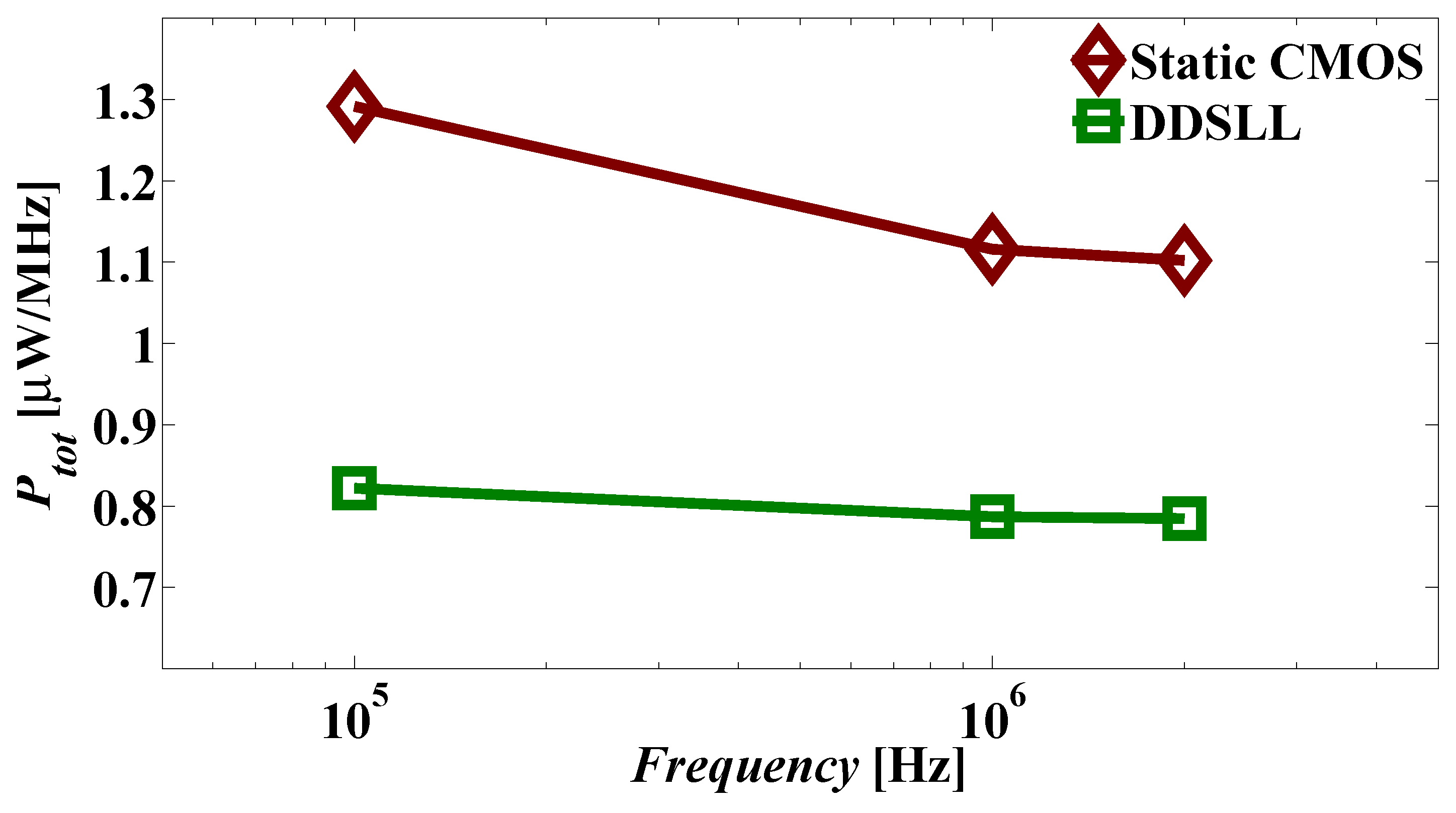
4.3. Power Consumption Measurement Results

The power consumption of both static CMOS and DDSLL S-boxes is measured using an input pattern consisting of 10 transitions (same as the one used for simulations) at 1.2 V and room temperature. In the case of static CMOS S-box, the static power consumption Pstat is measured by introducing constant inputs, then averaging over the corresponding leakage currents and multiplying by the supply voltage. The dynamic power is the result of subtracting the static power from the total power. In the case of DDSLL S-box, only the total power consumption can be measured. For both S-boxes, the measured power consumption results are averaged over 20 dies.
The comparison between measured and simulated power consumption of both static CMOS and DDSLL S-boxes is given in Table 4. Looking at the static power consumption of the static CMOS S-box, one can fairly assume that the measured dies are between an SS corner (slow NMOS, slow PMOS) and the TT conditions (typical NMOS, typical PMOS). This is because at TT conditions the simulated static power is 46.6 nW, while at SS corner it is 9 nW. On the other hand, the measured dynamic power of the static CMOS S-box is accurately predicted by simulations as both TT conditions and SS corner render the same dynamic power. Accordingly, the measured total power of the static CMOS S-box is 18% less than simulation at TT conditions. It is worth mentioning that according to the measurement results of the static CMOS S-box, the static power is 16% of the total power at 100 kHz. As for the DDSLL S-box, the measured total power is 14.4% less than the total power predicted by simulation at TT conditions.
Finally, Figure 13 shows the same trend as simulations for the total power consumption versus frequency for both static CMOS and DDSLL S-boxes (Figure 8 in Section 3.3). As explained before, the static power can almost be neglected above 1 MHz, whereas at 100 kHz it has a substantial share for both static CMOS and DDSLL S-boxes. However for DDSLL, the contribution of static power at 100 kHz seems to be less than that of static CMOS, confirming the results obtained from simulations. Using the same calculations as for simulation, the static power consumption is 19.5 nW and 3.9 nW for static CMOS and DDSLL S-boxes, respectively, which for the case of static CMOS matches the measured static power calculated for constant inputs in Table 4. To conclude, the measured power reduction brought by the DDSLL S-box is found to be 35% which is fairly predicted by simulation (37.8%) compared to 2-input static CMOS S-box.

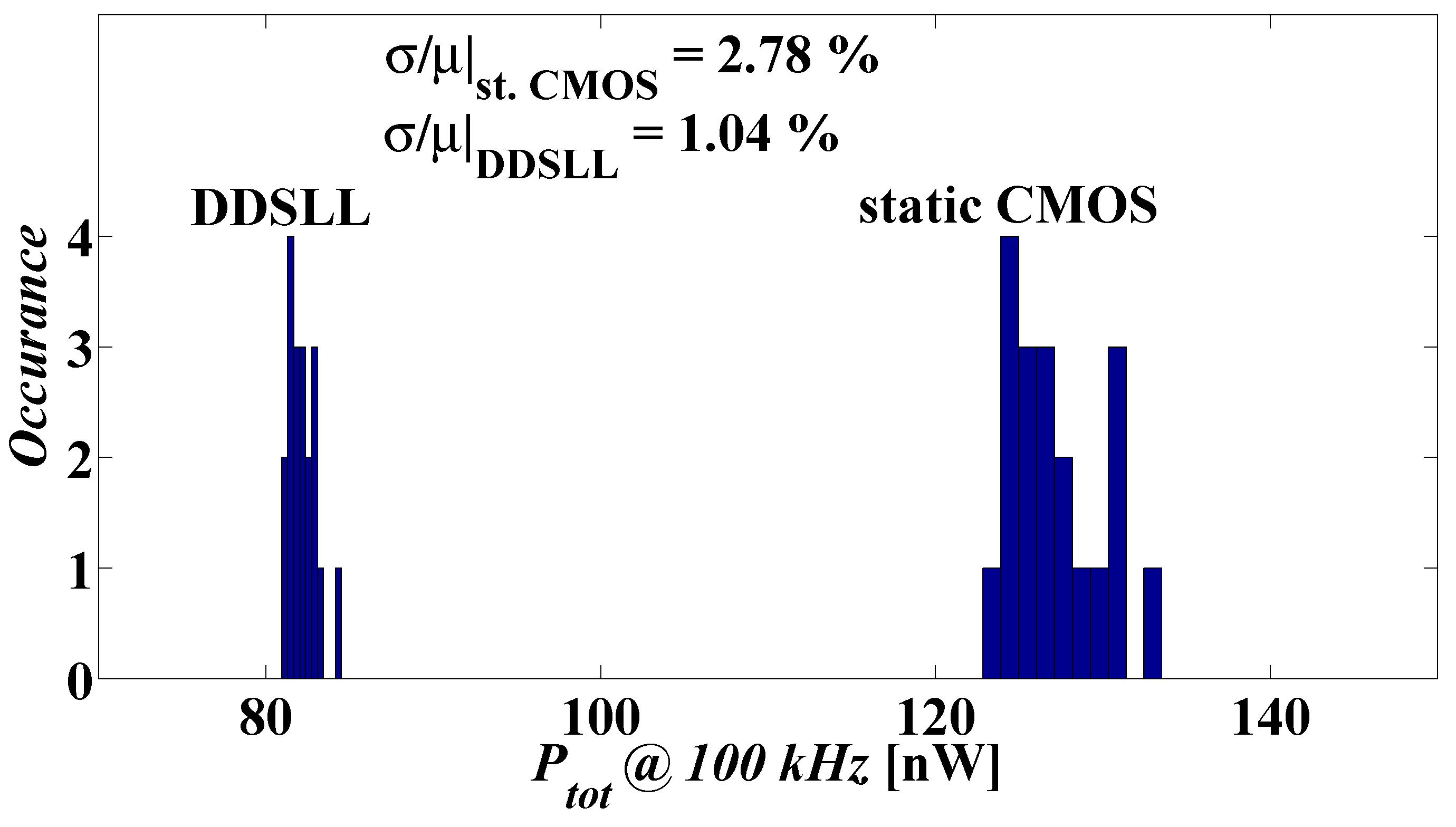
4.4. Variability Effect on Power Consumption Measurement Results

Measurements are done on 20 dies at 100 kHz, ambient temperature with 1.2 V supply for 10 input transitions in order to assess the variability of the power consumption of both the DDSLL and static CMOS S-boxes. Figure 14 shows the histogram of the total power consumption of both S-boxes at 100 kHz. The total variability (σ/µ) of DDSLL S-box is 1.04% and that of static CMOS is 2.74%. This complies with the simulation results as the DDSLL S-box shows dynamic power WID variability of about 1% for all input patterns, while the static CMOS S-box shows dynamic power WID variability ranging from 2% to 5% for a set of 10 input transitions.
As a result, the worst case maximum power, considering 6σ for high yield, is 147.6 nW for static CMOS and 87.3 nW for DDSLL resulting in a worst case power ratio of 1.69× instead of the 1.54× ratio in the case of typical power consumption. The difference between the worst case and typical ratios is not very high because in the measurements we considered 10-transition inputs, whereas if 2-transition inputs were considered as a worst case scenario, the difference between the worst case and typical ratios would have been more significant as demonstrated with Monte-Carlo simulations in Section 3.6.3.

4.5. Delay Measurement Results

The delay of both S-boxes is measured over a chain of n-stages between two flipflops as this relaxes the requirements of the test equipment. Figure 15 shows the block diagram and the waveforms of the test bench used to measure the delay of either S-box. Here, two flipflops are clocked by the same Clk signal, where the one at the beginning of the chain is used to toggle a single transition in Din signal through the n-stages of the S-box chain and the other one at the end of the chain is used to capture the transition of the output of the last S-box in the chain Dout. By reducing the clock period to the same range of the chain delay, the output flipflop will not be able to sample the transition of the output of the last S-box in the chain due to setup time violation indicating that this clock period represents the delay of the chain. For the static CMOS S-box, the chain is constructed of 34 stages, whereas the DDSLL S-box chain consists of 40 stages.
Table 5 compares the delay measurement results to the simulation results of both the static CMOS and DDSLL S-boxes. It is clear that the measured delay of both S-boxes is higher than that predicted by simulation at TT corner, which further proves the assumption made in Section 4.3 that the measured dies are closer to an SS corner than to a typical one. However, the increase in the measured delay of the static CMOS S-box compared to simulation is 24% while that of the DDSLL S-box is 8.3% only, confirming again the lesser sensitivity of the DDSLL style.

4.6. Security Results

As in Section 3.4, the current traces of the measured static CMOS and DDSLL S-boxes are first extracted and then the perceived information metric [30] is calculated while considering template attacks [32]. Table 6 compares the perceived information of the static CMOS and the DDSLL S-boxes at the measurement noise standard deviation (3.16 × 10⁻⁶). The DDSLL S-box has a perceived information that is 3× less than static CMOS which confirms the results obtained from simulations in Section 3.4. A detailed information theoretic analysis is discussed in [31]. It concluded that when template attacks (worst-case scenario) are conducted on actual measurement current traces and using the “measurements to disclosure” (MTD) metric, the DDSLL S-box demonstrates about an order of magnitude security improvement over its static CMOS counterpart.

5. Conclusions

Although static CMOS features low-power operation and small chip area, it fails to comply with the basic requirement of secure applications which is to hide the secure information. Therefore DDL styles were proposed to mitigate this deficiency, among which the DDSLL style. Taking into consideration the two main challenges of low-power secure applications, namely the power consumption and the chip area, DDSLL presents an interesting option as its measured power consumption is 35% less than static CMOS (implemented using 2-input gates). On the other hand, simulation results show that SABL consumes the same power compared to 2-input static CMOS and 31% more power compared to 4-input static CMOS at 100 kHz. It is clearly seen that DDSLL is more power efficient than SABL. Furthermore, the chip area of the DDSLL S-box is only 12% larger than static CMOS. However, the main drawback of DDSLL is the delay penalty which is 2.5×, but for relaxed timing constraint applications such as RFIDs and smart cards this is not an issue. In this work we also emphasize the importance of sharing the common blocks as it reduces the power consumption of the S-box 63%.
Although process variability is considered to improve the security performance of static CMOS against PA attacks, it is studied here from another perspective. The variability of the dynamic power consumption of the DDSLL style (which is also applicable to similar DDL styles) is addressed for the first time to the authors’ knowledge. The dynamic power consumption of DDSLL features constant WID and D2D variabilities thanks to its glitch-free operation, whereas static CMOS shows a great dependency on the activity factor as the logic depth increases. As a result, the worst case dynamic power ratio between static CMOS S-box and DDSLL S-box would be 2.65× as demonstrated by Monte-Carlo simulation results (considering here the total power of DDSLL instead of its dynamic power since its static power is proved to be negligible).
As for the security assessment, using the perceived information metric, measured results of DDSLL demonstrate a 3× security improvement over its static CMOS counterpart. Nevertheless from simulations, the DyCML style proves to be the most secure logic as it has a security margin of 2.7× with respect to static CMOS, compared to 2× and 1.5× for DDSLL and SABL styles, respectively. Yet, DDSLL provides a better low-power area-efficient solution compared to other DDL styles with significantly enhanced security performance compared to static CMOS.

Acknowledgments

Bol and Franc¸ois-Xavier Standaert are postdoctoral and associate researchers of the Belgian Fund for Scientific Research (FNRS - F.R.S.), respectively. This work was supported in part by the Walloon Region project E-USER (WIST program).

References

  1. Roberti, M. A 5-cent breakthrough. Available online: http://www.rfidjournal.com (accessed on 16 March 2012).
  2. Umeda, T.; Yoshida, H.; Sekine, S.; Fujita, Y.; Suzuki, T.; Otaka, S. A 950-MHz rectifier circuit for sensor network tags with 10-m distance. IEEE J. Solid State Circuits 2006, 41, 35–41. [Google Scholar] [CrossRef]
  3. Hong, Y.; Chan, C.F.; Guo, J.; Ng, Y.S.; Shi, W.; Leung, L.K.; Leung, K.N.; Choy, C.S.; Pun, K.P. Design of Passive UHF RFID Tag in 130 nm CMOS Technology. In Proceedings of the IEEE Asia Pacific Conference on Circuits and Systems (APCCAS ’08), Macao, China, 30 November–3 December 2008; pp. 1371–1374. [Google Scholar]
  4. Sony. RC-S801 Product Specification. Available online: http://www.sony.net/Products/felica/business/tech-support/data/fprcs8011.02.pdf (accessed on 16 March 2012).
  5. Infineon. Chip Card and Security: SLE 6636–SLE 6636E. Available online: http://www.infineon.com/dgdl/SPISLE66361008.pdf?folderId=db3a304328c6bd5c0128d5df208b014f&fileId=db3a304328c6bd5c0128d5e58c240150 (accessed on 1 October 2008).
  6. Feldhofer, M.; Dominikus, S.; Wolkerstorfer, J. Strong Authentication for RFID Systems Using the AES Algorithm. In Proceedings of the 6th International Workshop on Cryptographic Hardware and Embedded Systems (CHES ’04), Boston/Cambridge, MA, USA, 11–13 August 2004; pp. 357–370. [Google Scholar]
  7. Infineon. my-d® vicinity: SRF55V01P. Available online: http://www.infineon.com/dgdl/my-d+vicinityProductBrief2007-04.pdf?folderId=db3a30432662379201269d68cac1740f&fileId=db3a304328c6bd5c0128d63aa22a402e (accessed on 16 March 2012).
  8. ISO Standards. ISO/IEC 14443-3:2011. Identification cards—Contactless integrated circuit cards—Proximity cards—Part 3: Initialization and anticollision. Available online: http://www.iso.org/iso/isocatalogue/cataloguetc/cataloguedetail.htm?csnumber=50942 (accessed on 16 March 2012).
  9. Ricci, A.; Grisanti, M.; de Munari, I.; Ciampolini, P. Design of a 2 µW RFID Baseband Processor Featuring an AES Cryptography Primitive. In Proceedings of the 15th IEEE International Conference on Electronics, Circuits and Systems (ICECS ’08), Malta, 31 August–3 September 2008; pp. 376–379. [Google Scholar]
  10. Feldhofer, M.; Wolkerstorfer, J. Strong Crypto for RFID Tags—A Comparison of Low-Power Hardware Implementations. In Proceedings of the International Symposium on Circuits and Systems (ISCAS ’07), New Orleans, LA, USA, 20–27 May 2007; pp. 1839–1842. [Google Scholar]
  11. Mangard, S.; Oswald, E.; Popp, T. Power Analysis Attacks—Revealing the Secrets of Smart Cards; Springer: Berlin, Germany, 2007. [Google Scholar]
  12. Dziembowski, S.; Pietrzak, K. Leakage-Resilient Cryptography. In Proceedings of the 49th Annual IEEE Symposium on Foundations of Computer Science (FOCS ’09), Philadelphia, PA, USA, 26–28 October 2008; pp. I–XXIII, 1–337. [Google Scholar]
  13. Goubin, L.; Patarin, J. DES and Differential Power Analysis (The “Duplication” Method). In Proceedings of the 1st International Workshop on Cryptographic Hardware and Embedded Systems (CHES ’99), Worcester, MA, USA, August 1999; Springer-Verlag: London, UK, 1999; pp. 158–172. [Google Scholar]
  14. Tiri, K.; Akmal, M.; Verbauwhede, I. A Dynamic and Differential CMOS Logic with Signal Independent Power Consumption to Withstand Differential Power Analysis on Smart Cards. In Proceedings of the 28th European Solid-State Circuits Conference, (ESSCIRC ’02), Firenze, Italy, 24–26 September 2002; pp. 403–406. [Google Scholar]
  15. Tiri, K.; Verbauwhede, I. A Logic Level Design Methodology for a Secure DPA Resistant ASIC or FPGA Implementation. In Proceedings of the 2004 Design, Automation and Test in Europe Conference and Exposition (DATE ’04), Paris, France, 16–20 February 2004; pp. 246–251. [Google Scholar]
  16. Tiri, K.; Verbauwhede, I. Charge Recycling Sense Amplifier Based Logic: Securing Low Power Security ICs Against DPA [Differential Power Analysis]. In Proceeding of the 30th European Solid-State Circuits Conference, (ESSCIRC ’04), Leuven, Belgium, 21–23 September 2004; pp. 179–182. [Google Scholar]
  17. Allam, M.; Elmasry, M. Dynamic Current Mode Logic (DyCML): A new low-power high-performance logic style. IEEE J. Solid State Circuits 2001, 36, 550–558. [Google Scholar] [CrossRef]
  18. Yamashina, M.; Yamada, H. An MOS Current Mode Logic (MCML) Circuit for Low-Power Sub-GHz Processors. In Proceedings of the IEICE, October 1992; pp. 1181–1187. [Google Scholar]
  19. Hassoune, I.; Mace´, F.; Flandre, D.; Legat, J.D. Dynamic differential self-timed logic families for robust and low-power security ICs. VLSI J. Integr. 2007, 40, 355–364. [Google Scholar] [CrossRef]
  20. Hwang, D.; Tiri, K.; Hodjat, A.; Lai, B.C.; Yang, S.; Schaumont, P.; Verbauwhede, I. AES-based security coprocessor IC in 0.18 µm CMOS with resistance to differential power analysis side-channel attacks. IEEE J. Solid State Circuits 2006, 41, 781–792. [Google Scholar] [CrossRef]
  21. Mace, F.; Standaert, F.X.; Hassoune, I.; Quisquater, J.J.; Legat, J.D. A Dynamic Current Mode Logic to Counteract Power Analysis Attacks. In Proceedings of the 19th Conference on Design of Circuits and Integrated Systems (DCIS ’04), Bordeaux, France, 24–26 November 2004; pp. 186–191. [Google Scholar]
  22. Regazzoni, F.; Badel, S.; Eisenbarth, T.; Großscha¨dl, J.; Poschmann, A.; Toprak, Z.; Macchetti, M.; Pozzi, L.; Paar, C.; Leblebici, Y.; et al. A Simulation-Based Methodology for Evaluating DPA-Resistance of Cryptographic Functional Units with Application to CMOS and MCML Technologies. In Proceedings of the IEEE International Conference on Embedded Computer Systems: Architectures, Modeling, and Simulation (SAMOS IC ’07), Samos, Greece, 16–19 July 2007; pp. 209–214. [Google Scholar]
  23. Toprak, Z.; Leblebici, Y. Low-Power Current Mode Logic for Improved DPA-Resistance in Embedded Systems. In Proceedings of the IEEE International Symposium on Circuits and Systems (ISCAS ’05), Kobe, Japan, 23–26 May 2005; Volume 2, pp. 1059–1062. [Google Scholar]
  24. Renauld, M.; Standaert, F.X.; Veyrat-Charvillon, N.; Kamel, D.; Flandre, D. A Formal Study of Power Variability Issues and Side-Channel Attacks for Nanoscale Devices. In Proceedings of the 30th Annual International Conference on the Theory and Applications of Cryptographic Techniques (EUROCRYPT ’11), Tallinn, Estonia, 15–19 May 2011; pp. 109–128. [Google Scholar]
  25. Verma, N.; Kwong, J.; Chandrakasan, A. Nanometer MOSFET variation in minimum energy subthreshold circuits. IEEE Trans. Electron. Devices 2008, 55, 163–174. [Google Scholar] [CrossRef]
  26. Blaauw, D.; Chopra, K.; Srivastava, A.; Scheffer, L. Statistical timing analysis: From basic principles to state of the art. IEEE Trans. Comput.-Aided Des. Integr. Circuits Syst. 2008, 27, 589–607. [Google Scholar] [CrossRef]
  27. Bol, D. Robust and energy-efficient ultra-low-voltage circuit design under timing constraints in 65/45 nm CMOS. J. Low Power Electron. Appl. 2011, 1, 1–19. [Google Scholar] [CrossRef]
  28. Kamel, D.; Hocquet, C.; Standaert, F.X.; Flandre, D.; Bol, D. Glitch-Induced Within-Die Variations of Dynamic Energy in Voltage-Scaled Nano-CMOS Circuits. In Proceedings of the 36th European Solid-State Circuits Conference (ESSCIRC ’10), Seville, Spain, 13–17 September 2010; pp. 518–521. [Google Scholar]
  29. Pang, L.T.; Nikolic, B. Measurements and analysis of process variability in 90 nm CMOS. IEEE J. Solid State Circuits 2009, 44, 1655–1663. [Google Scholar] [CrossRef]
  30. Standaert, F.X.; Malkin, T.G.; Yung, M. A Unified Framework for the Analysis of Side-Channel Key Recovery Attacks. In Proceedings of the 28th Annual International Conference on Advances in Cryptology: The Theory and Applications of Cryptographic Techniques (EUROCRYPT ’09), Cologne, Germany, 26–30 April 2009; Springer-Verlag: Berlin, Heidelberg, Germany, 2009; pp. 443–461. [Google Scholar]
  31. Renauld, M.; Kamel, D.; Standaert, F.X.; Flandre, D. Information Theoretic and Security Analysis of a 65-Nanometer DDSLL AES S-Box. In Proceedings of the Workshop on Cryptographic Hardware and Embedded Systems (CHES ’11), Nara, Japan, 28 September–1 October 2011; pp. 223–239. [Google Scholar]
  32. Chari, S.; Rao, J.R.; Rohatgi, P. Template Attacks. In Proceedings of the 4th International Workshop on Cryptographic Hardware and Embedded Systems (CHES ’02), Redwood Shores, CA, USA, 13–15 August 2002; pp. 13–28. [Google Scholar]
  33. Kamel, D.; Standaert, F.X.; Flandre, D. Scaling Trends of the AES S-Box Low Power Consumption in 130 and 65 nm CMOS Technology Nodes. In Proceedings of the IEEE International Symposium on Circuits and Systems (ISCAS ’09), Taipei, Taiwan, 24–17 May 2009; pp. 1385–1388. [Google Scholar]
  34. Hassoune, I.; Mace, F.; Flandre, D.; Legat, J.D. Low-swing current mode logic (LSCML): A new logic style for secure and robust smart cards against power analysis attacks. Microelectron. J. 2006, 37, 997–1006. [Google Scholar] [CrossRef]
  35. Giancane, L.; Marietti, P.; Olivieri, M.; Scotti, G.; Trifiletti, A. A New Dynamic Differential Logic Style as a Countermeasure to Power Analysis Attacks. In Proceedings of the 15th IEEE International Conference on Electronics, Circuits and Systems (ICECS ’08), Malta, 31 August–3 September 2008; pp. 364–367. [Google Scholar]
  36. Akers, S. Binary decision diagrams. IEEE Trans. Comput. 1978, C-27, 509–516. [Google Scholar] [CrossRef]
  37. Cortadella, J. Mapping BDDs Into DCVSL Gates; Technical report No. RR 95/04; UPC/DAC (Universitat Polite´cnica de Catalunya): Barcelona, Spain, 1995. [Google Scholar]
  38. Mace, F.; Standaert, F.X.; Quisquater, J.J.; Legat, J.D. A Design Methodology for Secured ICs Using Dynamic Current Mode Logic. Proceedings of 15th International Workshop on Power and Timing Modeling, Optimization and Simulation (PATMOS ’05), Leuven, Belgium, 20–23 September 2005; Paliouras, V., Ed.; Springer: Berlin, Germany, 2005; pp. 550–560. [Google Scholar]
  39. Tiri, K.; Verbauwhede, I. Place and Route for Secure Standard Cell Design. In Proceedings of the 6th Smart Card Research and Advanced Application IFIP Conference (CARDIS ’04), Toulouse, France, 22–27 August 2004; pp. 143–158. [Google Scholar]
  40. Tiri, K.; Hwang, D.; Hodjat, A.; Lai, B.C.; Yang, S.; Schaumont, P.; Verbauwhede, I. A side- channel leakage free coprocessor IC in 0. In 18/spl µm CMOS for embedded AES-based cryptographic and biometric processing. In Proceedings of the 42nd Design Automation Conference (DAC ’05), San Diego, CA, USA, 13–17 June 2005; pp. 222–227. [Google Scholar]
  41. Cannillo, F.; Toumazou, C. Nano-power subthreshold current-mode logic in sub-100 nm technologies. Electron. Lett. 2005, 41, 1268–1269. [Google Scholar] [CrossRef]
  42. Musicer, J.M.; Rabaey, J.M. MOS Current Mode Logic for Low Power, Low Noise CORDIC Computation in Mixed-Signal Environments. In Proceedings of the International Symposium on Low Power Electronics and Design (ISLPED ’00), Rapallo, Italy, 25–27 July 2000; pp. 102–107. [Google Scholar]
  43. Tajalli, A.; Brauer, E.; Leblebici, Y.; Vittoz, E. Subthreshold Source-Coupled Logic Circuits for Ultra-Low-Power Applications. IEEE J. Solid State Circuits 2008, 43, 1699–1710. [Google Scholar] [CrossRef]
  44. Federal Information Processing Standards Publication (FIPS 197 Advanced Encryption Standard (AES)). November 2001. Available online: http://csrc.nist.gov/publications/fips/fips197/fips-197.pdf (accessed on 16 March 2012).
  45. Mentens, N.; Batina, L.; Preneel, B.; Verbauwhede, I. A Systematic Evaluation of Compact Hardware Implementations for the Rijndael S-Box. In Proceedings of the 14th Annual RSA Conference—Cryptographer’s Track (CT-RSA ’05), San Francisco, CA, USA, 14–18 February 2005; pp. 323–333. [Google Scholar]
  46. Satoh, A.; Morioka, S.; Takano, K.; Munetoh, S. A Compact Rijndael Hardware Architecture with S-Box Optimization. In Proceedings of the 7th International Conference on the Theory and Application of Cryptology and Information Security (ASIACRYPT ’01), Gold Coast, Australia, 9–13 December 2001; pp. 239–254. [Google Scholar]
  47. Chandrakasan, A.; Sheng, S.; Brodersen, R. Low-power CMOS digital design. IEEE J. Solid State Circuits 1992, 27, 473–484. [Google Scholar] [CrossRef]
  48. Alioto, M.; Palumbo, G.; Pennisi, M. Understanding the Effect of Process Variations on the Delay of Static and Domino Logic. IEEE Trans. Very Large Scale Integr. (VLSI) Syst. 2010, 18, 697–710. [Google Scholar] [CrossRef]
  49. Brown, A.; Asenov, A. Capacitance fluctuations in bulk MOSFETs due to random discrete dopants. J. Comput. Electron. 2008, 7, 115–118. [Google Scholar] [CrossRef]
Figure 1. DDSLL XOR schematic.
Jlpea 02 00098 g001
Figure 2. DDSLL XOR functional operation of (a) typical clocks and (b) signal traces at (1) the evaluation and (2) the precharge phases.
Jlpea 02 00098 g002
Figure 3. Schematic of DDSLL gates using the sharing principle.
Jlpea 02 00098 g003
Figure 4. DDSLL output buffer interface with static CMOS logic.
Jlpea 02 00098 g004
Figure 5. Operation of the DDSLL output buffer interface with static CMOS logic.
Jlpea 02 00098 g005
Figure 6. AES S-box block diagram [46].
Jlpea 02 00098 g006
Figure 7. Evolution of total power consumption versus the number of gates due to the sharing principle.
Jlpea 02 00098 g007
Figure 8. SPICE simulations of total power consumption versus (a) frequency (average of 10 input transitions); (b) delay of static CMOS, SABL, DyCML and DDSLL S-boxes.
Jlpea 02 00098 g008
Figure 9. SPICE simulations of dynamic power WID variability of inverter chain, static CMOS XOR chain and DDSLL XOR chain with different logic depths (100 Monte-Carlo runs with local process variations).
Jlpea 02 00098 g009
Figure 10. SPICE simulations of dynamic power D2D variability of inverter chain, static CMOS XOR chain and DDSLL XOR chain with different logic depths (100 Monte-Carlo runs with global variations).
Jlpea 02 00098 g010
Figure 11. SPICE simulations of dynamic power WID variability of static CMOS and DDSLL S-boxes versus the number of transitions, showing the minimum and maximum Pdyn variability of static CMOS (for averaged 100 Monte-Carlo runs with local process variations).
Jlpea 02 00098 g011
Figure 12. AES S-box Test chip.
Jlpea 02 00098 g012
Figure 13. Measurement results of total power consumption versus frequency of static CMOS and DDSLL S-boxes (average of 20 dies, average of 10 input transitions).
Jlpea 02 00098 g013
Figure 14. Histogram of the measured power consumption of both DDSLL and static CMOS S-boxes in 20 dies (average of 10 input transitions).
Jlpea 02 00098 g014
Figure 15. Delay measurement block diagram and related waveforms.
Jlpea 02 00098 g015
Table 1. Characteristics of the S-boxes.
Circuit2-in static CMOS4-in static CMOSSABLDyCMLDDSLL
Logic gates138 XOR/XNOR, AND/NAND, INVs90 XOR/XNOR, AND/NAND, INVs,909090
complex 4-in functions
Logic depth2213131313
Transistors15301099167212411275
Table 2. Comparison between the perceived information extracted from simulations at the noise standard deviation of the measurement (3.16 × 10⁻⁶) of 2-input static CMOS, SABL, DyCML and DDSLL S-boxes.
Parameter2-in static CMOSSABLDyCMLDDSLL
PI5.3233.4981.9222.656
Table 3. The effect of parasitic routing capacitance on the power and delay of both static CMOS and DDSLL S-boxes.
Parameterstatic CMOSDDSLL
No TypicalNo Typical
Crout CroutCrout Crout
Pstat [nW] 46.6
Pdyn@100 kHz [nW]54.2 107.9
Ptot@100 kHz [nW]99.4 154.548.8 96.1
Pdyn@13.56 MHz [nW]7, 365 14, 830
Ptot@13.56 MHz [nW]7, 412 14, 8775, 246 10, 856
delay [ns]1.8 2.53.9 7.2
Table 4. Comparison between measured and simulated power consumption of both static CMOS and DDSLL S-boxes.
ParameterStatic CMOSDDSLL
Meas.TT Sim.Meas.TT Sim.
Pstat [nW]20.346.6
Pdyn@100 kHz [nW]106.4107.9
Ptot@100 kHz [nW]126.8154.582.296.1
Table 5. Comparison between measured and simulated delay of both static CMOS and DDSLL S-boxes.
Logic styleMeas. (ns)Sim. (ns)
static CMOS3.12.5
DDSLL7.87.2
Table 6. Comparison between the perceived information extracted from measurements at the noise standard deviation of the measurement (3.16 × 10⁻⁶) of 2-input static CMOS and DDSLL S-boxes.
ParameterStatic CMOSDDSLL
PI2.1200.689
Publisher’s Note: MDPI stays neutral with regard to jurisdictional claims in published maps and institutional affiliations.

