Article

Impacts of Work Function Variation and Line-Edge Roughness on TFET and FinFET Devices and 32-Bit CLA Circuits †

Department of Electronics Engineering and Institute of Electronics, National Chiao-Tung University, 1001 University Road, Hsinchu 300, Taiwan
*
Author to whom correspondence should be addressed.
The original of this paper had been presented in IEEE S3S Conference 2014.
J. Low Power Electron. Appl. 2015, 5(2), 101-115; https://doi.org/10.3390/jlpea5020101
Submission received: 23 February 2015 / Revised: 8 May 2015 / Accepted: 14 May 2015 / Published: 21 May 2015
(This article belongs to the Special Issue Selected Papers from IEEE S3S Conference 2014)

Abstract

:
In this paper, we analyze the variability of III-V homojunction tunnel FET (TFET) and FinFET devices and 32-bit carry-lookahead adder (CLA) circuit operating in near-threshold region. The impacts of the most severe intrinsic device variations including work function variation (WFV) and fin line-edge roughness (fin LER) on TFET and FinFET device Ion, Ioff, Cg, 32-bit CLA delay and power-delay product (PDP) are investigated and compared using 3D atomistic TCAD mixed-mode Monte-Carlo simulations and HSPICE simulations with look-up table based Verilog-A models calibrated with TCAD simulation results. The results indicate that WFV and fin LER have different impacts on device Ion and Ioff. Besides, at low operating voltage (<0.3 V), the CLA circuit delay and power-delay product (PDP) of TFET are significantly better than FinFET due to its better Ion and Cg,ave and their smaller variability. However, the leakage power of TFET CLA is larger than FinFET CLA due to the worse Ioff variability of TFET devices.

1. Introduction

Steep subthreshold slope TFET, which utilizes the band-to-band tunneling as the conduction mechanism, is one of the most promising candidates for ultra-low voltage/power applications [1]. Recent research works on TFET-based circuits have shown significant performance improvement and power reduction at low operating voltage [2,3,4]. With device scaling, the impacts of random variations become more severe. Several studies on the TFET device level variability have been reported [5,6,7,8], while other works on TFET circuits employed simple parameter sensitivity methods that neglect physical non-uniformities [2,9,10], and a physics-based TFET performance and variability assessment for large logic circuits is lacking. Among all variation sources, the work function variation (WFV) caused by the granularity of different grain orientations and sizes of the metal gate material and fin Line-Edge-Roughness (LER) due to the resolution limit of the lithography and etching processes have the most significant impacts on TFET and FinFET devices. In this work, we provide an in-depth physics-based assessment on the impacts of WFV and fin LER on TFET and FinFET devices including the detailed comparative analyses on Ion, Ioff, and Cg using three-dimensional atomistic TCAD simulations. To assess the variability on large logic circuits, we build look-up table based Verilog-A models, and examine the variability of TFET- and FinFET-based 32-bit CLA circuits using HSPICE simulations with Verilog-A model calibrated with TCAD simulation results. Our work provides in-depth physics-based understanding on the variability of 32-bit CLA circuits and fundamental guidelines on the implementation of TFET-based large logic circuits considering variability.

2. Device Structures, Characteristics and Simulation Methodology

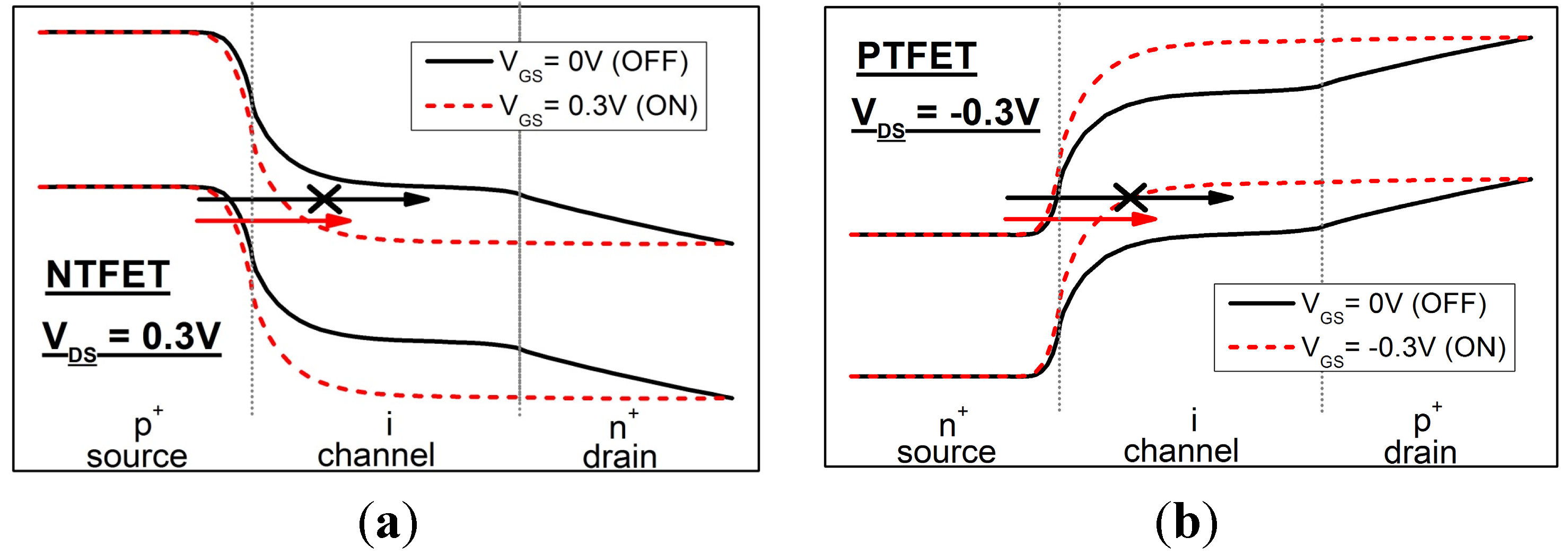
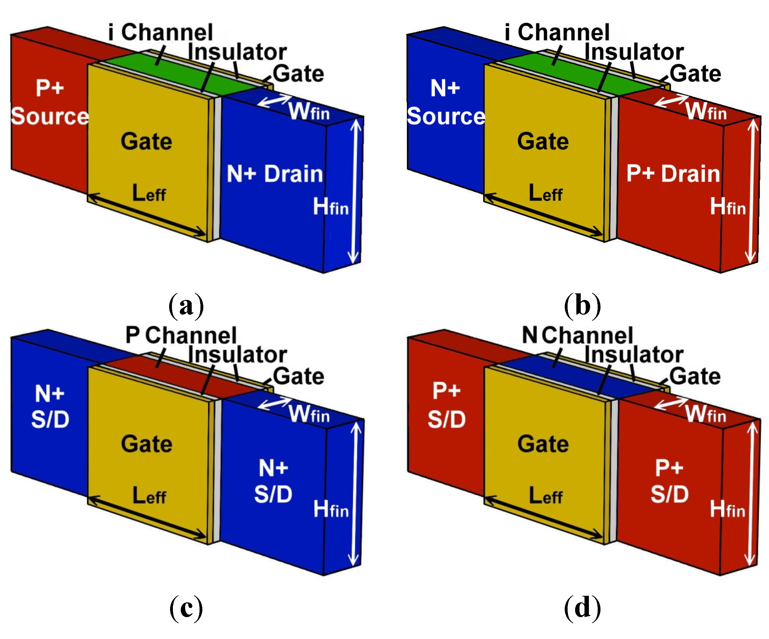
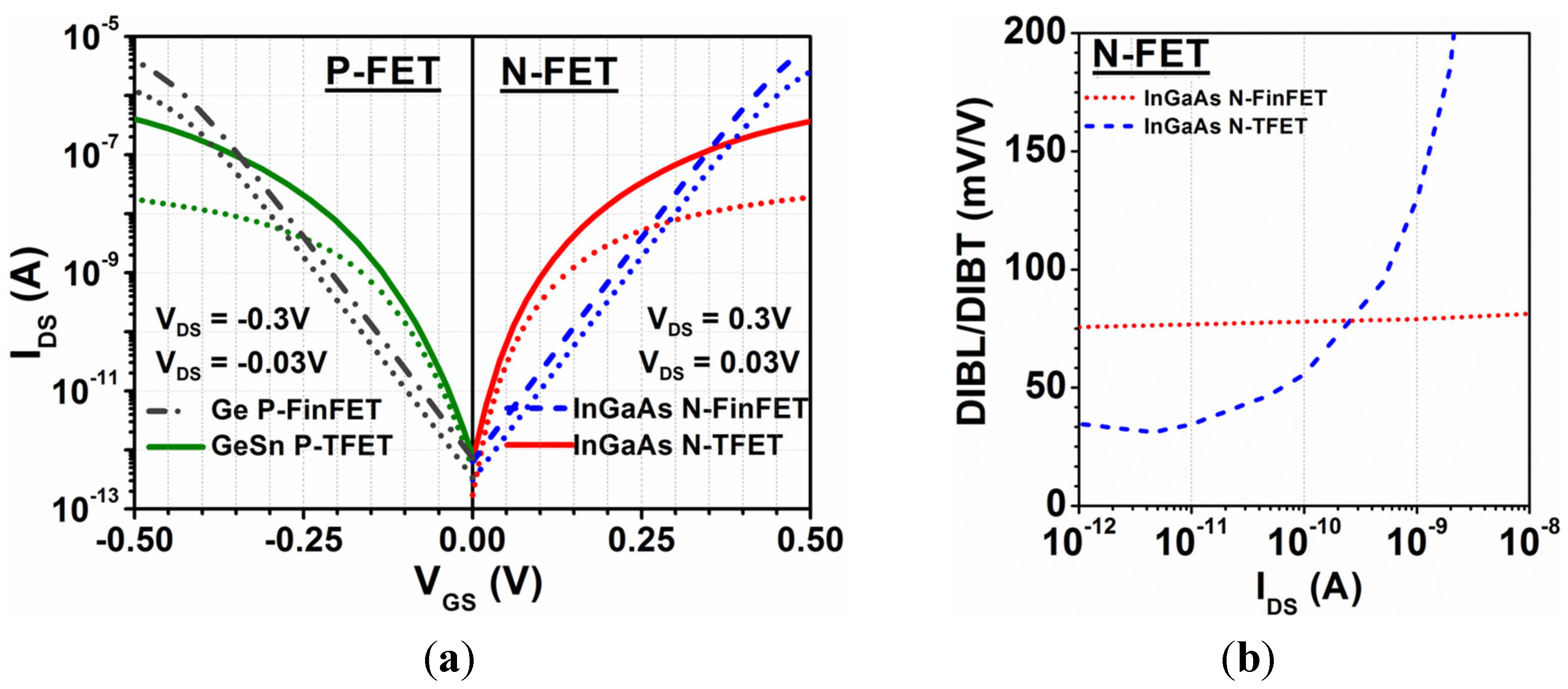
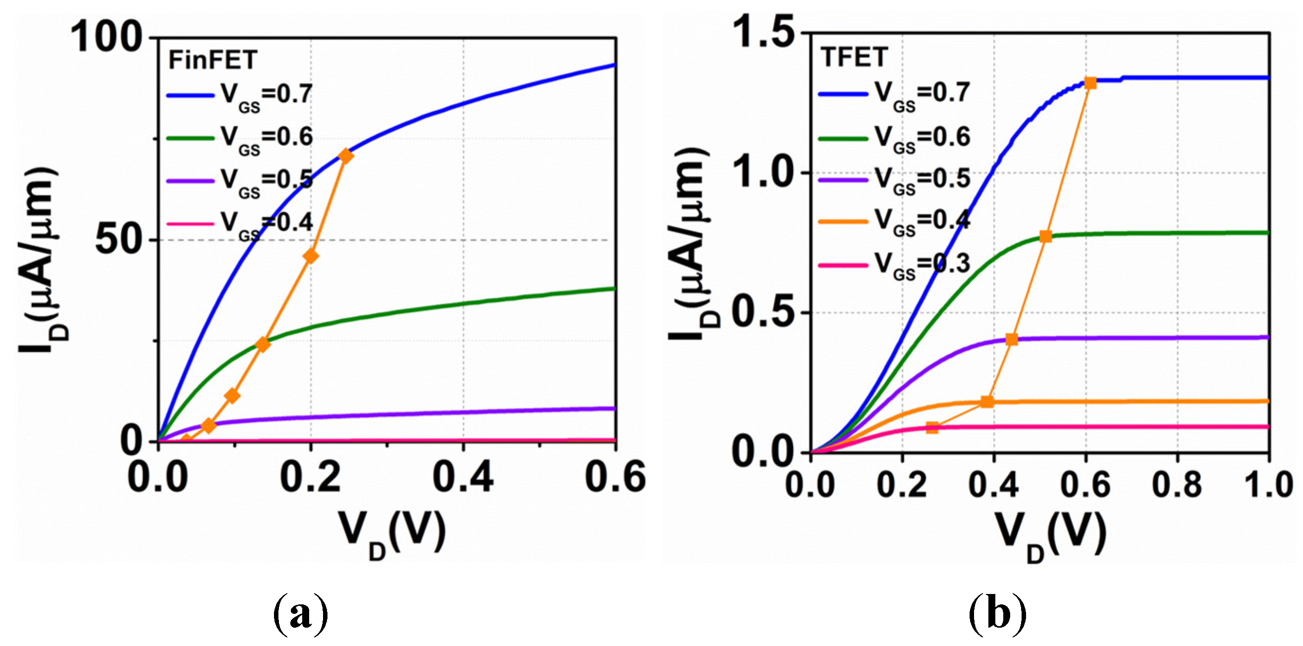
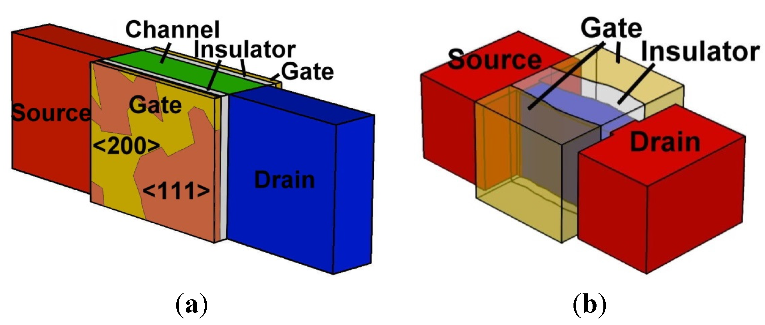
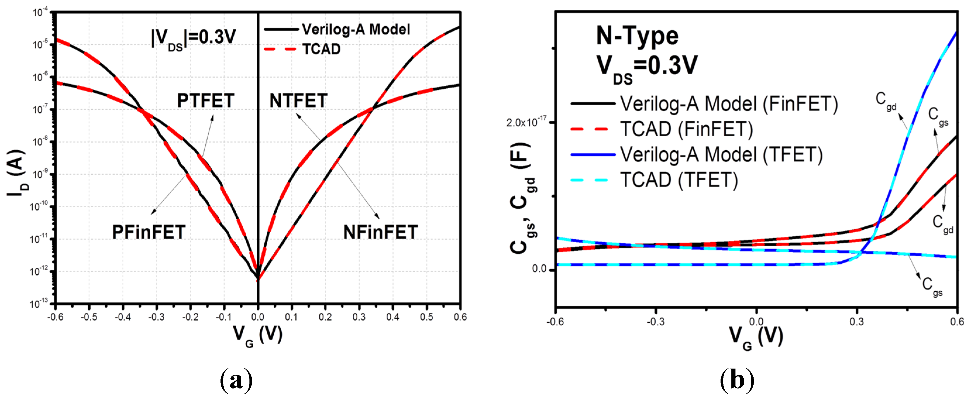
2.1. Device Structures and Characteristics

The basic TFET structure under study comprises a gated p-i-n tunnel diode under reverse bias with asymmetrical source/drain doping. For N-TFET, the source is p+ region with dominant electron conduction, the channel is gated intrinsic region, and the drain is n+ region. When N-TFET is “OFF” (VGS = 0), the valence band edge of the source is below the conduction band edge of the channel, and the band-to-band tunneling probability is low due to lack of available states in the channel region and wide barrier at source-channel junction. When N-TFET is “ON” (VGS > 0), the conduction band edge of the channel is pulled down below the valence band edge of the source, and carriers can tunnel into available empty states of the channel region. For P-TFET, the source is n+ region with dominant hole conduction, applying VGS < 0 turns P-TFET “ON”. The band diagrams of TFET in ON/OFF states are shown in Figure 1.
In this work, we consider the In0.53Ga0.47As homojunction N-TFET and Ge0.925Sn0.075 homojunction P-TFET due to their high Ion and compatible IDS-VGS characteristic [12,13]. In0.53Ga0.47As N-FinFET and Ge P-FinFET with high mobility are considered for comparison. Figure 2 shows the 3D TFET and FinFET device structures constructed for atomistic TCAD simulations. The device parameters and doping are shown in Table 1. We use the non-local band-to-band tunneling model which is applicable to arbitrary tunneling barrier with non-uniform electric field for TFET simulations [11], and the parameters used in the model are calibrated with [12,13]. Figure 3a shows the IDS-VGS characteristics of TFETs and FinFETs at VDS = 0.3 V and VDS = 0.03 V. The DIBL (drain-induced barrier lowering) and DIBT (drain-induced barrier thinning) values versus drain current for N-TFET and N-FinFET are shown in Figure 3b. DIBL for the conventional MOSFET device is estimated using the following formula in weak inversion region (subthreshold region):
DIBL =   Δ V T H Δ V D S   ( mV / V )
Figure 1. Energy band diagrams of (a) n-type and (b) p-type TFET in ON/OFF state.
Jlpea 05 00101 g001
Figure 2. Physical structures of (a) In0.53Ga0.47As homojunction N-TFET; (b) Ge0.925Sn0.075 homojunction P-TFET; (c) In0.53Ga0.47As N-FinFET and (d) Ge P-FinFET.
Jlpea 05 00101 g002
Table 1. Parameters of TFET and FinFET devices.
DevicesTFETFinFET
Leff = 25 nmWfin = 7 nmHfin = 20 nmEOT = 0.65 nm
nTFETpTFETFinFET
MaterialIn0.53Ga0.47AsGe0.925Sn0.075In0.53Ga0.47As
Nch (cm−3)undopedundoped1 × 1017
Ns (cm−3)4.5 × 10¹⁹ (p-type)2 × 10¹⁹ (n-type)1 × 10²⁰
Nd (cm−3)2 × 10¹⁷ (n-type)2 × 10¹⁷ (p-type)1 × 10²⁰
Figure 3. (a) IDS-VGS characteristics at VDS = 0.3 V and VDS = 0.03 V of In0.53Ga0.47As N-TFET, Ge0.925Sn0.075 P-TFET, In0.53Ga0.47As N-FinFET and Ge P-FinFET; (b) DIBL and DIBT value versus drain current for In0.53Ga0.47As N-TFET and N-FinFET.
Jlpea 05 00101 g003
In TFET, the drain bias also plays a role in enhancing the drain current due to the drain bias induced source-channel tunneling barrier thinning effect. However, as the physics-based method for extracting the threshold voltage of TFET is still under investigation, there is no clear definition for DIBT extraction analogous to DIBL in FiFET device. Hence, for first-order approximation for estimating DIBT in TFET device, we draw the DIBT as a function of drain to source current shown in Figure 3b. As can be seen, the DIBT for TFET shows non-monotonic behavior compared with the FinFET counterpart and increases rapidly as the drain to source current increases beyond 0.2 nA. This is because TFET has smaller threshold voltage (using the constant current defined Vth) and enters the saturation region earlier than the FinFET which is in the weak inversion region with DIBL roughly around 80 mV/V.
Figure 4 shows the output characteristics for TFET and FinFET devices. As shown, TFET device shows larger VDSAT [14] as indicated in rhombus symbol due to the fact that TFET can be regarded as a source-channel tunneling junction in series with a resistor (i.e., channel resistance), hence exhibiting an upward-concaved shape in the triode-like region (analogous to FinFET). At moderate and high VDS, TFET provides a better (flatter) saturation characteristic due to reduced carriers in the channel region, and the electric field from the drain side cannot penetrate into the source-channel tunnel junction, so the current increases slowly. For FinFET device, no obvious saturation is observed due to more severe short-channel effect.
Figure 4. IDS-VDS characteristics at various VGS bias for (a) FinFET and (b) TFET device with the rhombus symbol showing the extrated VDSAT.
Jlpea 05 00101 g004

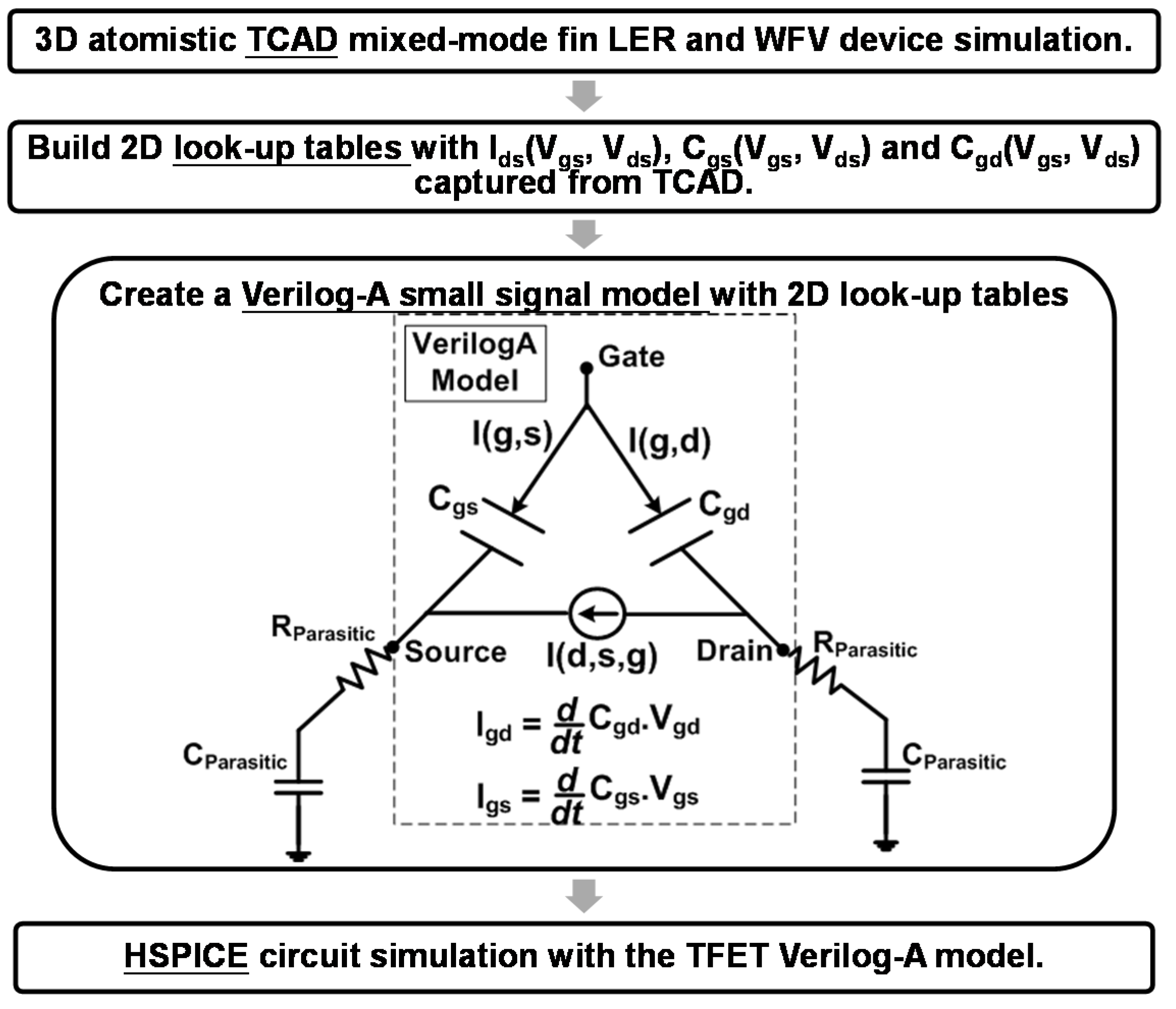
2.2. Simulation Methodology

To assess WFV, we use the Vonoroi grain pattern [15] for TiN gate material, which has two different grain orientations <200> and <111> with the probability of 60% and 40%, respectively, as shown in Figure 5a by the yellow and orange regions, and the relevant parameters are shown in Table 2. To assess fin LER, the rough line edge patterns are generated by Fourier synthesis approach [16] with correlation length (Λ) = 20 nm and root-mean-square amplitude (Δ) = 1.5 nm as shown in Figure 5b. We analyze the impacts of WFV and fin LER on devices using 3D atomistic TCAD mixed-mode Monte-Carlo simulations with 100 samples, respectively.
Figure 5. Examples of structures with (a) WFV and (b) fin LER.
Jlpea 05 00101 g005
Table 2. Parameters for WFV simulations.
Gate Material = TiNGrain Size = 5 nm
Work function (eV)Nominal<200> (60%)<111> (40%)
InGaAs N-TFET4.534.614.41
GeSn P-TFET4.824.94.7
InGaAs N-FinFET4.884.964.76
Ge P-FinFET4.274.354.15
TCAD mixed-mode simulations for complex circuits with large transistor counts face the challenges of computation resources, prohibitively long simulation times and convergence problems. To overcome these obstacles, look-up table based Verilog-A model has been employed for TFET circuit simulations in some studies [2,4]. However, these works on TFET circuits employed simple parameter sensitivity methods [2,9], and these sensitivity-based Verilog-A models cannot accurately describe the physical non-uniformities and variability. In this work, we adopt physics-based assessment to account for variability at device and circuit level. The flow chart for physics-based small signal Verilog-A model generation is shown in Figure 6. The transfer characteristics of TFET and FinFET devices and their variability with WFV and fin LER are extracted from atomistic 3D TCAD device simulations with IDS (VGS, VDS), Cgs (VGS, VDS) and Cgd (VGS, VDS) characteristics across voltage range of interest to build two-dimensional Verilog-A look-up tables. The Verilog-A models of devices with random variations are then employed in HSPICE circuit simulations. The calibrations of Verilog-A models with TCAD results on I-V, C-V characteristics of the nominal cases for TFET and FinFET devices are shown in Figure 7. The almost exact agreements can be clearly seen.
Figure 6. Flowchart for HSPICE look-up table based Verilog-A model generation from atomistic 3D TCAD simulations [2,4].
Jlpea 05 00101 g006
Figure 7. Calibrations of Verilog-A models with TCAD results on (a) I-V and (b) C-V charcteristics of the nominal cases for TFET and FinFET deivces at VDS = 0.3 V.
Jlpea 05 00101 g007

3. Device Variability Due to WFV and Fin LER

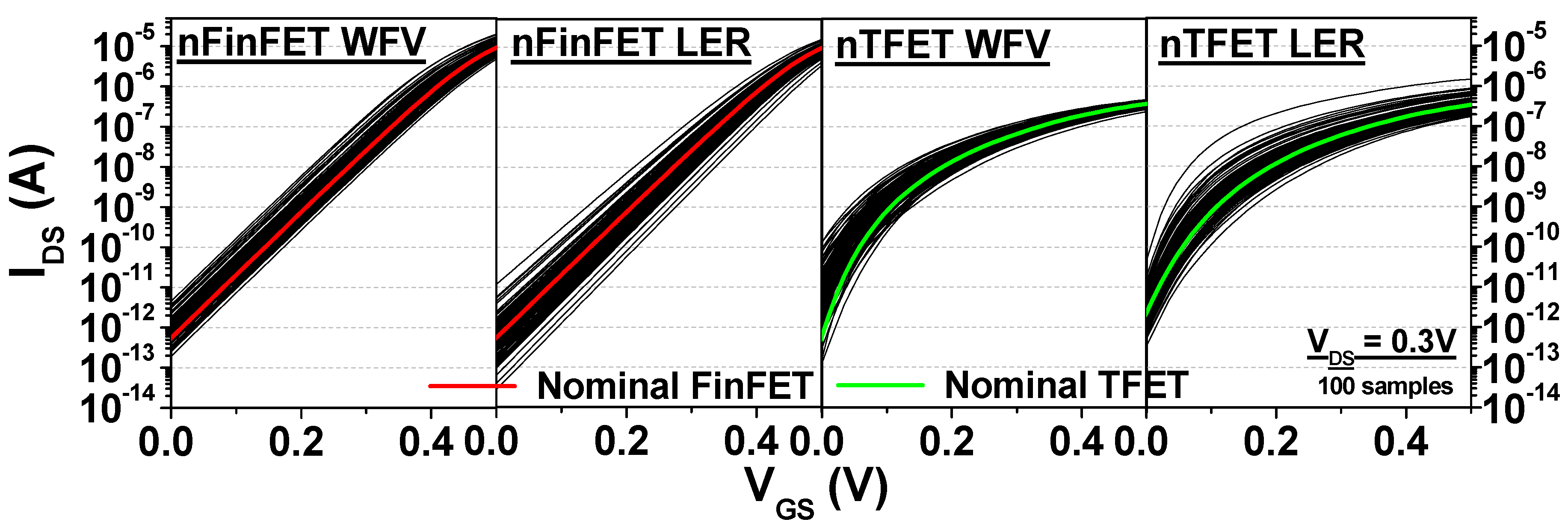
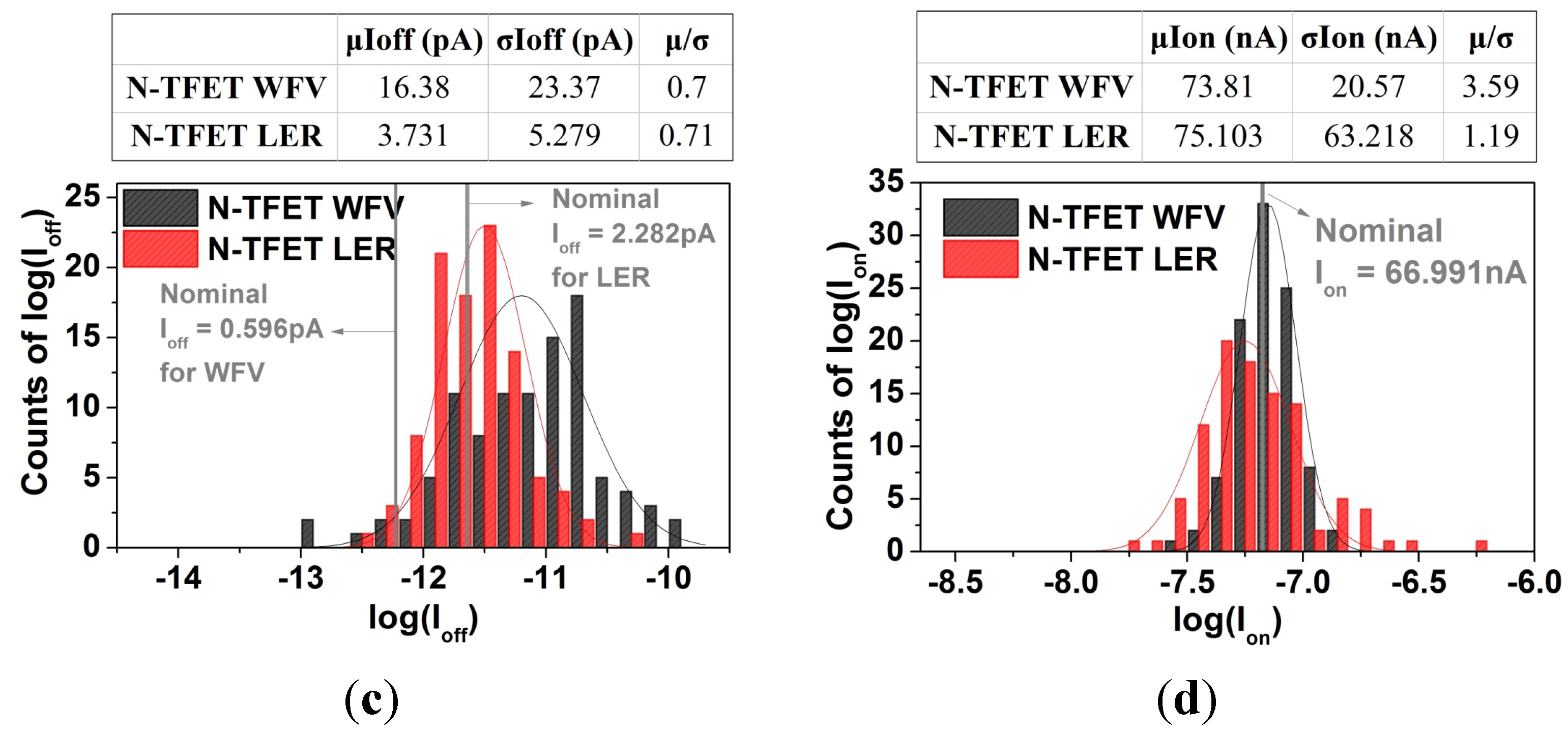
3.1. Ioff and Ion Variability
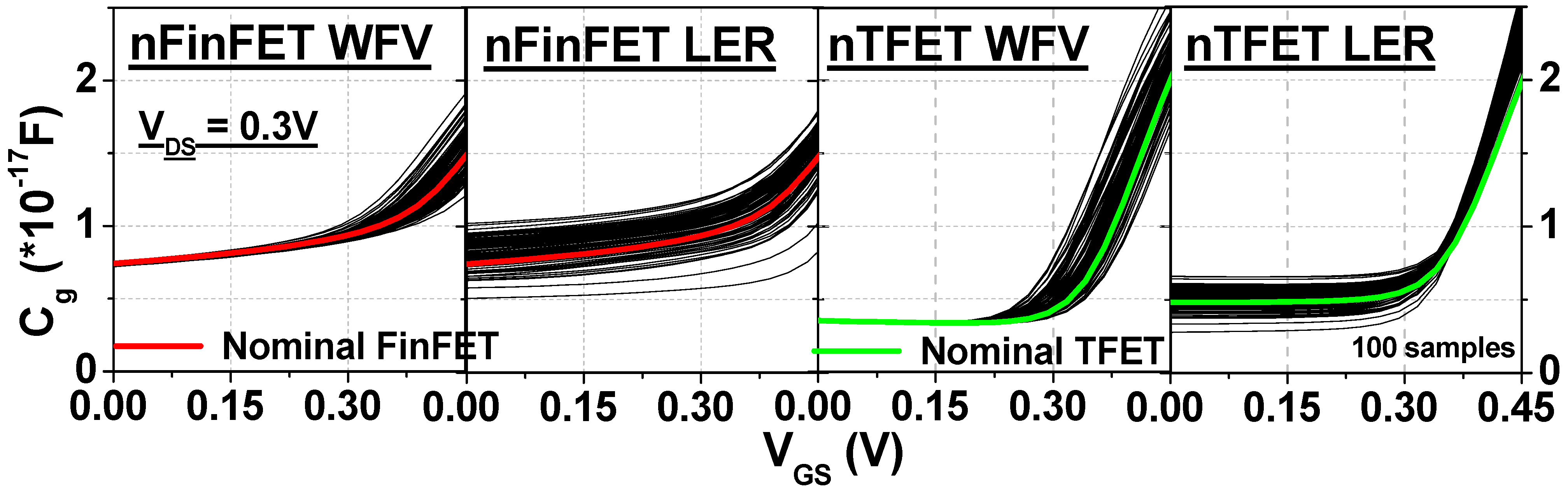
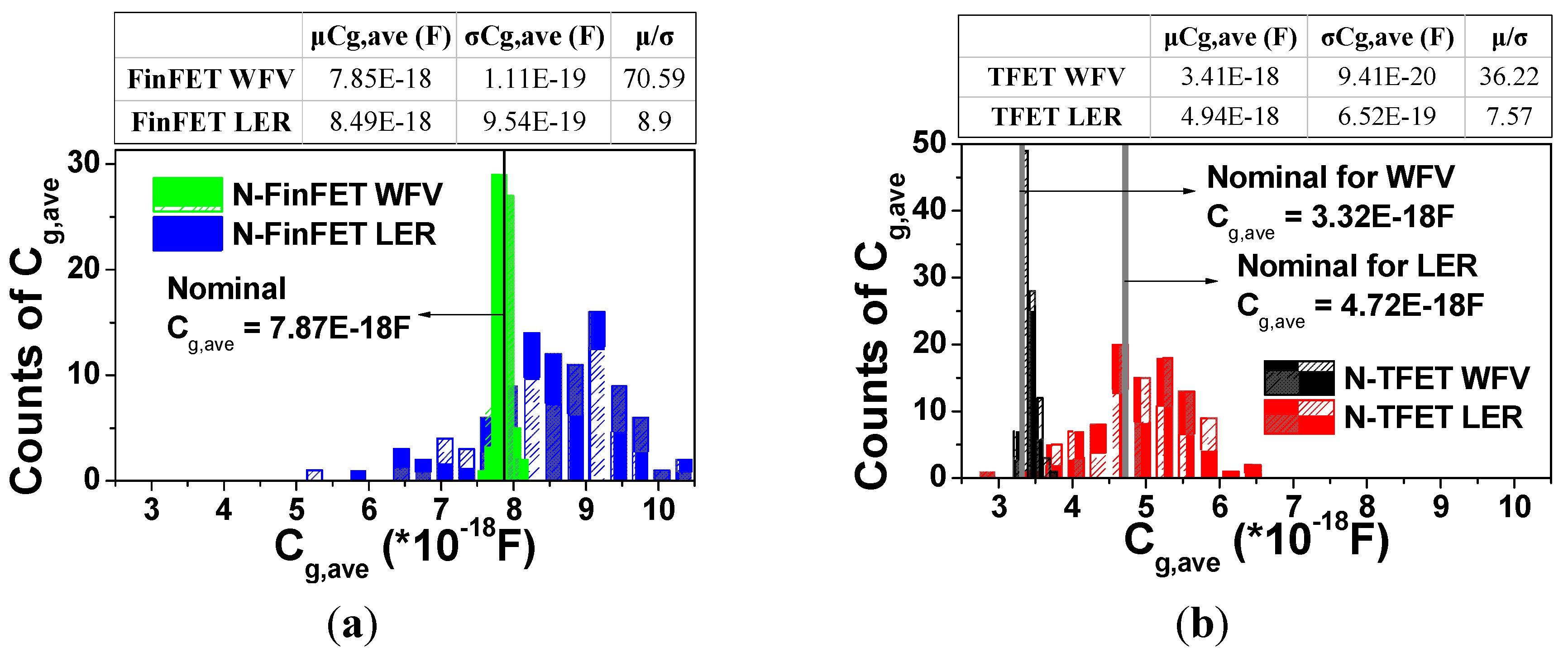
Figure 8 shows the impacts of WFV and fin LER on IDS-VGS dispersions of TFET and FinFET devices at VDS = 0.3 V. Figure 9 illustrates the probability distributions of Ion (IDS at VDS = VGS = 0.3 V) and Ioff (IDS at VDS = 0.3 V and VGS = 0 V). Note that, for TFET variability, the different structure constructs used for WFV and fin LER lead to slightly different nominal IDS-VGS curves. Therefore, the corresponding probability distributions show two nominal values. The mean values (μ), standard deviations (σ) and the ratio of the mean-to-standard deviation (μ/σ) are listed in the table with the figures.
For FinFETs, the Vt is a linear function of gate WF, WFV causes a Vt shift of IDS-VGS curves in subthreshold region with almost equal subthreshold swing (S.S.), therefore the Ion and Ioff probability distributions are similar. On the other hand, fin LER influences the effective fin width and electrostatic integrity, thus impacting both Vt and S.S., so the Ion and Ioff probability distributions are quite different. As can be seen, both the μ/σ of Ion and Ioff are worse with fin LER than WFV, especially for Ioff.
Figure 8. Simulated IDS-VGS characteristics at VDS = 0.3 V for TFET and FinFET with WFV and fin LER.
Jlpea 05 00101 g008
Figure 9. Probability distribution of (a) log(Ioff); (b) log(Ion) for FinFET and (c) log(Ioff); (d) log(Ion) for TFET at VDS = 0.3 V considering WFV and fin LER.
Jlpea 05 00101 g009aJlpea 05 00101 g009b
For TFETs, the Ioff distribution with WFV is boarder (worse) than that with fin LER since WFV leads to fluctuation in the energy bands and alters the critical tunneling path, and the effect decreases with increasing VGS. The metal grains with various WF form the up and down energy bands that boost the band-to-band generation, resulting in large Ioff distribution. Therefore, the variability of Ioff is larger than Ion, and the correlation between Ion and Ioff is weak. On the other hand, for fin LER, both Ion and Ioff are degraded as fin width (WFin) increases due to the weaker electrostatic control of the channel from both gates, and the degradations of Ion and Ioff track WFin with exponential-like behavior, especially for Ioff which dramatically increases with decreasing WFin. Comparing with fin LER, the μ/σ (Ion) of WFV is better, and the μ/σ (Ioff) of WFV is comparable to LER. In addition, WFV causes larger σ (Ioff) than LER. Overall, comparing FinFET and TFET, the impacts due to WFV on Ion and Ioff are quite different. The μ/σ (Ioff) of TFET is worse while μ/σ (Ion) of TFET is better. In addition, the Ioff distribution of TFET skews to high values, and not as symmetrical as the Ioff distribution for FinFET, resulting in larger μ (Ioff). On the other hand, the variation of TFET considering fin LER is slight better than FinFET.

3.2. Cg Variability

Figure 10 shows the impacts of WFV and fin LER on Cg-VGS dispersions of TFET and FinFET devices at VDS = 0.3 V. Figure 11 illustrates the probability distributions of Cg,ave (the average capacitance across the gate-bias range from 0 to VDD = 0.3 V) at VDS = VDD. For both TFET and FinFET, the Cg variation by WFV becomes more significant at larger VGS. In contrast, the variation due to fin LER is more severe when VGS is small. Note that Cg,ave is extracted only for the range from VGS = 0 V to 0.3 V. The μ/σ (WFV) are much better compared with μ/σ (LER). For TFET with WFV and FinFET with fin LER, the Cg,ave skews to high values, resulting in larger μ than the nominal cases.
Figure 10. Simulated Cg-VGS characteristics at VDS = 0.3 V for TFET and FinFET with WFV and fin LER.
Jlpea 05 00101 g010
Figure 11. Probability distribution of Cg,ave for (a) FinFET and (b) TFET at VDS = 0.3 V considering WFV and fin LER.
Jlpea 05 00101 g011

4. Impacts of WFV and Fin LER on CLA Circuits

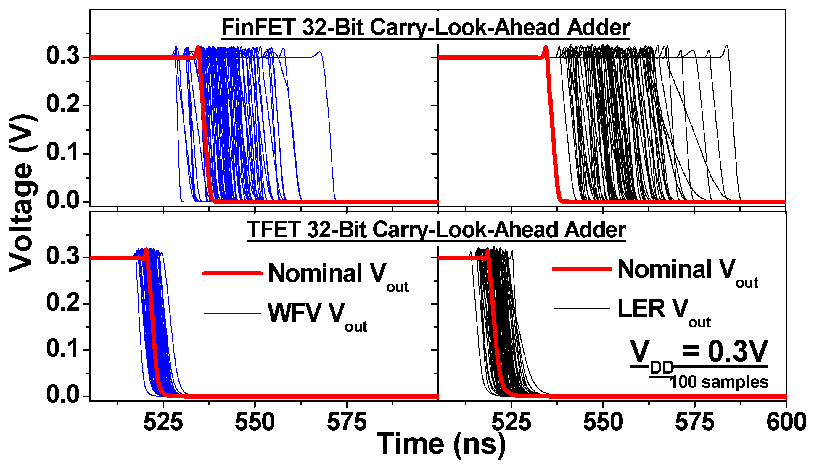
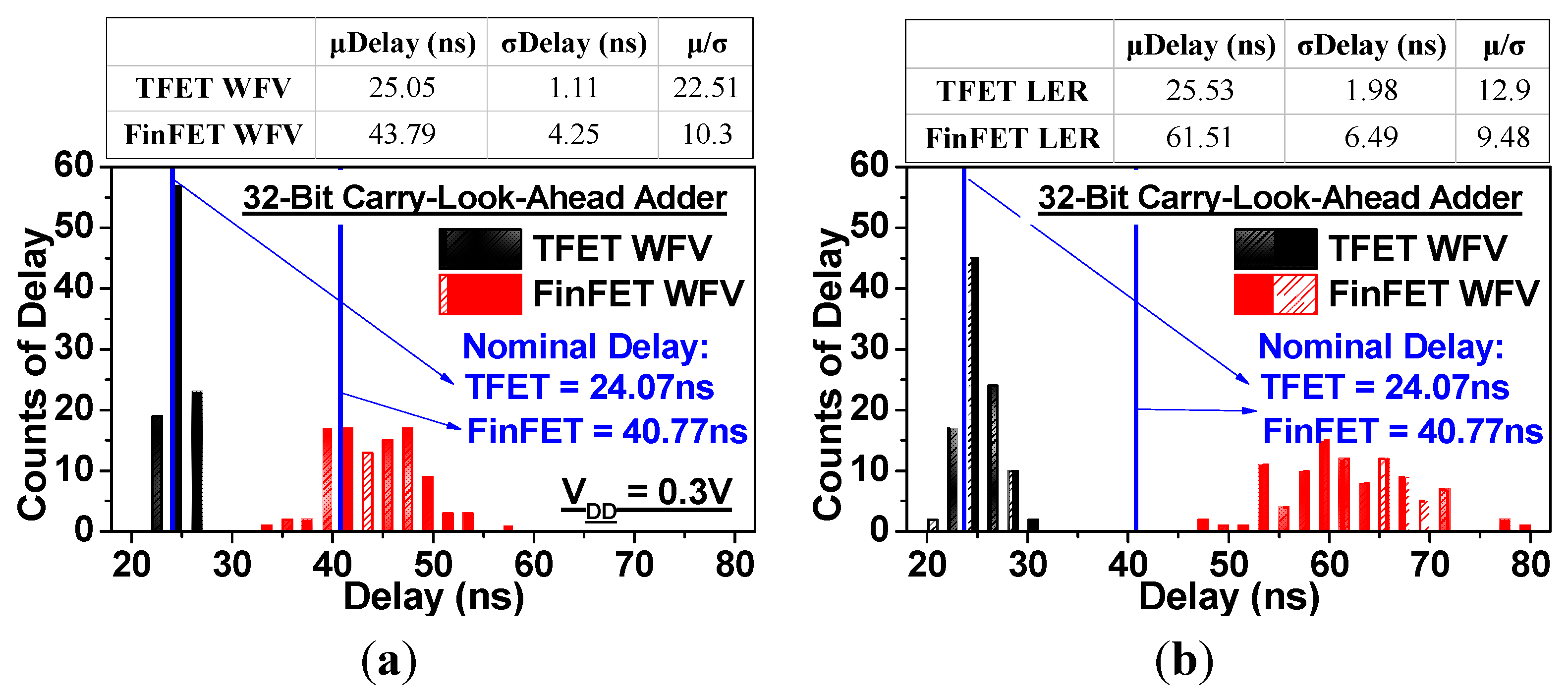
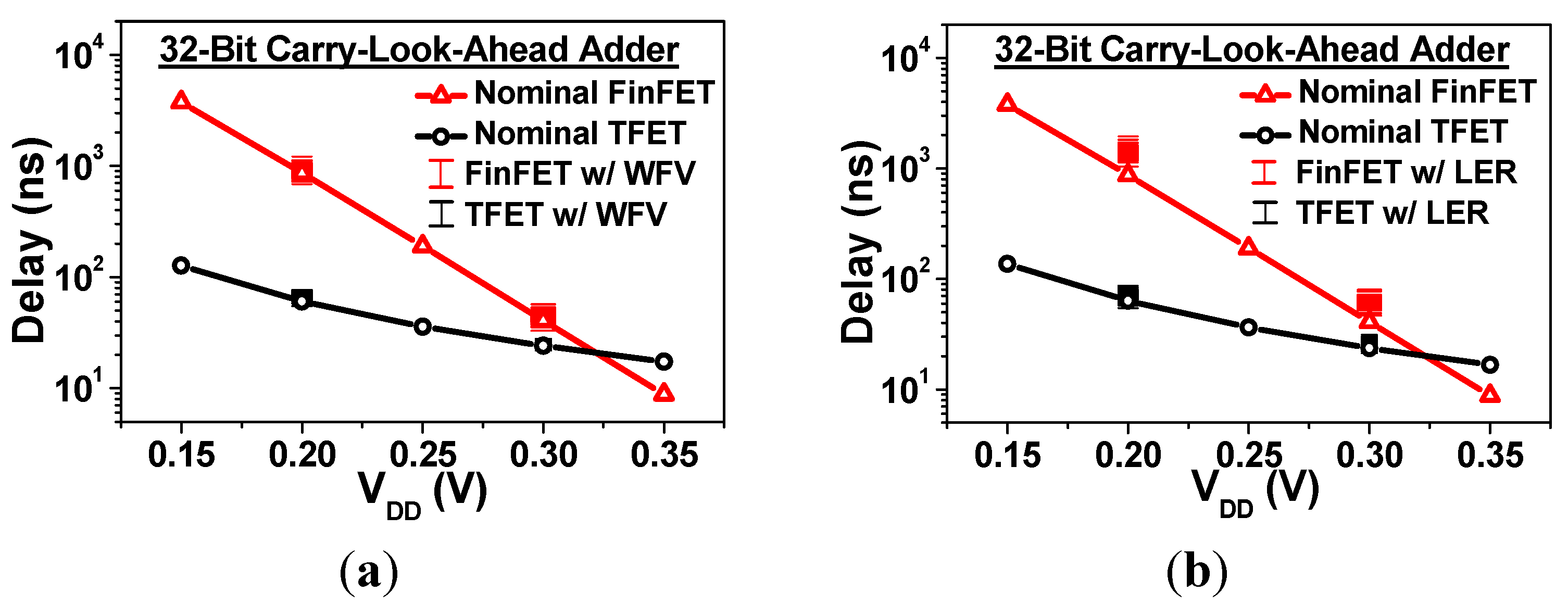
4.1. Delay Variability

The switching delay is commonly calculated as τ = (Cg VDD)/Ion. Due to the strong bias dependence of gate capacitance (Cg), the average capacitance (Cg,ave) across the gate-bias range from 0 to VDD (0.3 V in this case) at VDS = VDD is determined for approximation: τ = (Cg,ave VDD)/Ion.
The transient waveforms and the probability distributions of delays for 32-bit CLA of TFET and FinFET with WFV and fin LER are shown in Figure 12 and Figure 13. As can be seen, the μ/σ (Delay) of TFET is better than FinFET in both cases (with WFV and fin LER). For both TFET and FinFET, the μ/σ (WFV) is better than μ/σ (LER). The variability of delay correlates with aforementioned Ion and Cg,ave variations in Section 3. The smaller Ion of FinFET significantly degrades its μ/σ (Delay).
Figure 12. Transient waveforms of 32-bit CLA for TFET and FinFET at VDD = 0.3 V considering WFV and fin LER.
Jlpea 05 00101 g012
Figure 13. Probability distribution of delay for 32-bit CLA with (a) WFV; (b) fin LER for TFET and FinFET at VDD = 0.3 V.
Jlpea 05 00101 g013
Figure 14 presents the delay for 32-bit CLA of TFET and Fin FET versus VDD from 0.15 V to 0.35 V for the nominal cases and the cases considering WFV and fin LER (at 0.2 V and 0.3 V). The delay variability of all cases becomes worse with decreasing VDD due to decreasing IDS. The delay and its variability of TFET are significantly better than FinFET at low VDD due to its larger IDS and smaller Cg,ave variation compared with FinFET.
Figure 14. Delay for 32-bit CLA of TFET and FinFET versus VDD from 0.15 V to 0.35 V for the nominal cases and the cases considering (a) WFV and (b) fin LER (0.2 V and 0.3 V).
Jlpea 05 00101 g014

4.2. PDP Variability

PDP is a figure of merit representing the power-performance trade-off. At a given operation frequency, PDP is calculated as PDP = (Cg V2DD f) × tdelayCg,ave V2DD f tdelay. If the frequency is scaled up to the maximum operation frequency (i.e., f = 1/tdelay), then PDP = (Cg V2DD) would represent the energy dissipated in a switching event.
The probability distributions of PDP 32-bit CLA of TFET and FinFET for the nominal cases and the cases with WFV and fin LER are shown in Figure 15. The μ/σ (WFV) is better than μ/σ (LER) for both TFET and FinFET, and the distributions of TFET with WFV and that of FinFET with fin LER skew to larger values.
Figure 15. Probability distribution of PDP for 32-bit CLA with (a) WFV; (b) fin LER for TFET and FinFET at VDD = 0.3 V.
Jlpea 05 00101 g015
Figure 16 shows the PDP for 32-bit CLA of TFET and FinFET versus VDD from 0.15 V to 0.35 V for the nominal cases and the cases considering WFV and fin LER (at 0.2 V and 0.3 V). As can be seen, TFET PDP is much better than FinFET at low VDD due to the fact that Cg,ave variation of FinFET is larger and skewed to high values compared with TFET. Notice that the PDP of TFET is still better than FinFET considering random variations.
Figure 16. PDP for 32-bit CLA of TFET and FinFET versus VDD from 0.15 V to 0.35 V for the nominal cases and the cases considering (a) WFV and (b) fin LER (0.2 V and 0.3 V).
Jlpea 05 00101 g016

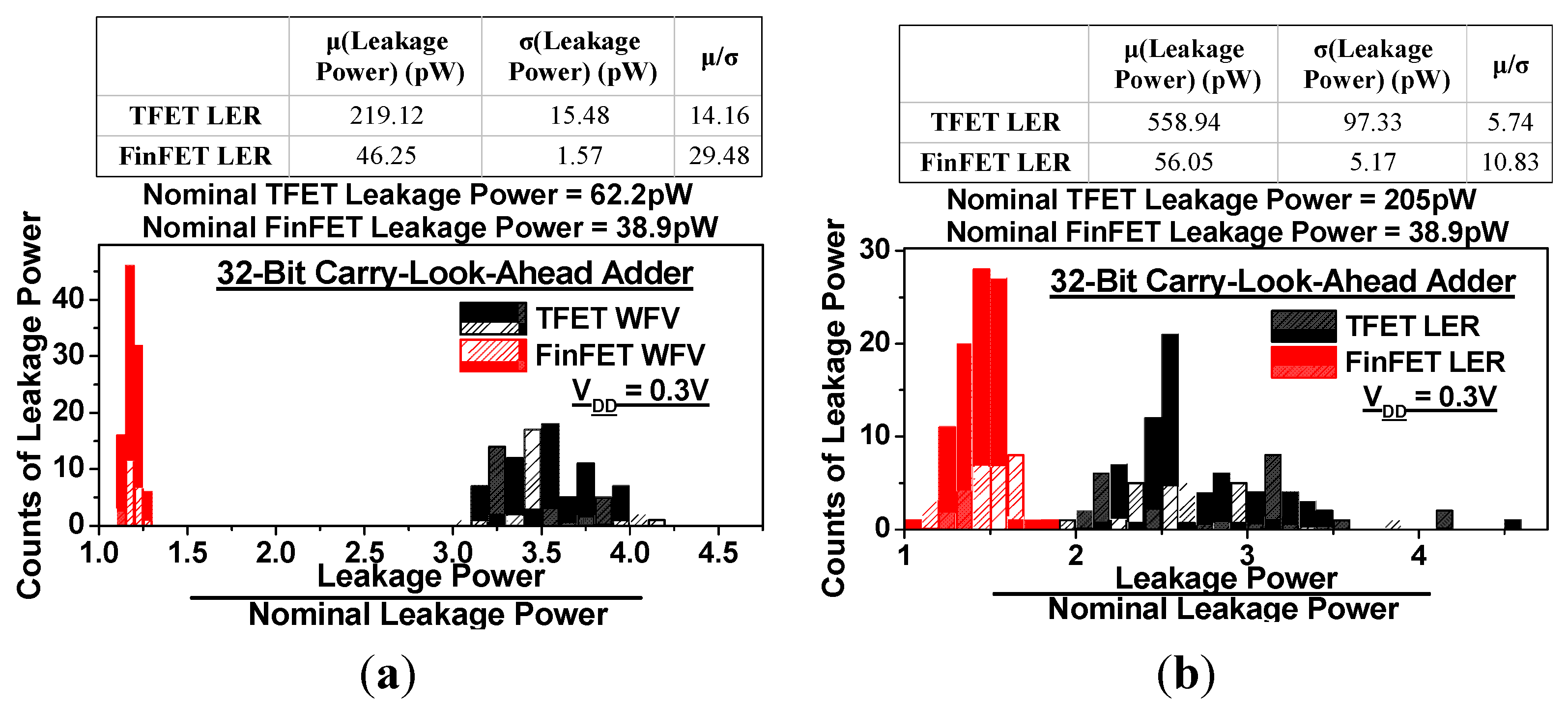
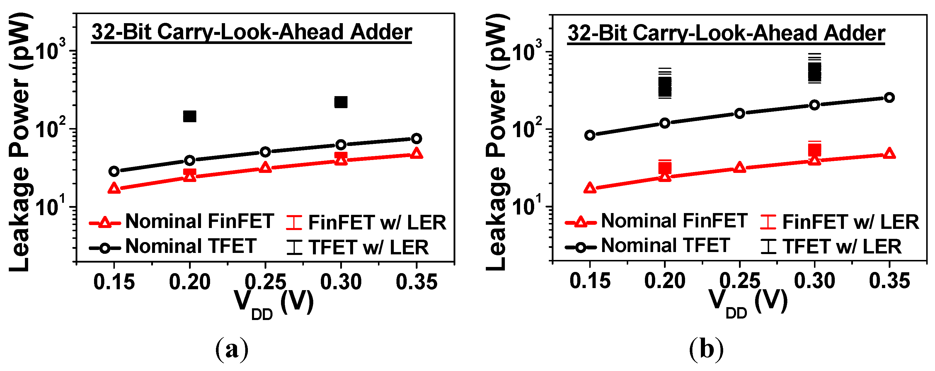
4.3. Leakage Power Variability

The probability distributions of leakage power for 32-bit CLA of TFET and FinFET for the nominal cases and the cases with WFV and fin LER at VDD = 0.3 V are shown in Figure 17. The leakage power variation of TFET with both variation sources are much worse than FinFET, and the distributions skew to larger values, especially under WFV. This correlates to aforementioned Ioff variations in Section 3.
Figure 17. Probability distribution of leakage power for 32-bit CLA with (a) WFV; (b) fin LER for TFET and FinFET at VDD = 0.3 V.
Jlpea 05 00101 g017
Figure 18 shows the leakage power for 32-bit CLA of TFET and FinFET versus VDD from 0.15 V to 0.35 V for the nominal cases and the cases considering WFV and fin LER (at 0.2 V and 0.3 V). As the operating voltage is reduced, the leakage power decreases. Notice that the increase of leakage power by random variations is more significant than the influence by operating voltage for TFET.
Figure 18. Leakage power for 32-bit CLA of TFET and FinFET versus VDD from 0.15 V to 0.35 V for the nominal cases and the cases considering (a) work function variation (WFV) and (b) fin Line-Edge-Roughness (fin LER) (0.2 V and 0.3 V).
Jlpea 05 00101 g018

5. Conclusions

We investigate and compare the impacts of WFV and fin LER on TFET and FinFET Ion, Ioff and Cg,ave using atomistic 3D TCAD simulations with calibrated model and device parameters. Our studies indicate that considering WFV, FinFET has comparable Ion and Ioff variability while TFET has smaller Ion variability and larger Ioff variability. In addition, the band diagram dispersion caused by WFV increases the band-to-band generation for TFET in “OFF” state, leading to skewed Ioff distribution to larger values. On the other hand, the impact of fin LER is similar for TFET and FinFET, resulting in comparable Ion and Ioff variability. The Cg,ave variability is worse with fin LER compared with WFV for both TFET and FinFET.
Using Verilog-A device models extracted from atomistic 3D TCAD simulations to capture the physical non-uniformities and variability, HSPICE circuit simulations are performed to assess the impacts of WFV and fin LER on TFET and FinFET 32-bit CLA. The results show that at low operating voltage (<0.3 V), the delay and PDP of TFET CLA are significantly better than the FinFET counterparts, even under the impacts of WFV and LER. However, the variability of leakage power for TFET CLA is worse than FinFET CLA, especially with WFV. The leakage power distribution of TFET CLA skews to larger values due to its worse Ioff variability.

Acknowledgments

This work was supported in part by the Ministry of Science and Technology in Taiwan under Contract MOST 103-2221-E-009-196-MY2, and by the Ministry of Education in Taiwan under the ATU Program. The authors thank the National Center for High-Performance Computing in Taiwan for the software and facilities.

Author Contributions

Author Yin-Nien Chen contributed to the literature search and coordinated the the research, discussion and prepared the manuscript. Author Chien-Ju Chen contributed to the simulated works, discussion and the manuscript. Author Dr. Ming-Long Fan and Dr. Vita Pi-Ho Hu contributed to the technical suggestions and discussion. Author Prof. Pin Su guided this research work and contributed to technical discussions on device part about the impacts of intrinsic variations on TFET and FinFET devices. Author Prof. Ching-Te Chuang guided this research work and contributed to technical discussions on the circuit part and paper writing by reviewing all the results presented in this work and revising the technical writing and formatting of the manuscript.

Conflicts of Interest

The authors declare no conflict of interest.

References

  1. Ionescu, A.M.; Riel, H. Tunnel field-effect transistors as enrgy-efficient electronics switches. Nature 2011, 479, 329–337. [Google Scholar] [CrossRef] [PubMed]
  2. Saripalli, V.; Datta, S.; Narayanan, V.; Kulkarni, J.P. Variation-tolerant ultra low-power heterojunction tunnel FET SRAM design. In Proceedings of the 2011 IEEE/ACM International Symposium on Nanoscale Architectures (NANOARCH), San Diego, CA, USA, 8–9 June 2011; pp. 45–52.
  3. Cotter, M.; Liu, H.C.; Datta, S.; Narayanan, V. Evaluation of tunnel FET-based flip-flop designs for low power, high performance applications. In Proceedings of the 2013 14th International Symposium on Quality Electronic Design (ISQED), Santa Clara, CA, USA, 4–6 March 2013; pp. 430–437.
  4. Datta, S.; Bijesh, R.; Liu, H.; Mohata, D.; Narayanan, V. Tunnel transistors for energy efficient computing. In Proceedings of the 2013 IEEE International Reliability Physics Symposium (IRPS), Anaheim, CA, USA, 14–18 April 2013; pp. 6A.3.1–6A.3.7.
  5. Leung, G.; Chui, C.O. Stochastic Variability in Silicon Double-Gate Lateral Tunnel Field-Effect Transistors. IEEE Trans. Electron Devices 2012, 60, 84–91. [Google Scholar] [CrossRef]
  6. Fan, M.L.; Hu, V.P.H.; Chen, Y.N.; Su, P.; Chuang, C.T. Analysis of Single-Trap-Induced Random Telegraph Noise and its Interaction With Work Function Variation for Tunnel FET. IEEE Trans. Electron Devices 2013, 60, 2038–2044. [Google Scholar] [CrossRef]
  7. Choi, K.M.; Choi, W.Y. Work-function variation effects of tunneling field-effect transistors (TFETs). IEEE Trans. Electron Device Lett. 2013, 34, 942–944. [Google Scholar] [CrossRef]
  8. Damrongplasi, N.; Kim, N.S.; Shin, H.C.; Liu, T.J.K. Impact of Gate Line-Edge Roughness (LER) vs. Random Dopant Fluctuations (RDF) on Germanium-Source Tunnel FET Performance. IEEE Trans. Nanotechnol. 2013, 12, 1061–1067. [Google Scholar] [CrossRef]
  9. Avci, U.E.; Rios, R.; Kuhn, K.J.; Young, I.A. Comparison of performance, switching energy and process variations for the TFET and MOSFET in logic. In Proceedings of the 2011 Symposium on VLSI Technology (VLSIT), Honolulu, HI, USA, 14–16 June 2011; pp. 124–125.
  10. Saripalli, V.; Mishra, A.; Datta, S.; Narayanan, V. An energy-efficient heterogeneous CMP based on hybrid TFET-CMOS cores. In Proceedings of the 48th ACM/EDAC/IEEE on Design Automation Conference (DAC), New York, NY, USA, 5–9 June 2011; pp. 729–734.
  11. Sentaurus TCAD Manual; Sentaurus Device: Mountain View, CA, USA, 2011.
  12. Liu, L.; Mohata, D.K.; Datta, S. Scaling Length Theory of Double-Gate Interband Tunnel Field-Effect Transistors. IEEE Trans. Electron Devices 2012, 59, 902–908. [Google Scholar] [CrossRef]
  13. Kotlyar, R.; Avci, U.E.; Cea, S.; Rios, R.; Linton, T.D.; Kuhn, K.J.; Young, I.A. Bandgap engineering of group IV materials for complementary n and p tunneling field effect transistors. Appl. Phys. Lett. 2013, 102, 106–113. [Google Scholar] [CrossRef]
  14. Pal, A.; Sachid, A.B.; Gossner, H.; Rao, V.R. Insights into design and optimization of TFET devices and circuits. IEEE Trans. Electron Devices 2011, 58, 1045–1053. [Google Scholar] [CrossRef]
  15. Chou, S.H.; Fan, M.L.; Su, P. Investigation and Comparison of Work Function Variation for FinFET and UTB SOI Devices Using a Voronoi Approach. IEEE Trans. Electron Devices 2013, 60, 1485–1489. [Google Scholar] [CrossRef]
  16. Asenov, A.; Kaya, S.; Brown, A.R. Intrinsic parameter fluctuations in decananometer MOSFETs introduced by gate line edge roughness. IEEE Trans. Electron Devices 2003, 50, 1254–1260. [Google Scholar] [CrossRef]

