
Extensionless UTBB FDSOI Devices in Enhanced Dynamic Threshold Mode under Low Power Point of View †

Abstract
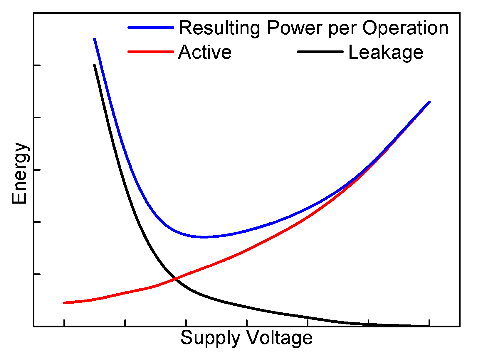
:1. Introduction

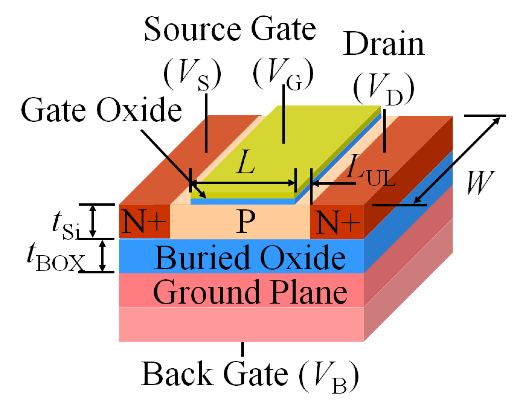
2. Device Description

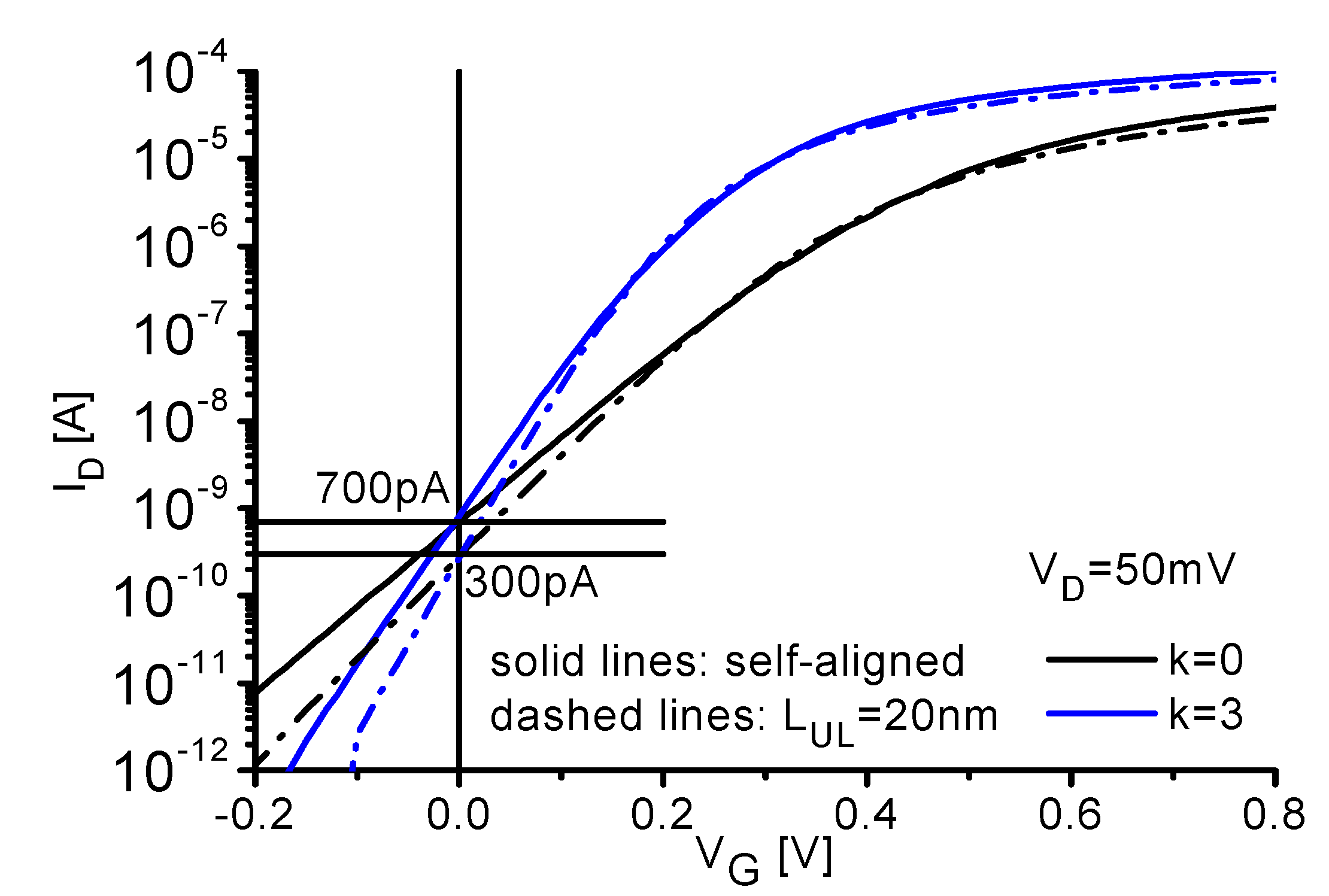
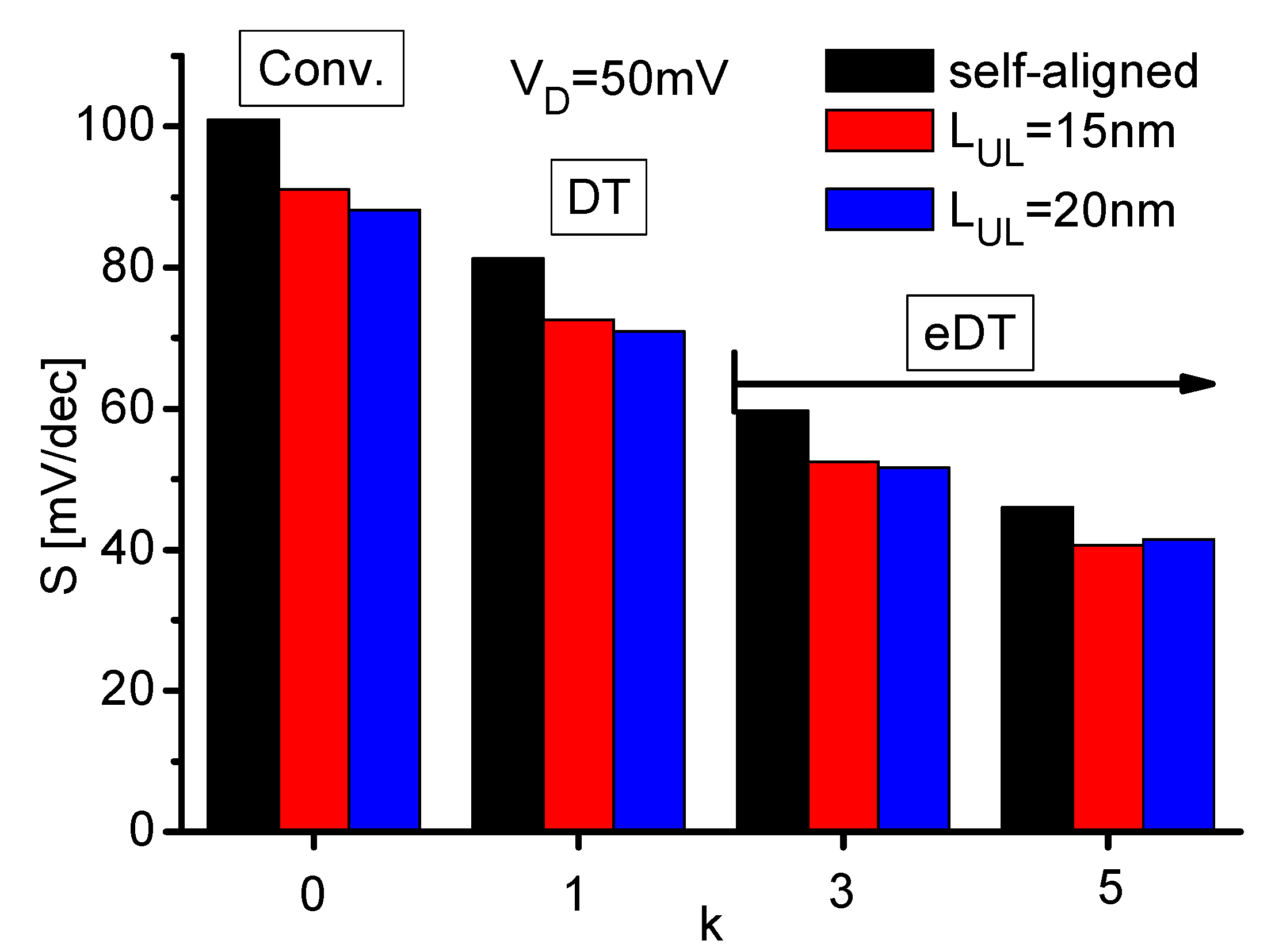
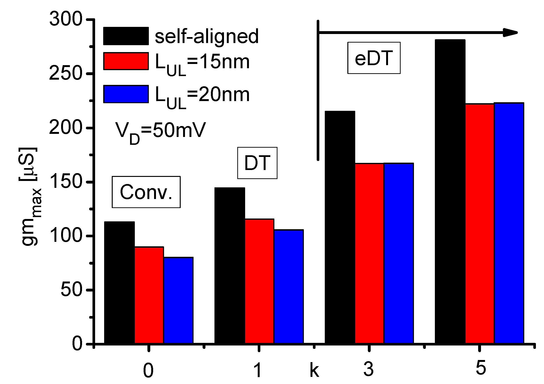
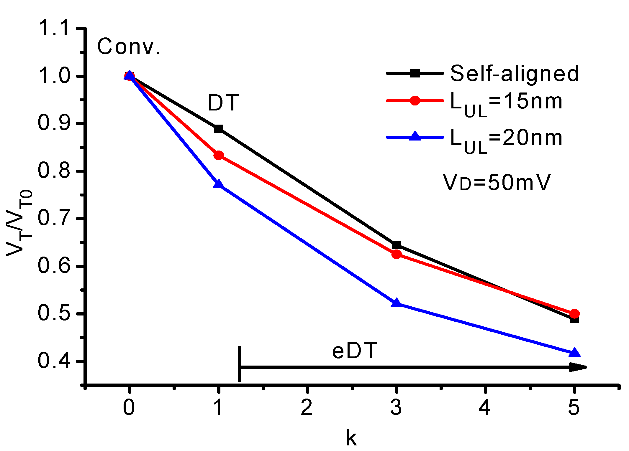
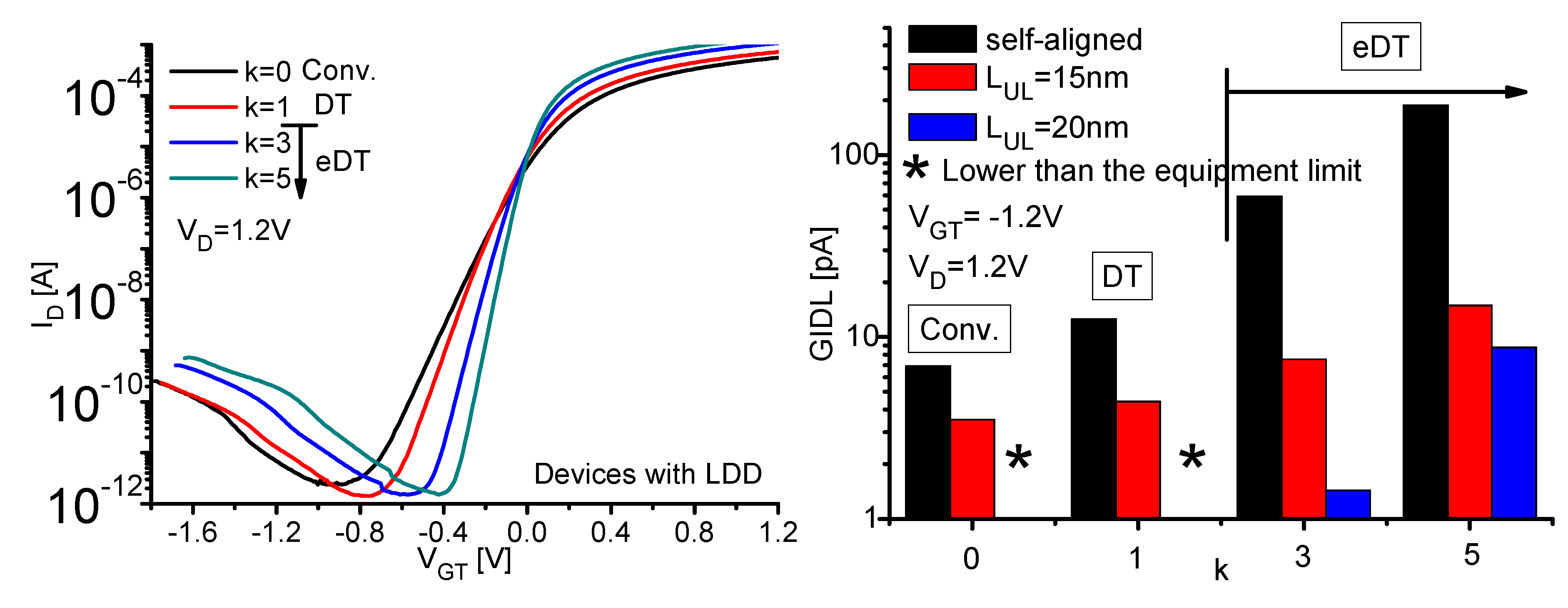
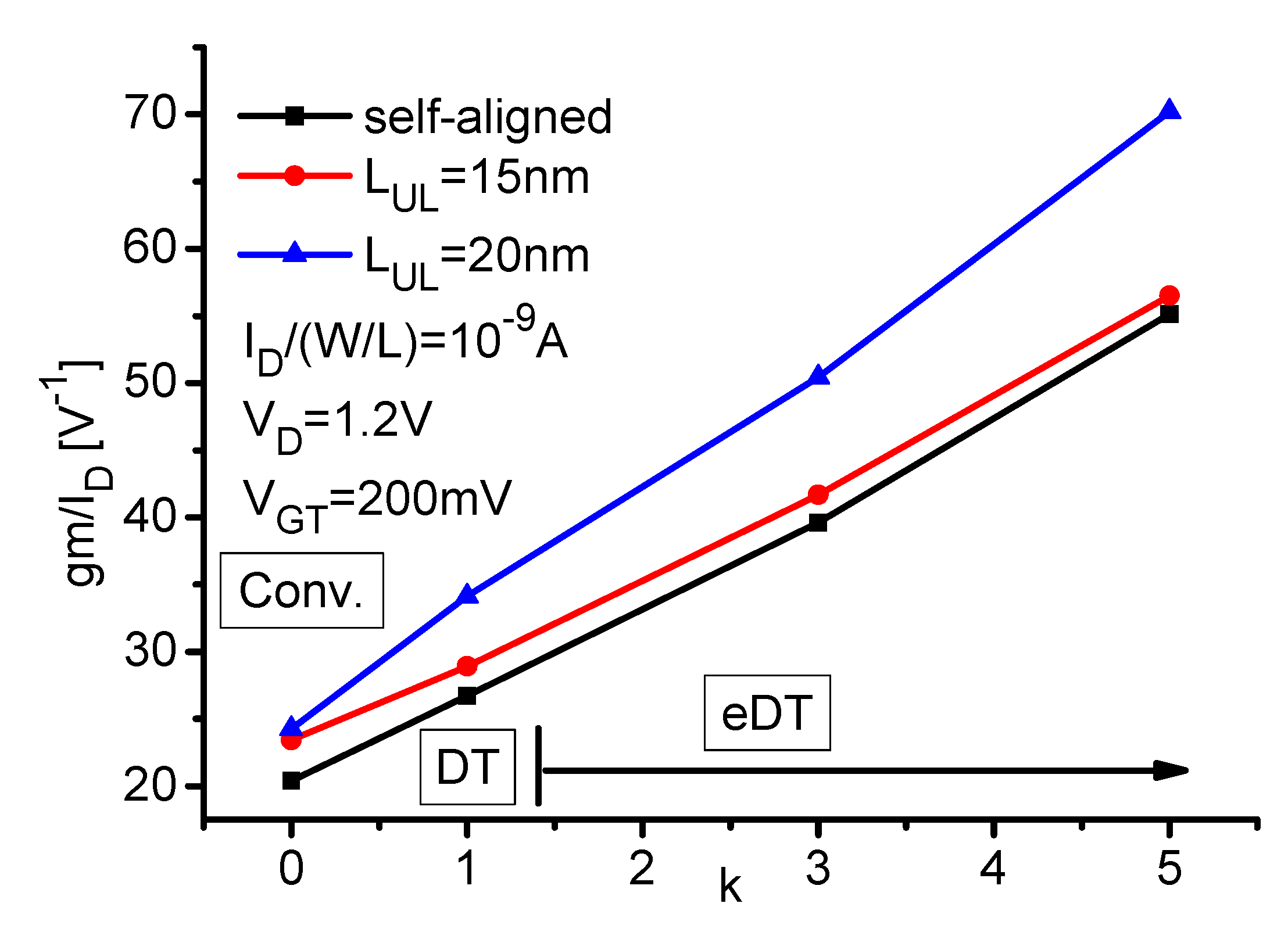
3. Results and Discussion


| Self-Aligned, k = 0 | Self-Aligned, k = 3 | LUL = 20 nm, k = 0 | LUL = 20 nm, k = 3 |
|---|---|---|---|
| 3.08 × 10⁴ | 6.54 × 10⁴ | 6.48 × 10⁴ | 10.52 × 10⁴ |


| k | Threshold Voltage [V] | ||
|---|---|---|---|
| Self-Aligned | LUL = 15 nm | LUL = 20 nm | |
| 0 | 0.45 | 0.48 | 0.48 |
| 1 | 0.40 | 0.40 | 0.37 |
| 3 | 0.29 | 0.30 | 0.25 |
| 5 | 0.22 | 0.24 | 0.20 |


4. Conclusions
Acknowledgments
Author Contributions
Conflicts of Interest
References
- Fenouillet-Beranger, C.; Denorme, S.; Perreau, P.; Buj, C.; Faynot, O.; Andrieu, F.; Tosti, L.; Barnola, S.; Salvetat, T.; Garros, X.; et al. FDSOI devices with thin BOX and ground plane integration for 32 nm node and below. Solid State Electron. 2009, 53, 730–734. [Google Scholar] [CrossRef]
- Fujiwara, M.; Morooka, T.; Yasutake, N.; Ohuchi, K.; Aoki, N.; Tanimoto, H.; Kondo, M.; Miyano, K.; Inaba, S.; Ishimaru, K.; et al. Impact of BOX scaling on 30 nm gate length FD SOI MOSFET. In Proceedings of the 2005 IEEE International SOI Conference, Honolulu, HI, USA, 3–6 October 2005; pp. 180–182.
- Kilchytska, V.; Flandre, D.; Andrieu, F. On The UTBB SOI MOSFET performance improvement in Quasi-Double-Gate Regime. In Proceedings of the ESSDERC—European Solid-State Device Conference, Bordeaux, France, 17–21 September 2012; p. 246.
- Nguyen, B.-Y.; Maleville, C. Advanced Substrate News. 2014. Available online: http//www.advancedsubstratenews.com/2014/03/fd-soi-back-to-basics-for-best-cost-energy-efficiency-and-performance (accessed on 7 May 2014).
- Yan, R.; Duane, R.; Razavi, P.; Afzalian, A.; Ferain, I.; Lee, C.W.; Dehdashti-Akhavan, N.; Bourdelle, K.; Nguyen, B.Y.; Colinge, J.P. LDD Depletion Effects in thin-BOX FDSOI Devices with a Ground Plane. In Proceedings of the IEEE International SOI Conference, Foster City, CA, USA, 5–8 October 2009.
- Nakamura, S.; Kawasaki, J.; Kumagai, Y.; Usami, K. Measurements of the Minimum Energy Point in Silicon-on-Thin-BOX (SOTB) and Bulk MOSFET. In Proceedings of the Joint International EUROSOI Workshop and International Conference on Ultimate Integration on Silicon, Bologna, Italy, 26–28 January 2015; pp. 193–196.
- Ohtou, T.; Saraya, T.; Hiramoto, T. Variable-body-factor SOI MOSFET with ultrathin buried oxide for adaptive threshold voltage and leakage control. IEEE Trans. Electron. Devices 2008, 55, 40–47. [Google Scholar] [CrossRef]
- Yanagi, S.; Nakakubo, A.; Omura, Y. Proposal of partial-ground-plane (PGP) silicon-on-insulator (SOI) MOSFET for deep sub-0.1 μm channel regime. IEEE Electron. Device Lett. 2001, 22, 278–280. [Google Scholar] [CrossRef]
- Xiong, W.; Colinge, J.P. Self-aligned ground-plane fully depleted SOI MOSFET. Electron. Lett. 1999, 35, 2059–2060. [Google Scholar] [CrossRef]
- Kimura, S. Overview of ultra-low power devices, focus on SOTB. In Proceedings of the IEEE SOI-3D-Subthreshold Microelectronics Technology Unified Conference (S3S), San Francisco, CA, USA, 6–9 October 2014.
- Trivedi, V.; Fossum, J.G.; Chowdhury, M.M. Nanoscale FinFETs with Gate-Source/Drain Underlap. IEEE Trans. Electron. Devices 2005, 52, 56–62. [Google Scholar] [CrossRef]
- Santos, S.; Nicoletti, T.; Martino, J.A. Analog Performance of Gate-Source/Drain. Underlap Triple Gate SOI nMOSFET. ECS Trans. 2011, 39, 239–246. [Google Scholar]
- Song, K.-W.; Jeong, H.; Lee, J.-W.; Hong, S.I.; Tak, N.-K.; Kim, Y.-T.; Choi, Y.L.; Joo, H.S.; Kim, S.H.; Song, H.J.; et al. 55 nm Capacitorless. 1T-DRAM Cell. Transistor with non-overlap structure. In Proceedings of the IEEE International Electron Devices Meeting, San Francisco, CA, USA, 15–17 December 2008; pp. 1–4.
- Nicoletti, T.; Santos, S.; Almeida, L.; Martino, J.; Aoulaiche, M.; Veloso, A.; Jurczak, M.; Simoen, E.; Claeys, C. The Impact of Gate Length Scaling on UTBOX FDSOI Devices: The Digital/Analog Performance of Extension-less Structures. In Proceedings of the 13th Ultimate Integration on Silicon, Grenoble, France, 6–7 March 2012; p. 161.
- Fossum, J.G.; Chowdhury, M.M.; Trivedi, V.P.; King, T.-J.; Choi, Y.-K.; An, J.; Yu, B. Physical Insights on Design and Modeling of Nanoscale FinFETs. In Proceedings of the IEEE International Electron Devices Meeting, Washington, DC, USA, 8–10 December 2003.
- Vitale, S.A.; Peter, W.W.; Checka, N.; Kedzierski, J.; Keast, C.L. FDSOI Process Technology Subthreshold Operation Ultra-Low-Power Electronics. In Proceedings of the 219th ECS Meeting, Montreal, QC, Canada, 1–6 May 2011; pp. 179–188.
- Colinge, J.P. An SOI voltage-controlled bipolar-MOS device. IEEE Trans. Electron. Devices 1987, 34, 845–849. [Google Scholar] [CrossRef]
- Sasaki, K.R.A.; Manini, M.B.; Martino, J.A.; Aoulaiche, M.; Simoen, E.; Witters, L.; Claeys, C. Ground plane influence on enhanced dynamic threshold UTBB SOI nMOSFETs. In Proceedings of 9th ICCDCS Conference, Playa del Carmen, Mexico, 2–4 April 2014; pp. 1–4.
- Sasaki, K.R.A.; Manini, M.B.; Simoen, E.; Claeys, C.; Martino, J.A. Enhanced dynamic threshold voltage UTBB SOI nMOSFETs. Solid-State Electron. 2015, in press. [Google Scholar]
- Sasaki, K.R.A.; Aoulaiche, M.; Simoen, E.; Claeys, C.; Martino, J.A. Silicon Film Thickness Influence on Enhanced Dynamic Threshold UTBB SOI nMOSFETs. In Proceedings of the SBMicro 2014, 29th Symposium on Microelectronics Technology and Devices, Aracaju, SE, Brazil, 1–5 September 2014; pp. 1–4.
- Kilchytska, V.; Bol, D.; de Vos, J.; Andrieu, F.; Flandre, D. Quasi-double gate regime to boost UTBB SOI MOSFET performance in analog and sleep transistors applications. Solid State Electron. 2013, 84, 28–37. [Google Scholar] [CrossRef]
- Bol, D.; Kilchytska, V.; de Vos, J.; Andrieu, F.; Flandre, D. Quasi-Double Gate Mode for Sleep transistors in UTBB FD SOI Low-Power High Speed Applications. SOI Conference (SOI). In Proceedings of the 2012 International, Napa, CA, USA, 1–4 October 2012; pp. 1–2.
- Arshad, M.K.M.; Kilchytska, V.; Makovejev, S.; Olsen, S.; Andrieu, F.; Raskin, J.P.; Flandre, D. UTBB SOI MOSFETs Analog Figures of Merits: Effect of Ground Plane and Asymmetric Double Gate Regime. In Proceedings of the EUROSOI, Montpellier, France, 23–25 January 2012; pp. 111–112.
- Le Coz, J.; Pelloux-Prayer, B.; Giraud, B.; Giner, F.; Flatresse, P. DTMOS Power Switch in 28 nm UTBB FD-SOI Technology. In Proceedings of the IEEE SOI-3D-Subthreshold Microelectronics Technology Unified Conference (S3S), Monterey, CA, USA, 7–10 October 2013; pp. 1–2.
- Nicoletti, T.; Santos, S.D.; Sasaki, K.R.A.; Martino, J.A.; Aoulaiche, M.; Simoen, S.; Claeys, C. The Activation Energy Dependence on the Electric Field in UTBOX SOI FBRAM Devices. In Proceedings of the IEEE SOI-3D-Subthreshold Microelectronics Technology Unified Conference (S3S), Monterey, CA, USA, 7–10 October 2013; pp. 1–2.
- Santos, S.D.; Nicoletti, T.; Aoulaiche, M.; Martino, J.A.; Veloso, A.; Jurczak, M.; Simoen, E.; Claeys, C. In ECS Transactions, Spacer Length and Tilt Implantation Influence on Scaled UTBOX FD MOSFETs. In Proceedings of the SBMicro 2012: 27th Symposium on Microelectronics Technology and Devices, 30 August–2 September 2012; pp. 483–489.
- Sasaki, K.R.A.; Aoulaiche, M.; Simoen, E.; Claeys, C.; Martino, J.A. Influence of Underlap on UTBB SOI MOSFETs in Dynamic Threshold Mode. In Proceedings of the IEEE SOI-3D-Subthreshold Microelectronics Technology Unified Conference (S3S), San Francisco, CA, USA, 6–9 October 2014; pp. 1–3.
- Woo, J. Tunnel-FETs. In Proceedings of IEEE SOI-3D-Subthreshold Microelectronics Technology Unified Conference (S3S), San Francisco, CA, USA, 6–9 October 2014.
- Sasaki, K.R.A.; Nicoletti, T.; Almeida, L.; Santos, S.D.; Nissimoff, A.; Aoulaiche, M.; Simoen, E.; Claeys, C.; Martino, J.A. Improved retention times in UTBOX nMOSFETs for 1T-DRAM applications. Solid State Electron. 2014, 97, 30–37. [Google Scholar] [CrossRef]
© 2015 by the authors; licensee MDPI, Basel, Switzerland. This article is an open access article distributed under the terms and conditions of the Creative Commons Attribution license (http://creativecommons.org/licenses/by/4.0/).
Share and Cite
Sasaki, K.R.A.; Aoulaiche, M.; Simoen, E.; Claeys, C.; Martino, J.A. Extensionless UTBB FDSOI Devices in Enhanced Dynamic Threshold Mode under Low Power Point of View. J. Low Power Electron. Appl. 2015, 5, 69-80. https://doi.org/10.3390/jlpea5020069
Sasaki KRA, Aoulaiche M, Simoen E, Claeys C, Martino JA. Extensionless UTBB FDSOI Devices in Enhanced Dynamic Threshold Mode under Low Power Point of View. Journal of Low Power Electronics and Applications. 2015; 5(2):69-80. https://doi.org/10.3390/jlpea5020069
Chicago/Turabian StyleSasaki, Katia Regina Akemi, Marc Aoulaiche, Eddy Simoen, Cor Claeys, and Joao Antonio Martino. 2015. "Extensionless UTBB FDSOI Devices in Enhanced Dynamic Threshold Mode under Low Power Point of View" Journal of Low Power Electronics and Applications 5, no. 2: 69-80. https://doi.org/10.3390/jlpea5020069
APA StyleSasaki, K. R. A., Aoulaiche, M., Simoen, E., Claeys, C., & Martino, J. A. (2015). Extensionless UTBB FDSOI Devices in Enhanced Dynamic Threshold Mode under Low Power Point of View. Journal of Low Power Electronics and Applications, 5(2), 69-80. https://doi.org/10.3390/jlpea5020069