Article

Multiple Bit Error Tolerant Galois Field Architectures Over GF (2m)

by
Mahesh Poolakkaparambil
1,*,
Jimson Mathew
2 and
Abusaleh Jabir
1
1
Oxford Brookes University, SOT, Wheatley Campus, OX33 1HX Oxford, UK
2
Department of Computer Science, University of Bristol, Merchant Venturers Building, Woodland Road, BS8 1UB Bristol, UK
*
Author to whom correspondence should be addressed.
Electronics 2012, 1(1), 3-22; https://doi.org/10.3390/electronics1010003
Submission received: 14 May 2012 / Revised: 29 May 2012 / Accepted: 11 June 2012 / Published: 26 June 2012
(This article belongs to the Special Issue Feature Papers)

Abstract

:
Radiation induced transient faults like single event upsets (SEU) and multiple event upsets (MEU) in memories are well researched. As a result of the technology scaling, it is observed that the logic blocks are also vulnerable to malfunctioning when they are deployed in radiation prone environment. However, the current literature is lacking efforts to mitigate such issues in the digital logic circuits when exposed to natural radiation prone environment or when they are subjected to malicious attacks by an eavesdropper using highly energized particles. This may lead to catastrophe in critical applications such as widely used cryptographic hardware. In this paper, novel dynamic error correction architectures, based on the BCH codes, is proposed for correcting multiple errors which makes the circuits robust against radiation induced faults irrespective of the location of the errors. As a benchmark test case, the finite field multiplier circuit is considered as the functional block which can be the target for major attacks. The proposed scheme has the capability to handle stuck-at faults that are also a major cause of failure affecting the overall yield of a nano-CMOS integrated chip. The experimental results show that the proposed dynamic error detection and correction architecture results in 50% reduction in critical path delay by dynamically bypassing the error correction logic when no error is present. The area overhead for the larger multiplier is within 150% which is 33% lower than the TMR and comparable to 130% overhead of single error correcting Hamming and LDPC based techniques.

1. Introduction

Malfunctioning of the integrated circuits (ICs) under radiation effects is mostly reported when the circuits are deployed in space related applications where the operating conditions are very often interfered by high intensity and high energy radiation particles. Recently, it is also noted that the desired operations of such ICs when fabricated over silicon are also disrupted in ground based operations [1,2]. In the past, faulty operations of chips due to interference of radiation particles from the packaging materials are reported by major semiconductor industries [2]. Since then significant research has been undertaken towards analyzing the impact of radiation on semiconductor based ICs. The data processed within ICs can be analyzed and decoded using the controlled radiation attack on the semiconductor devices. This has lead to threat against cryptographic hardware circuits whose primary goal is to secure the data that it processes [3,4,5].
The cryptographic processors dictate almost every aspect of our lives, such as bank transactions, digital rights management, TV set-top boxes, smart cards, and mobile communications [6]. It has been reported that electronic hardware dedicated to such critical applications when subjected to radiation critical environment, either by natural causes or induced by a hardware hacker for the purpose of IP theft, may exhibit faults with catastrophic consequences. This is in addition to other causes, e.g., manufacturing defects, etc., for a hardware to become faulty. The primary arithmetic block in most of the cryptographic processors is a finite field multiplier [7,8]. Hence these circuits can be subjected to tampering for leaking out information during a critical operation. During its normal operation when high energy particle comes in contact with nano-scale logic devices, it can cause upsets in the actual computational results of these devices. A malicious attacker hence can also subject the cryptographic chip to controlled radiations in a laboratory environment so as to make the integrated chip perform faulty. The advantage of this is that, the attacker is not permanently tampering or damaging the chip but only making it perform faulty in the presence of radiation event [9]. Thus one can leak out the required information such as IP, secret data and other side information without tampering the chip physically.
The remainder of this paper is organized as follows. Section 2 explains the prior research in the related area. Section 3 presents the fundamentals of Galois field arithmetic in order to help the readers to quickly follow the basics. Section 4 presents the novel multiple error correction architecture based on the BCH code for designing a radiation hardened digital circuit. Section 5 presents a novel and improved design architecture for the critical path delay reduction. ASIC prototyping and experimental results are explained in Section 6. The conclusions and the future extensions are presented in Section 7.

2. Prior Research

As the integration density in modern ICs increases with technology scaling, the supply voltage required to charge and discharge the capacitors is reducing rapidly. Hence it is becoming easier to disrupt the nano-scale devices operating at lower voltages with external interference. When a high intensity radiation imparts on the silicon surface where the miniature nano-scale devices are present, the high energy particles, such as alpha and gamma particles, lose their energy and create an ionized region over the area of impact. This ionization produces transient current pulses that eventually affects the data processed by the nano-scale devices. Such transient current pulses can cause a bit flip in a critical node of the functional logic that can propagate to multiple nodes. This leaves the device temporarily faulty [1]. This kind of temporary fault is known as a transient error.
Several techniques are presented in literature to mitigate such transient errors. One such approach is based on space redundancy, where the functional block is replicated multiple times and the correctness is checked with the help of a voter. One example for such a space redundant scheme is the Triple Modular Redundancy (TMR). In TMR, the actual functional block is replicated three times and the output is compared for correctness with a voter [10]. If two out of three modules agree to a result to be correct, the voter considers that as the final result of the circuit. The major drawback of TMR is that, the hardware overhead is always more than 200%. Another issue of TMR is that the reliability depends on the voter and also the assumption is that the error occurs only in one functional block out of three. Another approach for error detection is based on time redundancy, e.g., the Concurrent Error Detection (CED) [11,12]. In CED, an additional error monitoring block is included with the actual circuit that flags the occurrence of an error. Once the error flag is active, the functional block rolls back and recomputes. This induces a high delay penalty to the calculation that may be unsuitable for many applications.
Several approaches are reported for double error detection and single error correction commonly known as the SEC/DED schemes. The SEC/DED schemes are based on hamming or LDPC codes that can correct only single bit errors in the calculations [13,14]. But analysis shows that a transient error occurring at one critical node can cause multiple output errors due to multiple fan-outs of the circuits. Other known but least explored approaches are based on inherent properties of the functional blocks. One such method is based on implication based error detection. Implication exist in any circuits and their violation can be used to detect error occurrence [2].
It is evident from the above discussions that a viable scheme for handling multiple error detection and correction resulting form radiation induced transient errors is not yet fully explored. This paper presents two novel transient error correcting techniques based on BCH codes that can correct burst errors. Our proposed architecture is designed to address the high area overhead of TMR, the time redundancy of CED and roll back, and to enable multiple error correction, which is missing in most of the existing single error correcting designs. Also unlike the techniques of [3,13], which consider errors that occur only within the functional block, our scheme considers the errors both in the functional block as well as the redundant bit generation block. In this regard, our first method can correct multiple transient errors anywhere within the design with a penalty of only an extra decoder delay. In the second method, this has been further improved with novel bypass circuitry, which is capable of saving the critical path delays by up to 50%.

3. Preliminaries of Galois Field (GF) Arithmetic

For every prime number p, there exists a Galois field, also known as the finite field, over the set GF(p) having p elements with special elements 0 and 1 as the additive and multiplicative identities, respectively. It is possible to extend the fields over GF(p) to a field that consists of pm elements, where m is a nonzero positive integer. This extended field over the set GF(pm) is known as the extension of the field over GF(p). Let “+” and “·” represent the addition and multiplication operations on the field elements. Then GF(pm) forms a finite field if it forms a commutative ring with identity over these two operations. The finite fields over GF(2) and their extensions over GF(2m) are used in digital logic owing to the field elements 0 and 1 only as well as their carry free logic and ease of implementation in hardware.
The finite fields over GF(2m) can be generated with monic irreducible polynomials of the form: P ( x ) = x m + i = 0 m 1 c i . x i , where ci ∈ GF(2) [15]. Other than elements 0 and 1 the field consists of primitive elements that are multiples of the element α, where α is the root of P(x) i.e., P(α) = 0, and P(x) is the primitive polynomial of the field. To ensure that the operations over the fields are finite, any element in the field having power > (m − 1) is reduced to an element with power < (m − 1) by reducing it with P(x). The set of elements {0, 1, α, α2, …, αm−1} forms elements of the polynomial basis (PB) over a certain primitive polynomial. Any element A ∈ GF(2m) is represented using the elements in PB. The polynomial basis multiplication of A(x) and B(x) over GF(2m) is defined using the following expression: C(x) = A(x) · B(x) mod P(x) where A, B ∈ GF(2m) [15].
Many architectures exists in literature for finite field multiplication such as bit-serial, bit- parallel, digit serial and systolic architectures [16,17]. To simplify the finite field multiplication, an algorithm and equivalent hardware implementation is presented in [18]. This scheme is further modified and a reduced complexity bit parallel PB multiplier is introduced in [19] . In this paper, the multiplier structure is adopted from [19].

4. The Proposed Methodology for Multiple Bit Error Correction

As evident from the above discussions, there is no scheme in the current literature that can correct more than two random output bit errors including those in the correction block. This section explains the BCH error correction scheme to mitigate radiation induced temporal errors in detail along with its efficient hardware implementation. To the best of our knowledge, the technique presented in this paper is first to investigate such a scheme for fault tolerant Galois field circuits. However the scope of the proposed technique here is to focus on the error that are happening on the internal nodes of the circuit. Hence we assume that the primary input is error free.

4.1. Bose–Choudhury–Hocquenghem Code

The Bose–Choudhury–Hocquenghem (BCH) codes belong to the family of cyclic codes in which the message block is encoded using a polynomial g(x), called the generator polynomial. The generator polynomial is the least common multiplier (LCM) of the minimal polynomial for the selected powers with respect to GF(2m), provided that each of the minimal polynomial should appear only once in the product. Here, the message is treated as a whole block and encoded one at a time rather than encoding continuously as in the case of convolution codes. The encoder block possesses no memory, hence no information of the previous message blocks. This style of encoding can be thought of as sliding an encoding window over the message bits. In the conventional BCH codes, the LFSR structure is used to encode incoming message bits one at a time. Hence, the present encoded bit depends on the previous bit, which shows that a memory is being used. In the proposed scheme, a parallel implementation of the BCH encoder is introduced which encodes the message as a whole block and uses no memory. The binary BCH codes are generalized Hamming codes. The BCH codes detect and correct randomly located bit errors in a stream of information bits according to its error correction capability (t). The burst error correcting codes, such as the Reed–Solomon codes, correct multiple errors within a symbol or multiple symbols, but all the bit errors must be within the same symbol. The most interesting aspect of the BCH codes over Reed–Solomon codes for our purpose is the simplicity in decoding the codewords. In this case, the bit’s location only needs to be determined and not the correct value, as in the case of Reed–Solomon codes. The basic block diagram of the generic multiple bit error correction circuit using the binary BCH code is shown in 
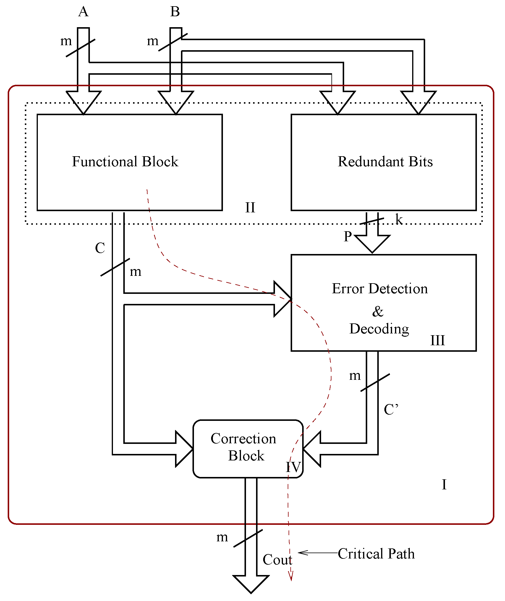
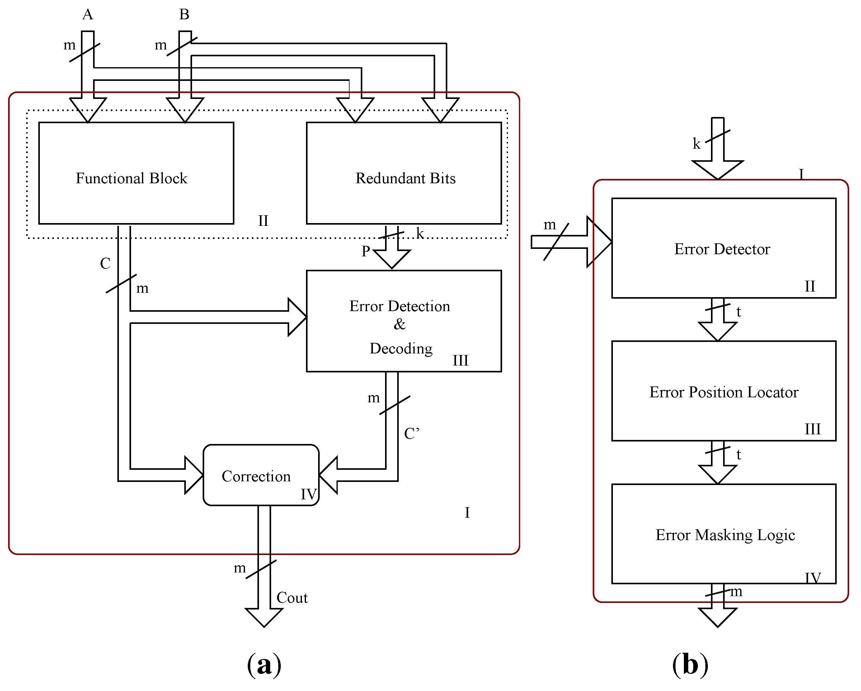
Figure 1(a). The overall design contains a redundant bit generation block that works in parallel with the functional block, an error detection and decoding block that detects the occurrence of an error and its location, and finally a decoder, apart from the bit parallel multiplier functional block.
Figure 1. BCH code based multiple detection and correction architectures. (a) Multiple error correction architecture; (b) Error detection and correction block.
Electronics 01 00003 g001

4.2. BCH Encoder and Decoder Design

The complete design of a BCH parallel encoder and decoder with an example is now discussed. The bit parallel multiplier architecture is adopted from [19]. The general representation of BCH code is BCH(n, k, d), where n is the size of the codeword or, in other words, it is the sum of the message length k, and the number of parity bits p used for encoding, and d is the minimum distance (dmin) between the codewords. The possible BCH codes for m ≥ 3 and t < 2m−1 is given by the following expressions:
Block   length : n = 2 m 1
Number   of   check   bits : n k m t
Minimum   distance: : d min 2 t + 1
The codeword is formed by adding the remainder after dividing the shifted message block by a generator polynomial g(x). All the codewords are multiples of the generator polynomial. The generator polynomial is not just a minimal primitive polynomial, but a combination of several polynomials corresponding to the powers of the primitive element α in GF(2m). In other words, g(x) is the least common multiple of the minimal polynomials over the various powers of the primitive element α (powers from α, α2, …, α2t, where t is the error correction capability of the code). Then,
g ( x ) = LCM m 1 ( x ) , m 2 ( x ) , , m 2 t ( x )
where m1(x), m2(x), … m2t(x) are the minimal polynomials corresponding to the various powers of α. It is also noted that every even power of a primitive element has the same minimal polynomial. Hence Equation (4) is simplified to the following:
g ( x ) = LCM m 1 ( x ) , m 3 ( x ) , , m 2 t 1 ( x ) .
The basic principle and design of the bit-parallel BCH code based multiple error correction scheme is explained with an example as follows. Let us consider a simple case of BCH(15, 5, 7), where n = 15 and k = 5. In this fairly small example, we consider bit-parallel PB multiplier over GF(25). Let c = [co, c1, c2, c3, c4] be the outputs of the multiplier. Then,
M ( x ) = c 4 x 4 + c 3 x 3 + c 2 x 2 + c 1 x + c 0
x n k M ( x ) = x n k ( c 4 x 4 + c 3 x 3 + c 2 x 2 + c 1 x + c 0 ) = c 4 x 14 + c 3 x 13 + c 2 x 12 + c 1 x 11 + c 0 x 10
as in this case n = 15 and k = 5.
The redundant bits are generated by the following:
P ( x ) = x n k M ( x ) mod g ( x ) .
Let α be the primitive element of GF(24). Here, P(x) = x4 + x + 1 is the primitive polynomial. The three minimal polynomials m1(x), m3(x), and m5(x) are given by:
m 1 ( x ) = x 4 + x + 1 ,
m 3 ( x ) = x 4 + x 3 + x 2 + x + 1 ,
m 5 ( x ) = x 2 + x + 1 .
For three bit error correction (t = 3), the generator polynomial for constructing the codeword is then given by the following:
g ( x ) = L C M ( m 1 ( x ) , m 3 ( x ) , m 5 ( x ) ) .
Substituting the minimal polynomials, the following expression is obtained:
g ( x ) = x 10 + x 8 + x 5 + x 4 + x 2 + x + 1
Substituting the generating polynomial, the following expression is obtained:
P ( x ) = p 9 x 9 + p 8 x 8 + p 7 x 7 + p 6 x 6 + p 5 x 5 + p 4 x 4 + p 3 x 3 + p 2 x 2 + p 1 x 1 + p 0
where, p0 = c0 + c2 + c4, p0 = d0 + d2 + d4 + e0 + e1 + e2 + e3, p1 = c0 + c1 + c2 + c3 + c4 p1 = d0 + d1 + d2 + d3 + d4, p2 = c0 + c1 + c3, p2 = d0 + d1 + d3 + e1 + e2 + e3, p3 = c1 + c2 + c4, p3 = d1 + d2 + d4 + e0 + e2 + e3, p4 = c0 + c3 + c4, p4 = d0 + d3 + d4 + e0 + e2, p5 = c0 + c1 + c2, p5 = d0 + d1 + d2 + e2, p6 = c1 + c2 + c3, p6 = d1 + d2 + d3 + e0 + e3, p7 = c2 + c3 + c4, p7 = d2 + d3 + d4 + e1, p8 = c0 + c2 + c3, p8 = d0 + d2 + d3 + e0 + e1 + e3, p9 = c1 + c3 + c4, p9 = d0 + d3 + d4 + e0 + e2, where the d and e terms are the inner product terms of the multiplier [19]. Hence, the final BCH encoded codeword for the bit parallel GF multiplier circuit is given as the following expression:
E ( x ) = c 4 x 14 + c 3 x 13 + c 2 x 12 + c 1 x 11 + c 0 x 10 + p 9 x 9 + p 8 x 8 + p 7 x 7 + p 6 x 6 + p 5 x 5 + p 4 x 4 + p 3 x 3 + p 2 x 2 + p 1 x + p 0 .
The redundant bits (check bits) are generated by a parallel redundant bit generation unit as shown in Figure 1(a). The resulting parity bits along with the multiplier outputs are passed on to the error detection and correction block (syndrome generation and decoding) as shown in Figure 1(b). For three bit error correction capability (t = 3), six (2 × t) syndromes need to be generated. The syndromes help us to determine whether the computed multiplication results are error free or not. In case of error free computation, the syndromes will be evaluate to zero. If the syndromes are nonzero, then that flags us the erroneous computation. The syndromes are calculated using the following expression:
S i ( x ) = E ( x ) | x = 1 , α , , α 2 t .
The syndrome decoding is done by using the well known Peterson–Gorenstein–Zierler algorithm. In our work we use only three syndromes to predict and correct errors instead of 6 syndromes in case of classical BCH scheme. This would reduce area of the whole implementation. Here for three bit error correction we need to calculate only syndromes S1, S3, and S5. The generalized equation for syndromes for the given example of BCH(15, 5, 7) are given as follows:
S1 = s13α3 + s12α2 + s11α + s10α, S3 = s33α3 + s32α2 + s31α + s30α, S5 = s53α3 + s52α2 + s51α + s50α, s10 = c4 + c3 + c4 + c0 + p8 + p7 + p4 + p0, s11 = c2 + c1 + c0 + p9 + p7 + p5 + p4 + p1, s12 = c3 + c2 + c1 + c0 + p8 + p6 + p5 + p2, s13 = c4 + c3 + c2 + c1 + p9 + p7 + p6 + p3, s30 = c4 + c0 + p9 + p5 + p4 + p0, s31 = c4 + c3 + p9 + p8 + p4 + p3, s32 = c4 + c2 + p9 + p7 + p4 + p2, s33 = c4 + c3 + c2 + c1 + p9 + p8 + p7 + p6 + p4 + p3 + p2 + p1, s50 = c4 + c2 + c1 + p9 + p8 + p6 + p5 + p3 + p2 + p0, s51 = c4 + c3 + c1 + c0 + p8 + p7 + p5 + p4 + p2 + p1, s52 = c4 + c3 + c1 + c0 + p8 + p7 + p5 + p4 + p2 + p1, s53 = 0.
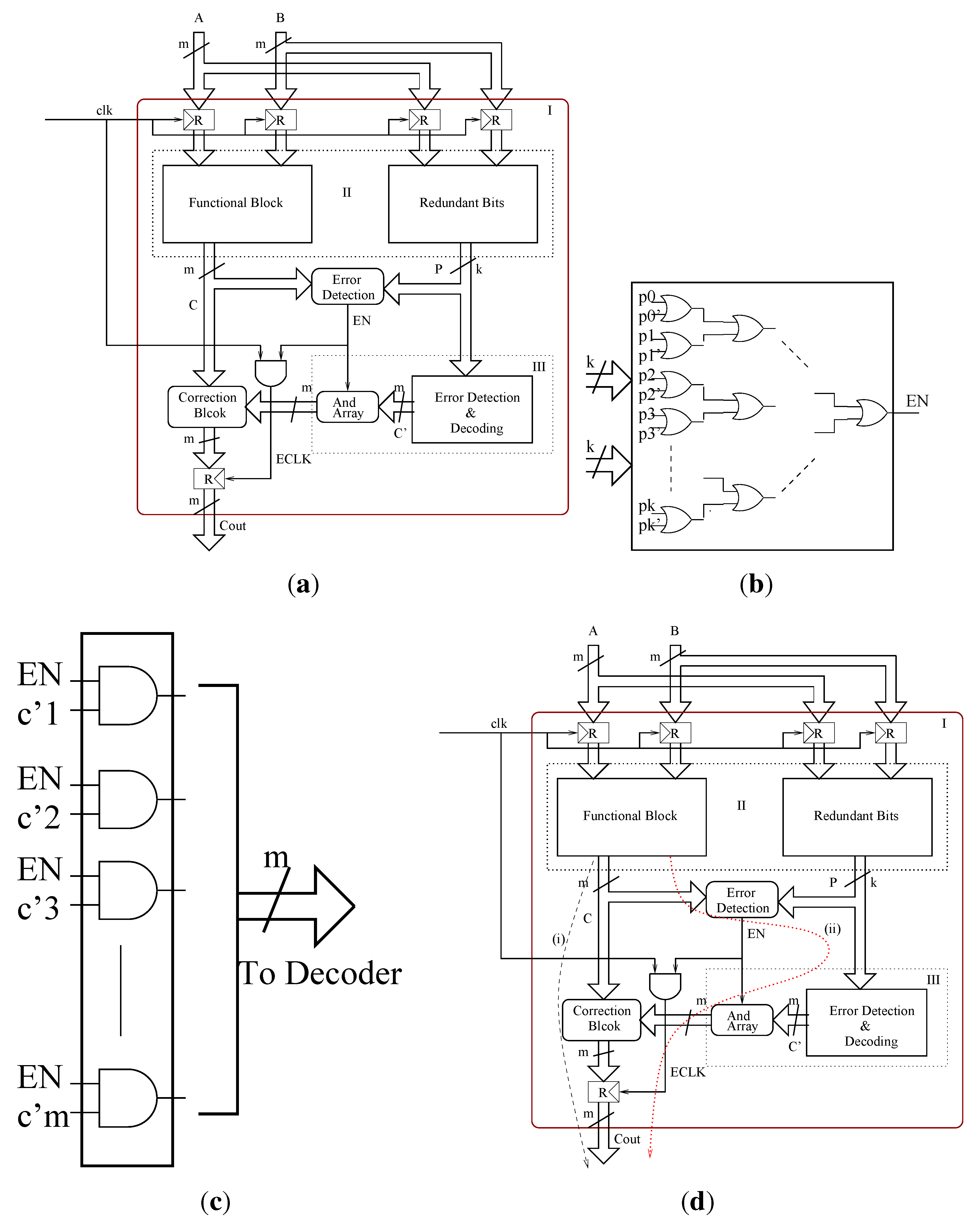
Determining whether the computation is error free is not sufficient; we also need to correct these errors in case if they are present. For this, we need to compute the error positions or error locations of the erroneous bits. To determine the error positions effectively, we need to decode the syndromes. The syndrome decoding block (error detection and correction block) of the BCH based error correction technique contains an error locator polynomial generator block that finds the root of the error locator polynomial and a decoder that eventually corrects the erroneous bits based on the computed error position. For this purpose the computed syndrome values are passed on to the error locator polynomial computation block, as shown in Figure 2. For the three (t = 3) bit error correction, we have three (t = 3) coefficients for the error locator polynomial. Let σ1, σ2, and σ3 be the three coefficients of the error locator polynomial. Then they are calculated as follows:
σ 1 = S 1 ,
σ 2 = ( S 1 2 S 3 ) + S 5 ( S 1 3 + S 3 ) , and
σ 3 = ( S 1 3 + S 3 + S 1 σ 2 ) .

4.3. Improved Error Locator Design

Once we have the error locator polynomial, the roots of the polynomial will give the error locations. The traditional algorithms for finding the roots of the error locator polynomial are based on exhaustive search methods. Another scheme for finding the roots is the Chien search algorithm, in which all the possible values of the primitive element α, ranging from α0, α, … α2m−1, are inserted into the error locator polynomial to check if they satisfy the polynomial. In the proposed design, a bit parallel implementation of the area optimized Chien search algorithm is proposed. In particular, we proposed a scheme in which the root of the error locator polynomial is checked only among the powers of the primitive element α corresponding to the bit positions of the message bits, i.e., the multiplier output bits. The roots of the error locator polynomial corresponding to the parity bits are omitted in order to reduce the hardware complexity and hence the chip area. For a 5-bit multiplier, we check whether α1, α2, α3, α4, α5 are roots of the error locator polynomial, which in turn corresponds to the bit positions c4, c3, c2, c1 and c0 in the output of the multiplier. In other words, if α is a root of the error locator polynomial, it says that the bit c4 of the multiplier is erroneous, etc. The decoder corrects the erroneous bit(s) corresponding to the information provided by the parallel root search block. Based on this design principle, we have also extended the design to a 16-bit parallel PB multiplier over GF(216) and to a 45-bit parallel PB multiplier over GF(245).

4.4. ASIC Prototyping

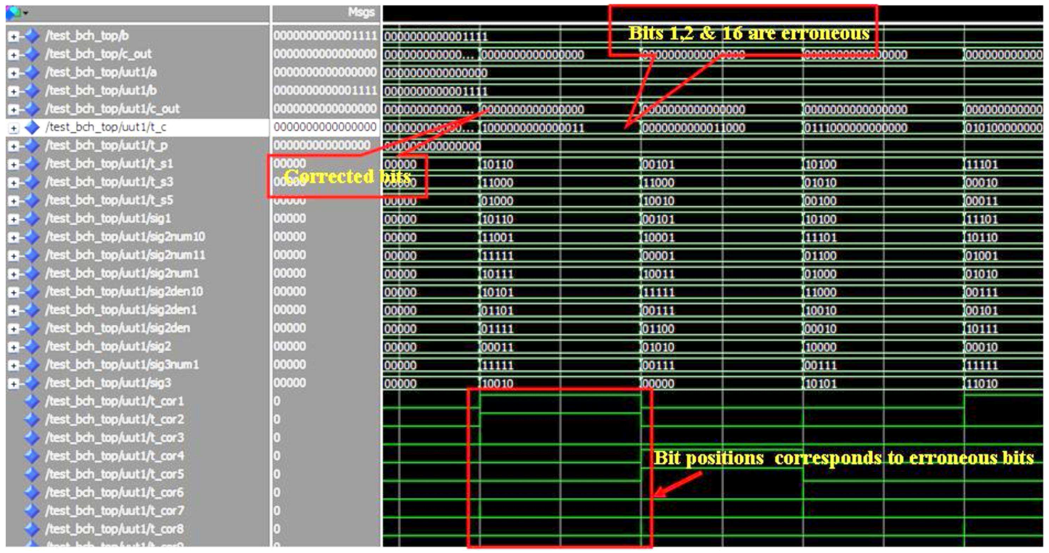
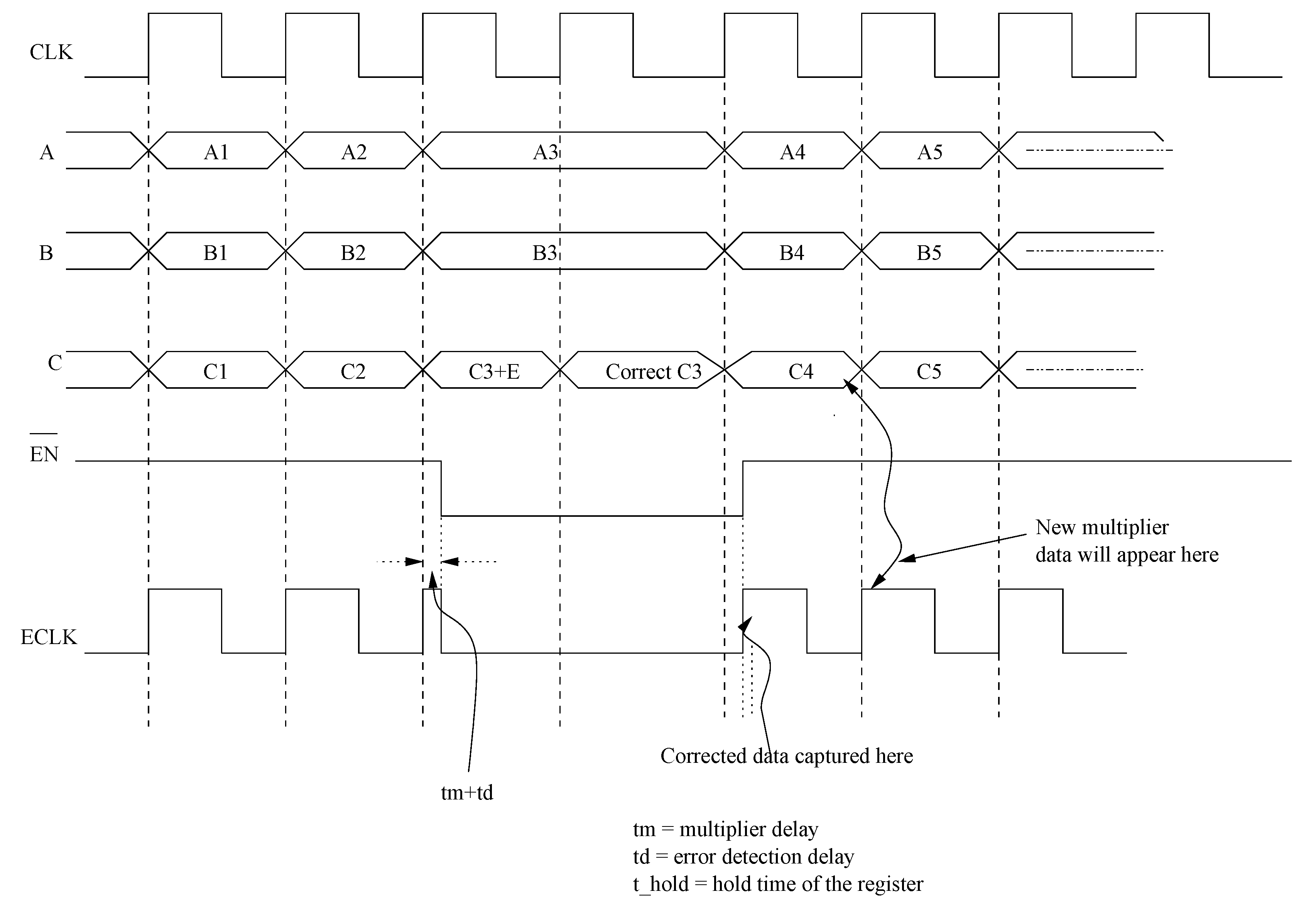
The design was simulated in Modelsim™ . 
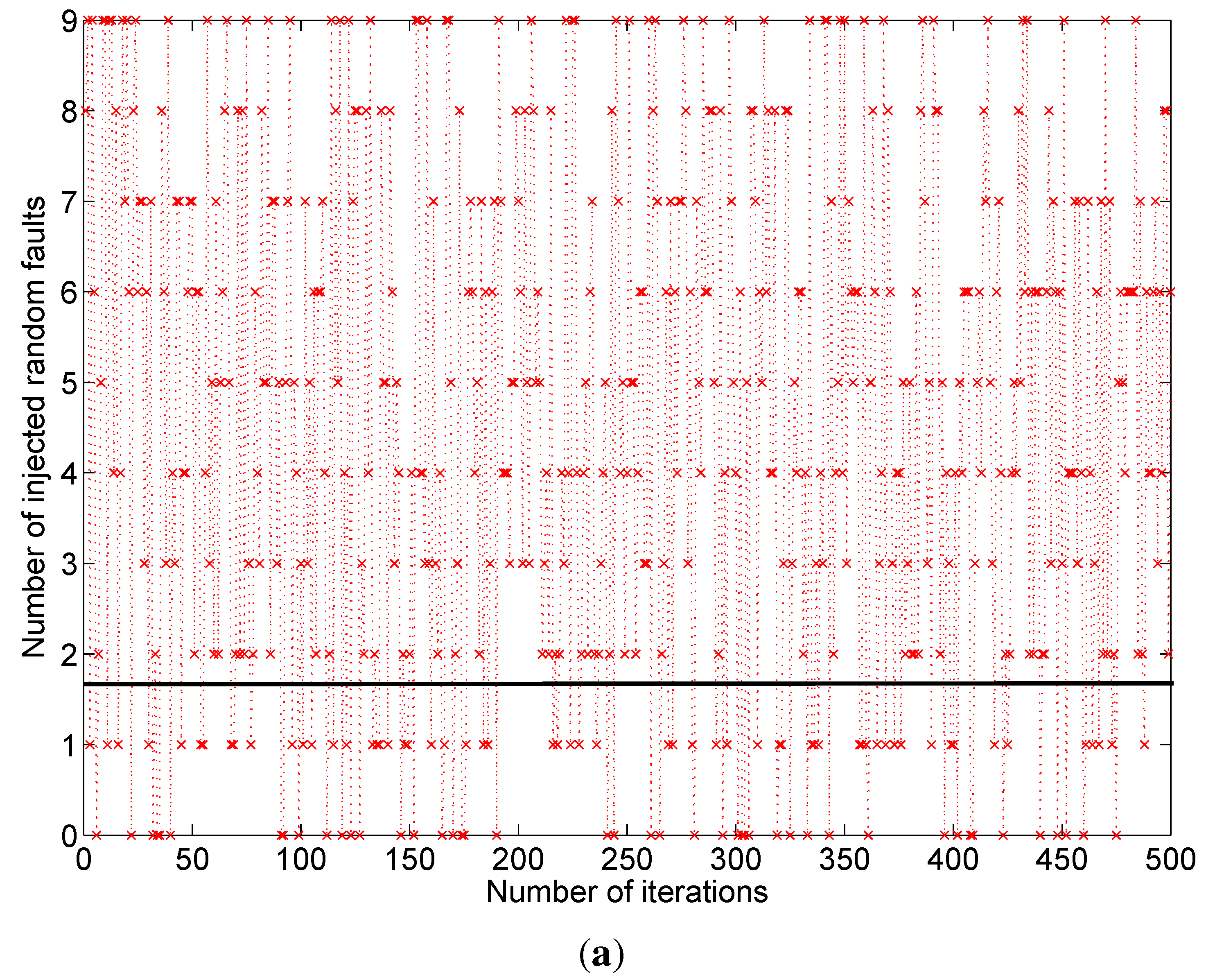
Figure 2 shows the snapshot of a typical Modelsim™ simulation result. During the simulations, the faults are introduced into the multiplier outputs randomly for checking the error correction capability of the proposed scheme. The highlighted parts in Figure 2 show one of the many testing values. The errors are introduced in the intermediate stages of the multiplier, which in turn gave multiple bit errors at the multiplier output. In this case we have errors at bit positions 1, 2, and 16, however the cout values show the corrected final output from the BCH decoder. Although the example designs considered 2 to 5-bit error correction capability, based on the theory presented in this paper, the capability can be extended to more than five bits and also to any digital circuit in general.
Figure 2. Simulation results of BCH code based multiple error correction.
Electronics 01 00003 g002

4.5. Comparison with Existing Approaches

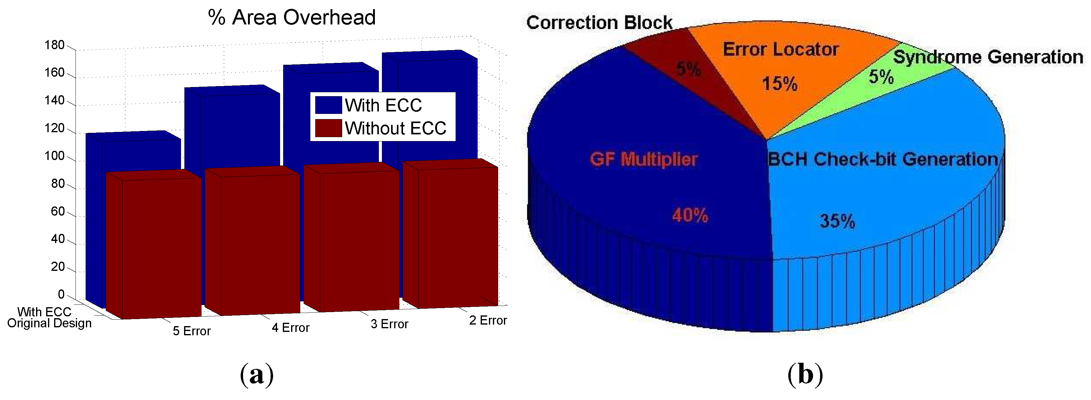
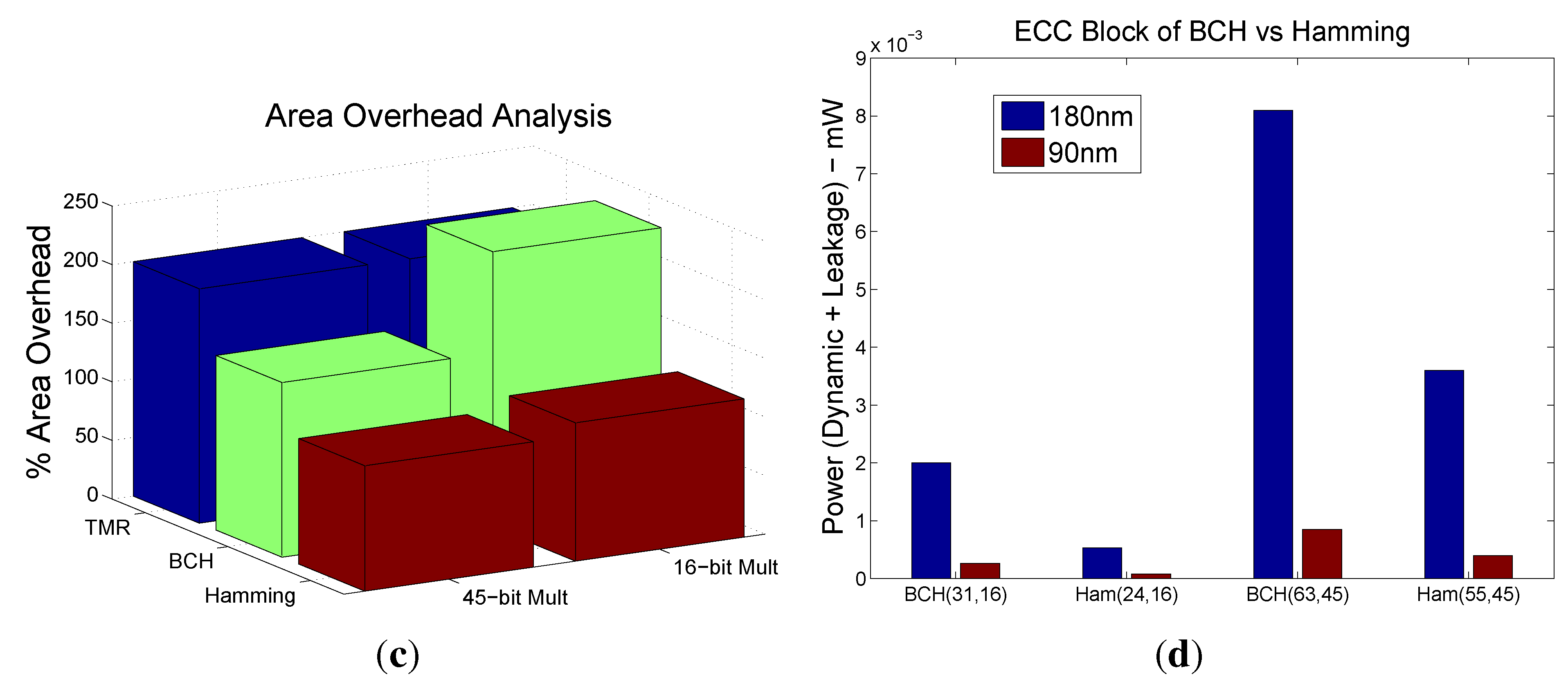
The area overhead for the various designs with 2, 3, 4 and 5 error correction for a 45-bit multiplier is shown in Figure 3(a). It is observed that for a fixed size multiplier, the area increases with the number of bit error correction.
Figure 3. Area overhead analysis for comparative perspective. (a) Overhead analysis of BCH based error correction scheme; (b) Block wise area of a 45-bit GF multiplier with 3-bit error correction.Error LocatrorError Locator
Electronics 01 00003 g003
The area of the various blocks in the proposed multiple error correction scheme is shown in Figure 3(b). The additional area contribution to the over all design is due to the parity predictor block and the Chien search root finding block.
Table 1 compares the area overhead of our approach with other existing related error detection or correction methods appeared in existing literature.
Table 1. Comparison with Other Approaches for 45-bit multiplier.
PropertyTMRMathew et al. 2008 [13]Mathew et al. 2008 [14]ProposedProposedProposed
#errors correctionmultiplesinglesingle3 Errors4 Errors5 Errors
Coding techniqueVotingHammingLDPCBCHBCHBCH
Overhead>200%>130%120%150.4%164.04%170.4%
Further, for a given error correction capability, the extra hardware comes down significantly for larger and more practical designs. For example, for the 5-, 16-, and 45-bit multipliers we observed that the extra hardware is 600%, 240%, and 150.4%, respectively, for 3-bit error correction capability.

5. Extension to Intelligent and Dynamically Error Correctable Architecture

From the above discussions, it is noted that the BCH error correction block runs in parallel with the example finite field multiplier circuit all the time irrespective of the error position or location. In other words, the error correction block in the entire circuitry contributes towards the critical path delay almost all the time, thus affecting the speed of operation, which is a vital factor in most of the present day VLSI systems. Hence immense care has to be taken to reduce this factor as much as possible. In the proposed error correction scheme, we need the error correction block to be active only in case of a fault or error. In this section, we propose a scheme to intelligently activate the ECC block only when there is an error injected or a fault occurred in the circuit on the fly. This scheme is proposed on the premise that the probability of occurrence of an error is very low, e.g., it may happen only once in a million clock cycles. Therefore, we modify the proposed architecture to dynamically (on the fly) correct the errors as they appear. This would free the design from unwanted delay penalty due to the decoder block and make it more efficient. When errors occur, the clock cycle is dynamically extended by a gated clock and the data is captured in the following clock edge instead of the current clock edge where the errors appeared. This novel scheme would give flexibility and time for the ECC block to be active and compute the correct results from the parity information that is computed in parallel with the multiplier and give the correct result in the following clock cycle. It should be noted that, this is unlike CED and rollback, in which once error is detected, other system operations are halted until the recomputation is finished. But in our technique, this problem does not occur as the system runs without stalling.

5.1. The Proposed Extended Architecture

The critical path of the error correcting architecture without the dynamic error correction capability is shown in Figure 4. Clearly, when no error is present in the design during a specific clock cycle, the critical path has added delay of the decoder block. In order to mitigate this issue the architecture in Figure 1(a) has been redesigned as shown in Figure 5(a). In comparison with the architecture in Figure 1(a) our extended design has an extra circuitry (with minor hardware penalty) that check for the occurrence of an error. If there are no errors occurred during a multiplication operation, the output is directly taken from the GF multiplier bypassing the computation result of the error correction block. If there is a bit flip at the multiplier output as a result of faults, the error monitoring circuitry sets a flag bit EN. Once the EN bit is high (indicating the error), the GF multiplier result computed at the current clock cycle will be omitted and an extra clock cycle will be given for correction. The corrected output will be then available in the next clock cycle. This is done using a clocked gate and a AND gate array as shown in Figure 5(a). Depending upon the signal EN, the critical path of the design takes either path i or path ii as shown in Figure 5(d). The critical path is i when EN signal is low (no error) and path ii is taken when EN is high (error occurred). The timing diagram of the proposed extended design is shown in Figure 6. The Signal ECLK follows the CLK as long as there are no errors occurred. Once EN signal goes high that in turn drives ECLK to go low for one clock cycle. This adjustment enables the circuit to provide a clock cycle delay for the error correction. However this happens only if there is an error in the multiplier. Otherwise, ECLK is the same as the global CLK and the output follows the multiplier and hence no delay of the ECC block is added to the overall delay. The details of the error detection logic and correction block are shown in Figure 5(b) and Figure 5(c), respectively.
Figure 4. Critical Path of a BCH Code Based Multiple ECC Circuit without Dynamic Error Correction Technique.
Electronics 01 00003 g004
Figure 5. The Proposed Radiation Hardened Architecture and Architectural Components with Dynamic Error Detection and Correction Technique. (a) The Proposed Architecture of a Dynamically Error Correctable GF ECC Circuit; (b) Error detection block; (c) AND array; (d) Critical Paths in New Proposed Scheme.
Electronics 01 00003 g005
Figure 6. Timing Diagram of the Proposed Radiation Hardened Architecture.
Electronics 01 00003 g006

5.2. Prototyping of the Extended Design

To validate and compare our proposed technique, we have implemented the schemes both in BCH and extended Hamming code [14] based double error correction designs. For analysis, two structures (16- and 45-bit multipliers) are implemented with both BCH and double error correcting Hamming structure (paring both even and odd bits of the multiplier separately). These structures are then extended to dynamically error correctable structures as discussed in the previous sections. Table 2 shows the comparison of attributes such as the chip area, power, and delay of 16-bit versus the 45-bit PB GF multipliers. These designs are synthesized in both 180 nm and 90 nm TSMC™ technology. Table 3 shows the delay overhead due to the error correction circuitry for the 16-bit and 45-bit BCH code based error correction scheme and similar sized Hamming code based scheme. With the proposed scheme, in the absence of an error, the computation delay is significantly reduced by bypassing the error correction block, which in turn speeds up the overall computation time.
Table 2. Comparison of 16-bit versus 45-bit GF Multiplier Specifications.
Multiplier SizeArea (μm2)T-Power (μW)Delay (nS)Area (μm2)T-Power (μW)Delay (nS)
−180 nm−180 nm−180 nm−90 nm−90 nm−90 nm
16-bit Multiplier10863.24893.113029.478.50.6
45-bit Multiplier77514.533006.8619795.6375.461.06
Table 3. Delay Comparison of ECC Blocks BCH vs. Hamming.
Scheme180 nm90 nm
BCH(31,16)7.8 nS1.95 nS
Ham(24,16)2.65 nS0.5 nS
BCH(63,45)11.76 nS2.37 nS
Ham(55,45)4.54 nS1.1 nS
Further comparison is presented in Figure 8(a) and Figure 8(b) with regard to the 16- and 45-bit multipliers. Figure 8(a) shows the percentage area overhead comparison of the BCH parity generation block against the error locator and correction block for a 45-bit multiplier. This shows that the area overhead increases for same multiplier wanting higher correction figure. However the area overhead reduces for a fixed number of required error correction with regard to increase in the multiplier size. The area comparison of BCH vs. Hamming code implementation is shown in Figure 8(b). The area overhead of the dynamically error correctable multiplier schemes is explored in Figure 7(c). Though the percentage area overhead for the smaller designs is large, for the larger multipliers, the area overhead is approximately 150%. The power dissipation of the designs under consideration is shown in Figure 7(d).
Figure 7. Area and power overhead analysis of the proposed error correction architectures. (a) Area Comparison of BCH check-bit Generator and Error Correction Blocks; (b) Area Comparison of the ECC Blocks for BCH and Hamming schemes; (c) Area overhead of BCH, Hamming, and TMR; (d) Power Dissipation of Hamming and BCH ECC Blocks.
Electronics 01 00003 g007aElectronics 01 00003 g007b

6. ASIC Prototyping, Custom Chip Implementation, and Fault Analysis

The BCH based error correction scheme is modeled in VHDL. For simulation and validation of the error correction technique, we have considered 16-bit and 45-bit parallel PB multipliers as design examples. Since the error correction logic is independent of the multiplier logic, this scheme can be extended for bit parallel multipliers of any size or to any digital circuit in general.

6.1. Physical Design in 180nm CMOS Technology

For the purpose of design implementation in silicon the design was synthesized using the Synopsys™ design compiler in the 180 nm technology. The back-end process, place and route, was done for a 45-bit GF multiplier with three error correction capability using the Cadence Encounter™ tool set. The final layout of the design is shown in Figure 8.
Figure 8. A 180 nm CMOS based physical design of the proposed 45-bit GF multiplier with multiple error correction capability.
Electronics 01 00003 g008

6.2. Fault Coverage Analysis

To investigate the reliability of the proposed scheme, we have conducted a behavioral fault analysis. We have modeled the behavior of the 45-bit multiplier and injected multiple errors randomly for 500 times. We have taken into account cases such as no error, single bit error, 2-bit errors and so on up to 9-bit errors, with various bit error correction capabilities. Figure 10(a) shows the 1-bit, 3-bit, 4-bit and 5-bit error correcting designs under up to 9 random faults. The green line indicates the error coverage by existing single bit correctable designs. The areas under the other lines in Figure 9(b) and Figure 9(c), Figure 9(d) show the number of faulty cases for each design with certain number of error correction capability (3 to 5-bit). The analysis clearly shows that the proposed 3- to 5-bit error correcting designs cover more random faults with slightly higher area overhead compared to existing single error correcting designs. To the best of our knowledge, this is the first presentation of multiple bit error correction in functional blocks due to radiation induced faults where as all other existing approaches considered only either double error detection or single error correction. In general for a t error correcting design, it can be shown that out of j = 0 m 1 n j total error combinations a total of i = 0 t n i errors will be corrected.
Figure 9. Analysis of the Fault Coverage of the Proposed Radiation Hardened Architecture. (a) Fault coverage for 1 bit error with LDPC or Hamming; (b) Fault coverage for 3 bit errors; (c) Fault coverage for 4 bit errors; (d) Fault coverage for 5 bit errors.
Electronics 01 00003 g009aElectronics 01 00003 g009bElectronics 01 00003 g009c

7. Conclusions

This paper presented a novel technique and architecture for designing radiation hardened and attack tolerant systems over finite fields based on the BCH codes. The designs were tested with finite field multipliers, which can be the target of malicious attacks owing to their importance in cryptographic hardware. The paper also presented an optimized bit parallel implementation of the iterative Chien search algorithm for finding the roots of the error locator polynomials in the BCH error correction blocks. The designs were further improved with a dynamically error correctable architecture, for reducing the critical path delay penalty by up to 50% in the absence of any errors. This contributed to significant performance enhancement in the absence of any errors. Our scheme can also tackle errors occurring both in the functional block as well as in the redundant bit generation blocks. Further, the designs were also compared with the other existing error correcting schemes present in literature. ASIC prototyping and silicon implementation of the proposed architectures were done in 180 nm and 90 nm CMOS technology. The experimental results show that the proposed scheme has a lower complexity in terms of area and delay and power compared with the TMR based techniques and better error correction capability as compared to other existing well known techniques such as Hamming and LDPC, with comparable area overheads, e.g., the area complexity for 3-bit correction in a 45-bit multiplier is only 150% as compared to 200% of that of TMR. Also, compared to 130% hardware overhead of the existing SEC techniques, the hardware overhead of the proposed technique is well within acceptable margins especially with its enhanced capability. As the error correcting blocks are independent of the multiplier functional block, these designs could be easily extended to address error corrections in other multiplier structures such as a digit serial multiplier.

References

  1. Neuberger, G.; Lima, F.D.; Carro, L.C.; Reis, R. A multiple bit upset tolerant SRAM memory. ACM Trans. Des. Autom. Electron. Syst. 2003, 8, 577–590. [Google Scholar] [CrossRef]
  2. Alves, N. State of the art techniques for detecting transient errors in electrical circuits. IEEE Potentials 2011, 30, 30–35. [Google Scholar] [CrossRef]
  3. Masoleh, A.R.; Hasan, M.A. Fault detection architectures for field multiplication using polynomial bases. IEEE Trans. Comput. 2006, 55, 1089–1103. [Google Scholar] [CrossRef]
  4. Mitra, S.; Seifert, N.; Zhang, M.; Shi, Q.; Kim, K. Robust system design with built-in soft error resilience. IEEE Comput. 2005, 38, 43–52. [Google Scholar] [CrossRef]
  5. Boneh, D.; DeMillo, R.A.; Lipton, R.J. On the importance of eliminating errors in cryptographic computations. J. Cryptol. 2001, 14, 101–119. [Google Scholar] [CrossRef]
  6. Mohanty, S.P. A secure digital camera architecture for integrated real-time digital rights management. J. Syst. Archit. Embed. Syst. Des. 2009, 55, 468–480. [Google Scholar] [CrossRef]
  7. Moratelli, C.R.; Cota, E.; Lubaszewski, M.S. A cryptography core tolerant to DFA fault attacks. J. Integrated Circuits Syst. 2007, 2, 14–21. [Google Scholar]
  8. Jin, Y.; Makris, Y. Hardware torjans in wireless cryptographic ICs. IEEE Des. Test Comput. 2010, 27, 26–35. [Google Scholar] [CrossRef]
  9. Ratanpal, G.B.; Williams, R.D.; Blalock, T.N. An on-chip signal suppression countermeasure to power analysis attacks. IEEE Trans. Dependable Sec. Comput. 2004, 1, 179–189. [Google Scholar] [CrossRef]
  10. Wakerly, J.F. Microcomputer reliability improvement using triple-modular redundancy. IEEE Proc. 1976, 64, 889–895. [Google Scholar] [CrossRef]
  11. Wu, K.; Karri, R.; Kuznetsov, G.; Goessel, M. Low Cost Concurrent Error Detection for the Advanced Encryption Standard. In Proceedings of the International Test Conference, Charlotte, NC, USA, 26–28 October, 2004; pp. 1242–1248.
  12. Keren, O. One to many: Context oriented code for concurrent error detection. J. Electron. Testing 2010, 26, 337–353. [Google Scholar] [CrossRef]
  13. Mathew, J.; Jabir, A.M.; Rahaman, H.; Pradhan, D.K. Single error correctable bit parallel multipliers over GF(2m). IET Comput. Digit. Tech. 2008, 3, 281–288. [Google Scholar] [CrossRef]
  14. Mathew, J.; Singh, J.; Jabir, A.M.; Hosseinabady, M.; Pradhan, D.K. Fault Tolerant Bit Parallel Finite Field Multipliers using LDPC Codes. In Proceedings of the IEEE International Symposium on Circuits and Systems, Seattle, Washington, USA, 18–21 May, 2008; pp. 1684–1687.
  15. Pradhan, D.K. A theory of galois switching functions. IEEE Trans. Comput. 1978, 27, 239–248. [Google Scholar] [CrossRef]
  16. Lee, C.Y. Concurrent Error Detection in Digit-Serial Normal Basis Multiplication over GF(2m). In Proceedings of the IEEE Advanced Information Networking and Applications-Workshops, Gino-wan, Okinawa, Japan, 25–28 March, 2008; pp. 1499–1504.
  17. Meher, P.K. Systolic and Non-systolic Scalable Modular Designs of finite field Multipliers for Reed–Solomon Codec. IEEE Trans. on VLSI 2009, 17, 747–757. [Google Scholar] [CrossRef]
  18. Matrovito, E.D. VLSI Achitectures for Computation in Galois Fields. Ph.D. Thesis, Linkoping University, Linkoping, Sweden, 1999. [Google Scholar]
  19. Reyhani-Masoleh, A.; Hasan, M.A. Low complexity bit parallel architectures for polynomial basis multiplication over GF(2m). IEEE Trans. Comput. 2004, 53, 945–959. [Google Scholar] [CrossRef]

