
Reconfigurable Low-Power CMOS Amplifier Stages for Broadband Impedance Spectroscopy


1
Department of Electronic Engineering and Communications, University of Zaragoza, 50009 Zaragoza, Spain
2
Quantum Materials and Devices (Q-MAD) Group, Institute of Nanoscience and Materials of Aragón (INMA), 50009 Zaragoza, Spain
*
Authors to whom correspondence should be addressed.
Electronics 2024, 13(9), 1674; https://doi.org/10.3390/electronics13091674
Submission received: 17 March 2024
/
Revised: 23 April 2024
/
Accepted: 24 April 2024
/
Published: 26 April 2024
(This article belongs to the Special Issue Design of Low-Voltage and Low-Power Integrated Circuits)
Abstract
:In this paper, a fully differential amplifier is proposed in a 1.8 V-0.18 μm CMOS (Complementary Metal-Oxide-Semiconductor) technology, which can accommodate both voltage (V-mode) and current (C-mode) inputs. Post-layout simulation results show a fixed gain amplifier exhibiting a 26 dB (V-mode)/89 dBΩ (C-mode) gain and a programmable gain amplifier featuring a 6–26 dB gain, overall yielding a 26.8–46.4 dB dB (V-mode)/89.6–109.2 dBΩ (C-mode) programmable gain range, with a 100 MHz bandwidth and a power and area consumption of 360.5 µW and 0.0177 mm2, respectively. This amplifier has been designed considering the constraints and specifications (including low voltage, low power, reduced noise and high common mode rejection ratio) for its use in an analogue Lock-in-based Frequency Response Analyser-Impedance Spectroscopy (FRA-IS) device. The proposed design introduces a novel fully differential open-loop structure based on a transconductance–transimpedance (TC-TI) topology for high performance applications with a broad programmable bandwidth. To compare this work, different figures of merit (FoMs) are introduced as well as a comparison table with other simulated and experimental results, reporting an overall better performance in terms of gain, frequency and power-area consumption.
1. Introduction
Impedance spectroscopy (IS) originated in the late 19th century, but its full potential emerged only in the late 20th century despite its straightforward concept and its early origin. IS saw a significant surge in interest due to the advent of digital instrumentation controlled by computers, enabling swift and effortless measurements along with intricate data processing and analysis. This transformation has converted IS into a potent experimental method extensively utilized across diverse applications such as batteries, electronic equipment, sensors, analysis of biological systems or as a tool for different research [1,2,3,4,5,6,7,8,9,10].
Typically, an IS device is a bulky instrument in which the electronics have not been integrated, and the sensors are the only components that exploit the advantages of CMOS devices to build the required micro-electromechanical (MEM) devices [11]. However, the remaining components of the readout system, including excitation signal generators, conditioning, pre-processing and digitization electronics, are typically relegated to benchtop instruments. Consequently, these instruments based on IS techniques are reduced to its use in laboratories and cannot be used in the field.
Overcoming this challenge, especially at high frequencies (~100 MHz) used for characterizing biological systems, cells and molecules [3,6,8,12], requires intense research effort to move towards full miniaturization using application-specific integrated circuit (ASIC) technology to simultaneously meet all of the target specifications with a compact power-cost efficient architecture.
A promising solution is a dual synchronous demodulation-based (DSD, FRA-IS) front-end, illustrated in Figure 1. This system potentially meets low voltage—low power (LVLP), high-frequency and size constraints while being able to recover the low-level signal information codified in the equivalent impedance of a sample under study over the frequency range of interest. As shown in Figure 1, it comprises an instrumentation amplifier (IA) as input stage followed by a mixing stage that multiplies the input sensor signal with two other signals (Vref, Vref2), one of them in phase with the input signal and the other with a 90° shift, and operating at the same frequency as the input signal. Afterwards, the resulting signal is filtered through a low pass filter (LPF), recovering the DC level while at the same time it rejects the signal contributions at any frequency different to the f0 reference frequency. From those DC signals recovered, Vx and Vy, it is possible to obtain the complex impedance of the sensor under test:
The amplifying stage is the input block, and it is therefore critical in the overall front-end performance. A review of the available literature shows that most front-end amplifiers are based on closed-loop architectures presenting bandwidths below 100 MHz, rely on single-ended architectures or present rather high power and area consumption to be suitable for on-chip portable applications [13,14,15,16,17,18,19,20,21,22,23]. Alternatively, open-loop structures based on TC-TI topologies [22,23,24], although mostly designed for low bandwidth applications, present potential for high performance applications with a broader bandwidth. In particular, our previous work [25] presents preliminary results of the individual amplifier stages based on TC-TI structures capable of reaching wide bandwidth while keeping a good power/area performance.
The amplifier discussed here is designed to comply with the constraints and requirements of acting as the input stage for portable IS equipment operating at high frequencies. To that end, it has been designed to meet the essential requirements such as low noise, minimal power consumption, high gain and high bandwidth capabilities.
The proposed architecture employs a two-stage design rooted in a TC-TI structure (Figure 2). The initial stage is a fixed-gain amplifier, designed to maintain low noise levels, while the following stage offers variable gain. By adopting this approach, the predominant noise source is confined to the first stage, while the second stage ensures that the system achieves variable gain.
Moreover, to improve the design process and minimize simulation efforts, a unified scheme is employed for both the low noise amplifier (LNA) and the variable gain amplifier (VGA), reducing scheme modifications to a minimum and enhancing efficiency. The LNA incorporates a QFG stage to isolate and filter the input signal, along with a switching mechanism to swap between current and voltage modes. In contrast, the VGA can do without these features, retaining only the TC-TI core and implementing an array system for programmable gain adjustment.
This novel design presents an open-loop structure, with low noise amplification and a robust common-mode rejection ratio (CMRR). The flexibility of operating in two modes, accommodating voltage and current input signals, ensures versatility. Additionally, with its wide gain and linearity range, the amplifier can handle input signals spanning several orders of magnitude, addressing the range of applications of different sensor outputs.
Regarding the technical specifications, the amplifier is expected to handle input signals ranging from µV to mV in voltage mode and from nA to µA in current mode. It aims to achieve a variable gain of 20 to 40 dB, ensuring that the dominant noise in the overall system emanates from this amplification stage. The use of a fully differential approach further enhances noise rejection and CMRR performance.
Furthermore, the amplifier is designed to maintain a bandwidth of up to 100 MHz while keeping the LVLP constraints of portable systems. To realize this, the open-loop structure based on the TC-TI core has been implemented in a cost-effective 0.18 μm CMOS technology with a single 1.8 V power supply. The amplifier configuration comprises two cascaded stages: an LNA with a fixed 20 dB gain and a VGA with adjustable gain from 0 to 20 dB. Each stage is meticulously designed to slightly surpass the 100 MHz bandwidth threshold, compensating for cascading losses and ultimately achieving the desired overall gain/bandwidth specifications.
The paper is organized as follows: Section 2 discusses the proposed reconfigurable, fully differential amplifier, and the post-layout characterization of the individual stages and the complete structure are reported in Section 3. A comparison between previously reported works is made in Section 4, and conclusions are drawn in Section 5.
2. Circuit Design
Figure 3 shows the schematic view of the proposed two-stage, fully differential reconfigurable amplifier, made of an LNA amplifier as the first stage connected in cascade to a VGA with the TC-TI structure as the core structure of both.
The LNA amplifier (shaded in orange) is designed to accommodate both AC voltage and current inputs (V-mode and C-mode, respectively). In voltage mode, the input voltage is transmitted through quasi-floating gates (QFGs) [13] decoupling the DC level from the input signal. The DC common mode voltage level, Vcm = VDD/2, is introduced through transistors MQFG acting as high-valued resistances, while capacitors Cin transmit the input signal. Furthermore, note that the QFG stage acts as a high-pass filter (HPF) whose cut-off frequency can be adjusted by means of the gate control voltage Vctrl, which determines the value of the equivalent large resistance. After the QFG stage, this input voltage is transformed into a current through fixed linear high resistive polysilicon (HRP) degenerated resistances Rdeg. The resulting current is transmitted through the TC-TI current mirror with a K copy factor and finally, the currents, through load resistors RLoad, are converted back to voltage.
In current mode, the input current Iin is injected to the low-impedance source terminal of the input differential pair, transmitted through the TC-TI current mirror and converted back to voltage through RLoad. Note that in this case, to correctly bias the system, the gate terminals must be connected to a voltage Vbias.
Thus, to change between modes, a set of MOS switches has been introduced, so that in V mode the input voltage is guided to the gate of the M1 input pair transistors and the degeneration resistance is activated, while in C mode, the gate of the differential pair transistors is connected to the voltage Vbias = Vcm and the degeneration resistance is deactivated, acting as an open circuit, thus reducing input noise [21].
In this way, the voltage gain, GV,LNA and the current gain, GI,LNA, which are fixed at 26 dB and 89 dBΩ, respectively, are given by the following equation [21]:
with the copy factor K fixed to 1.
The VGA amplifier is based on the same TC-TI core structure. Since the input signal comes from the previous stage, we only have one operating mode (V-mode) to process the voltage signal ±VO1. Moreover, degeneration resistance is formed by a 4-bit array of digitally programmable resistances to achieve variable gain. More in detail, the 4-bit array consists of HRP-resistances of R0 = 810 Ω, R1 = 1.7 kΩ, R2 = 3.2 kΩ and R3 = 12.2 kΩ. driven by MOS switches a0–a3 (6 μm/0.18 μm; with an on-resistance value of ~100 Ω) to achieve a programmable gain ranging from 6 to 26 dB, given by equation 4:
with K again set to 1.
Note that both at the LNA and VGA, low degenerated resistance values are used to minimize noise and achieve high gain; however, this means that the parasitic MOS resistance contribution cannot be neglect and therefore it has to be considered at the design level to adjust the overall resistance values accordingly. On the other hand, the load resistor is set to RLoad = 25 kΩ to maximize gain while preserving the bandwidth fBW = 1/(2π RLoad CLoad) above the desired 100 MHz specification, assuming capacitive loads CLoad ~50 fF modelling the parasitic input capacitance of the succeeding cascaded stage.
The complete reconfigurable fully differential amplifier therefore provides both V-mode and C-mode operation, with a total gain sweep between 26 and 46 dB in V-mode (89–109 dBΩ in C-mode), bandwidth above 100 MHz and a compact and simple topology.
3. Post-Layout Characterization
In this section, post-layout simulation results in a UMC 180 nm CMOS technology, with a 1.8 V power supply and IBias = 25 µA and Ib2 = 150 nA, with a total power and area consumption of 360.5 µW and 0.0177 mm2, respectively. The layout design of the reconfigurable structure combining both LNA and VGA amplification stages is shown in Figure 4.
We first present the frequency response and temperature behaviour of the reconfigurable scheme together with the LNA and VGA behaviour independently; then, transient and corner simulation results are presented for the complete reconfigurable amplifier, and finally, total harmonic distortion (THD) is also included.
As the results reported here are post-layout simulation results, both the design and characterization were done using Cadence Virtuoso IC6.1.7 based on the BSIM3v3.2 model. The measurement points used for the reported data are the voltage/current input and the output of the complete structure. While the results reported for the individual stages, the LNA and the VGA, correspond to their respective inputs (voltage or current for the LNA and voltage for the VGA), and the output is connected to a load capacitor.
3.1. Frequency Response
Here we present the gain vs. frequency response of the LNA (Figure 5), in both input modes for a load capacitor of 50 fF. In Figure 5a, a 26 dB constant gain is reported (in voltage input mode) with a >100 MHz low pass cutoff frequency fc,L and a 7 Hz to 736 kHz variable high pass frequency fc,H set by the control voltage, Vctrl, of the QFG stage with values from 0.4 V to 1.1 V. In Figure 6, the VGA shows a 6 dB to 26.1 dB variable gain, controlled through a0–a3, with a frequency range > 110 MHz for all gain configurations with a load capacitor of 60 fF.
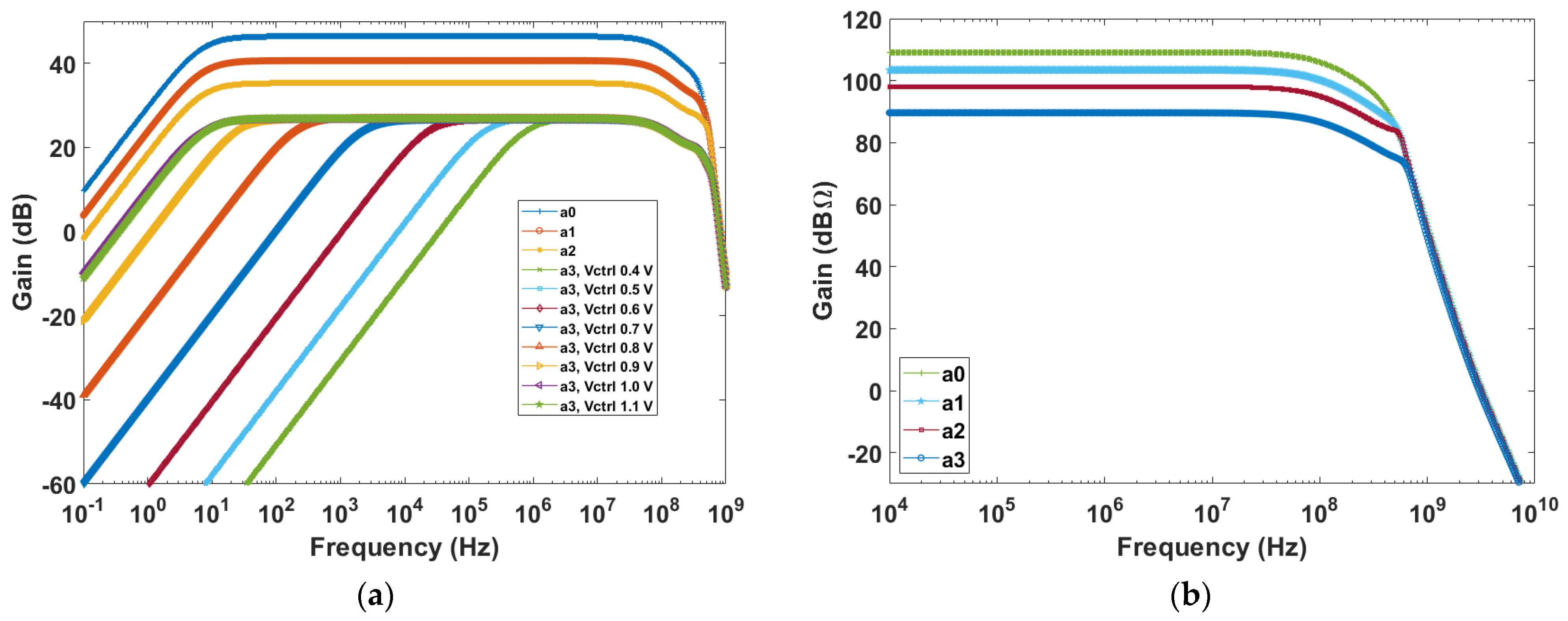
The complete cascaded structure shown in Figure 3 presents a 27–46 dB programmable gain (a3 to a0) in V-mode and a bandwidth (BW) between 112.6 MHz and 104.7 MHz (Figure 7a) at minimum and maximum gain, respectively, considering a CLoad = 50 fF. In C-mode, a gain from 89.6 dBΩ (a3) to 109.2 dBΩ (a0) and a bandwidth of 100 MHz and 95 MHz, respectively, is shown in Figure 7b, considering a CLoad = 50 fF. Figure 7a also shows the fc,H variation at minimum gain (a3) sweeping Vctrl. In this way, not only the gain but also the frequency operation range is controlled to the frequency range of interest for each application, while removing the low frequency noise to obtain optimum performance.
3.2. Temperature Dependence
The temperature behaviour of the LNA is presented in Figure 8, with a temperature range from −40 °C to 60 °C. Figure 8a presents the frequency and gain dependence with temperature in voltage mode (0.017 dB/°C, 128 kHz/°C), while Figure 8b presents the corresponding frequency and gain dependence with temperature while operating in current mode (400 µdB/°C, 35.6 kHz/°C).
The temperature behaviour of the VGA is presented in Figure 9 with a temperature range from −40 °C to 60 °C for both maximum (a0) and minimum (a3) gains. For maximum gain it shows a 15 mdB/°C, 236 kHz/°C variation, while for minimum gain, it shows a 4.5 mdB/°C, 116 kHz/°C variation.
Finally, Figure 10 shows the temperature dependence for both maximum (a0) and minimum (a3) gain configurations, displaying in V-mode gain variations of 22 mdB/°C (4.1% for a3 on) and 23.4 mdB/°C (4.4% for a0 on), and bandwidth variations of 52 kHz/°C (2.3%) and 49 kHz/°C (2.3%), respectively; C-mode renders gain variations of 10 mdB/°C (0.56% for a3 on) and 12 mdB/°C (0.55% for a3 on) and constant bandwidth for both a0 and a3.
3.3. Transient Results
In this section, we report on the transient behaviour of the cascaded structure as a complement to the frequency response of the previous section.
In Figure 11, we present the transient simulation in V-mode for both maximum and minimum gain configurations and at 8 Hz (Figure 11a), 20 MHz (Figure 11b) and 100 MHz (Figure 11c), respectively. Figure 12 shows the corresponding transient simulations for the C-mode, again at maximum and minimum gain configurations and at 8 Hz (Figure 12a), 20 MHz (Figure 12b) and 100 MHz (Figure 12c), respectively.
The system is excited with a 1 mV and a 1 µA amplitude input signal and is used in V-mode and C-mode. As can be seen, at 8 Hz and 100 MHz, the output signal is less amplified since we are reaching the cut-off frequencies and the gain is already being reduced. A closer look at these graphs shows, in C-mode, a slight phase offset and a change in the DC level at very low frequencies.
3.4. Corner Simulations
Corner simulations were carried out for the complete front-end two-stage structure at room temperature (Figure 13). In V-mode, the highest gain variation is 0.18 dB (0.67% for a0) and 0.24 dB (0.52% for a3), corresponding with a bandwidth variation of 2.6 MHz (2.48%) for maximum gain configuration and constant bandwidth for minimum gain configuration. In C-mode, the largest gain variation is 1.1 dB (1.22% for a0) and 1.5 dB (1.37% for a3), keeping a constant bandwidth.
3.5. THD and Noise
Figure 14 shows the THD for the LNA both in V-mode (with Vctrl = 1.1 V) and C-mode (Figure 14a), and the VGA with maximum and minimum gain (Figure 14b).
Considering the LNA, with a sinusoidal signal at frequency fin ≈ fc,BW/5, output amplitudes up to 277 mVpp and 390 mVpp with voltage and current input signals, respectively, results in a THD < −40 dB (1%), and noise spectral densities (NSDs), referring to the input over the frequency operating range, of 9.5 nV/√Hz (worst case) and 3.8 pA/√Hz are obtained for V-mode and C-mode, respectively (Figure 14a). The THD for the VGA is shown in Figure 14b, showing output amplitudes up to 563 mVpp (a0, maximum gain) and 351 mVpp (a3, minimum gain), and NSDs of 8 nV/√Hz (a0) and 54 nV/√Hz (a3).
Figure 15 shows the THD for the entire system. It reports values below –40 dB (1%), for peak-to-peak output amplitudes up to 1.97 Vpp and 825 mVpp (in voltage mode and for a0 and a3 configurations, respectively) and output amplitudes up to 1.99 Vpp and 2.58 Vpp (in current mode and for a0 and a3 configurations, respectively).
The NSD over the full bandwidth is 18.1 nV/√Hz and 20 nV/√Hz (in voltage mode, with Vctrl= 1.1 V and for a0 and a3 configurations, respectively) and 13 pA/√Hz and 14 pA/√Hz (in current mode and for a0 and a3 configurations, respectively).
4. Summary and Comparison
Although the presented work here is limited to post-layout simulation results, and therefore, cannot be compared on equal ground to other experimental results, a comparison between the reported architecture in this paper and previously reported works —both experimental, post-layout and simulated (schematic) results— featuring similar specifications is shown in Table 1.
For a better comparison, different figures of merit (FoMs) are used [24,25,27]. The first one is a modified version of the dynamic range, where instead of weighing the linearity/noise ratio, it also accounts for the THD. In this way, not only is the linearity range accounted for, but it also shows how good the integrity of the signal is. The NSD is expressed in V(A)/√Hz for V-mode (or C-mode), so we can also account for the noise/BW ratio of the different works reviewed. It is given by:
The second one reflects the relation between power consumption and the gain/bandwidth performance. The total area was not considered, although it is believed that it would help to compare the different proposals; however, since many of the reviewed works do not present this value, we chose to omit it to be able to compare it with the greatest number of works possible. It is given by:
Finally, the well-known noise efficiency factor (NEF) was also used as a comparison method:
with Vin,RMS as the input-referred noise and Iq as the consumed current.
With these FoMs, a higher value indicates better achieved trade-off performance, while for the NEF, the closer to unity, the better the noise performance is.
Bearing in mind the differences between the reported works, the comparison made in Table 1 reveals that our work, designed with 0.18 µm CMOS technology working at a 1.8 V supply voltage, consistent with most of the other references, demonstrates higher power efficiency compared to most previous studies, with significantly lower power consumption while maintaining a competitive performance. The area occupied by the proposed architecture is the smallest among the reported papers (together with that of [23]), indicating an efficient use of the available area.
With both voltage-mode (V-mode) and current-mode (C-mode) operation inputs, only available in few of the other reviewed works, it achieves competitive gain levels across a wide frequency range making it suitable for diverse applications. The good linearity and NSD of the proposed architecture contribute to its high-performance characteristics. The low NSD values reflect the reduced noise contribution due to the predominant noise of the LNA stage, enhancing signal fidelity. While CMRR values are not available for all references, the proposed architecture exhibits CMRR values almost two times greater than the reported ones.
As for the FoMs proposed, this work shows an excellent balance between key performance metrics such as linearity, noise, power consumption, gain and frequency range. The NEF values are within similar values in V-mode, while they are lower in C-mode compared with [22], which is the only paper providing noise for C-mode. This suggests enhanced sensitivity in signal-processing applications.
5. Conclusions
The results of this work demonstrate the efficacy of the proposed architecture in achieving high-performance specifications while offering improved power efficiency and compact area. Corner simulations have shown the robustness of the proposed architecture across varying operating conditions, while voltage dependence was not considered, as a low dropout regulator (LDO) will be used in dual-phase synchronous demodulation structures to provide a stable supply voltage.
The proposed architecture, based on two cascaded TC-TI amplification stages, has proven to be an efficient solution enabling programmable gains alongside achieving high frequencies. By employing two stages with a common core, the architecture accelerates design processes and enhances efficiency. This approach minimizes the adjustments required to transition from a fixed-gain, low-noise stage with either voltage or current input to a variable gain stage.
A high-performance versatile front-end amplifier was designed in 180 nm CMOS technology, with a power consumption of 360.5 μW at a 1.8 V power supply and a silicon area below 0.0177 mm2. It was specifically designed to support both voltage and current input signals, suitable for low-voltage low-power impedance spectroscopy applications up to the 100 MHz range, with a good trade-off between gain, frequency range and power-area consumption, reporting a 26.8–46.4 dB (89.6–109.2 dBΩ) with a 100 MHz bandwidth (>95 MHz for C-mode). Compared to the state-of-art solutions, it is a competitive solution for low-power on-chip devices, meeting the required stringent constraints which have become more critical for forthcoming multichannel IS read-outs.
As the main drawback, it should be noted that the BW in current mode reaches 95 MHz, remaining slightly below the 100 MHz target, although this could be solved simply by slightly reducing the load capacity.
Author Contributions
Conceptualization and methodology, J.P.-B., B.C.-L. and N.M.; design and implementation, J.P.-B.; analysis and validation, J.P.-B.; formal analysis, J.P.-B., B.C.-L. and N.M.; writing—original draft preparation, J.P.-B.; writing—review and editing, J.P.-B., B.C.-L. and N.M.; supervision, B.C.-L. and N.M.; funding acquisition, B.C.-L. and N.M. All authors have read and agreed to the published version of the manuscript.
Funding
This work was partially supported by the Ministerio de Ciencia e Innovación, grants PID2019-106570RB-I00 (AEI/10.13039/501100011033), PID2022-138785OB-I00 (MCIN/AEI/10.13039/501100011033/FEDER, UE).
Data Availability Statement
Data are contained within the article.
Conflicts of Interest
The authors declare no conflicts of interest.
References
- Liu, J.T.; Settu, K.; Tsai, J.-Z.; Chen, C.-J. Impedance sensor for rapid enumeration of E. coli in milk samples. Electrochim. Acta 2015, 182, 89–95. [Google Scholar] [CrossRef]
- Sitkov, N.; Zimina, T.; Soloviev, A.V. Development of Impedimetric Sensor for E. coli M-17 Antibiotic Susceptibility Testing. In Proceedings of the IEEE Conference of Russian Young Researchers in Electrical and Electronic Engineering (EIConRus), Moscow, Rusia, 29 January–1 February 2018. [Google Scholar]
- Mansoorifar, A.; Koklu, A.; Ma, S.; Raj, G.V.; Beskok, A. Electrical Impedance Measurements of Biological Cells in Response to External Stimuli. Anal. Chem. 2018, 90, 4320–4327. [Google Scholar] [CrossRef] [PubMed]
- Gadermaier, B.; Hogrefe, K.; Heitjans, P.; Wilkening, M. Broadband impedance spectroscopy of Li4Ti5O12: From nearly constant loss effects to long-range ion dynamics. J. Inorg. Gen. Chem. 2021, 647, 2167–2171. [Google Scholar] [CrossRef]
- Kanoun, O. Impedance Spectroscopy: Advanced Applications: Battery Research, Bioimpedance, System Design; Walter de Gruyter GmbH & Co KG: Berlin, Germany, 2018. [Google Scholar]
- Van Eijnatten, M.A.; Van Rijssel, M.J.; Peters, R.J.; Verdaasdonk, R.M.; Meijer, J.H. Comparison of cardiac time intervals between echocardiography and impedance cardiography at various heart rates. J. Electr. Bioimpedance 2019, 5, 2–8. [Google Scholar] [CrossRef]
- Pandey, S.; Kumar, D.; Parkash, O.; Pandey, L. Impedance Spectroscopy: A Powerful Technique for Study of Electronic Ceramics. In Ceramic Materials—Synthesis, Characterization, Applications and Recycling; IntechOpen: London, UK, 2019. [Google Scholar]
- Roy, D.; Adhikary, A. Detection of Ripening stage of Banganapalle Mango using KNN method on PCA-reduced EIS Data. In Proceedings of the 2023 IEEE International Instrumentation and Measurement Technology Conference (I2MTC), Kuala Lumpur, Malaysia, 22–25 May 2023; pp. 1–5. [Google Scholar] [CrossRef]
- Thenaisie, G.; Brivio, C. EIS-Based Hysteresis Modelling of LFP Cells. In Proceedings of the 2023 International Conference on Clean Electrical Power (ICCEP), Terrasini, Italy, 27–29 June 2023; pp. 372–377. [Google Scholar] [CrossRef]
- Geng, A.; Hu, H.; Peng, Y.; Zhao, Z.; He, Z.; Gao, S. Wideband Measurement Approach for EIS of Lithium-Ion Batteries Using Low-Frequency Concentrated Disturbance. IEEE Trans. Ind. Electron. 2024, 71, 4851–4860. [Google Scholar] [CrossRef]
- Temiz, Y.; Lovchik, R.D.; Kaigala, G.V.; Delamarche, E. Lab-on-a-chip devices: How to close and plug the lab? Microelectron. Eng. 2015, 132, 156–175. [Google Scholar] [CrossRef]
- Chowdhury, D.; Chattopadhyay, M. Study and Classification of Cell Bio-Impedance Signature for Identification of Malignancy Using Artificial Neural Network. IEEE Trans. Instrum. Meas. 2021, 70, 2505908. [Google Scholar] [CrossRef]
- Lopez-Martin, A.; Garde, M.P.; Algueta-Miguel, J.M.; Beloso-Legarra, J.; Carvajal, R.G.; Ramirez-Angulo, J. Energy-Efficient Amplifiers Based on Quasi-Floating Gate Techniques. Appl. Sci. 2021, 11, 3271. [Google Scholar] [CrossRef]
- Carrillo, J.M.; Domínguez, M.A.; Pérez-Aloe, R.; de la Cruz Blas, C.A.; Duque-Carrillo, J.F. Low-power wide-bandwidth CMOS indirect current feedback instrumentation amplifier. AEU—Int. J. Electron. Commun. 2020, 123, 153299. [Google Scholar] [CrossRef]
- Corbacho, I.; Carrillo, J.M.; Ausín, J.L.; Domínguez, M.Á.; Pérez-Aloe, R.; Duque-Carrillo, J.F. Compact CMOS Wideband Instrumentation Amplifiers for Multi-Frequency Bioimpedance Measurement: A Design Procedure. Electronics 2022, 11, 1668. [Google Scholar] [CrossRef]
- Ashayeri, M.; Yavari, M. A front-end amplifier with tunable bandwidth and high value pseudo resistor for neural recording implants. Microelectron. J. 2022, 119, 105333. [Google Scholar] [CrossRef]
- Corbacho, I.; Carrillo, J.M.; Ausín, J.L.; Domínguez, M.Á.; Pérez-Aloe, R.; Duque-Carrillo, J.F. A Fully-Differential CMOS Instrumentation Amplifier for Bioimpedance-Based IoT Medical Devices. J. Low Power Electron. Appl. 2023, 13, 3. [Google Scholar] [CrossRef]
- Cheon, S.-I.; Choi, H.; Kang, H.; Suh, J.-H.; Park, S.; Kweon, S.-J.; Je, M.; Ha, S. Impedance-Readout Integrated Circuits for Electrical Impedance Spectroscopy: Methodological Review. IEEE Trans. Biomed. Circuits Syst. 2024, 18, 215–232. [Google Scholar] [CrossRef] [PubMed]
- Xu, J.; Hong, Z. Low Power Bio-Impedance Sensor Interfaces: Review and Electronics Design Methodology. IEEE Rev. Biomed. Eng. 2022, 15, 23–35. [Google Scholar] [CrossRef] [PubMed]
- Schrunder, A.D.F.; Rusu, A. A Mixer-First Analog Front-End for Dry-Electrode Bioimpedance Spectroscopy. In Proceedings of the 2023 IEEE Biomedical Circuits and Systems Conference (BioCAS), Toronto, ON, Canada, 19–21 October 2023; pp. 1–5. [Google Scholar] [CrossRef]
- Kim, J.; Ko, H. Reconfigurable Voltage/Current Readout Instrumentation Amplifier for Cardiovascular Health Monitoring. In Proceedings of the IEEE International Symposium on Circuits and Systems (ISCAS), Florence, Italy, 27–30 May 2018; pp. 1–4. [Google Scholar] [CrossRef]
- Kim, J. Simultaneous Voltage and Current Measurement Instrumentation Amplifier for ECG and PPG Monitoring. Electronics 2021, 10, 679. [Google Scholar] [CrossRef]
- Rao, A.; Teng, Y.-C.; Schaef, C.; Murphy, E.K.; Arshad, S.; Halter, R.J.; Odame, K. An Analog Front End ASIC for Cardiac Electrical Impedance Tomography. IEEE Trans. Biomed. Circuits Syst. 2018, 12, 729–738. [Google Scholar] [CrossRef] [PubMed]
- Pérez–Bailón, J.; Calvo, B.; Medrano, N. Low-Power CMOS Amplifiers for Wideband Impedance Spectroscopy Applications. In Proceedings of the 37th Conference on Design of Circuits and Integrated Circuits (DCIS), Pamplona, Spain, 16–18 November 2022; pp. 1–6. [Google Scholar] [CrossRef]
- Gupta, S.; Mehra, R.; Sharma, S. Design and Analysis of Flipped Voltage Follower for Different Aspect Ratio. Int. J. Comput. Appl. 2016, 143, 29–32. [Google Scholar] [CrossRef]
- Márquez, A.; Medrano, N.; Calvo, B.; Pérez-Bailón, J. A Dual Synchronous Demodulator for Phase Sensitive Detection Applications. In Proceedings of the 2020 IEEE International Instrumentation and Measurement Technology Conference (I2MTC), Dubrovnik, Croatia, 25–28 May 2020; pp. 1–6. [Google Scholar]
- Mondal, S.; Hall, D.A. An ECG chopper amplifier achieving 0.92 NEF and 0.85 PEF with AC-coupled inverter-stacking for noise efficiency enhancement. In Proceedings of the IEEE International Symposium on Circuits and Systems (ISCAS), Baltimore, MD, USA, 28–31 May 2017; pp. 1–4. [Google Scholar] [CrossRef]
Figure 1.
Analog dual-phase synchronous demodulation basic structure.

Figure 2.
Diagram of the reconfigurable, fully differential proposed amplifier structure.

Figure 3.
Proposed reconfigurable, fully differential two-stage amplifier and sizes of the different elements.
Figure 3.
Proposed reconfigurable, fully differential two-stage amplifier and sizes of the different elements.

Figure 4.
Layout designed for the reconfigurable, fully differential two-stage amplifier.

Figure 5.
Gain vs. frequency response of the LNA: (a) voltage and (b) current mode.

Figure 6.
Gain vs. frequency response of the VGA.

Figure 7.
Gain vs. frequency of the complete amplifier: (a) voltage and (b) current mode.

Figure 8.
Temperature response of the LNA for (a) voltage and (b) current mode.

Figure 9.
Temperature response of the VGA at different temperatures (from −40 °C to 60 °C) for maximum and minimum gain configurations.
Figure 9.
Temperature response of the VGA at different temperatures (from −40 °C to 60 °C) for maximum and minimum gain configurations.

Figure 10.
Temperature response of the complete amplifier at different temperatures (from −40 °C to 60 °C) with maximum and minimum gain configurations for (a) voltage and (b) current mode.
Figure 10.
Temperature response of the complete amplifier at different temperatures (from −40 °C to 60 °C) with maximum and minimum gain configurations for (a) voltage and (b) current mode.

Figure 11.
Transient behaviour of the proposed amplifier in V-mode, showing the output for a 1 mV input signal and for maximum and minimum gain configurations. (a) fin = 8 Hz; (b) fin = 100 MHz; and (c) fin = fc/5 = 20 MHz.
Figure 11.
Transient behaviour of the proposed amplifier in V-mode, showing the output for a 1 mV input signal and for maximum and minimum gain configurations. (a) fin = 8 Hz; (b) fin = 100 MHz; and (c) fin = fc/5 = 20 MHz.

Figure 12.
Transient behaviour of the proposed amplifier in C-mode, showing the output for a 1 µA input signal and for maximum and minimum gain configurations: (a) fin = 8 Hz; (b) fin = 100 MHz; and (c) fin = fc/5 = 20 MHz.
Figure 12.
Transient behaviour of the proposed amplifier in C-mode, showing the output for a 1 µA input signal and for maximum and minimum gain configurations: (a) fin = 8 Hz; (b) fin = 100 MHz; and (c) fin = fc/5 = 20 MHz.

Figure 13.
Corner analysis of the cascaded structure for maximum (a0) and minimum (a3) gain configurations for (a) voltage and (b) current mode.
Figure 13.
Corner analysis of the cascaded structure for maximum (a0) and minimum (a3) gain configurations for (a) voltage and (b) current mode.

Figure 14.
Total harmonic distortion (THD) vs. output amplitude for voltage and current modes of (a) the LNA and (b) the VGA with 26 dB (a0) and 6 dB (a3) gains.
Figure 14.
Total harmonic distortion (THD) vs. output amplitude for voltage and current modes of (a) the LNA and (b) the VGA with 26 dB (a0) and 6 dB (a3) gains.

Figure 15.
THD of the front-end amplifier vs. output amplitude in both voltage and current mode and with a0 and a3 gain configurations.
Figure 15.
THD of the front-end amplifier vs. output amplitude in both voltage and current mode and with a0 and a3 gain configurations.


Table 1.
Comparison with previously reported works.
| Parameter | [22]’18 | [14]’20 | [26]’20 | [23]’21 | [15]’22 | [16]’22 | [17]’23 | This Work (V-Mode) | This Work (C-Mode) |
|---|---|---|---|---|---|---|---|---|---|
| Result | Exp | Sim | Sim | Exp | Exp | Post-layout | Exp | Post-layout | Post-layout |
| Input mode | V/C | V | V | V/C | V (2) | V | V | V/C | V/C |
| CMOS (µm) | 0.18 | 0.35 | 0.18 | 0.18 | 0.18 | 0.18 | 0.18 | 0.18 | 0.18 |
| Supply (V) | 1.6 | 3 | 1.8 | 1.8 | 1.8 | 1 | 1.8 | 1.8 | 1.8 |
| Power (µW) | 72 (1) | 751.8 | 36.1 | 55.8 (1) | 394.7 | 3.6 | 479.5 | 360.5 | 360.5 |
| Area (mm2) | ** | ** | ** | 0.0177 | 0.0291 | 0.048 | 0.0304 | 0.0177 | 0.0177 |
| Gain (dB) | 37 dB/117 dBΩ | 34 | 0–20 | 55 dB/118 dBΩ (1) | 11.4 | 45/55 | 11.4 | 26.8–46.4 | 89.6–109.2 |
| Freq. range (Hz) | 0.1–100 | 7.6 M | 0.1–1 M | 1–200/0.25–15 | 8 M | 0.8–4.1 k/300–8.2 k | 5.83 M | 6.9− > 100 M | 0.1− > 95 M |
| Linearity (Vout.pp) @ THD (dB) | 0.035 @ −57.9 0.142 @ −61.7 | 0.01 @−57.4 | ** | ** | 0.02 @ −61.6 | 0.001 @ −46.32 | 0.02 @ −64.9 | 1.97–0.83 @ −40 | 1.99–2.58 @ −40 |
| NSD (V(A)/√Hz) | 271.4 nV/38.4 pA (1) | 11.8 nV | 189.6 nV | 276 nV/44.8 pA | 32.5 nV (1) | 26.39 nV/23.19 nV (1) | 35.78 nV | 20 nV–18 nV | 14.4 pA–13 pA |
| CMRR (dB) @ Hz | ** | 99.5 @DC | 55.3 @ ** | ** | 80.6 @ DC | 98.28 @ 50 | 73.3 @ DC | 202–202 @100 k | 191–214 @100 k |
| FoM1 (dB) | 160.1–165.3 | 176 | ** | ** | 177.4 | 137.9/139 | 179.8 | 119.9–193.3 | 262.8–267 |
| FoM2 (dBxMHz/µW) | 98.23 µ/0.98 | 343.7 m | 27.8 m–0.278 | 2 m/0.21 | 0.231 | 0.05/0.125 | 4.08 | 8.37–13.48 | 24.85–28.78 |
| NEF | 155.8/22 m | 7.2 | 73.01 | ** | 26.3 | 1.7 | 21.3 | 10.28–9.64 | 7.84 m–7.27 m |
** Not Available; (1) Values estimated; (2) Pseudo-Differential.
Disclaimer/Publisher’s Note: The statements, opinions and data contained in all publications are solely those of the individual author(s) and contributor(s) and not of MDPI and/or the editor(s). MDPI and/or the editor(s) disclaim responsibility for any injury to people or property resulting from any ideas, methods, instructions or products referred to in the content. |
© 2024 by the authors. Licensee MDPI, Basel, Switzerland. This article is an open access article distributed under the terms and conditions of the Creative Commons Attribution (CC BY) license (https://creativecommons.org/licenses/by/4.0/).
Share and Cite
MDPI and ACS Style
Pérez-Bailón, J.; Calvo-López, B.; Medrano, N. Reconfigurable Low-Power CMOS Amplifier Stages for Broadband Impedance Spectroscopy. Electronics 2024, 13, 1674. https://doi.org/10.3390/electronics13091674
AMA Style
Pérez-Bailón J, Calvo-López B, Medrano N. Reconfigurable Low-Power CMOS Amplifier Stages for Broadband Impedance Spectroscopy. Electronics. 2024; 13(9):1674. https://doi.org/10.3390/electronics13091674
Chicago/Turabian StylePérez-Bailón, Jorge, Belén Calvo-López, and Nicolás Medrano. 2024. "Reconfigurable Low-Power CMOS Amplifier Stages for Broadband Impedance Spectroscopy" Electronics 13, no. 9: 1674. https://doi.org/10.3390/electronics13091674
Note that from the first issue of 2016, this journal uses article numbers instead of page numbers. See further details here.