A Comprehensive Review of Recent Progress on GaN High Electron Mobility Transistors: Devices, Fabrication and Reliability

Abstract
:1. Introduction
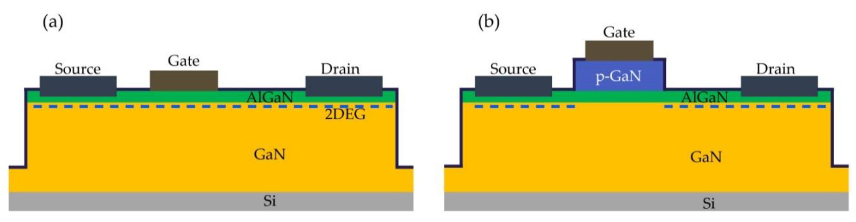
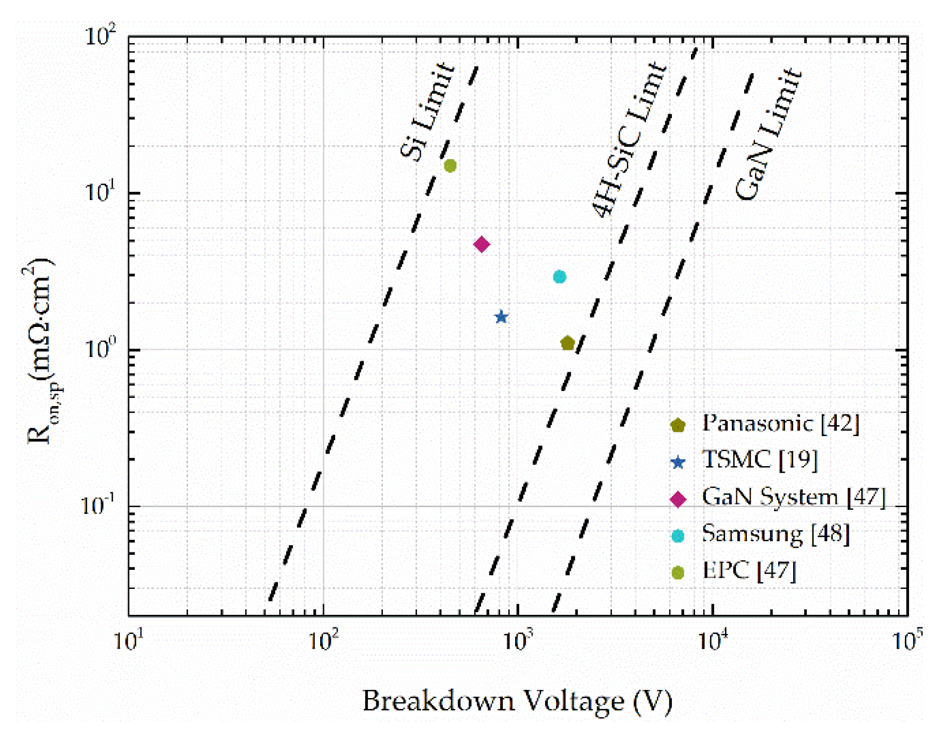
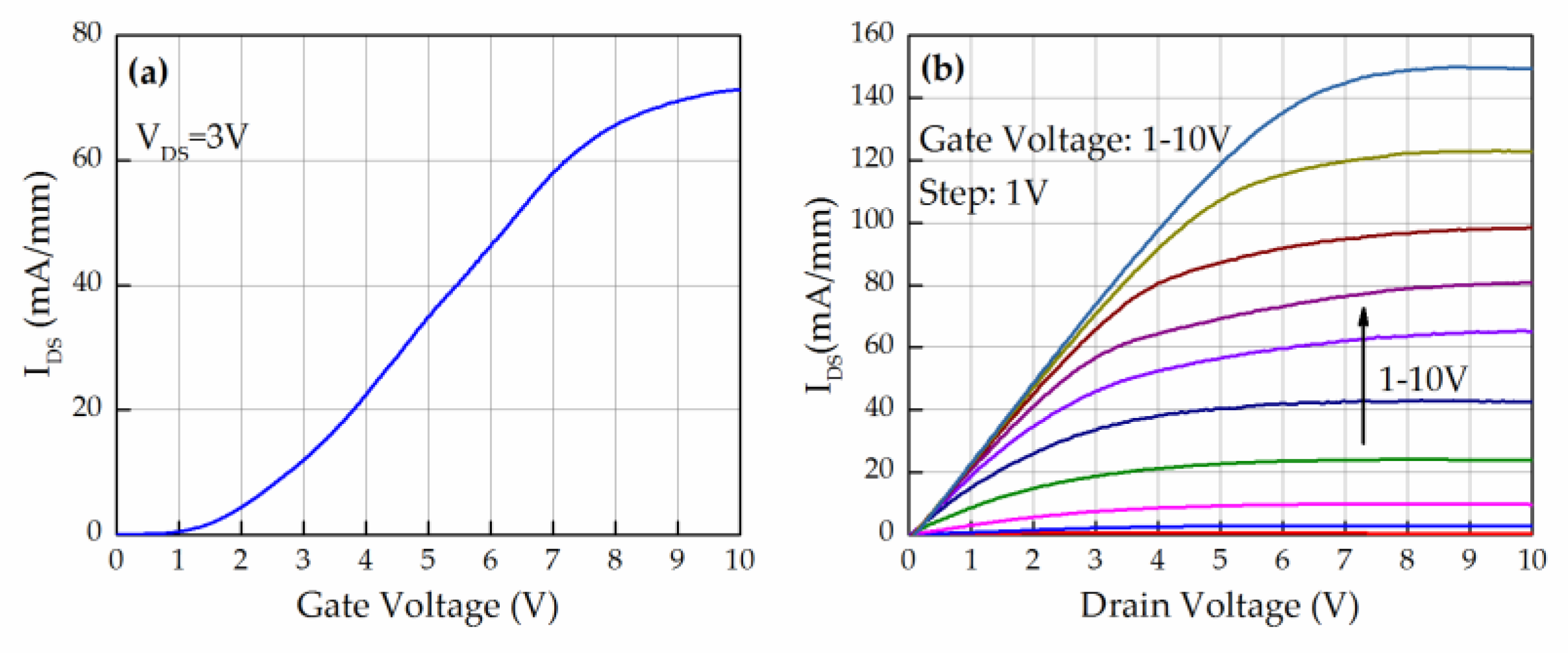
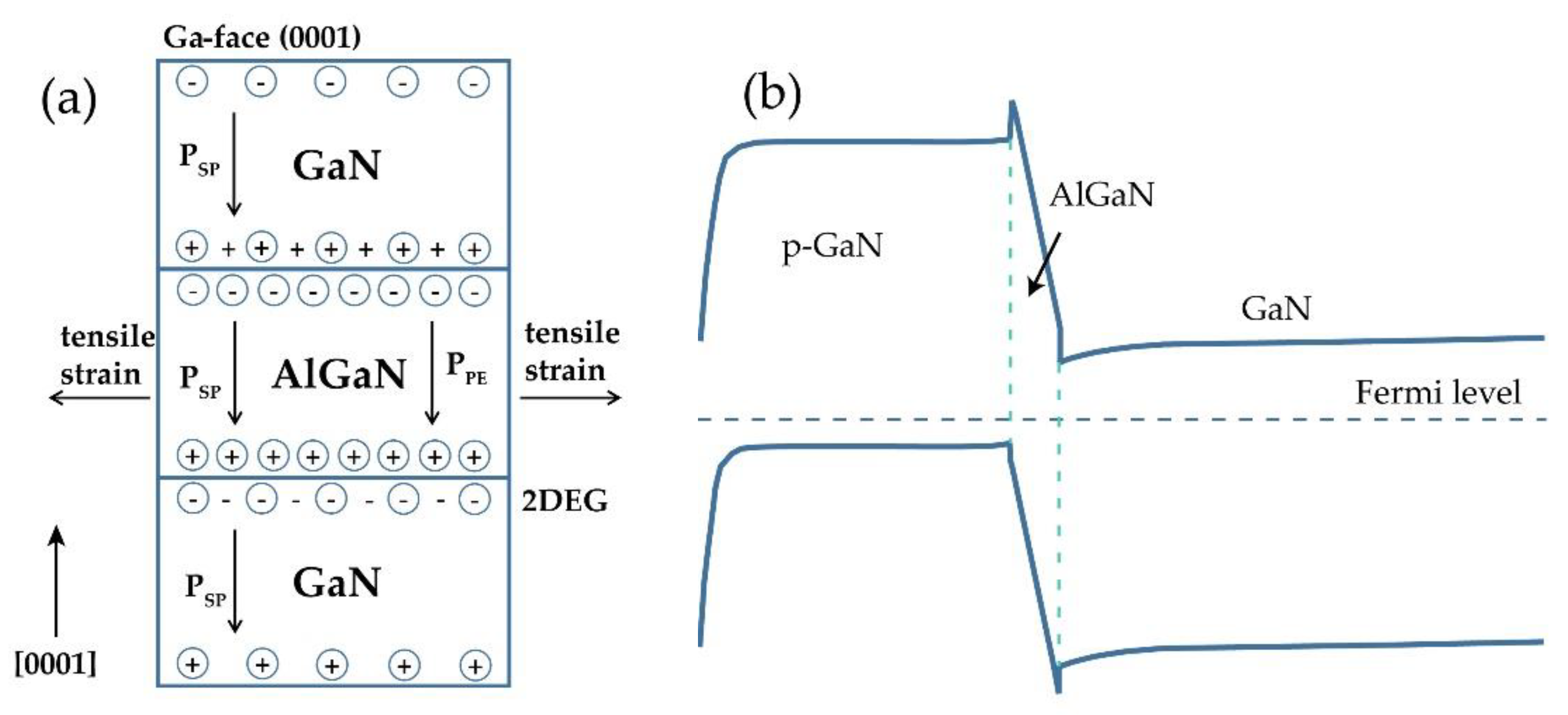
2. AlGaN/GaN HEMT Device
3. AlGaN/GaN HEMT Device Fabrication
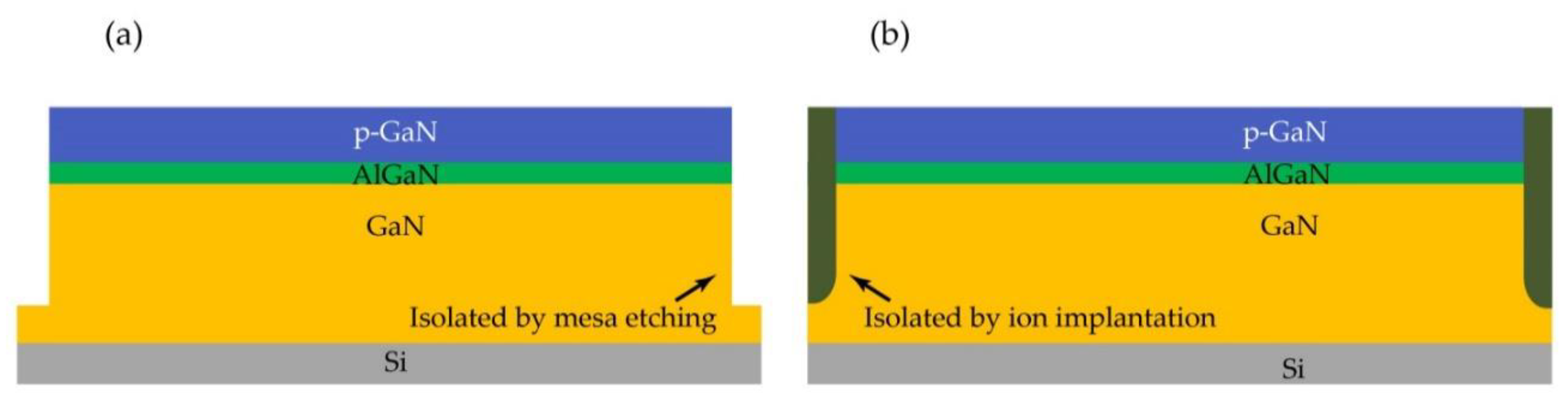
3.1. Device Isolation
3.1.1. Mesa Etching
3.1.2. Ion Implantation
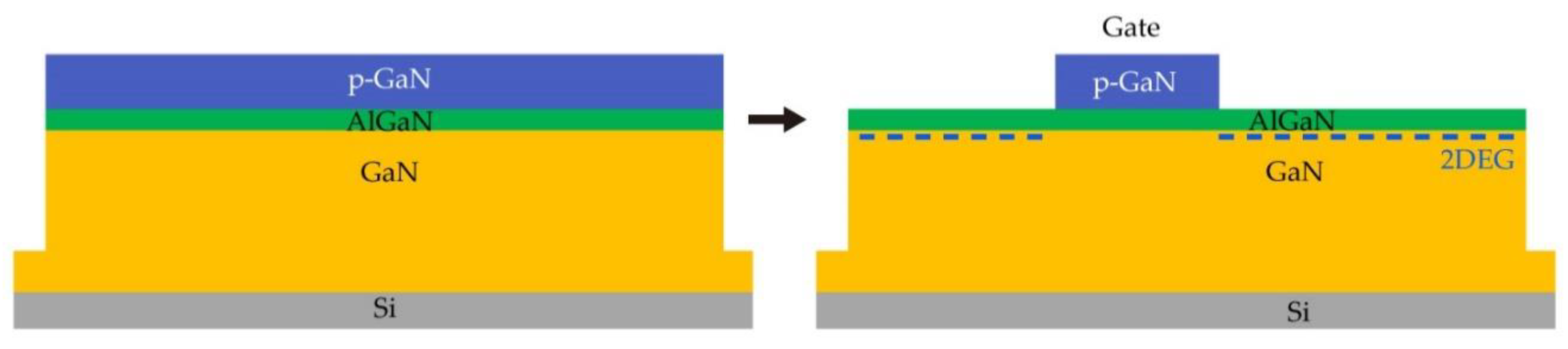
3.2. P-GaN Gate Formation
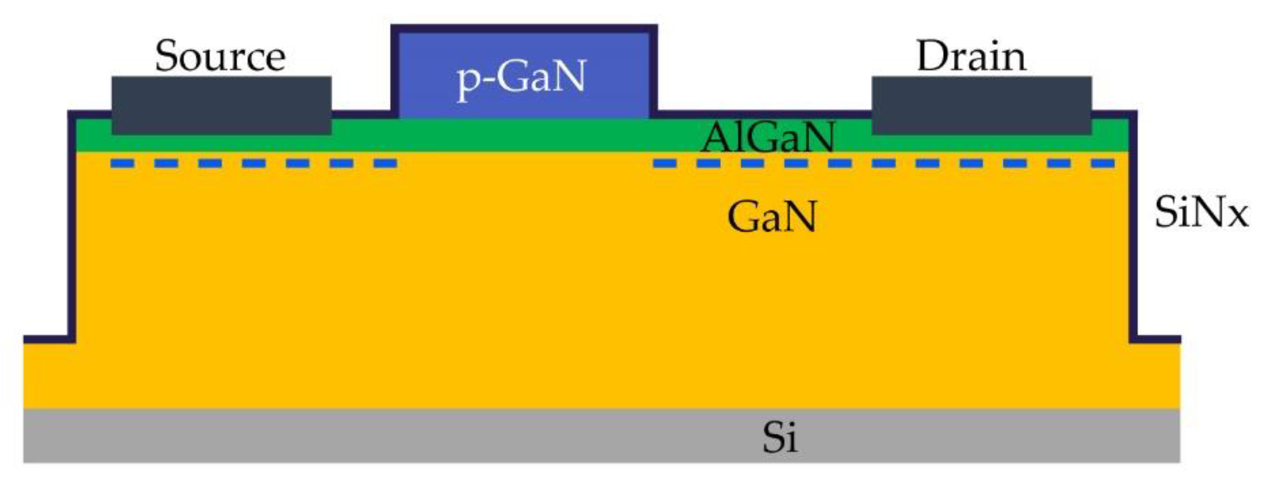
3.3. Ohmic Contacts for Source and Drain
3.4. Contact for Gate
3.5. Surface Passivation
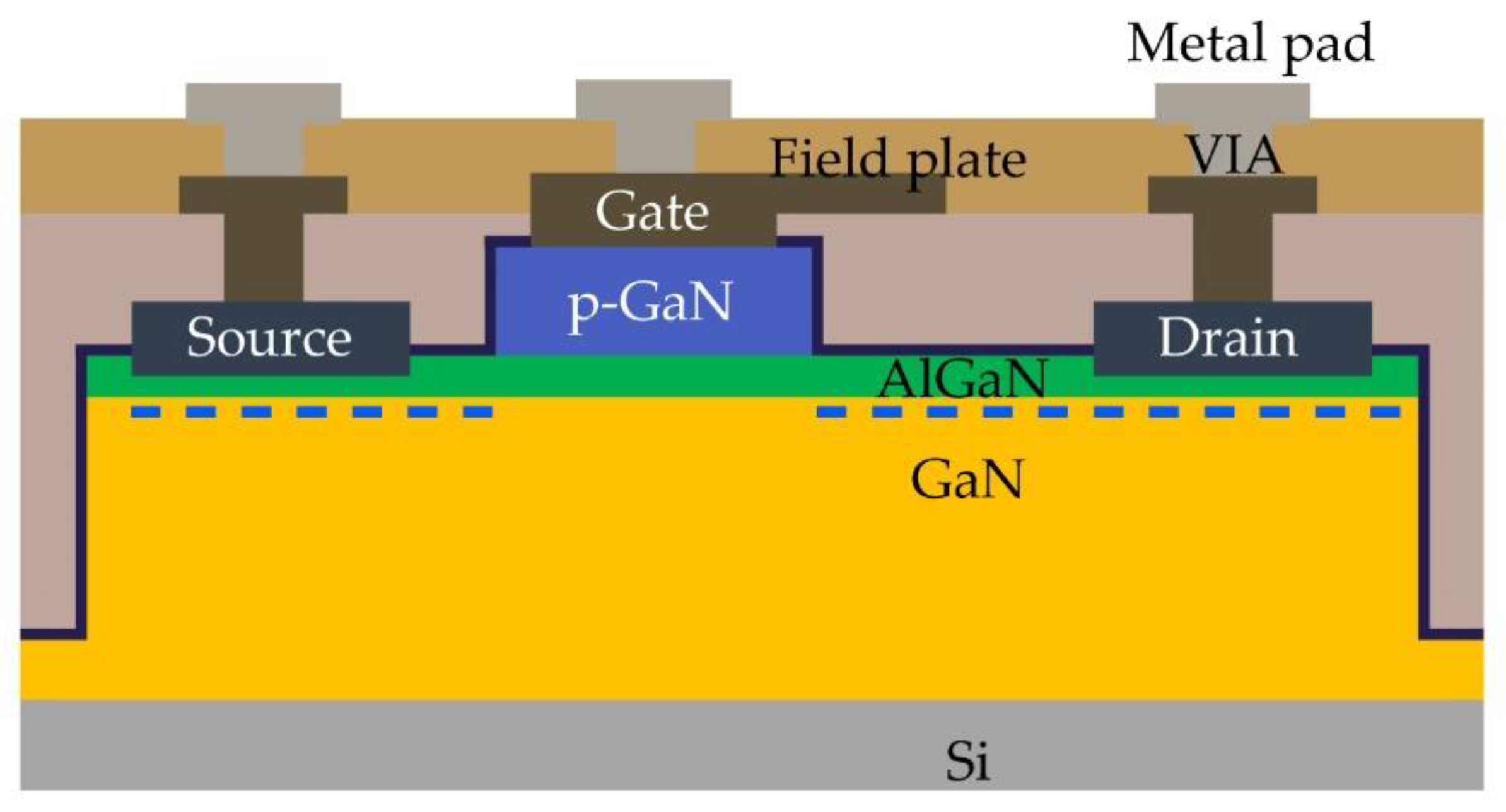
3.6. Field Plates
4. AlGaN/GaN Device Simulation
5. Summary
Author Contributions
Funding
Conflicts of Interest
References
- Treu, M.; Vecino, E.; Pippan, M.; Haberlen, O.; Curatola, G.; Deboy, G.; Kutschak, M.; Kirchner, U. The role of silicon, silicon carbide and gallium nitride in power electronics. In Proceedings of the 2012 International Electron Devices Meeting, San Francisco, CA, USA, 10–13 December 2012; pp. 7.1.1–7.1.4. [Google Scholar]
- Ueda, D. Renovation of power devices by GaN-based materials. In Proceedings of the 2015 IEEE International Electron Devices Meeting (IEDM), Washington, DC, USA, 7–9 December 2015; pp. 16.4.1–16.4.4. [Google Scholar]
- Piedra, D.; Lu, B.; Sun, M.; Zhang, Y.; Matioli, E.; Gao, F.; Chung, J.W.; Saadat, O.; Xia, L.; Azize, M.; et al. Advanced power electronic devices based on Gallium Nitride (GaN). In Proceedings of the 2015 IEEE International Electron Devices Meeting (IEDM), Washington, DC, USA, 7–9 December 2015; pp. 16.6.1–16.6.4. [Google Scholar]
- Deboy, G.; Treu, M.; Haeberlen, O.; Neumayr, D. Si, SiC and GaN power devices: An unbiased view on key performance indicators. In Proceedings of the 2016 IEEE International Electron Devices Meeting (IEDM), San Francisco, CA, USA, 3–7 December 2016; pp. 20.2.1–20.2.4. [Google Scholar]
- Yu, H.; Duan, T. Gallium Nitride Power Devices; Pan Stanford: Singapore, 2017. [Google Scholar]
- Lidow, A.; Strydom, J.; de Rooij, M.; Reusch, D. GaN Transistors for Efficient Power Conversion; Willey: New York, NY, USA, 2015. [Google Scholar]
- Meneghini, M.; Gaudenzio, M.; Zanoni, E. Power GaN Devices—Materials, Applications and Reliability; Springer: New York, NY, USA, 2017. [Google Scholar]
- Chen, K.J.; Haberlen, O.; Lidow, A.; Tsai, C.L.; Ueda, T.; Uemoto, Y.; Wu, Y. GaN-on-Si Power Technology: Devices and Applications. IEEE Trans. Electron Devices 2017, 64, 779–795. [Google Scholar] [CrossRef]
- Tsai, C.-L.; Wang, Y.-H.; Kwan, M.H.; Chen, P.C.; Yao, F.W.; Liu, S.C.; Yu, J.L.; Yeh, C.L.; Su, R.Y.; Wang, W.; et al. Smart GaN platform: Performance & challenges. In Proceedings of the 2017 IEEE International Electron Devices Meeting (IEDM), San Francisco, CA, USA, 2–6 December 2017; pp. 33.1.1–33.1.4. [Google Scholar]
- Meneghesso, G.; Meneghini, M.; Zanoni, E. Gallium Nitride-Enabled High Frequency and High Efficiency Power Conversion; Springer: New York, NY, USA, 2018. [Google Scholar]
- Hyung-Seok, L.; Dong Seup, L.; Palacios, T. AlGaN/GaN High-Electron-Mobility Transistors Fabricated through a Au-Free Technology. IEEE Electron Device Lett. 2011, 32, 623–625. [Google Scholar] [CrossRef]
- Stoffels, S.; Zhao, M.; Venegas, R.; Kandaswamy, P.; You, S.; Novak, T.; Saripalli, Y.; Van Hove, M.; Decoutere, S. The physical mechanism of dispersion caused by AlGaN/GaN buffers on Si and optimization for low dispersion. In Proceedings of the 2015 IEEE International Electron Devices Meeting (IEDM), Washington, DC, USA, 7–9 December 2015; pp. 35.4.1–35.4.4. [Google Scholar]
- Marcon, D.; Saripalli, Y.N.; Decoutere, S. 200mm GaN-on-Si epitaxy and e-mode device technology. In Proceedings of the 2015 IEEE International Electron Devices Meeting (IEDM), Washington, DC, USA, 7–9 December 2015; pp. 16.2.1–16.2.4. [Google Scholar]
- Zhang, Z.; Li, B.; Tang, X.; Qian, Q.; Hua, M.; Huang, B.; Chen, K.J. Nitridation of GaN surface for power device application: A first-principles study. In Proceedings of the 2016 IEEE International Electron Devices Meeting (IEDM), San Francisco, CA, USA, 3–7 December 2016; pp. 36.2.1–36.2.4. [Google Scholar]
- Wang, J.; Cao, L.; Xie, J.; Beam, E.; McCarthy, R.; Youtsey, C.; Fay, P. High voltage vertical p-n diodes with ion-implanted edge termination and sputtered SiNx passivation on GaN substrates. In Proceedings of the 2017 IEEE International Electron Devices Meeting (IEDM), San Francisco, CA, USA, 2–6 December 2017; pp. 9.6.1–9.6.4. [Google Scholar]
- Hashizume, T.; Nishiguchi, K.; Kaneki, S.; Kuzmik, J.; Yatabe, Z. State of the art on gate insulation and surface passivation for GaN-based power HEMTs. Mater. Sci. Semicond. Process. 2018, 78, 85–95. [Google Scholar] [CrossRef]
- Kim, Z.-S.; Lee, H.-S.; Na, J.; Bae, S.-B.; Nam, E.; Lim, J.-W. Ultra-low rate dry etching conditions for fabricating normally-off field effect transistors on AlGaN/GaN heterostructures. Solid-State Electron. 2018, 140, 12–17. [Google Scholar] [CrossRef]
- Wong, K.-Y.; Lin, Y.S.; Hsiung, C.W.; Lansbergen, G.P.; Lin, M.C.; Yao, F.W.; Yu, C.J.; Chen, P.C.; Su, R.Y.; Yu, J.L.; et al. AlGaN/GaN MIS-HFET with improvement in high temperature gate bias stress-induced reliability. In Proceedings of the 2014 IEEE 26th International Symposium on Power Semiconductor Devices & IC’s (ISPSD), Waikoloa, HI, USA, 15–19 June 2014; pp. 55–58. [Google Scholar]
- Man Ho, K.; Wong, K.Y.; Lin, Y.S.; Yao, F.W.; Tsai, M.W.; Chang, Y.C.; Chen, P.C.; Su, R.Y.; Wu, C.H.; Yu, J.L.; et al. CMOS-compatible GaN-on-Si field-effect transistors for high voltage power applications. In Proceedings of the 2014 IEEE International Electron Devices Meeting (IEDM), San Francisco, CA, USA, 15–17 December 2014; pp. 17.6.1–17.6.4. [Google Scholar]
- Moens, P.; Banerjee, A.; Uren, M.J.; Meneghini, M.; Karboyan, S.; Chatterjee, I.; Vanmeerbeek, P.; Casar, M.; Liu, C.; Salih, A.; et al. Impact of buffer leakage on intrinsic reliability of 650V AlGaN/GaN HEMTs. In Proceedings of the 2015 International Electron Devices Meeting, Washington, DC, USA, 7–9 December 2015; pp. 35.2.1–35.2.4. [Google Scholar]
- Bahl, S.R.; Joh, J.; Fu, L.; Sasikumar, A.; Chatterjee, T.; Pendharkar, S. Application reliability validation of GaN power devices. In Proceedings of the International Electron Devices Meeting (IEDM), San Francisco, CA, USA, 3–7 December 2016; pp. 20.5.1–20.5.4. [Google Scholar]
- Koller, C.; Pobegen, G.; Ostermaier, C.; Pogany, D. Evidence of defect band in carbon-doped GaN controlling leakage current and trapping dynamics. In Proceedings of the 2017 International Electron Devices Meeting (IEDM), San Francisco, CA, USA, 2–6 December 2017; pp. 33.4.1–33.4.4. [Google Scholar]
- Meneghini, M.; Tajalli, A.; Moens, P.; Banerjee, A.; Stockman, A.; Tack, M.; Gerardin, S.; Bagatin, M.; Paccagnella, A.; Zanoni, E.; et al. Total suppression of dynamic-ron in AlGaN/GaN-HEMTs through proton irradiation. In Proceedings of the 2017 International Electron Devices Meeting (IEDM), San Francisco, CA, USA, 2–6 December 2017; pp. 33.5.1–33.5.4. [Google Scholar]
- Qi, Y.; Zhu, Y.; Zhang, J.; Lin, X.; Cheng, K.; Jiang, L.; Yu, H. Evaluation of LPCVD SiNx Gate Dielectric Reliability by TDDB Measurement in Si-Substrate-Based AlGaN/GaN MIS-HEMT. IEEE Trans. Electron Devices 2018, 65, 1759–1764. [Google Scholar] [CrossRef]
- Radhakrishna, U.; Lim, S.; Choi, P.; Palacios, T.; Antoniadis, D. GaNFET compact model for linking device physics, high voltage circuit design and technology optimization. In Proceedings of the 2015 International Electron Devices Meeting, Washington, DC, USA, 7–9 December 2015; pp. 9.6.1–9.6.4. [Google Scholar]
- Cornigli, D.; Reggiani, S.; Gnani, E.; Gnudi, A.; Baccarani, G.; Moens, P.; Vanmeerbeek, P.; Banerjee, A.; Meneghesso, G. Numerical investigation of the lateral and vertical leakage currents and breakdown regimes in GaN-on-Silicon vertical structures. In Proceedings of the 2015 International Electron Devices Meeting, Washington, DC, USA, 7–9 December 2015; pp. 5.3.1–5.3.4. [Google Scholar]
- Raciti, A.; Cristaldi, D.; Greco, G.; Vinci, G.; Bazzano, G. Integrated power electronics modules: Electro-thermal modeling flow and stress conditions overview. In Proceedings of the 2014 AEIT Annual Conference—From Research to Industry: The Need for a More Effective Technology Transfer (AEIT), Trieste, Italy, 18–19 September 2014; pp. 1–6. [Google Scholar]
- Wong, K.Y.R.; Kwan, M.H.; Yao, F.W.; Tsai, M.W.; Lin, Y.S.; Chang, Y.C.; Chen, P.C.; Su, R.Y.; Yu, J.L.; Yang, F.J.; et al. A next generation CMOS-compatible GaN-on-Si transistors for high efficiency energy systems. In Proceedings of the 2015 International Electron Devices Meeting, Washington, DC, USA, 7–9 December 2015; pp. 9.5.1–9.5.4. [Google Scholar]
- Di Cioccio, L.; Morvan, E.; Charles, M.; Perichon, P.; Torres, A.; Ayel, F.; Bergogne, D.; Baines, Y.; Fayolle, M.; Escoffier, R.; et al. From epitaxy to converters topologies what issues for 200 mm GaN/Si? In Proceedings of the 2015 International Electron Devices Meeting, Washington, DC, USA, 7–9 December 2015; pp. 16.5.1–16.5.4. [Google Scholar]
- Hughes, B.; Chu, R.; Lazar, J.; Boutros, K. Increasing the switching frequency of GaN HFET converters. In Proceedings of the 2015 International Electron Devices Meeting, Washington, DC, USA, 7–9 December 2015; pp. 16.7.1–16.7.4. [Google Scholar]
- Then, H.W.; Chow, L.A.; Dasgupta, S.; Gardner, S.; Radosavljevic, M.; Rao, V.R.; Sung, S.H.; Yang, G.; Fischer, P. High-K gate dielectric depletion-mode and enhancement-mode GaN MOS-HEMTs for improved OFF-state leakage and DIBL for power electronics and RF applications. In Proceedings of the 2015 International Electron Devices Meeting, Washington, DC, USA, 7–9 December 2015; pp. 16.3.1–16.3.4. [Google Scholar]
- Coffa, S.; Saggio, M.; Patti, A. SiC- and GaN-based power devices: Technologies, products and applications. In Proceedings of the 2015 International Electron Devices Meeting, Washington, DC, USA, 7–9 December 2015; pp. 16.8.1–16.8.5. [Google Scholar]
- Ishida, H.; Kajitani, R.; Kinoshita, Y.; Umeda, H.; Ujita, S.; Ogawa, M.; Tanaka, K.; Morita, T.; Tamura, S.; Ishida, M.; et al. GaN-based semiconductor devices for future power switching systems. In Proceedings of the International Electron Devices Meeting (IEDM), San Francisco, CA, USA, 3–7 December 2016; pp. 20.4.1–20.4.4. [Google Scholar]
- Lidow, A.; Reusch, D.; Glaser, J. System level impact of GaN power devices in server architectures. In Proceedings of the International Electron Devices Meeting (IEDM), San Francisco, CA, USA, 3–7 December 2016; pp. 20.3.1–20.3.4. [Google Scholar]
- Asif Khan, M.; Bhattarai, A.; Kuznia, J.N.; Olson, D.T. High electron mobility transistor based on a GaN-AlxGa1−xN heterojunction. Appl. Phys. Lett. 1993, 63, 1214–1215. [Google Scholar] [CrossRef]
- Khan, M.A.; Chen, Q.; Sun, C.J.; Yang, J.W.; Blasingame, M.; Shur, M.S.; Park, H. Enhancement and depletion mode GaN/AlGaN heterostructure field effect transistors. Appl. Phys. Lett. 1996, 68, 514–516. [Google Scholar] [CrossRef]
- Hu, X.; Simin, G.; Yang, J.; Asif Khan, M.; Gaska, R.; Shur, M.S. Enhancement mode AlGaN/GaN HFET with selectively grown pn junction gate. Electron. Lett. 2000, 36, 753–754. [Google Scholar] [CrossRef]
- Oka, T.; Nozawa, T. AlGaN/GaN Recessed MIS-Gate HFET With High-Threshold-Voltage Normally-Off Operation for Power Electronics Applications. IEEE Electron Device Lett. 2008, 29, 668–670. [Google Scholar] [CrossRef]
- Greco, G.; Iucolano, F.; Roccaforte, F. Review of technology for normally-off HEMTs with p-GaN gate. Mater. Sci. Semicond. Process. 2018, 78, 96–106. [Google Scholar] [CrossRef]
- Tanaka, K.; Morita, T.; Umeda, H.; Kaneko, S.; Kuroda, M.; Ikoshi, A.; Yamagiwa, H.; Okita, H.; Hikita, M.; Yanagihara, M.; et al. Suppression of current collapse by hole injection from drain in a normally-off GaN-based hybrid-drain-embedded gate injection transistor. Appl. Phys. Lett. 2015, 107, 163502. [Google Scholar] [CrossRef]
- Kumar, A.; De Souza, M.M. Extending the bounds of performance in E-mode p-channel GaN MOSHFETs. In Proceedings of the International Electron Devices Meeting (IEDM), San Francisco, CA, USA, 3–7 December 2016; pp. 7.4.1–7.4.4. [Google Scholar]
- Uemoto, Y.; Hikita, M.; Ueno, H.; Matsuo, H.; Ishida, H.; Yanagihara, M.; Ueda, T.; Tanaka, T.; Ueda, D. Gate Injection Transistor (GIT)—A Normally-Off AlGaN/GaN Power Transistor Using Conductivity Modulation. IEEE Trans. Electron Devices 2007, 54, 3393–3399. [Google Scholar] [CrossRef]
- Nakazawa, S.; Shih, H.; Tsurumi, N.; Anda, Y.; Hatsuda, T.; Ueda, T.; Nozaki, M.; Yamada, T.; Hosoi, T.; Shimura, T.; et al. Fast switching performance by 20 A/730 V AlGaN/GaN MIS-HFET using AlON gate insulator. In Proceedings of the 2017 IEEE International Electron Devices Meeting (IEDM), San Francisco, CA, USA, 2–6 December 2017; pp. 25.1.1–25.1.4. [Google Scholar]
- Son, D.-H.; Jo, Y.-W.; Won, C.-H.; Lee, J.-H.; Seo, J.H.; Lee, S.-H.; Lim, J.-W.; Kim, J.H.; Kang, I.M.; Cristoloveanu, S.; et al. Normally-off AlGaN/GaN-based MOS-HEMT with self-terminating TMAH wet recess etching. Solid-State Electron. 2018, 141, 7–12. [Google Scholar] [CrossRef]
- Ji, D.; Gupta, C.; Chan, S.H.; Agarwal, A.; Li, W.; Keller, S.; Mishra, U.K.; Chowdhury, S. Demonstrating >1.4 kV OG-FET performance with a novel double field-plated geometry and the successful scaling of large-area devices. In Proceedings of the 2017 International Electron Devices Meeting (IEDM), San Francisco, CA, USA, 2–6 December 2017; pp. 9.4.1–9.4.4. [Google Scholar]
- Zeng, C.; Wang, Y.-S.; Liao, X.-Y.; Li, R.-G.; Chen, Y.-Q.; Lai, P.; Huang, Y.; En, Y.-F. Reliability Investigations of AlGaN/GaN HEMTs Based on On-State Electroluminescence Characterization. IEEE Trans. Device Mater. Reliab. 2015, 15, 69–74. [Google Scholar] [CrossRef]
- Amano, H.; Baines, Y.; Beam, E.; Borga, M.; Bouchet, T.; Chalker, P.R.; Charles, M.; Chen, K.J.; Chowdhury, N.; Chu, R.; et al. The 2018 GaN power electronics roadmap. J. Phys. D Appl. Phys. 2018, 51, 163001. [Google Scholar] [CrossRef] [Green Version]
- Hwang, I.; Choi, H.; Lee, J.; Choi, H.S.; Kim, J.; Ha, J.; Um, C.-Y.; Hwang, S.-K.; Oh, J.; Kim, J.-Y.; et al. 1.6 kV, 2.9 mΩ cm2 normally-off p-GaN HEMT device. In Proceedings of the 2012 24th International Symposium on Power Semiconductor Devices and ICs, Bruges, Belgium, 3–7 June 2012; pp. 41–44. [Google Scholar]
- Wang, Z.; Zhang, B.; Chen, W.; Li, Z. A Closed-Form Charge Control Model for the Threshold Voltage of Depletion- and Enhancement-Mode AlGaN/GaN Devices. IEEE Trans. Electron Devices 2013, 60, 1607–1612. [Google Scholar] [CrossRef]
- Ning, W.; Hui, W.; Xinpeng, L.; Yongle, Q.; Tianli, D.; Lingli, J.; Iervolino, E.; Kai, C.; Hongyu, Y. Investigation of AlGaN/GaN HEMTs degradation with gate pulse stressing at cryogenic temperature. AIP Adv. 2017, 7, 095317. [Google Scholar] [Green Version]
- Meneghini, M.; Hilt, O.; Wuerfl, J.; Meneghesso, G. Technology and Reliability of Normally-Off GaN HEMTs with p-Type Gate. Energies 2017, 10, 153. [Google Scholar] [CrossRef]
- Shul, R.J.; McClellan, G.B.; Casalnuovo, S.A.; Rieger, D.J.; Pearton, S.J.; Constantine, C.; Barratt, C.; Karlicek, R.F.; Tran, C.; Schurman, M. Inductively coupled plasma etching of GaN. Appl. Phys. Lett. 1996, 69, 1119–1121. [Google Scholar] [CrossRef]
- Shul, R.J.; Vawter, G.A.; Willison, C.G.; Bridges, M.M.; Lee, J.W.; Pearton, S.J.; Abernathy, C.R. Comparison of plasma etch techniques for III–V nitrides. Solid-State Electron. 1998, 42, 2259–2267. [Google Scholar] [CrossRef]
- Sheu, J.K.; Su, Y.K.; Chi, G.C.; Jou, M.J.; Liu, C.C.; Chang, C.M.; Hung, W.C. Inductively coupled plasma etching of GaN using Cl2/Ar and Cl2/N2 gases. J. Appl. Phys. 1999, 85, 1970–1974. [Google Scholar] [CrossRef]
- Pearton, S.J.; Shul, R.J.; Ren, F. A Review of Dry Etching of GaN and Related Materials. MRS Internet J. Nitride Semicond. Res. 2014, 5, 11. [Google Scholar] [CrossRef]
- Kodera, M.; Yoshioka, A.; Sugiyama, T.; Ohguro, T.; Hamamoto, T.; Kawamoto, T.; Yamanaka, T.; Xinyu, Z.; Lester, S.; Miyashita, N. Impact of Plasma-Damaged-Layer Removal on GaN HEMT Devices. Phys. Status Solidi 2018, 215, 1700633. [Google Scholar] [CrossRef]
- Tripathy, S.; Ramam, A.; Chua, S.J.; Pan, J.S.; Huan, A. Characterization of inductively coupled plasma etched surface of GaN using Cl2/BCl3 chemistry. J. Vac. Sci. Technol. A Vac. Surf. Films 2001, 19, 2522–2532. [Google Scholar] [CrossRef]
- Pearton, S.J.; Abernathy, C.R.; Ren, F. Dry patterning of InGaN and InAlN. Appl. Phys. Lett. 1994, 64, 3643–3645. [Google Scholar] [CrossRef]
- Zhe, X.; Jinyan, W.; Jingqian, L.; Chunyan, J.; Yong, C.; Zhenchuan, Y.; Maojun, W.; Min, Y.; Bing, X.; Wengang, W.; et al. Demonstration of Normally-Off Recess-Gated AlGaN/GaN MOSFET Using GaN Cap Layer as Recess Mask. IEEE Electron Device Lett. 2014, 35, 1197–1199. [Google Scholar] [CrossRef]
- Shul, R.J.; Willison, C.G.; Bridges, M.M.; Han, J.; Lee, J.W.; Pearton, S.J.; Abernathy, C.R.; MacKenzie, J.D.; Donovan, S.M.; Zhang, L.; et al. Selective inductively coupled plasma etching of group-III nitrides in Cl2- and BCl3-based plasmas. J. Vac. Sci. Technol. A Vac. Surf. Films 1998, 16, 1621–1626. [Google Scholar] [CrossRef]
- Wakejima, A.; Ando, A.; Watanabe, A.; Inoue, K.; Kubo, T.; Osada, Y.; Kamimura, R.; Egawa, T. Normally off AlGaN/GaN HEMT on Si substrate with selectively dry-etched recessed gate and polarization-charge-compensation δ-doped GaN cap layer. Appl. Phys. Express 2015, 8, 026502. [Google Scholar] [CrossRef]
- Nanjo, T.; Miura, N.; Oishi, T.; Suita, M.; Abe, Y.; Ozeki, T.; Nakatsuka, S.; Inoue, A.; Ishikawa, T.; Matsuda, Y.; et al. Improvement of DC and RF Characteristics of AlGaN/GaN High Electron Mobility Transistors by Thermally Annealed Ni/Pt/Au Schottky Gate. Jpn. J. Appl. Phys. 2004, 43, 1925–1929. [Google Scholar] [CrossRef]
- Umeda, H.; Takizawa, T.; Anda, Y.; Ueda, T.; Tanaka, T. High-Voltage Isolation Technique Using Fe Ion Implantation for Monolithic Integration of AlGaN/GaN Transistors. IEEE Trans. Electron Devices 2013, 60, 771–775. [Google Scholar] [CrossRef]
- Ducatteau, D.; Minko, A.; Hoel, V.; Morvan, E.; Delos, E.; Grimbert, B.; Lahreche, H.; Bove, P.; Gaquiere, C.; De Jaeger, J.C.; et al. Output power density of 5.1/mm at 18 GHz with an AlGaN/GaN HEMT on Si substrate. IEEE Electron Device Lett. 2006, 27, 7–9. [Google Scholar] [CrossRef]
- Sun, M.; Lee, H.-S.; Lu, B.; Piedra, D.; Palacios, T. Comparative Breakdown Study of Mesa- and Ion-Implantation-Isolated AlGaN/GaN High-Electron-Mobility Transistors on Si Substrate. Appl. Phys. Express 2012, 5, 074202. [Google Scholar] [CrossRef]
- Shiu, J.-Y.; Lu, C.-Y.; Su, T.-Y.; Huang, R.-T.; Zirath, H.; Rorsman, N.; Chang, E.Y. Electrical Characterization and Transmission Electron Microscopy Assessment of Isolation of AlGaN/GaN High Electron Mobility Transistors with Oxygen Ion Implantation. Jpn. J. Appl. Phys. 2010, 49, 021001. [Google Scholar] [CrossRef]
- Shiu, J.-Y.; Huang, J.-C.; Desmaris, V.; Chang, C.-T.; Lu, C.-Y.; Kumakura, K.; Makimoto, T.; Zirath, H.; Rorsman, N.; Chang, E.Y. Oxygen Ion Implantation Isolation Planar Process for AlGaN/GaN HEMTs. IEEE Electron Device Lett. 2007, 28, 476–478. [Google Scholar] [CrossRef] [Green Version]
- Burnham, S.D.; Boutros, K.; Hashimoto, P.; Butler, C.; Wong, D.W.S.; Hu, M.; Micovic, M. Gate-recessed normally-off GaN-on- Si HEMT using a new O2-BCl3 digital etching technique. Phys. Status Solidi 2010, 7, 2010–2012. [Google Scholar] [CrossRef]
- Wong, J.C.; Micovic, M.; Brown, D.F.; Khalaf, I.; Williams, A.; Corrion, A. Selective anisotropic etching of GaN over AlGaN for very thin films. J. Vac. Sci. Technol. A Vac. Surf. Films 2018, 36, 030603. [Google Scholar] [CrossRef] [Green Version]
- Chiu, H.-C.; Chang, Y.-S.; Li, B.-H.; Wang, H.-C.; Kao, H.-L.; Hu, C.-W.; Xuan, R. High-Performance Normally off p-GaN Gate HEMT with Composite AlN/Al0.17Ga0.83N/Al0.3Ga0.7N Barrier Layers Design. IEEE J. Electron Devices Soc. 2018, 6, 201–206. [Google Scholar] [CrossRef]
- Chiu, H.-C.; Chang, Y.-S.; Li, B.-H.; Wang, H.-C.; Kao, H.-L.; Chien, F.-T.; Hu, C.-W.; Xuan, R. High Uniformity Normally-off p-GaN Gate HEMT Using Self-Terminated Digital Etching Technique. IEEE Trans. Electron Devices 2018, 65, 4820–4825. [Google Scholar] [CrossRef]
- Greco, G.; Iucolano, F.; Roccaforte, F. Ohmic contacts to Gallium Nitride materials. Appl. Surf. Sci. 2016, 383, 324–345. [Google Scholar] [CrossRef]
- Lin, M.E.; Ma, Z.; Huang, F.Y.; Fan, Z.F.; Allen, L.H.; Morkoç, H. Low resistance ohmic contacts on wide band-gap GaN. Appl. Phys. Lett. 1994, 64, 1003–1005. [Google Scholar] [CrossRef]
- Luther, B.P.; Mohney, S.E.; Jackson, T.N.; Asif Khan, M.; Chen, Q.; Yang, J.W. Investigation of the mechanism for Ohmic contact formation in Al and Ti/Al contacts ton-type GaN. Appl. Phys. Lett. 1997, 70, 57–59. [Google Scholar] [CrossRef]
- Graff, A.; Simon-Najasek, M.; Altmann, F.; Kuzmik, J.; Gregušova, D.; Haščík, Š.; Jung, H.; Baur, T.; Grünenpütt, J.; Blanck, H. High resolution physical analysis of ohmic contact formation at GaN-HEMT devices. Microelectron. Reliab. 2017, 76–77, 338–343. [Google Scholar] [CrossRef]
- Jacobs, B.; Kramer, M.C.J.C.M.; Geluk, E.J.; Karouta, F. Optimisation of the Ti/Al/Ni/Au ohmic contact on AlGaN/GaN FET structures. J. Cryst. Growth 2002, 241, 15–18. [Google Scholar] [CrossRef] [Green Version]
- Piazza, M.; Dua, C.; Oualli, M.; Morvan, E.; Carisetti, D.; Wyczisk, F. Degradation of TiAlNiAu as ohmic contact metal for GaN HEMTs. Microelectron. Reliab. 2009, 49, 1222–1225. [Google Scholar] [CrossRef]
- Motayed, A.; Bathe, R.; Wood, M.C.; Diouf, O.S.; Vispute, R.D.; Mohammad, S.N. Electrical, thermal, and microstructural characteristics of Ti/Al/Ti/Au multilayer Ohmic contacts to n-type GaN. J. Appl. Phys. 2003, 93, 1087–1094. [Google Scholar] [CrossRef]
- France, R.; Xu, T.; Chen, P.; Chandrasekaran, R.; Moustakas, T.D. Vanadium-based Ohmic contacts to n-AlGaN in the entire alloy composition. Appl. Phys. Lett. 2007, 90, 062115. [Google Scholar] [CrossRef]
- Firrincieli, A.; De Jaeger, B.; You, S.; Wellekens, D.; Van Hove, M.; Decoutere, S. Au-free low temperature ohmic contacts for AlGaN/GaN power devices on 200 mm Si substrates. Jpn. J. Appl. Phys. 2014, 53, 04EF01. [Google Scholar] [CrossRef]
- Liu, Z.; Sun, M.; Lee, H.-S.; Heuken, M.; Palacios, T. AlGaN/AlN/GaN High-Electron-Mobility Transistors Fabricated with Au-Free Technology. Appl. Phys. Express 2013, 6, 096502. [Google Scholar] [CrossRef]
- Lin, Y.-K.; Bergsten, J.; Leong, H.; Malmros, A.; Chen, J.-T.; Chen, D.-Y.; Kordina, O.; Zirath, H.; Chang, E.Y.; Rorsman, N. A versatile low-resistance ohmic contact process with ohmic recess and low-temperature annealing for GaN HEMTs. Semicond. Sci. Technol. 2018, 33, 095019. [Google Scholar] [CrossRef]
- Yoshida, T.; Egawa, T. Improvement of Au-Free, Ti/Al/W Ohmic Contact on AlGaN/GaN Heterostructure Featuring a Thin-Ti Layer and Low Temperature Annealing. Phys. Status Solidi 2018, 215, 1700825. [Google Scholar] [CrossRef]
- Pozzovivo, G.; Kuzmik, J.; Giesen, C.; Heuken, M.; Liday, J.; Strasser, G.; Pogany, D. Low resistance ohmic contacts annealed at 600 °C on a InAlN/GaN heterostructure with SiCl4-reactive ion etching surface treatment. Phys. Status Solidi 2009, 6, S999–S1002. [Google Scholar] [CrossRef]
- Greco, G.; Iucolano, F.; Di Franco, S.; Bongiorno, C.; Patti, A.; Roccaforte, F. Effects of Annealing Treatments on the Properties of Al/Ti/p-GaN Interfaces for Normally OFF p-GaN HEMTs. IEEE Trans. Electron Devices 2016, 63, 2735–2741. [Google Scholar] [CrossRef]
- Lu, X.; Jiang, H.; Liu, C.; Zou, X.; Lau, K.M. Off-state leakage current reduction in AlGaN/GaN high electron mobility transistors by combining surface treatment and post-gate annealing. Semicond. Sci. Technol. 2016, 31, 055019. [Google Scholar] [CrossRef]
- Hwang, I.; Kim, J.; Choi, H.S.; Choi, H.; Lee, J.; Kim, K.Y.; Park, J.-B.; Lee, J.C.; Ha, J.; Oh, J.; et al. p-GaN Gate HEMTs With Tungsten Gate Metal for High Threshold Voltage and Low Gate Current. IEEE Electron Device Lett. 2013, 34, 202–204. [Google Scholar] [CrossRef]
- Ťapajna, M.; Hilt, O.; Bahat-Treidel, E.; Wurfl, J.; Kuzmik, J. Gate Reliability Investigation in Normally-Off p-Type-GaN Cap/AlGaN/GaN HEMTs Under Forward Bias Stress. IEEE Electron Device Lett. 2016, 37, 385–388. [Google Scholar] [CrossRef]
- Wu, T.-L.; Marcon, D.; You, S.; Posthuma, N.; Bakeroot, B.; Stoffels, S.; Van Hove, M.; Groeseneken, G.; Decoutere, S. Forward Bias Gate Breakdown Mechanism in Enhancement-Mode p-GaN Gate AlGaN/GaN High-Electron Mobility Transistors. IEEE Electron Device Lett. 2015, 36, 1001–1003. [Google Scholar] [CrossRef]
- Tallarico, A.N.; Stoffels, S.; Magnone, P.; Posthuma, N.; Sangiorgi, E.; Decoutere, S.; Fiegna, C. Investigation of the p-GaN Gate Breakdown in Forward-Biased GaN-Based Power HEMTs. IEEE Electron Device Lett. 2017, 38, 99–102. [Google Scholar] [CrossRef]
- Stockman, A.; Canato, E.; Tajalli, A.; Meneghini, M.; Meneghesso, G.; Zanoni, E.; Moens, P.; Bakeroot, B. On the origin of the leakage current in p-gate AlGaN/GaN HEMTs. In Proceedings of the 2018 IEEE International Reliability Physics Symposium (IRPS), Burlingame, CA, USA, 11–15 March 2018; pp. 4B.5-1–4B.5-4. [Google Scholar]
- Yu, L.S.; Jia, L.; Qiao, D.; Lau, S.S.; Li, J.; Lin, J.Y.; Jiang, H.X. The origins of leaky characteristics of schottky diodes on p-GaN. IEEE Trans. Electron Devices 2003, 50, 292–296. [Google Scholar] [CrossRef]
- Zhu, G.C.; Wang, Y.M.; Xin, Q.; Xu, M.S.; Chen, X.F.; Xu, X.G.; Feng, X.J.; Song, A.M. GaN metal-oxide-semiconductor high-electron-mobility transistors using thermally evaporated SiO as the gate dielectric. Semicond. Sci. Technol. 2018, 33, 095023. [Google Scholar] [CrossRef]
- Dora, Y.; Han, S.; Klenov, D.; Hansen, P.J.; No, K.-s.; Mishra, U.K.; Stemmer, S.; Speck, J.S. ZrO2 gate dielectrics produced by ultraviolet ozone oxidation for GaN and AlGaN/GaN transistors. J. Vac. Sci. Technol. B 2006, 24, 575. [Google Scholar] [CrossRef]
- Cook, T.E.; Fulton, C.C.; Mecouch, W.J.; Davis, R.F.; Lucovsky, G.; Nemanich, R.J. Band offset measurements of the GaN (0001)/HfO2 interface. J. Appl. Phys. 2003, 94, 7155–7158. [Google Scholar] [CrossRef]
- Gao, Z.; Romero, M.F.; Calle, F. Thermal and Electrical Stability Assessment of AlGaN/GaN Metal-Oxide-Semiconductor High-Electron Mobility Transistors (MOS-HEMTs) With HfO2 Gate Dielectric. IEEE Trans. Electron Devices 2018, 65, 3142–3148. [Google Scholar] [CrossRef]
- Roccaforte, F.; Fiorenza, P.; Greco, G.; Vivona, M.; Lo Nigro, R.; Giannazzo, F.; Patti, A.; Saggio, M. Recent advances on dielectrics technology for SiC and GaN power devices. Appl. Surf. Sci. 2014, 301, 9–18. [Google Scholar] [CrossRef]
- Vetury, R.; Zhang, N.Q.; Keller, S.; Mishra, U.K. The impact of surface states on the DC and RF characteristics of AlGaN/GaN HFETs. IEEE Trans. Electron Devices 2001, 48, 560–566. [Google Scholar] [CrossRef]
- Khan, M.A.; Hu, X.; Tarakji, A.; Simin, G.; Yang, J.; Gaska, R.; Shur, M.S. AlGaN/GaN metal-oxide-semiconductor heterostructure field-effect transistors on SiC substrates. Appl. Phys. Lett. 2000, 77, 1339–1341. [Google Scholar] [CrossRef]
- Hua, M.; Liu, C.; Yang, S.; Liu, S.; Fu, K.; Dong, Z.; Cai, Y.; Zhang, B.; Chen, K.J. Characterization of Leakage and Reliability of SiNx Gate Dielectric by Low-Pressure Chemical Vapor Deposition for GaN-based MIS-HEMTs. IEEE Trans. Electron Devices 2015, 62, 3215–3222. [Google Scholar] [CrossRef]
- Hatano, M.; Taniguchi, Y.; Kodama, S.; Tokuda, H.; Kuzuhara, M. Reduced gate leakage and high thermal stability of AlGaN/GaN MIS-HEMTs using ZrO2/Al2O3gate dielectric stack. Appl. Phys. Express 2014, 7, 044101. [Google Scholar] [CrossRef]
- Ueoka, Y.; Deki, M.; Honda, Y.; Amano, H. Improvement of breakdown voltage of vertical GaN p-n junction diode with Ga2O3 passivated by sputtering. Jpn. J. Appl. Phys. 2018, 57, 070302. [Google Scholar] [CrossRef]
- Zhang, D.L.; Cheng, X.H.; Zheng, L.; Shen, L.Y.; Wang, Q.; Gu, Z.Y.; Qian, R.; Wu, D.P.; Zhou, W.; Cao, D.; et al. Effects of polycrystalline AlN filmon the dynamic performance of AlGaN/GaN high electron mobility transistors. Mater. Des. 2018, 148, 1–7. [Google Scholar] [CrossRef]
- Zhang, L.Q.; Wang, P.F. AlN/GaN metal-insulator-semiconductor high-electron-mobility transistor with thermal atomic layer deposition AlN gate dielectric. Jpn. J. Appl. Phys. 2018, 57, 096502. [Google Scholar] [CrossRef]
- Sen, H.; Qimeng, J.; Shu, Y.; Chunhua, Z.; Chen, K.J. Effective Passivation of AlGaN/GaN HEMTs by ALD-Grown AlN Thin Film. IEEE Electron Device Lett. 2012, 33, 516–518. [Google Scholar]
- Koehler, A.D.; Nepal, N.; Anderson, T.J.; Tadjer, M.J.; Hobart, K.D.; Eddy, C.R.; Kub, F.J. Atomic Layer Epitaxy AlN for Enhanced AlGaN/GaN HEMT Passivation. IEEE Electron Device Lett. 2013, 34, 1115–1117. [Google Scholar] [CrossRef]
- Luo, B.; Mehandru, R.; Kim, J.; Ren, F.; Gila, B.P.; Onstine, A.H.; Abernathy, C.R.; Pearton, S.J.; Gotthold, D.; Birkhahn, R.; et al. High three-terminal breakdown voltage and output power of Sc2O3 passivated AlGaN/GaN high electron mobility transistors. Electron. Lett. 2003, 39, 809–810. [Google Scholar] [CrossRef]
- Tsu-Yi, W.; Lin, S.-K.; Po-Wen, S.; Jian-Jiun, H.; Wei-Chi, C.; Chih-Chun, H.; Ming-Ji, T.; Yeong-Her, W. AlGaN/GaN MOSHEMTs With Liquid-Phase-Deposited TiO2 as Gate Dielectric. IEEE Trans. Electron Devices 2009, 56, 2911–2916. [Google Scholar]
- Lee, C.-T.; Ya-Lan, C.; Chi-Sen, L. AlGaN/GaN MOS-HEMTs With Gate ZnO Dielectric Layer. IEEE Electron Device Lett. 2010, 31, 1220–1223. [Google Scholar] [CrossRef]
- Oh, C.S.; Youn, C.J.; Yang, G.M.; Lim, K.Y.; Yang, J.W. AlGaN/GaN metal-oxide-semiconductor heterostructure field-effect transistor with oxidized Ni as a gate insulator. Appl. Phys. Lett. 2004, 85, 4214–4216. [Google Scholar] [CrossRef]
- Kanamura, M.; Ohki, T.; Imanishi, K.; Makiyama, K.; Okamoto, N.; Kikkawa, T.; Hara, N.; Joshin, K. Joshin High power and high gain AlGaN/GaN MIS-HEMTs with high-k dielectric layer. Phys. Stat. Sol. 2008, 5, 2037–2040. [Google Scholar]
- Hao, Y.; Yang, L.; Ma, X.H.; Ma, J.g.; Cao, M.y.; Pan, C.y.; Wang, C.; Zhang, J.c. High-performance microwave gate-recessed AlGaN/AlN/GaN MOS-HEMT with 73% power-added efficiency. IEEE Electron Dev. Lett. 2011, 32, 626–628. [Google Scholar] [CrossRef]
- Liu, Z.H.; Ng, G.I.; Arulkumaran, S.; Maung, Y.K.T.; Teo, K.L.; Foo, S.C.; Sahmuganathan, V. Improved two-dimensional electron gas transport characteristics in AlGaN/GaN metal-insulator-semiconductor high electron mobility transistor with atomic layer-deposited Al2O3 as gate insulator. Appl. Phys. Lett. 2009, 95, 223501. [Google Scholar] [CrossRef]
- Qin, X.; Wallace, R.M. In situ plasma enhanced atomic layer deposition half cycle study of Al2O3 on AlGaN/GaN high electron mobility transistors. Appl. Phys. Lett. 2015, 107, 081608. [Google Scholar] [CrossRef]
- Dong Seup, L.; Chung, J.W.; Wang, H.; Xiang, G.; Shiping, G.; Fay, P.; Palacios, T. 245-GHz InAlN/GaN HEMTs with Oxygen Plasma Treatment. IEEE Electron Device Lett. 2011, 32, 755–757. [Google Scholar]
- Ronghua, W.; Guowang, L.; Laboutin, O.; Cao, Y.; Johnson, W.; Snider, G.; Fay, P.; Jena, D.; Huili, X. 210-GHz InAlN/GaN HEMTs With Dielectric-Free Passivation. IEEE Electron Device Lett. 2011, 32, 892–894. [Google Scholar]
- Liu, H.-Y.; Lee, C.-S.; Hsu, W.-C.; Tseng, L.-Y.; Chou, B.-Y.; Ho, C.-S.; Wu, C.-L. Investigations of AlGaN/AlN/GaN MOS-HEMTs on Si Substrate by Ozone Water Oxidation Method. IEEE Trans. Electron Devices 2013, 60, 2231–2237. [Google Scholar] [CrossRef]
- Liu, H.-Y.; Chou, B.-Y.; Hsu, W.-C.; Lee, C.-S.; Sheu, J.-K.; Ho, C.-S. Enhanced AlGaN/GaN MOS-HEMT performance by using hydrogen peroxide oxidation technique. IEEE Trans. Electron Devices 2013, 60, 213–220. [Google Scholar] [CrossRef]
- Liu, X.; Low, E.K.F.; Pan, J.; Liu, W.; Teo, K.L. Impact of In situ vacuum anneal and SiH4 treatment on electrical characteristics of AlGaN/GaN metal-oxide-semiconductor high-electron mobility transistors. Appl. Phys. Lett. 2011, 99, 093504. [Google Scholar] [CrossRef]
- Liu, S.; Yang, S.; Tang, Z.; Jiang, Q.; Liu, C.; Wang, M.; Shen, B.; Chen, K.J. Interface/border trap characterization of Al2O3/AlN/GaN metal-oxide-semiconductor structures with an AlN interfacial layer. Appl. Phys. Lett. 2015, 106, 051605. [Google Scholar] [CrossRef]
- Miao, M.S.; Weber, J.R.; Van de Walle, C.G. Oxidation and the origin of the two-dimensional electron gas in AlGaN/GaN heterostructures. J. Appl. Phys. 2010, 107, 123713. [Google Scholar] [CrossRef]
- Coan, M.R.; Woo, J.H.; Johnson, D.; Gatabi, I.R.; Harris, H.R. Band offset measurements of the GaN/dielectric interfaces. J. Appl. Phys. 2012, 112, 024508. [Google Scholar] [CrossRef]
- Oyama, S.; Hashizume, T.; Hasegawa, H. Mechanism of current leakage through metal/n-GaN interfaces. Appl. Surf. Sci. 2002, 190, 322–325. [Google Scholar] [CrossRef] [Green Version]
- Dong, Y.; Feenstra, R.M.; Northrup, J.E. Electronic states of oxidized GaN(0001) surfaces. Appl. Phys. Lett. 2006, 89, 171920. [Google Scholar] [CrossRef] [Green Version]
- Bae, C.; Lucovsky, G. Low-temperature preparation of GaN-SiO2 interfaces with low defect density. I. Two-step remote plasma-assisted oxidation-deposition process. J. Vac. Sci. Technol. A 2004, 22, 2402–2410. [Google Scholar] [CrossRef]
- Therrien, R.; Lucovsky, G.; Davis, R. Charge redistribution at GaN–Ga2O3 interfaces: A microscopic mechanism for low defect density interfaces in remote-plasma-processed MOS devices prepared on polar GaN faces. Appl. Surf. Sci. 2000, 166, 513–519. [Google Scholar] [CrossRef]
- Lu, W.; Kumar, V.; Schwindt, R.; Piner, E.; Adesida, I. Adesida A comparative study of surface passivation on AlGaN/GaN HEMTs. Solid-State Electron. 2002, 46, 1441–1444. [Google Scholar] [CrossRef]
- Hasegawa, H.; Inagaki, T.; Ootomo, S.; Hashizume, T. Mechanisms of current collapse and gate leakage currents in AlGaN/GaN heterostructure field effect transistors. J. Vac. Sci. Technol. B 2003, 21, 1844–1855. [Google Scholar] [CrossRef]
- Jones, E.A.; Wang, F.F.; Costinett, D. Review of Commercial GaN Power Devices and GaN-Based Converter Design Challenges. IEEE J. Emerg. Sel. Top. Power Electron. 2016, 4, 707–719. [Google Scholar] [CrossRef]
- Green, B.M.; Chu, K.K.; Chumbes, E.M.; Smart, J.A.; Shealy, J.R.; Eastman, L.F. The effect of surface passivation on the microwave characteristics of undoped AlGaN/GaN HEMTs. IEEE Electron Device Lett. 2000, 21, 268–270. [Google Scholar] [CrossRef]
- Chini, A.; Buttari, D.; Coffie, R.; Heikman, S.; Keller, S.; Mishra, U.K. 12 W/mm power density AlGaN/GaN HEMTs on sapphire substrate. Electron. Lett. 2004, 40, 73–74. [Google Scholar] [CrossRef]
- Wong, J.; Shinohara, K.; Corrion, A.L.; Brown, D.F.; Carlos, Z.; Williams, A.; Tang, Y.; Robinson, J.F.; Khalaf, I.; Fung, H.; et al. Novel Asymmetric Slant Field Plate Technology for High-Speed Low-Dynamic Ron E/D-mode GaN HEMTs. IEEE Electron Device Lett. 2017, 38, 95–98. [Google Scholar] [CrossRef]
- Ma, J.; Zanuz, D.C.; Matioli, E. Field Plate Design for Low Leakage Current in Lateral GaN Power Schottky Diodes: Role of the Pinch-off Voltage. IEEE Electron Device Lett. 2017, 38, 1298–1301. [Google Scholar] [CrossRef]
- Bajaj, S.; Akyol, F.; Krishnamoorthy, S.; Hung, T.-H.; Rajan, S. Simulation of Enhancement Mode GaN HEMTs with Threshold> 5 V using P-type Buffer. arXiv, 2015; arXiv:1511.04438. [Google Scholar]
- Gao, Z.; Hou, B.; Liu, Y.; Ma, X. Impact of fluorine plasma treatment on AlGaN/GaN high electronic mobility transistors by simulated and experimental results. Microelectron. Eng. 2016, 154, 22–25. [Google Scholar] [CrossRef]
- Wang, A.; Zeng, L.; Wang, W. Simulation of Gate Leakage Current of AlGaN/GaN HEMTs: Effects of the Gate Edges and Self-Heating. ECS J. Solid State Sci. Technol. 2017, 6, S3025–S3029. [Google Scholar] [CrossRef] [Green Version]
- Mukherjee, K.; Darracq, F.; Curutchet, A.; Malbert, N.; Labat, N. TCAD simulation capabilities towards gate leakage current analysis of advanced AlGaN/GaN HEMT devices. Microelectron. Reliab. 2017, 76–77, 350–356. [Google Scholar] [CrossRef]
- Wong, H.Y.; Braga, N.; Mickevicius, R.; Gao, F.; Palacios, T. Study of AlGaN/GaN HEMT degradation through TCAD simulations. In Proceedings of the 2014 IEEE International Conference on Simulation of Semiconductor Processes and Devices (SISPAD), Yokohama, Japan, 9–11 September 2014; pp. 97–100. [Google Scholar]
- Park, P.S.; Rajan, S. Simulation of Short-Channel Effects in N- and Ga-Polar AlGaN/GaN HEMTs. IEEE Trans. Electron Devices 2011, 58, 704–708. [Google Scholar] [CrossRef]
- Jia, Y.; Xu, Y.; Lu, K.; Wen, Z.; Huang, A.-D.; Guo, Y.-X. Characterization of Buffer-Related Current Collapse by Buffer Potential Simulation in AlGaN/GaN HEMTs. IEEE Trans. Electron Devices 2018, 65, 3169–3175. [Google Scholar] [CrossRef]
- Romanov, A.E.; Baker, T.J.; Nakamura, S.; Speck, J.S. Strain-induced polarization in wurtzite III-nitride semipolar layers. J. Appl. Phys. 2006, 100, 023522. [Google Scholar] [CrossRef] [Green Version]
- Ambacher, O.; Smart, J.; Shealy, J.R.; Weimann, N.G.; Chu, K.; Murphy, M.; Schaff, W.J.; Eastman, L.F.; Dimitrov, R.; Wittmer, L.; et al. Two-dimensional electron gases induced by spontaneous and piezoelectric polarization charges in N- and Ga-face AlGaN/GaN heterostructures. J. Appl. Phys. 1999, 85, 3222–3233. [Google Scholar] [CrossRef]
- Heikman, S.; Keller, S.; Wu, Y.; Speck, J.S.; DenBaars, S.P.; Mishra, U.K. Polarization effects in AlGaN/GaN and GaN/AlGaN/GaN heterostructures. J. Appl. Phys. 2003, 93, 10114–10118. [Google Scholar] [CrossRef] [Green Version]
- Ibbetson, J.P.; Fini, P.T.; Ness, K.D.; DenBaars, S.P.; Speck, J.S.; Mishra, U.K. Polarization effects, surface states, and the source of electrons in AlGaN/GaN heterostructure field effect transistors. Appl. Phys. Lett. 2000, 77, 250–252. [Google Scholar] [CrossRef]
- Smorchkova, I.P.; Elsass, C.R.; Ibbetson, J.P.; Vetury, R.; Heying, B.; Fini, P.; Haus, E.; DenBaars, S.P.; Speck, J.S.; Mishra, U.K. Polarization-induced charge and electron mobility in AlGaN/GaN heterostructures grown by plasma-assisted molecular-beam epitaxy. J. Appl. Phys. 1999, 86, 4520–4526. [Google Scholar] [CrossRef]
- Fischer, A.; Kuhne, H.; Richter, H. New approach in equilibrium theory for strained layer relaxation. Phys. Rev. Lett. 1994, 73, 2712–2715. [Google Scholar] [CrossRef]
- Bykhovski, A.D.; Gaska, R.; Shur, M.S. Piezoelectric doping and elastic strain relaxation in AlGaN–GaN heterostructure field effect transistors. Appl. Phys. Lett. 1998, 73, 3577–3579. [Google Scholar] [CrossRef]
- Rashmi; Kranti, A.; Haldar, S.; Gupta, R.S. An accurate charge control model for spontaneous and piezoelectric polarization dependent two-dimensional electron gas sheet charge density of lattice-mismatched AlGaN/GaN HEMTs. Solid-State Electron. 2002, 46, 621–630. [Google Scholar]
- Frayssinet, E.; Knap, W.; Lorenzini, P.; Grandjean, N.; Massies, J.; Skierbiszewski, C.; Suski, T.; Grzegory, I.; Porowski, S.; Simin, G.; et al. High electron mobility in AlGaN/GaN heterostructures grown on bulk GaN substrates. Appl. Phys. Lett. 2000, 77, 2551–2553. [Google Scholar] [CrossRef] [Green Version]
- Ambacher, O.; Foutz, B.; Smart, J.; Shealy, J.R.; Weimann, N.G.; Chu, K.; Murphy, M.; Sierakowski, A.J.; Schaff, W.J.; Eastman, L.F.; et al. Two dimensional electron gases induced by spontaneous and piezoelectric polarization in undoped and doped AlGaN/GaN heterostructures. J. Appl. Phys. 2000, 87, 334–344. [Google Scholar] [CrossRef]
- Fujii, T.; Tsuyukuchi, N.; Hirose, Y.; Iwaya, M.; Kamiyama, S.; Amano, H.; Akasaki, I. Control of Threshold Voltage of Enhancement-Mode AlxGa1-xN/GaN Junction Heterostructure Field-Effect Transistors Using p-GaN Gate Contact. Jpn. J. Appl. Phys. 2007, 46, 115–118. [Google Scholar] [CrossRef]
- Efthymiou, L.; Longobardi, G.; Camuso, G.; Chien, T.; Chen, M.; Udrea, F. On the physical operation and optimization of the p-GaN gate in normally-off GaN HEMT devices. Appl. Phys. Lett. 2017, 110, 123502. [Google Scholar] [CrossRef]
- Bakeroot, B.; Stockman, A.; Posthuma, N.; Stoffels, S.; Decoutere, S. Analytical Model for the Threshold Voltage of ${p}$ -(Al)GaN High-Electron-Mobility Transistors. IEEE Trans. Electron Devices 2018, 65, 79–86. [Google Scholar] [CrossRef]
- Huang, H.; Liang, Y.C.; Samudra, G.S.; Huang, C.-F. Design of novel normally-off AlGaN/GaN HEMTs with combined gate recess and floating charge structures. In Proceedings of the IEEE 10th International Conference on Power Electronics and Drive Systems (PEDS), Kitakyushu, Japan, 22–25 April 2013; pp. 555–558. [Google Scholar]
- Wang, H.; Wang, N.; Jiang, L.-L.; Zhao, H.-Y.; Lin, X.-P.; Yu, H.-Y. Study of the enhancement-mode AlGaN/GaN high electron mobility transistor with split floating gates. Solid-State Electron. 2017, 137, 52–57. [Google Scholar] [CrossRef]
- Wang, H.; Wang, N.; Jiang, L.-L.; Lin, X.-P.; Zhao, H.-Y.; Yu, H.-Y. A novel enhancement mode AlGaN/GaN high electron mobility transistor with split floating gates. Chin. Phys. B 2017, 26, 047305. [Google Scholar] [CrossRef]
- Kirkpatrick, C.; Lee, B.; Choi, Y.; Huang, A.; Misra, V. Threshold voltage stability comparison in AlGaN/GaN FLASH MOS-HFETs utilizing charge trap or floating gate charge storage. Phys. Status Solidi 2012, 9, 864–867. [Google Scholar] [CrossRef]
- Duan, X.-L.; Zhang, J.-C.; Xiao, M.; Zhao, Y.; Ning, J.; Hao, Y. Groove-type channel enhancement-mode AlGaN/GaN MIS HEMT with combined polar and nonpolar AlGaN/GaN heterostructures. Chin. Phys. B 2016, 25, 087304. [Google Scholar] [CrossRef]


© 2018 by the authors. Licensee MDPI, Basel, Switzerland. This article is an open access article distributed under the terms and conditions of the Creative Commons Attribution (CC BY) license (http://creativecommons.org/licenses/by/4.0/).
Share and Cite
Zeng, F.; An, J.X.; Zhou, G.; Li, W.; Wang, H.; Duan, T.; Jiang, L.; Yu, H. A Comprehensive Review of Recent Progress on GaN High Electron Mobility Transistors: Devices, Fabrication and Reliability. Electronics 2018, 7, 377. https://doi.org/10.3390/electronics7120377
Zeng F, An JX, Zhou G, Li W, Wang H, Duan T, Jiang L, Yu H. A Comprehensive Review of Recent Progress on GaN High Electron Mobility Transistors: Devices, Fabrication and Reliability. Electronics. 2018; 7(12):377. https://doi.org/10.3390/electronics7120377
Chicago/Turabian StyleZeng, Fanming, Judy Xilin An, Guangnan Zhou, Wenmao Li, Hui Wang, Tianli Duan, Lingli Jiang, and Hongyu Yu. 2018. "A Comprehensive Review of Recent Progress on GaN High Electron Mobility Transistors: Devices, Fabrication and Reliability" Electronics 7, no. 12: 377. https://doi.org/10.3390/electronics7120377