Determination of Complex Conductivity of Thin Strips with a Transmission Method


School of Engineering & Built Environment, Gold Coast Campus, Griffith University, Southport, QLD 4215, Australia
Electronics 2019, 8(1), 21; https://doi.org/10.3390/electronics8010021
Submission received: 6 December 2018
/
Revised: 15 December 2018
/
Accepted: 19 December 2018
/
Published: 24 December 2018
(This article belongs to the Special Issue Nanoelectronic Materials, Devices and Modeling)
Abstract
:Induced modes due to discontinuities inside the waveguide are dependent on the shape and material properties of the discontinuity. Reflection and transmission coefficients provide useful information about material properties of discontinuities inside the waveguide. A novel non-resonant procedure to measure the complex conductivity of narrow strips is proposed in this paper. The sample is placed inside a rectangular waveguide which is excited by its fundamental mode. Reflection and transmission coefficients are calculated by the assistance of the Green’s functions and enforcing the boundary conditions. We show that resistivity only impacts one of the terms in the reflection coefficient. The competency of the method is demonstrated with a comparison of theoretic results and full wave modelling of method of moments and finite element methods.
1. Introduction
Developing new methods to measure various material parameters are of prominent importance as they enable one to perform precise measurements. Conventional methods to measure the conductivity of materials at microwave frequencies are the cavity, reflection and transmission methods [1,2]. Cavity methods [3,4,5,6,7,8,9,10,11,12] are generally based on the pertubation theory, where the sample under test (SUT) is placed inside a cavity and perturbs the natural modes of the cavity. Perturbations result in the shifts in the resonant frequency and quality factor Q. Material properties are extracted from the changes in and Q. In reflection methods [13,14,15,16], SUT is placed as the termination of the transmission line, and the material is characterized through investigation of the reflection coefficient. Transmission methods [1,17,18,19,20,21,22] are based on placing the object inside the transmission line, and both transmission and reflection coefficients are used. Cavity methods [3,4,5,6,7,8,9,10,11] are inherently narrowband, while reflection [13,15,16] and transimssion methods [18,19,20,21] are broadband methods. However, cavity methods are often considered as more accurate methods for material characterizations. Another method for measuring the permittivity and dielectric properties is recently proposed by Geyi and colleagues [23,24,25]. They place the unknown material in the near field of the antenna and use the variations in the reflection coefficient to find the dielectric constant. The limitation of the method is that SUT has to be electrically small (much smaller than wavelength ) so fields can be approximated in the antenna near zone. A mode matching technique based on the transmission methods is reported in [26].
In this paper, a method to measure the complex conductivity of the graphene and thin film materials is proposed. The method is based on the standard reflection/transmission methods, which are inherently broadband measurement methods. The whole aperture of the waveguide had to be covered with the sample under test in previous transmission methods (e.g., [20]) for surface conductivity measurement. As far as the authors are aware, this is the first time an analytic method for the conductivity of a thin strip is proposed, and it should be useful to measure the performance of materials that are synthesized in a strip shape. An example of such materials is graphene produced by reduction of the graphene oxide by laser [27,28] (although the reduction of graphene oxide hardly produces one-atom thick 2D layers of graphene, the product is still so thin compared to the wavelength of microwave frequencies that we can consider it as infinitely thin). The geometry of the problem in Bogle et al. [26] is similar to this contribution. The difference between this work and [26] is that a mode matching technique with optimisation solver was used to find the unknowns. On the other hand, Green’s functions are used here and variational formulations are provided that are approximated with some choice of basis functions.
The outline of the paper is as follows: initially, Section 2 provides rigorous field theory for a conductive strip inside a rectangular waveguide. Simplified results for the impedance of the conductive strip is discussed in Section 3 for uniform and cosinus hyperbolic distributions, and their corresponding fields on the aperture are reported in Section 4. Numerical results from the analytic theory are validated in Section 5 by modelling similar structure using full-wave commercial packages. Step by step procedure to measure the surface conductivity is also proposed (four steps). A time convention of the is assumed throughout the paper and vector quantities are presented with bold symbols.
2. Theory
This study follows the procedure described by Collin ([29] Section 8.5) to find a reflection coefficient due to a narrow strip in a rectangular waveguide. The difference is that we assume a finite conductivity for the strip, while Collin assumed a perfect electric conductor (PEC) strip. We consider a waveguide with a cross section in the plane as shown in Figure 1. An infinitely thin conductive strip with width and conductivity of is placed in and , and is stretched from to . It is assumed that a tranverse electric mode mode travels from . Electric and magnetic fields due to this mode are denoted by and . Presence of the strip makes discontinuity in the waveguide, induces currents on the strip, and scatters the wave in both directions. One way to represent the scattered fields is to use Green’s functions which satisfy the waveguide boundary value problem. One can write Green’s function for the scattered electric field due to a current inside rectangular waveguide as ([29], Section 5.6):
where is
and defined as the complex propagation constant of mode n in the waveguide. The scattered electric field is
and the total electric field inside the waveguide is . Here, we assume the mode with the incident field
Because the strip is made of conductive material, so-called standard impedance boundary conditions (SIBC) ([30], Section 2.4) are to be satisfied on the strip:
where is the condition tensor of the sheet. In the following, we assume an isotropic non-magnetic sheet with conductivity of . Therefore, , where is the identity tensor. Plus and minus superscripts denote the field on or , respectively. The tangential component of has to be continuous at the junction. Therefore:
We also find by inserting Equation (1) in Equation (3), and . Tangential components of on each side of the boundary are:
The difference in the sign is due to the fact that one mode is propagating to while the other propagates to .
We juxtapose components into Equation (6):
The coefficient of the non-evanescent part of the scattered traveling in the would be the reflection coefficient :
The transmission coefficient T is also equal to sum of incident wave and non-evanescent part of scattered wave traveling towards :
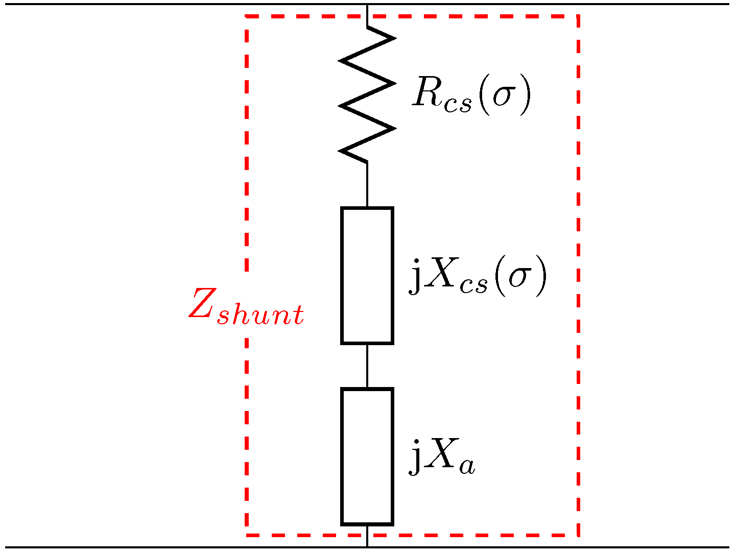
From Equation (11) and Equation (12), one finds relationship. Therefore, we can consider the strip discontinuity as a shunt element across a transmission line (see Figure 2). One can also show that . As a result, we find expressions for in some variational form.
We can re-arrange Equation (10) by taking the term out of the series, and also moving all terms with to the right-hand side:
The left-hand side of (13) can be factorized as . Following the Collin’s procedure, we arrive at form by multiplying both sides by , integrating over x, and dividing both sides by . Therefore, the total shunt impedance is calculated as:
By direct comparison with the analytic case solved by Collin, we can identify the terms corresponding to the equivalent circuit proposed in Figure 2. Interestingly, the second term in (14) is identical to the result derived by Collin for a lossless strip inside a waveguide which is called . On the other hand, is the contribution due to the material properties of the conductive strip ( and refer to the real and imaginary parts of ). Thus,
where
It should be noted that, for a waveguide with lossless walls, is pure imaginary while with are pure real numbers. This is due to the fact that the driving frequency f is chosen so that it is only above the cut-off frequency of the first mode and below the cut-off frequencies of all higher order modes. As a result, we see that is always pure imaginary. On the other hand, is a complex number in general, due to complex conductivity of the conductive strip.
3. Current Distribution on the Strip
The formulations for and in Equation (16) and Equation (17) are in the variational forms. This implies that choosing a testing function for does not make a huge influence on the results. Choosing an appropriate testing function, which is closer to the true current distribution, would undoubtedly improve the accuracy of the results. Nevertheless, trying different testing functions also assists with examining the numerical sensitivity to the choice of the testing functions.
3.1. Uniform Current
If the strip is reasonably thin , a rough approximation is to assume as uniform over the strip [29]
Collin also simplifies (18) for the case when the strip is exactly in the middle of the waveguide ()
Similarly, we also find expressions for :
and, for the case of the centered strip, we have:
3.2. Hyperbolic Cosine Distribution
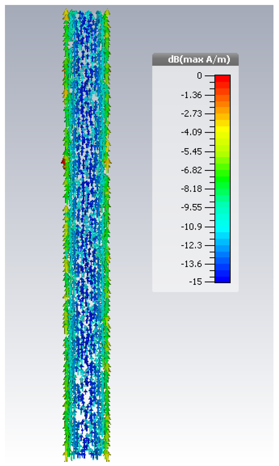
A second current distribution of was also studied for this problem. The motivation for such choice of testing function is to analytically model the singularity on the fields, especially component on the edges of the strip (). This effect significantly increases near the edges (see Figure 3 for currents on a PEC strip). By the assumption on the current as hyper cosine distribution, we get the and as
where
b is the scaling factor in the cosh basis function, and A, B and are:
It should be noted that is found by setting in (25).
4. Field on the Conductive Strip
It is instrumental to study the and fields on the discontinuity since they provide deeper insights into the problem. One can also check whether appropriate boundary conditions (here SIBC) were satisfied or not.
In the previous section, we have assumed that induced current is in the form of or where is a complex number. One finds from (11) after computing the LHS from the results of Section 3. The scattered field is then found by using (3):
where is in the following form for uniform and cosh distributions, respectively:
5. Numerical Results
Intuitive tests can be readily performed to validate the rationality of results. If the strip is assumed as PEC, then , Therefore, Equation (14) would also reduces to Equation (17). On the other hand, goes to infinity if we presume that the strip in the waveguide aperture has very low conductivity (). This is equivalent to replacing with an open circuit in the equivalent circuit (see Figure 2). Therefore, no reflections occur at zero conductivity, which resembles no discontinuity on the aperture.
To show the competency of the method, we compare our analytic method with modelling results. A general purpose programming tool [32] was used to find analytic results from Equations (18) and (22) or Equations (23) and (24). We used two commercial electromagnetic packages with a finite element method (FEM) solver [33] and method of moments (MoM) solver [34] to simulate the structures. Two different values are chosen for the complex conductivity of the strips as and which are chosen close to conductivity of the graphene at X-band.
5.1. Reflection and Transmission Coefficients
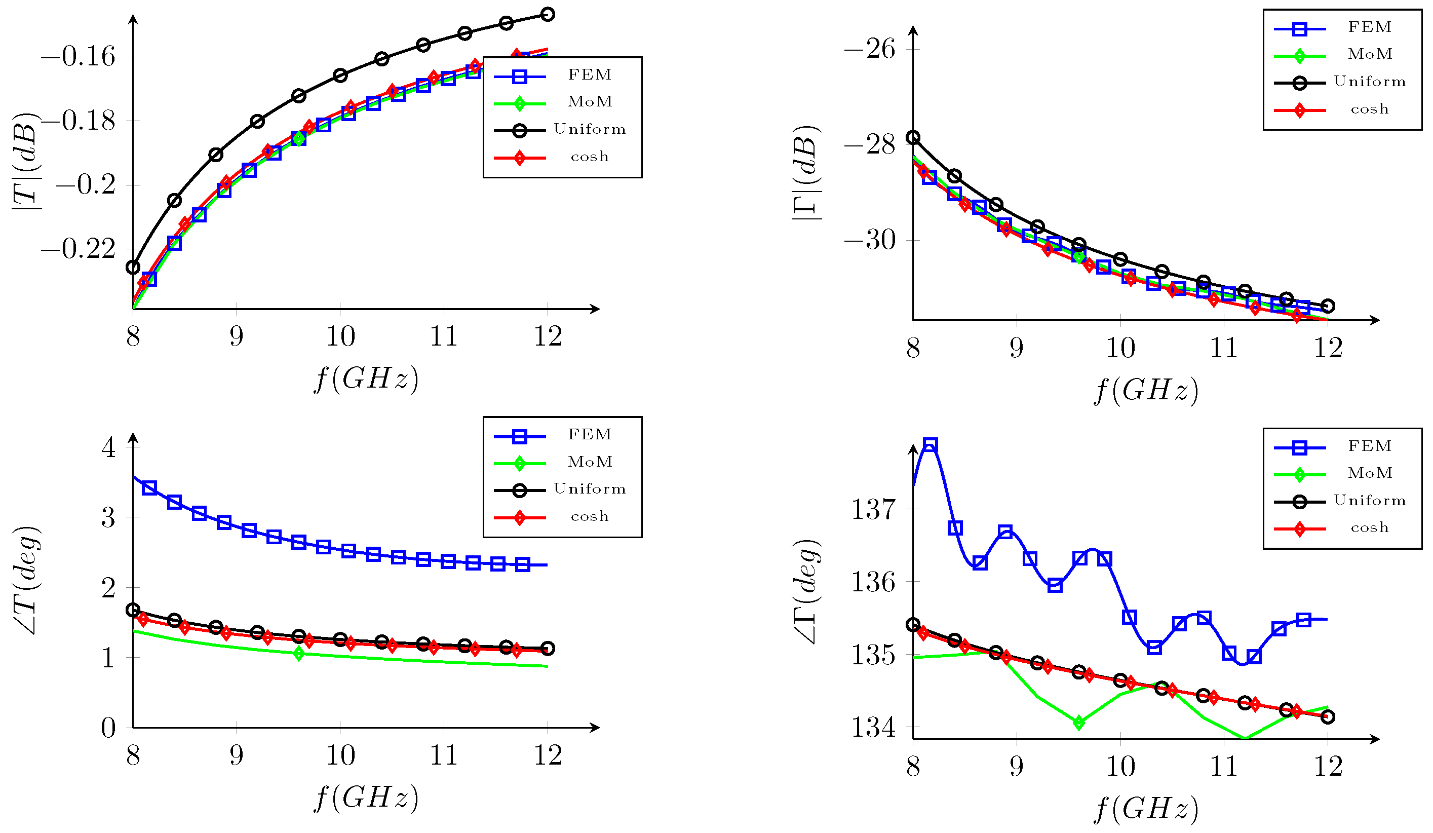
Figure 4 and Figure 5 illustrate the magnitude and phase of the reflection and transmission coefficients caused by the conductive strip discontinuity. In the modelling, we de-embedded the excitation ports to the plane of the discontinuity, in order to achieve the correct phase for and T.
A good agreement between analytic and simulation results are obtained for both current distribution (see Figure 4 and Figure 5). However, it is evident that the and T from cosh assumption are much closer to full wave modelling results. This is best illustrated on the magnitude of T and coefficients. It is also observed that MoM simulations lie closer to the theoretical calculations.
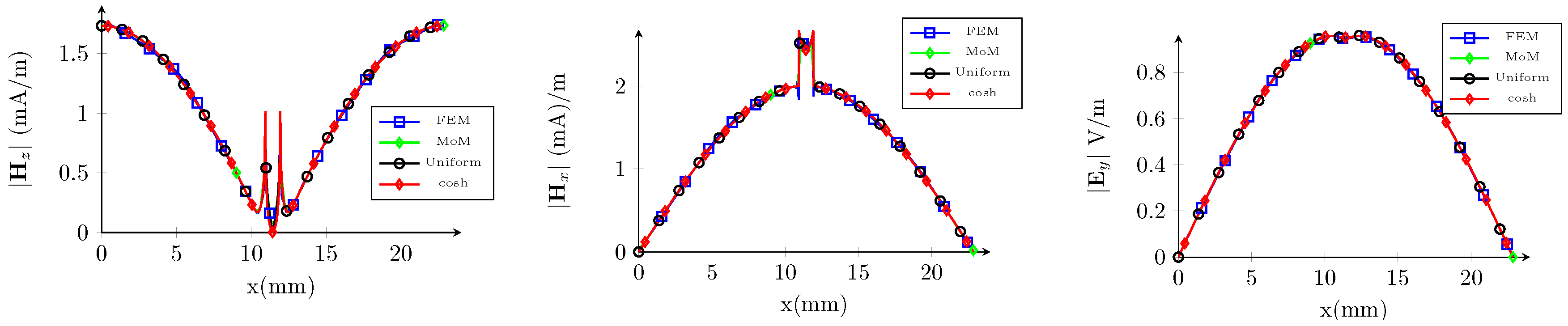
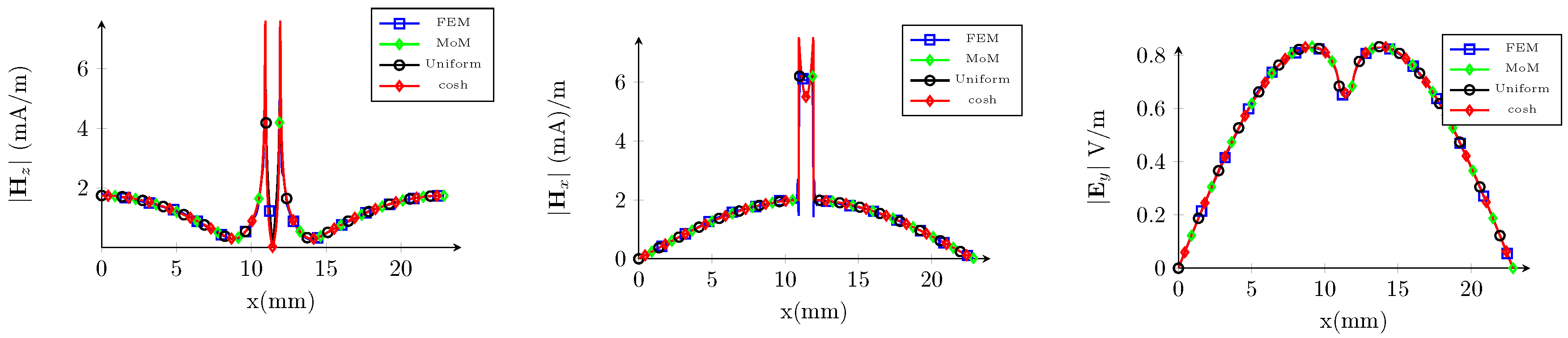
5.2. Fields on the Aperture
A perture fields on the strip discontinuity are examined in this subsection. Fields depicted in Figure 6 and Figure 7 are the total fields (incident+scattered) for a strip with 1 width. The frequency is set to 10 . The fields from both current approximations are close to the simulation results when . Particularly, and components by our approximations and full-wave solver are almost identical even on the conductive strip. component by cosh approximation disagrees slightly with results from other methods that are due to the choice of the basis function; although such a disagreement is only observed on the conductive strip and everywhere else, they are in total agreement. The singular like behaviour of the near the edges of the strip is to make a closed loop of H field around the strip (also see Figure 3).
It is interesting to see that there is a drop in and a significant jump in field to satisfy the imposed boundary conditions. To understand this phenomena, we start by recalling that the ratio of and at distances far from the discontinuity is set by the characteristic impedance of the waveguide . For a WR90 waveguide at 10 , is around 499 . However, the conductivity of the strip dictates the ratios of the transverse components of and by enforcing (6). In Figure 6 and Figure 7, is and , respectively. Therefore, comparing Figure 7 with Figure 6, a significant drop in and also a larger jump in are needed to satisfy the boundary conditions in Figure 7.
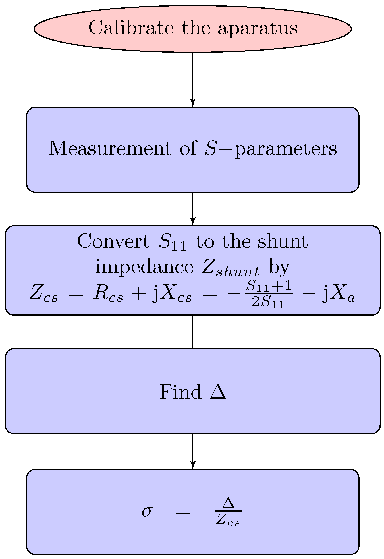
5.3. Conductivity Estimation
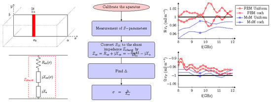
In the following, we demonstrate how one can use the analytic results of Section 3 to measure the real and imaginary part of the conductivity of a thin strip. The measurement apparatus should basically include a vector network analyser and waveguides. The diagram in Figure 8 shows the required steps in a typical apparatus. For the uniform current approximation, is found from
while , for cosh distribution, is:
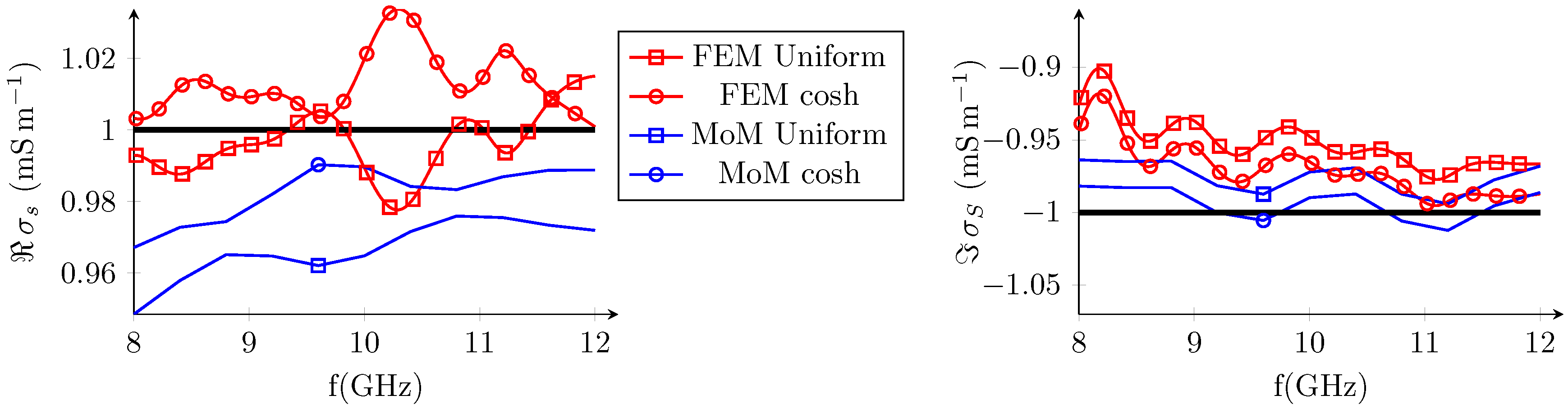
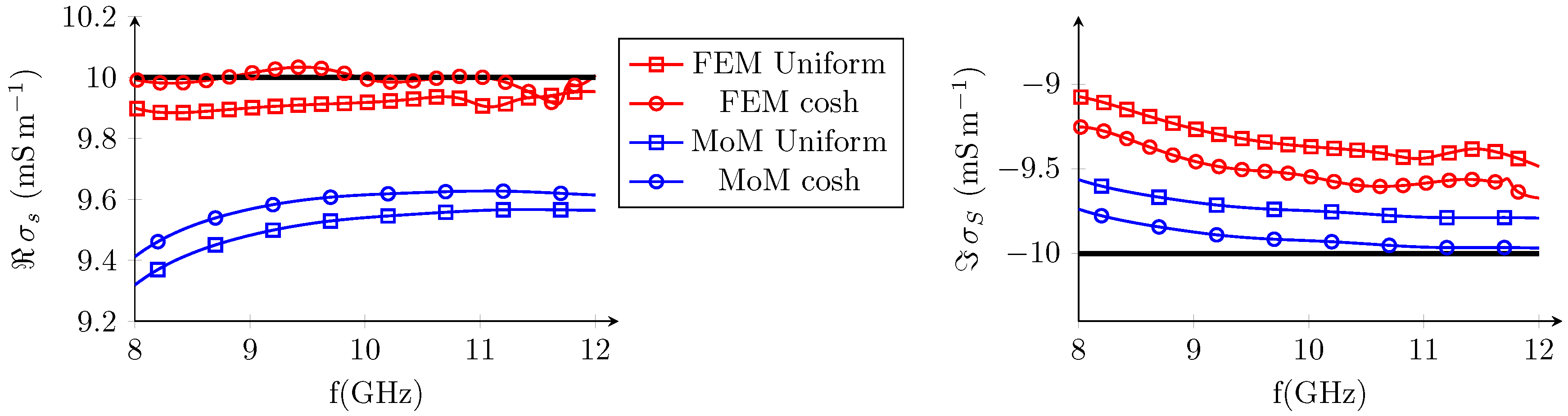
We used the modelling results of the full-wave simulators (FEM and MoM) as the input to examine the measurement procedure. S-parameters from the modelling packages are fed into the Matlab®code to estimate the values of the conductivity based on the presented theory with uniform and cosh approximations. Figure 9 and Figure 10 illustrate the computed conductivity by our method for a conductive strip of and , respectively.
Generally, the theory presented in this paper is valid for the various positions of the conductive strip inside the waveguide and along its long side. When the strip is placed at the center of the guide, the maximum reflection from the strip occurs. The interaction with the fundamental mode is stronger with the conductive strip in the middle, which improves the dynamic range of the measurement method. Further investigations are needed to explore the accuracy and sensitivity of this method to various parameters in the apparatus.
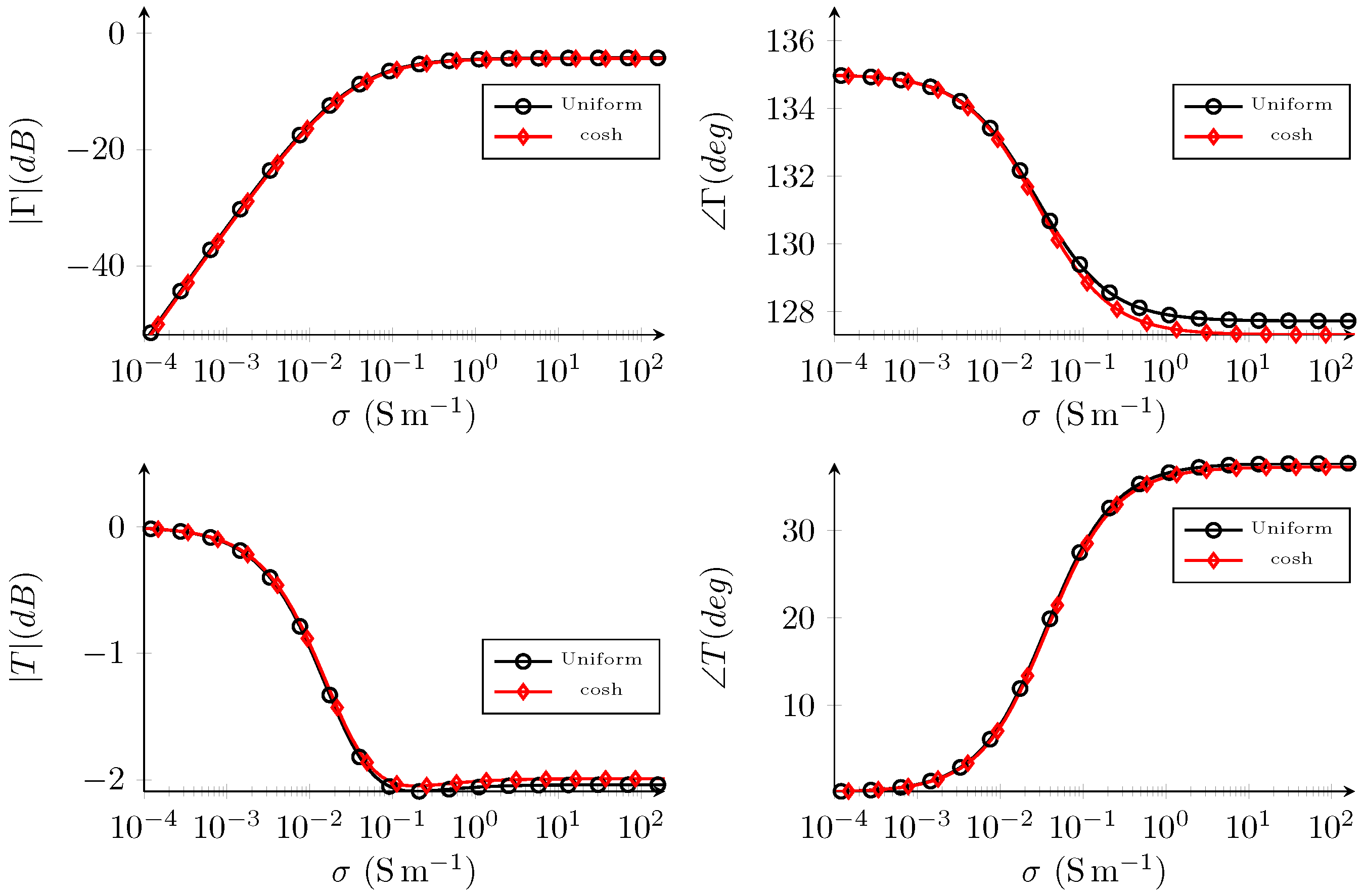
To examine the method, conductivity of a material with is swept over a range of 0.0001 to 10,000 . Reflection and transmission coefficients are plotted in Figure 11 at 10 for a strip with a width of 1 , which is placed at the centre of the waveguide. Both and T change reasonably as long as the . On the other hand, they have minimal changes if the surface conductivity is out of the specified range (it is hard to measure the dB with current status quo). This method would be most instrumental to measure the surface conductivity of the materials in the above range.
6. Conclusions
In this paper, a method to measure the conductivity of thin layers is proposed which is based on the reflection and transmission of the modes in a rectangular waveguide. Other transmission–reflection methods need sample under test to cover the aperture of the waveguide; however, our method needs SUT to only cover a small portion of the cross section. An equivalent circuit of the problem is proposed which is of assistance for intuitive understanding. We provide analytic formulas for the reflection and transmission T coefficients, and derive terms related to each component in the equivalent circuit. Distribution of the fields and currents over the SUT are also reported. The reflection and transmission coefficients from a resistive sheet are compared with S-parameters from the commercial software with FEM and MoM solvers. A reasonable agreement is observed for and T coefficients, as well as fields and currents over the aperture.
Funding
This work was partly supported by the Australian Research Council grant DP130102098.
Acknowledgments
The author is grateful to Prof. David Thiel of Griffith University for pointing out this problem as well as fruitful discussions. The manuscript was also greatly benefited by suggestions of Trevor Bird of Antengenuity, as well as his simplified closed form formula for . Finally, the author thanks Mohammad Albooyeh of UC Irvine and Dr. Mehdi Sadatgol of MTU Houghton for quickly reviewing a draft of the manuscript.
Conflicts of Interest
The author declares no conflict of interest.
Appendix A. The Simplification of Series in Equation (21)
In Equation (21), we have a series in the form of:
where . This series can be slow to converge under some conditions and it is useful to obtain a closed form solution. It is recognized that this series is the difference of two infinite series containing all terms. Thus:
where is:
The second series is looked up from the tables ([36], Section 1.443) with a change of variable of with a restriction of :
Therefore:
References
- Baker-Jarvis, J. Transmission/Reflection and Short-Circuit Line Permittivity Measurements; Technical Report, NIST Technical Note 1341; National Institute of Standards and Technology: Boulder, CO, USA, 1990.
- Chen, L.F.; Ong, C.K.; Neo, C.P.; Varadan, V.V.; Varadan, V.K. Microwave Electronics: Measurement and Materials Characterization; John Wiley Sons: Hoboken, NJ, USA, 2004. [Google Scholar]
- Kobayashi, Y.; Katoh, M. Microwave Measurement of Dielectric Properties of Low-Loss Materials by the Dielectric Rod Resonator Method. IEEE Trans. Microw. Theory Tech. 1985, 33, 586–592. [Google Scholar] [CrossRef]
- Champlin, K.S.; Krongard, R.R. The Measurement of Conductivity and Permittivity of Semiconductor Spheres by an Extension of the Cavity Perturbation Method. IRE Trans. Microw. Theory Tech. 1961, MTT-9, 545–551. [Google Scholar] [CrossRef]
- Courtney, W. Analysis and Evaluation of a Method of Measuring the Complex Permittivity and Permeability Microwave Insulators. IEEE Trans. Microw. Theory Tech. 1970, 18, 476–485. [Google Scholar] [CrossRef]
- Krupka, J.; Judek, J.; Jastrzȩbski, C.; Ciuk, T.; Wosik, J.; Zdrojek, M. Microwave complex conductivity of the YBCO thin films as a function of static external magnetic field. Appl. Phys. Lett. 2014, 104, 102603. [Google Scholar] [CrossRef]
- Le Floch, J.M.; Fan, Y.; Humbert, G.; Shan, Q.; Férachou, D.; Bara-Maillet, R.; Aubourg, M.; Hartnett, J.G.; Madrangeas, V.; Cros, D.; et al. Invited article: Dielectric material characterization techniques and designs of high-Q resonators for applications from micro to millimeter-waves frequencies applicable at room and cryogenic temperatures. Rev. Sci. Instrum. 2014, 85, 031301. [Google Scholar] [CrossRef] [PubMed]
- Krupka, J.; Strupinski, W.; Kwietniewski, N. Microwave Conductivity of Very Thin Graphene and Metal Films. J. Nanosci. Nanotechnol. 2011, 11, 3358–3362. [Google Scholar] [CrossRef] [PubMed]
- Hao, L.; Gallop, J.; Goniszewski, S.; Shaforost, O.; Klein, N.; Yakimova, R. Non-contact method for measurement of the microwave conductivity of graphene. Appl. Phys. Lett. 2013, 103, 123103. [Google Scholar] [CrossRef] [Green Version]
- Ilić, A.Ž.; Budimir, D. Electromagnetic analysis of graphene based tunable waveguide resonators. Microw. Opt. Technol. Lett. 2014, 56, 2385–2388. [Google Scholar] [CrossRef]
- Obrzut, J.; Emiroglu, C.; Kirillov, O.; Yang, Y.; Elmquist, R.E. Surface conductance of graphene from non-contact resonant cavity. Measurement 2016, 87, 146–151. [Google Scholar] [CrossRef] [Green Version]
- Kato, Y.; Horibe, M. New Permittivity Measurement Methods Using Resonant Phenomena for High-Permittivity Materials. IEEE Trans. Instrum. Meas. 2017, 66, 1191–1200. [Google Scholar] [CrossRef]
- Nozaki, R.; Bose, T. Broadband complex permittivity measurements by time-domain spectroscopy. IEEE Trans. Instrum. Meas. 1990, 39, 945–951. [Google Scholar] [CrossRef]
- Booth, J.C.; Wu, D.H.; Anlage, S.M. A broadband method for the measurement of the surface impedance of thin films at microwave frequencies. Rev. Sci. Instrum. 1994, 65, 2082–2090. [Google Scholar] [CrossRef]
- Rzepecka, M.A.; Stuchly, S.S. A Lumped Capacitance Method for the Measurement of the Permittivity and Conductivity in the Frequency and Time Domain-A Further Analysis. IEEE Trans. Instrum. Meas. 1975, 24, 27–32. [Google Scholar] [CrossRef]
- Nag, B.; Roy, S.; Chatterji, C. Microwave measurement of conductivity and dielectric constant of semiconductors. Proc. IEEE 1963, 51, 962. [Google Scholar] [CrossRef]
- Abdulnour, J.; Akyel, C.; Wu, K. A generic approach for permittivity measurement of dielectric materials using a discontinuity in a rectangular waveguide or a microstrip line. IEEE Trans. Microw. Theory Tech. 1995, 43, 1060–1066. [Google Scholar] [CrossRef]
- Hong, Y.K.; Lee, C.Y.; Jeong, C.K.; Lee, D.E.; Kim, K.; Joo, J. Method and apparatus to measure electromagnetic interference shielding efficiency and its shielding characteristics in broadband frequency ranges. Rev. Sci. Instrum. 2003, 74, 1098–1102. [Google Scholar] [CrossRef]
- Wei, X.C.; Xu, Y.L.; Meng, N.; Xu, Y.; Hakro, A.; Dai, G.L.; Hao, R.; Li, E.P. A non-contact graphene surface scattering rate characterization method at microwave frequency by combining Raman spectroscopy and coaxial connectors measurement. Carbon N. Y. 2014, 77, 53–58. [Google Scholar] [CrossRef]
- Gomez-Diaz, J.S.; Perruisseau-Carrier, J.; Sharma, P.; Ionescu, A. Non-contact characterization of graphene surface impedance at micro and millimeter waves. J. Appl. Phys. 2012, 111, 114908. [Google Scholar] [CrossRef]
- Rostamnejadi, A. Microwave properties of La0.8Ag0.2MnO3 nanoparticles. Appl. Phys. A 2016, 122, 966. [Google Scholar] [CrossRef]
- Hassan, A.M.; Obrzut, J.; Garboczi, E.J. A Q-Band Free-Space Characterization of Carbon Nanotube Composites. IEEE Trans. Microw. Theory Tech. 2016, 64, 3807–3819. [Google Scholar] [CrossRef]
- Han, J.; Geyi, W. A New Method for Measuring the Properties of Dielectric Materials. IEEE Antennas Wirel. Propag. Lett. 2013, 12, 425–428. [Google Scholar] [CrossRef]
- Jiang, J.; Geyi, W. Development of a new prototype system for measuring the permittivity of dielectric materials. J. Eng. 2014, 2014, 302–304. [Google Scholar] [CrossRef]
- Wang, X.; Geyi, W. Design of a Wideband System for Measuring Dielectric Properties. IEEE Trans. Instrum. Meas. 2017, 66, 69–76. [Google Scholar] [CrossRef]
- Bogle, A.; Havrilla, M.; Nyquis, D.; Kempel, L.; Rothwell, E. Electromagnetic Material Characterization using a Partially-Filled Rectangular Waveguide. J. Electromagn. Waves Appl. 2005, 19, 1291–1306. [Google Scholar] [CrossRef]
- Thiel, D.V.; Li, Q.; Li, X.; Gu, M. Laser induced carbon nano-structures for planar antenna fabrication at microwave frequencies. In Proceedings of the 2014 IEEE Antennas and Propagation Society International Symposium (APSURSI), Memphis, TN, USA, 6–11 July 2014; Volume 3, pp. 898–899. [Google Scholar]
- Wang, W.; Chakrabarti, S.; Chen, Z.; Yan, Z.; Tade, M.O.; Zou, J.; Li, Q. A novel bottom-up solvothermal synthesis of carbon nanosheets. J. Mater. Chem. A 2014, 2, 2390. [Google Scholar] [CrossRef]
- Collin, R.E. Field Theory of Guided Waves, 2nd ed.; IEEE-Press: Piscataway, NJ, USA, 1991. [Google Scholar]
- Senior, T.B.A.; Volakis, J.L. Approximate Boundary Conditions in Electromagnetics; No. 41; IET: London, UK, 1995. [Google Scholar]
- Bird, T.; Antengenuity, Eastwood NSW, Australia. Personal communication, 2017.
- Mathworks Inc. Available online: www.MATHWORKS.com (accessed on 6 December 2018).
- CST Microwave Studio. Available online: www.cst.com (accessed on 6 December 2018).
- FEKO. EM Software & Systems. Available online: www.feko.info (accessed on 6 December 2018).
- Kline, M. Euler and Infinite Series. Math. Mag. 1983, 56, 307–314. [Google Scholar] [CrossRef]
- Jeffrey, A.; Zwillinger, D. Table of Integrals, Series, and Products, 7th ed.; Elsevier Science: Amsterdam, The Netherlands, 2007. [Google Scholar]
Sample Availability: Matlab codes to reproduce the figures are accessible via the Code Oceans®, https://doi.org/10.24433/CO.742c3ef5-4861-4d48-92a2-b2c45c669d3d; Simulation models to verify the modelling results are available via FigShare®, https://figshare.com/s/1116824ed2b8477319d2. |
Figure 1.
Geometry of the problem; thin strip of width inside the rectangular waveguide.

Figure 2.
Equivalent circuit for a conductive strip inside waveguide.

Figure 3.
Currents on the conductive strip (x–y plane).

Figure 4.
Magnitude and phase of the reflection and transmission coefficient T from a strip with .

Figure 5.
Magnitude and phase of the reflection and transmission coefficient T from a strip with .

Figure 6.
Fields on the aperture of the waveguide and discontinuity of conductive strip. field at and H fields at with conductivity of strip set to .
Figure 6.
Fields on the aperture of the waveguide and discontinuity of conductive strip. field at and H fields at with conductivity of strip set to .

Figure 7.
Fields on the aperture of the waveguide and discontinuity of conductive strip. field at and H fields at with conductivity of strip set to .
Figure 7.
Fields on the aperture of the waveguide and discontinuity of conductive strip. field at and H fields at with conductivity of strip set to .

Figure 8.
The procedure to measure the conductivity by the proposed method.

Figure 9.
Estimated conductivity for a strip with surface conductivity of . The solid black line shows the expected value; (top) real part (bottom) imaginary part of surface conductivity.
Figure 9.
Estimated conductivity for a strip with surface conductivity of . The solid black line shows the expected value; (top) real part (bottom) imaginary part of surface conductivity.

Figure 10.
Estimated conductivity for a strip with surface conductivity of . The solid black line shows the expected value; (top) real part; (bottom) imaginary part of surface conductivity.
Figure 10.
Estimated conductivity for a strip with surface conductivity of . The solid black line shows the expected value; (top) real part; (bottom) imaginary part of surface conductivity.

Figure 11.
Variation of and T coefficients with sweeping conductivity.

© 2018 by the author. Licensee MDPI, Basel, Switzerland. This article is an open access article distributed under the terms and conditions of the Creative Commons Attribution (CC BY) license (http://creativecommons.org/licenses/by/4.0/).
Share and Cite
MDPI and ACS Style
Shahpari, M. Determination of Complex Conductivity of Thin Strips with a Transmission Method. Electronics 2019, 8, 21. https://doi.org/10.3390/electronics8010021
AMA Style
Shahpari M. Determination of Complex Conductivity of Thin Strips with a Transmission Method. Electronics. 2019; 8(1):21. https://doi.org/10.3390/electronics8010021
Chicago/Turabian StyleShahpari, Morteza. 2019. "Determination of Complex Conductivity of Thin Strips with a Transmission Method" Electronics 8, no. 1: 21. https://doi.org/10.3390/electronics8010021
Note that from the first issue of 2016, this journal uses article numbers instead of page numbers. See further details here.