A 2.5-GHz 1-V High Efficiency CMOS Power Amplifier IC with a Dual-Switching Transistor and Third Harmonic Tuning Technique


1
Department of Electrical Engineering, Universitas Indonesia, Depok 16424, Indonesia
2
Graduate School of Information, Production and Systems, Waseda University, Kitakyushu-shi 808-0135, Japan
*
Author to whom correspondence should be addressed.
Electronics 2019, 8(1), 69; https://doi.org/10.3390/electronics8010069
Submission received: 29 October 2018
/
Revised: 2 January 2019
/
Accepted: 2 January 2019
/
Published: 8 January 2019
(This article belongs to the Special Issue Nanoelectronic Materials, Devices and Modeling)
Abstract
:This paper presents a 2.5-GHz low-voltage, high-efficiency CMOS power amplifier (PA) IC in 0.18-µm CMOS technology. The combination of a dual-switching transistor (DST) and a third harmonic tuning technique is proposed. The DST effectively improves the gain at the saturation power region when the additional gain extension of the secondary switching transistor compensates for the gain compression of the primary one. To achieve high-efficiency performance, the third harmonic tuning circuit is connected in parallel to the output load. Therefore, the flattened drain current and voltage waveforms are generated, which in turn reduce the overlapping and the dc power consumption significantly. In addition, a 0.5-V back-gate voltage is applied to the primary switching transistor to realize the low-voltage operation. At 1 V of supply voltage, the proposed PA has achieved a power added efficiency (PAE) of 34.5% and a saturated output power of 10.1 dBm.
1. Introduction
For modern communication systems, such as short-range wireless applications, a high-efficiency power amplifier plays an important role in maintaining the battery life. To increase the efficiency, switching-mode amplifiers, such as class-E and class-F, are widely used [1,2,3,4]. By minimizing the overlap between the drain current and voltage waveforms, the dc power dissipation of the amplifiers can be diminished. The output power of switching-mode amplifiers is also comparable to current-mode ones for the same device peak voltage and current [5].
Unfortunately, efficiency and supply voltage represent a trade-off in switching-mode power amplifiers (PAs). Several techniques have been proposed for improving efficiency at low supply voltages [6,7,8,9,10,11]. The fully integrated PAs with a power combiner, such as multiple LC baluns [6], a transformer [7], and a distributed active transformer [8,9], were proposed to boost the power added efficiency (PAE) at low supply voltages. PAE is the ratio of the produced signal power (the difference between the output and input power) and the dc power consumption. However, large combiners lead to high insertion losses and enlarge the chip size. Another approach to increase the efficiency of a low supply voltage PA is an injection-locking technique [10,11]. Although this technique provides high gain and high efficiency, the circuit is complicated.
The harmonic manipulation techniques, such as class-J [12] and a tuned amplifier [13,14,15], are also attractive to improve efficiency. However, class-J employs only second harmonic tuning at the output port, while the tuned amplifier in [15] utilizes second and third harmonic tuning at the input and output ports. Both of the techniques increase the fundamental output power with high efficiency. The amplifier using a second harmonic short in [16] has a higher output power capability of 6.6% than the conventional class-E amplifier. However, the peak drain voltage increases significantly.
In this work, a high-efficiency CMOS PA IC operating at a low supply voltage is proposed using 0.18-µm CMOS technology. To boost the PAE, a dual-switching transistor (DST) was adopted in combination with a third harmonic tuning technique [17]. The class-E PA topology was employed as a basic structure, and 0.5-V positive, back-gate voltage was injected for low-voltage operation. A detailed theoretical and circuit analysis was performed, and the optimum circuit parameters were derived.
This paper is organized as follows. In Section 2, the circuit analysis of the proposed configuration is described, and the optimum circuit parameters are derived. Section 3 shows the simulation results of the proposed PA. Section 4 discusses the measurement results and compares them with recently reported PAs. Our conclusions are presented in Section 5.
2. Circuit Analysis
2.1. Dual-Switching Transistor (DST)
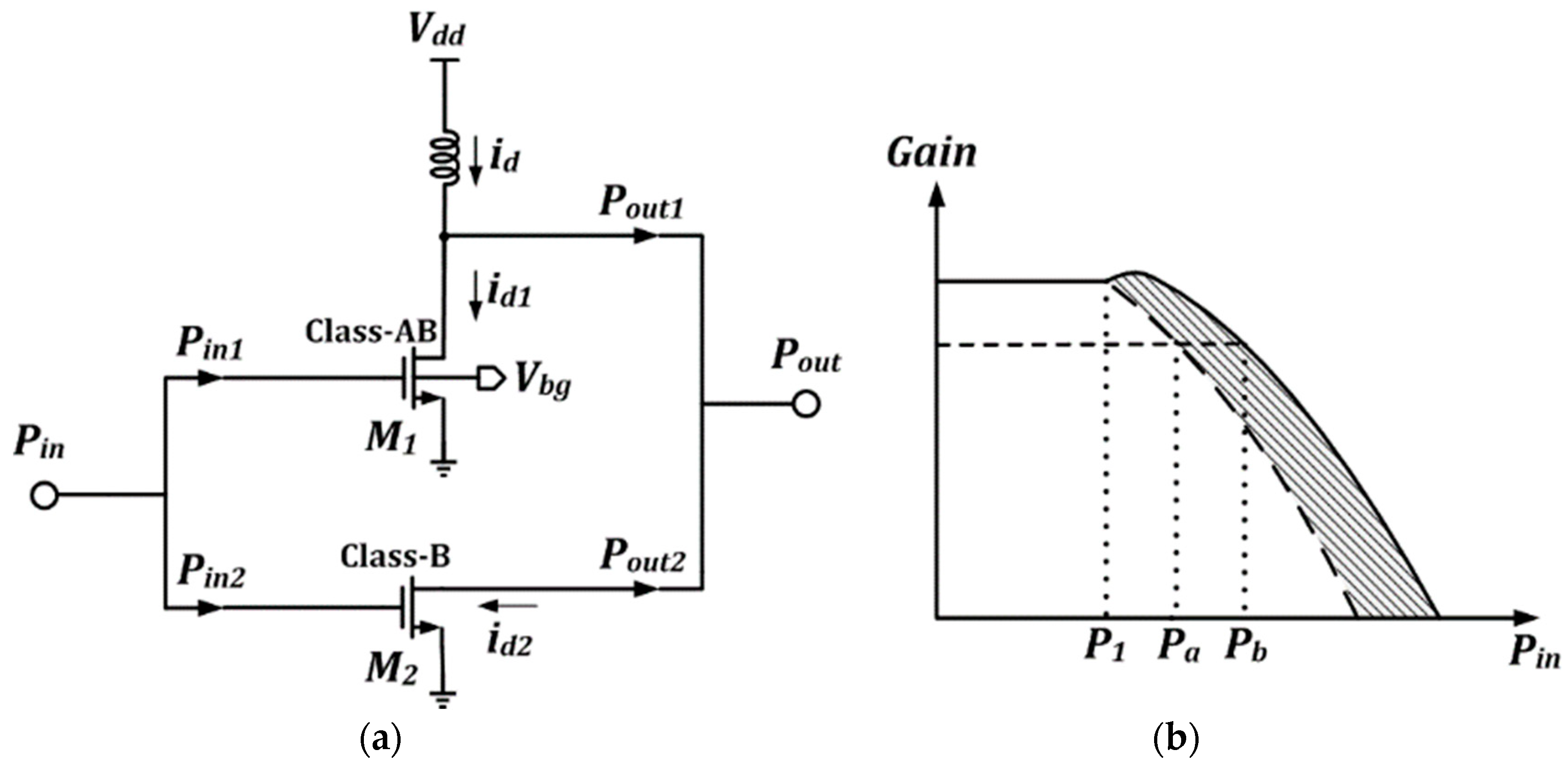
Figure 1a,b show the operation principle and the input/output characteristics of the DST structure, respectively. The structure consists of two switching transistors: (1) the primary switching transistor M1 biased at class-AB and (2) the secondary switching transistor M2 biased at class-B, which are connected in parallel. Only single input and output matching circuits were employed, thus providing less complexity for the single chip implementation. To realize the class-AB operation of M1, the positive back-gate voltage Vbg was injected. Hence, the threshold voltage decreased so that the overdrive voltage of M1 would be sufficient for the class-AB operation.
At small input power (Pin < P1), the total output power is mainly contributed by M1 (Pout = Pout1), because M1 is in active operation. In this condition, the total dissipation power PDC of the amplifier is equal to VddId1.
At large input power (Pin > P1), both of the switching transistors are active. M1 operates near the saturation power level and corresponds to its output power (Pout1 = Psat1), while M2 delivers the output power of Pout2. Therefore, the total output power of the amplifier Pout is the sum of the two transistors (Psat1 + Pout2). To maximize the PAE, the size of M2 is set to be sufficiently smaller than M1, hence the id2 << id1 and PDC is expected to be slightly higher than VddId1. The overlapping between the drain voltage and current waveforms of the DST should be minimized by adjusting the conduction angle of M2. Consequently, the PAE at the saturation power level is approximately represented as follows:
In addition, the additional gain expansion generated at the saturation power level by the DST (shaded area in Figure 1b) improves the linearity of the amplifier, Pb > Pa, where Pb is the input P1dB of the proposed amplifier and Pa is the input P1dB of the conventional class-AB amplifier.
2.2. Third Harmonic Tuning Technique
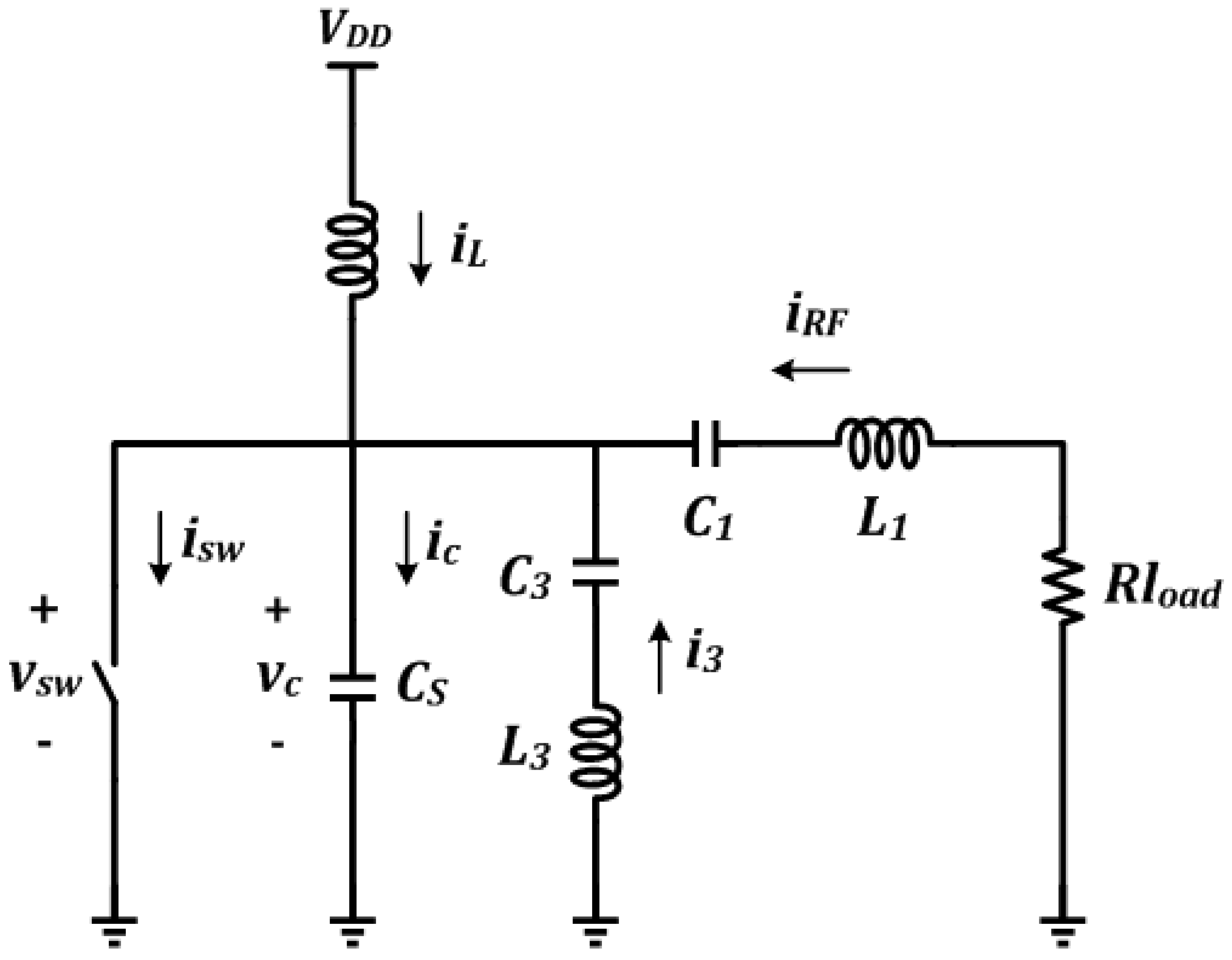
The third harmonic tuning technique shapes the voltage and current waveforms of the switching transistor at the drain node to minimize the dc power dissipation [18]. The technique is realized by connecting a series C3–L3 resonated at 3fo to the output node of the conventional class-E amplifier, as shown in Figure 2. Due to the resonator C3–L3, under specified conditions, the third harmonic component of the drain voltage and current waveforms can be controlled.
Based on a zero-voltage switching (ZVS) condition, a series of mathematical analyses was conducted to describe the operation principle of the amplifier with the third harmonic tuning circuit. The following assumptions were considered: (1) the transistor is an ideal switch, and (2) all passive elements are lossless and linear. For the operation, the transistor was driven at frequency fo and at 50% of the duty cycle (on at 0≤ ωt < π and off at π ≤ ωt <2π).
The loaded Q-factor of C1–L1 and C3–L3 were assumed to be infinite. The fundamental output current IRF and the third harmonic current I3 are represented as follows:
2.2.1. On-State Condition, 0≤ ωt < π
When the switch is turned on, the current flowing to the capacitor ic is equal to 0. Therefore, the capacitor voltage vc is equal to 0. At this interval, the current that flows to the switch isw is given by
where IL and θ denote the dc current and the initial phase angle, respectively.
Due to the characteristics of the shunt capacitor Cs, the initial current of isw during the on/off transition is zero. Hence, the following is true:
2.2.2. Off-State Condition, π ≤ ωt <2π
When the switch is turned off, isw is equal to 0. Therefore, ic can be defined as follows,
generating the voltage across the capacitor vc as,
To solve the above equations, it is assumed that the real part of the third harmonic output impedance Z3 is equal to zero. The Fourier series analyses for vc(ωt) and io(ωt) are derived to obtain the third harmonic component. Note that io(ωt) is the sum of iRF(ωt) and i3(ωt), i.e.,
The third harmonic coefficient of vc is given by
The third harmonic coefficient of io is expressed as
Substituting Equations (7)–(10), Z3 can be obtained as
Setting the real part of Z3 to zero and substituting Equation (5) for Equation (11) yields the following:
The initial phase angle (θ) can be obtained by deriving the third harmonic coefficient of isw, as follows:
At the initial condition isw (0) = 0, we have the following:
Substituting Equation (12) with Equation (14) generates the initial phase angle θ of −35°. Thus, the ratio IL/IRF of 0.57 and IL/I3 of 2.34 are obtained.
Considering that 100% efficiency is realized when the total output power is equal to the dc power consumption, the following is true:
where VDD can be defined by applying the Fourier series expansion to Equation (7), i.e.,
To realize a good switching condition, the optimum shunt capacitor Cs can be determined by substituting Equation (16) with Equation (15):
In the circuit implementation, Cs is set as the total external capacitance and output capacitance of the switching transistor.
2.2.3. Switching Waveforms
The normalized switching waveforms of drain current isw(ωt) for 0≤ ωt < π and drain voltage vc(ωt) for π ≤ ωt <2π are given by using Equations (4), (7), and (16) and the ratio of IL/IRF and IL/I3 as follows:
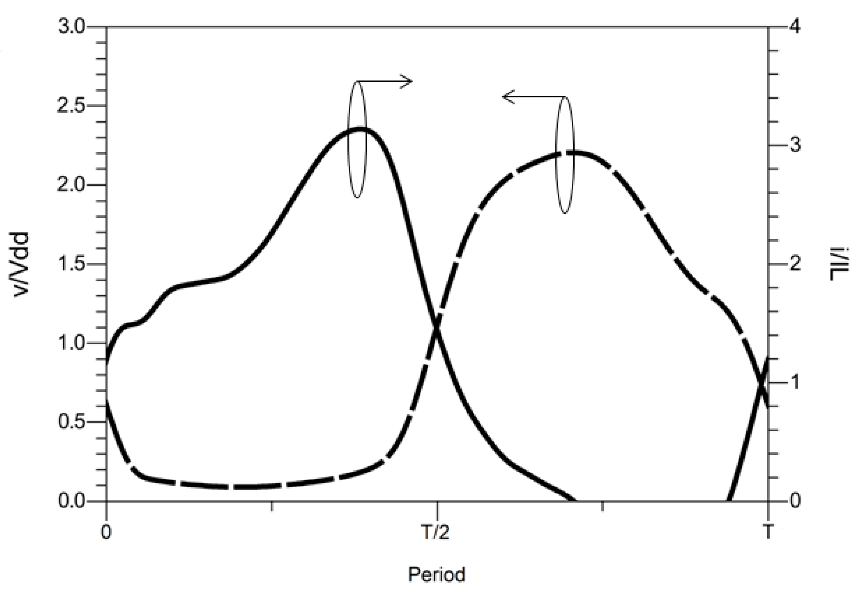
Figure 3 illustrates the normalized drain voltage (dotted line) and current waveforms (solid line) during a time period T. Because the transistor is turned on at 0≤ T < T/2, there is no voltage across the switch and the current flowing to the switch consists of dc, fundamental, and the third harmonic components. Because the transistor is turned off at T/2 ≤ T < T, all the currents flow to the shunt capacitor Cs. As shown in Figure 3, the third harmonic tuning technique flattens the waveforms and reduces the overlapping. Therefore, it is expected to achieve low dc power dissipation and high PAE. Because the technique only controls a single harmonic component at the output node, it offers a more suitable structure for single chip PA solutions than class F or class F−1.
Compared with the conventional class-E PA [19] and the second harmonic tuning PA [16], the PA with third harmonic tuning technique has a lower peak voltage waveform. The voltage stress of the switching transistor is reduced, and it is expected to get higher output power capability. For the CMOS process, the output power capability Pc calculates the maximum achievable output power for a given voltage stress Vpeak and rms drain current Irms and is expressed as follows:
The resonator C3–L3 induces a parasitic capacitance at the fundamental frequency and reduces the impedance at the output port. As a result, the loaded Q-factor of C1–L1, which is resonated at fo, is decreased. The third harmonic resonator is designed by choosing an inductor with a high Q-factor at 3fo as L3. To compromise with the overall chip area and insertion loss, the layout dimension of the inductor is optimized. Then, the series capacitance C3 is defined by the equation C3 = 1/9(πfo)2L3. The parasitic capacitance of the resonator should be minimized to maintain the optimum shunt capacitance Cs of the amplifier. Consequently, by selecting the Q-factor of 10, the third harmonic resonator is optimized to L3 = 2.5 nH and C3 =180 fF.
2.3. Back-Gate Bias Technique
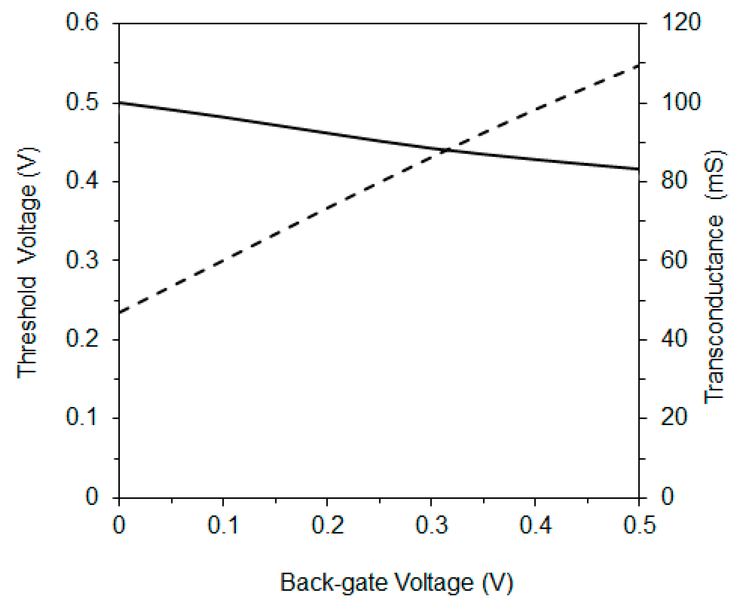
The back-gate bias technique is a method to modify the threshold voltage level and the on-resistance (Ron) of the MOSFET by connecting the body terminal to the positive or negative voltage. In this paper, a positive back-gate voltage was applied at the body of M1 so that the threshold voltage and the Ron decreased. The technique led to the p-well of the body and n+ of the source being connected in a forward bias condition. Therefore, the positive back-gate bias voltage selection is very important to minimize an excessive dc leakage current from the body to the source [20]. A solid back-gate body potential should have an ideal connection to the ground, hence a large by-pass capacitance is placed between the body and the ground. Figure 4 shows the comparison between the positive back-gate voltage versus the threshold voltage at 0.5-V bias voltage.
2.4. Circuit Configuration of the Proposed PA
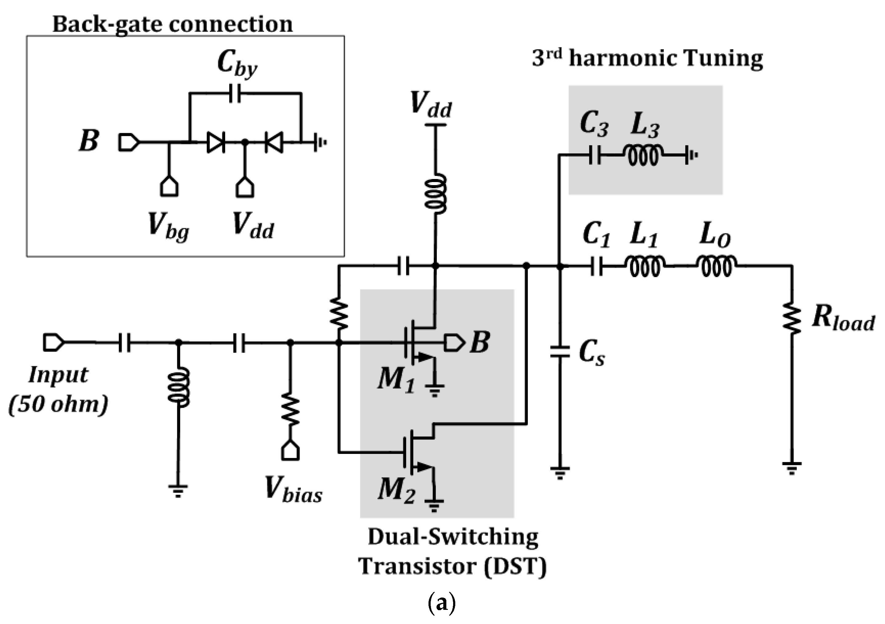
Figure 5a shows the circuit schematic of the proposed CMOS PA IC. To achieve high PAE at a low supply voltage, a combination of the DST and the third harmonic tuning circuit (C3–L3) is proposed. The supply voltage Vdd of 1 V was applied with the bias voltage Vbias of 0.5 V. In addition, a 0.5-V positive body bias was injected into the body terminal (B) of M1 by the external biasing terminal (Vbg) to decrease the threshold voltage level of 75 mV, which was optimum for the class-AB operation when there was no input power. In addition, the body of M2 was connected to the ground for the class-B operation. The RC feedback network was employed to modify the input and the output resistance for the impedance matching requirement, as well as to increase the stability of the device; hence, the PA was always unconditionally stable.
To minimize the drain loss, a large transistor size was selected. The large size, however, decreased the gain and increased the input power. In this work, the optimized total gate width of 464-µm with a gate length of 0.18-µm was utilized to obtain the power gain higher than 10 dB at 2.5-GHz. Because a large transistor size leads to high output capacitance, the shunt capacitor CS was selected by considering the total output capacitance of the DST. Furthermore, the small inductor LO was inserted at the output for impedance matching.
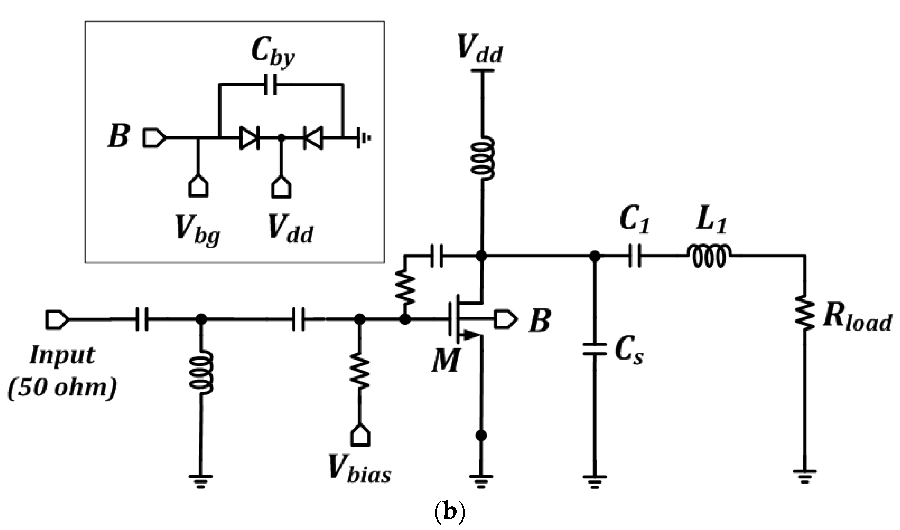
To verify the effectiveness of the proposed configuration, a 2.5-GHz conventional class-E PA was designed as illustrated in Figure 5b. The size of the switching transistor M was set equal to the total size of the switching transistors in the proposed PA. The 0.5-V back-gate voltage Vbg was injected, and the switching transistor was biased at class-AB with 1-V supply voltage
3. Simulation Results
The prototype of the proposed circuits was designed and fabricated using six metal layer (1P6M) 0.18-µm CMOS technology by TSMC. This CMOS process offered two ultra-thick top metal layers, 4-µm or 2-µm thick, for inductor implementation. High-density MIM capacitors of 1fF/µm2 and 2fF/µm2 were also provided. For noise isolation from the P-substrate, deep n-wells were available.
The small-signal and large-signal responses of the proposed PA IC were simulated on a wafer using ADS 2011 by Keysight [21] and Virtuoso ADE IC 6.1.5 by Cadence [22]. Input and output matching circuits were simulated and optimized using Momentum EM simulation in ADS 2011, while layout and verification were performed by Virtuoso ADE IC 6.1.5, respectively.
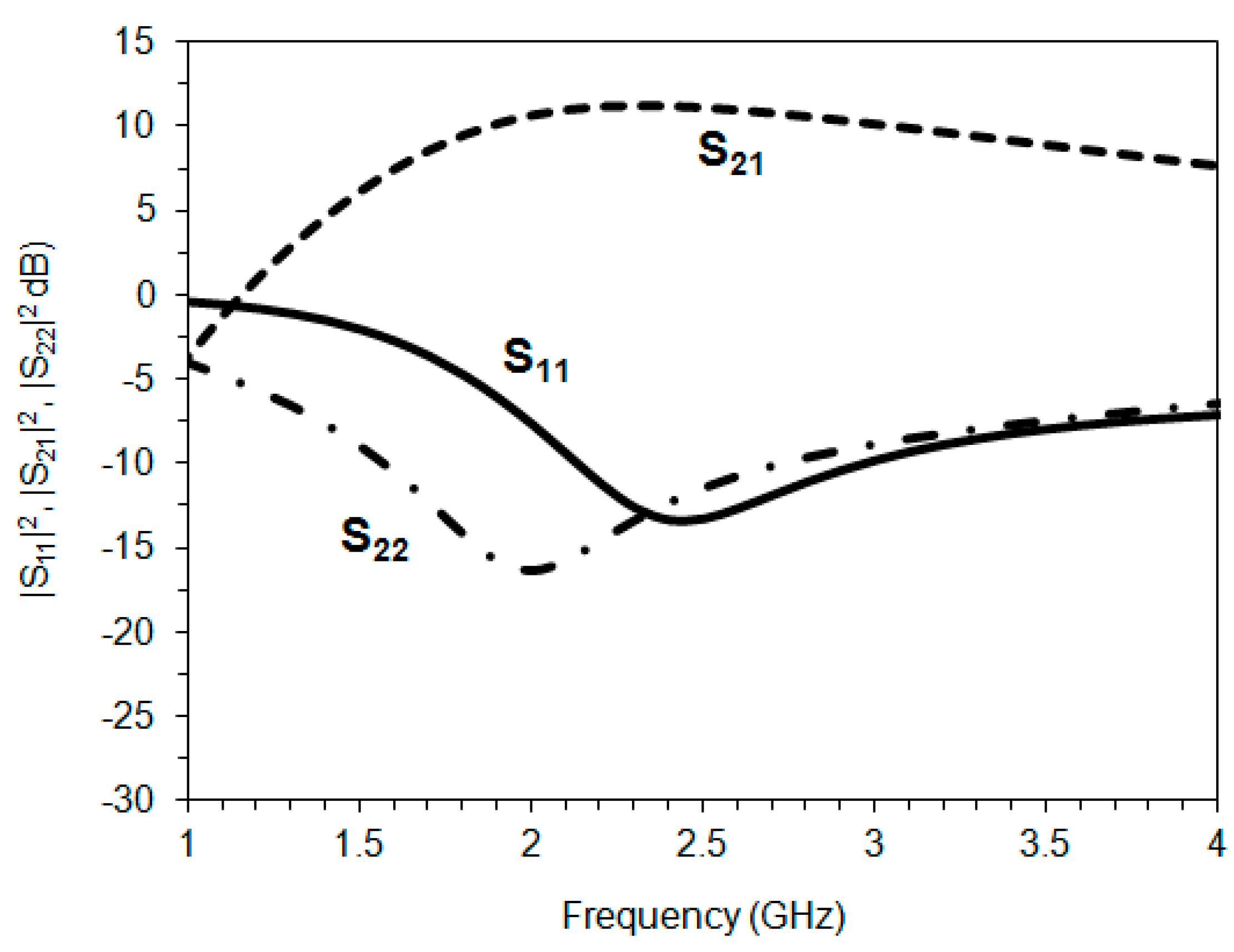
Figure 6 illustrates the small-signal input–output response of the proposed PA IC. The S11 and the S22 are −13.9 dB and −12.5 dB at 2.5 GHz, respectively. The maximum S21 is 11.2 dB with a 3-dB bandwidth from 1.65 GHz to 3.8 GHz.
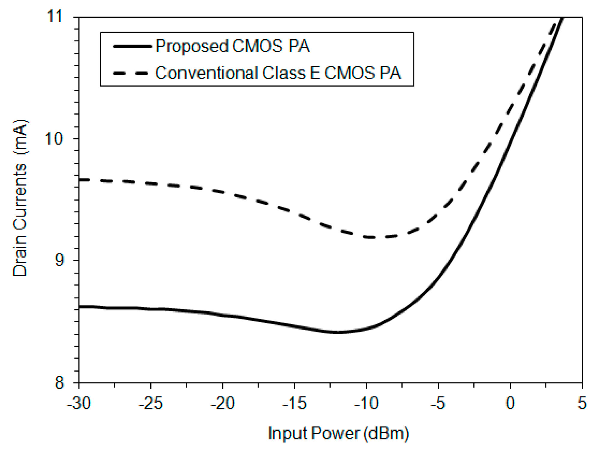
Because the third harmonic tuning technique was very effective to decrease the dc power consumption, it is expected that the proposed CMOS PA has high efficiency. Figure 7 shows the simulated dc drain current of the proposed PA IC (solid line) and the conventional PA IC (dotted line) versus the input power. The proposed CMOS PA exhibited a lower dc current than the conventional one under small-signal conditions.
Figure 8 shows the simulated input–output response of the proposed and conventional class-E PAs with sweeping the input power. It confirmed that the proposed PA IC achieves better gain linearity with better PAE than the conventional class-E PA IC. At an input power of lower than -10 dBm, M2 was turned off and the input signal was mainly amplified by M1. When the input power increased, the output power of M2 became higher to compensate for the gain compression of M1, achieving a higher linear performance. From the simulation, it was shown that the proposed PA had a power gain of 11.5 dB, an output P1dB of 8.1 dBm, and a peak PAE of 38.5%.
4. Measurement Results
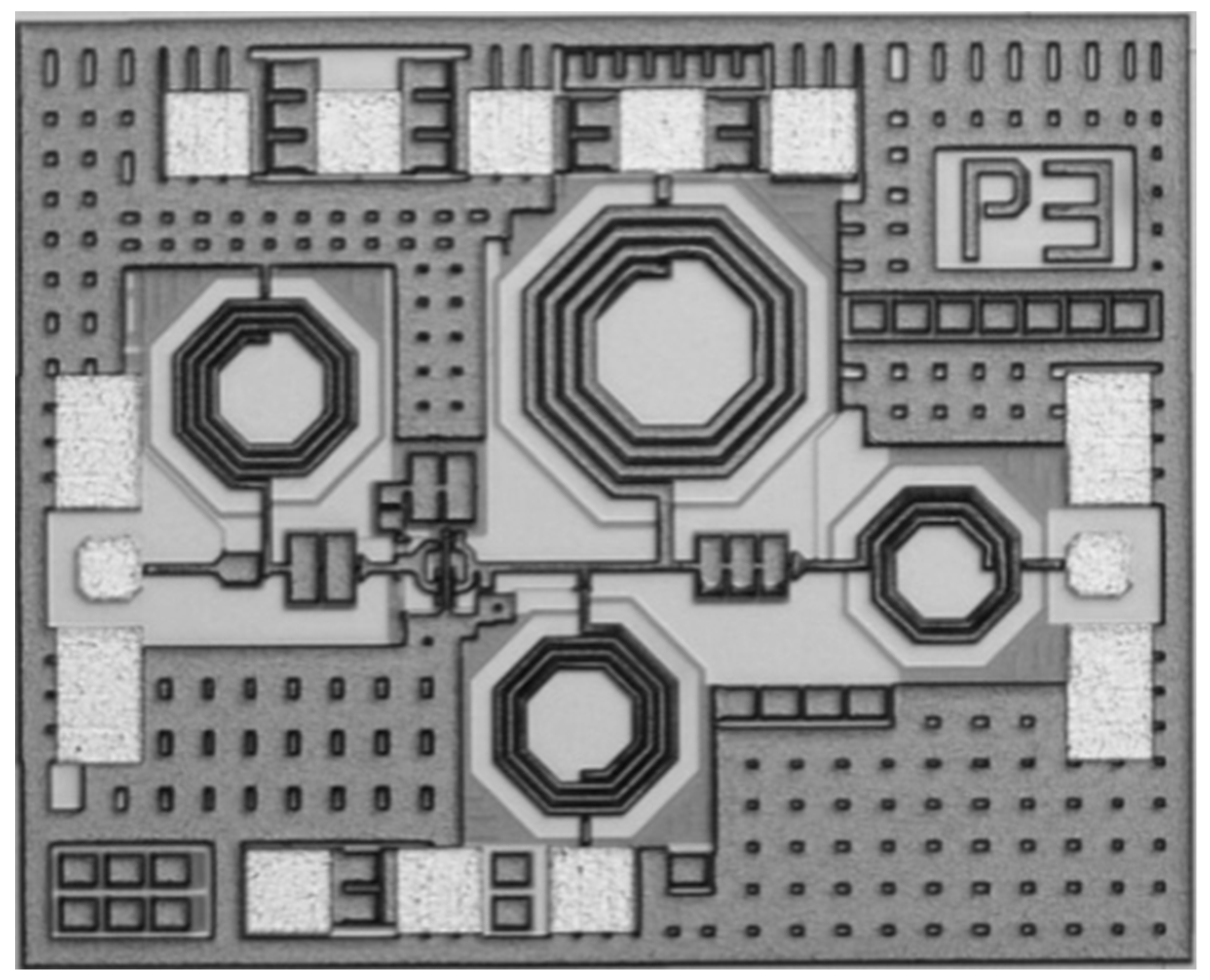
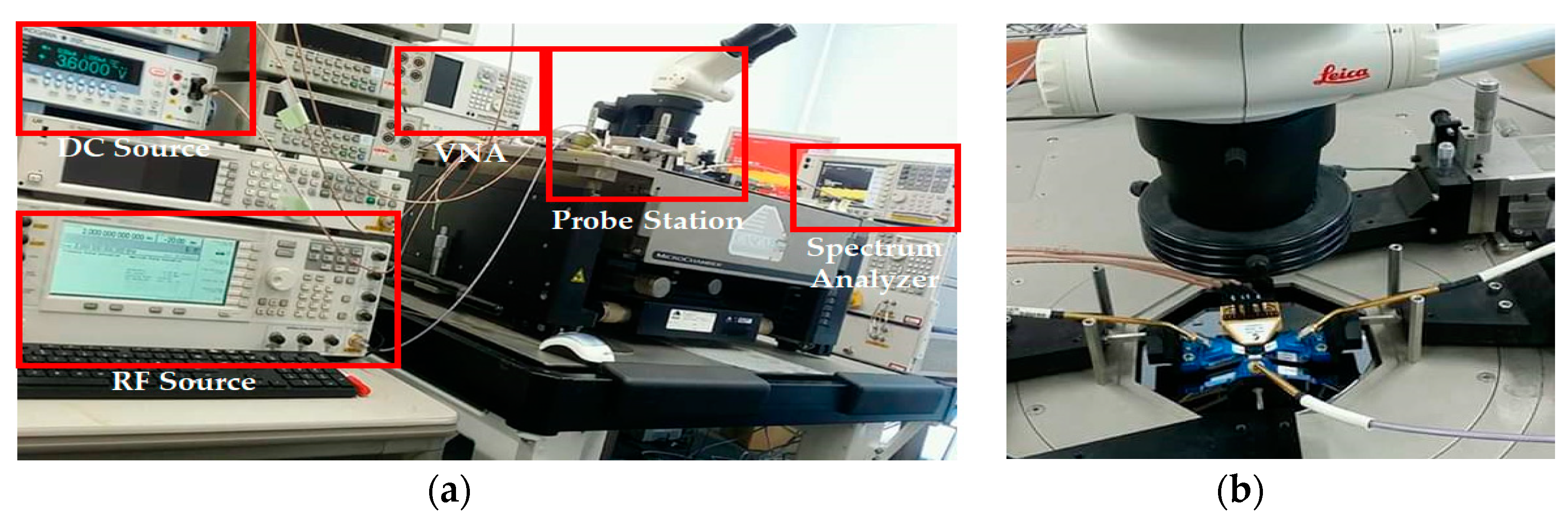
The chip photograph of the proposed PA IC is depicted in Figure 9. The proposed PA was designed in 0.18-µm CMOS technology and measured on a wafer. The chip size is 0.9-mm by 1.1-mm. Figure 10 shows the measurement setup and probing situation of the proposed CMOS PA IC. The chip was probed using Summit 11201B Cascade Microtech with a single-ended GSG probe at the input and output RF signals. The RF input was generated using an Agilent E8267D vector signal generator, while the dc source was provided by using Yokogawa GS200.
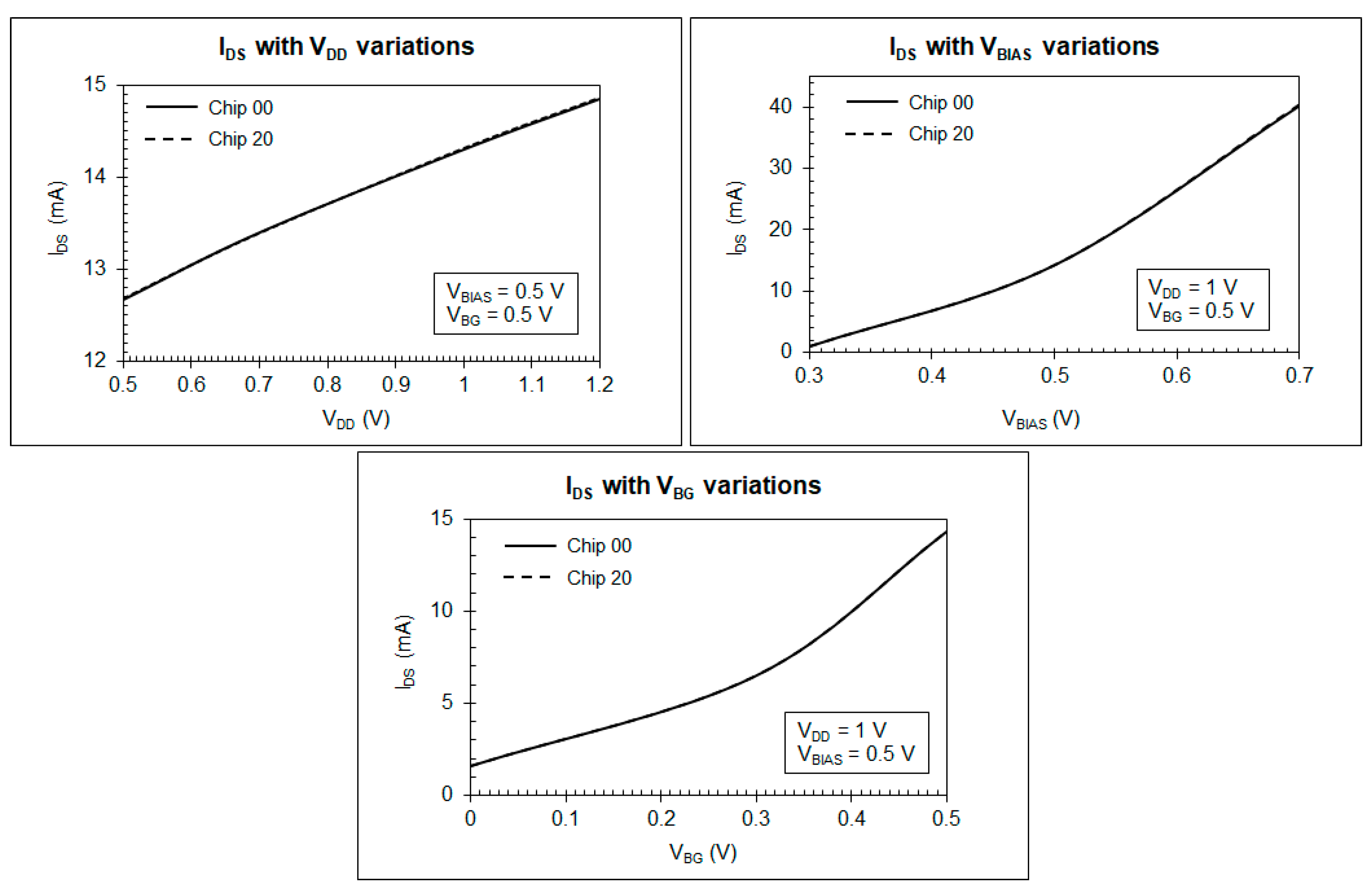
In the measurement process, 5 chips were measured for whole data variations, i.e., dc, small-signal, and large-signal performances. The average of the standard deviation of the IDS measurement was 0.03 mA, and the averages of the standard deviations of S11, S21, and S22 were 0.05 dB, 0.06 dB, and 0.1 dB, respectively. To demonstrate the uniformity performance of the PA chips, the IDS characteristics of chip 00 and chip 20 over the supply voltage (Vdd), bias voltage (Vbias), and back-gate voltage (Vbg) variations are illustrated in Figure 11.
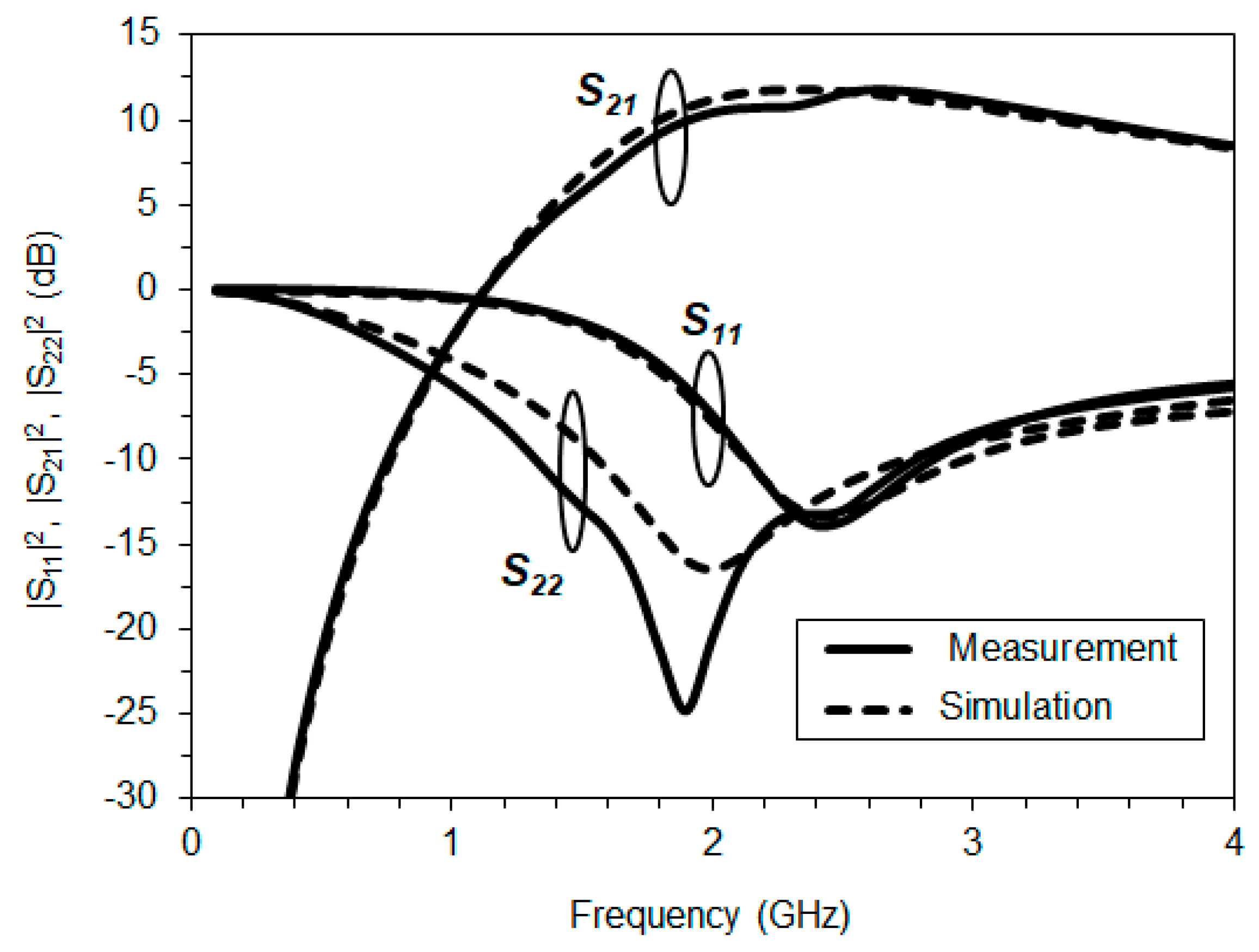
In order to demonstrate the small-signal performance based on S-parameters, the output RF was measured using the Agilent E8361A vector network analyzer. Figure 12 illustrates the comparison between the measured small-signal S-parameters (solid line) and the simulated small-signal S-parameters (dashed line) of the proposed circuits at 1 V of supply voltage. The quiescent current was 14.31 mA at 0.5 V of gate bias voltage. As expected, the measured S11 and S22 at 2.5 GHz were lower than −10 dB. The maximum small signal gain was 11.0 dB at 2.5 GHz with a 3-dB bandwidth from 1.7 GHz to 4.1 GHz. Figure 12 shows that measurement results agree well with the simulation results.
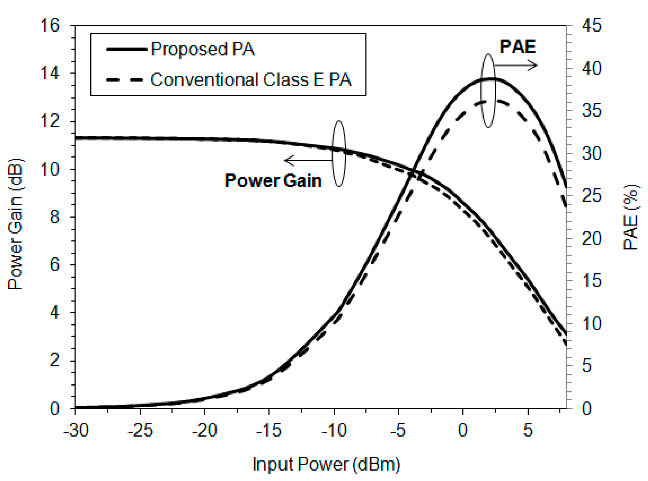
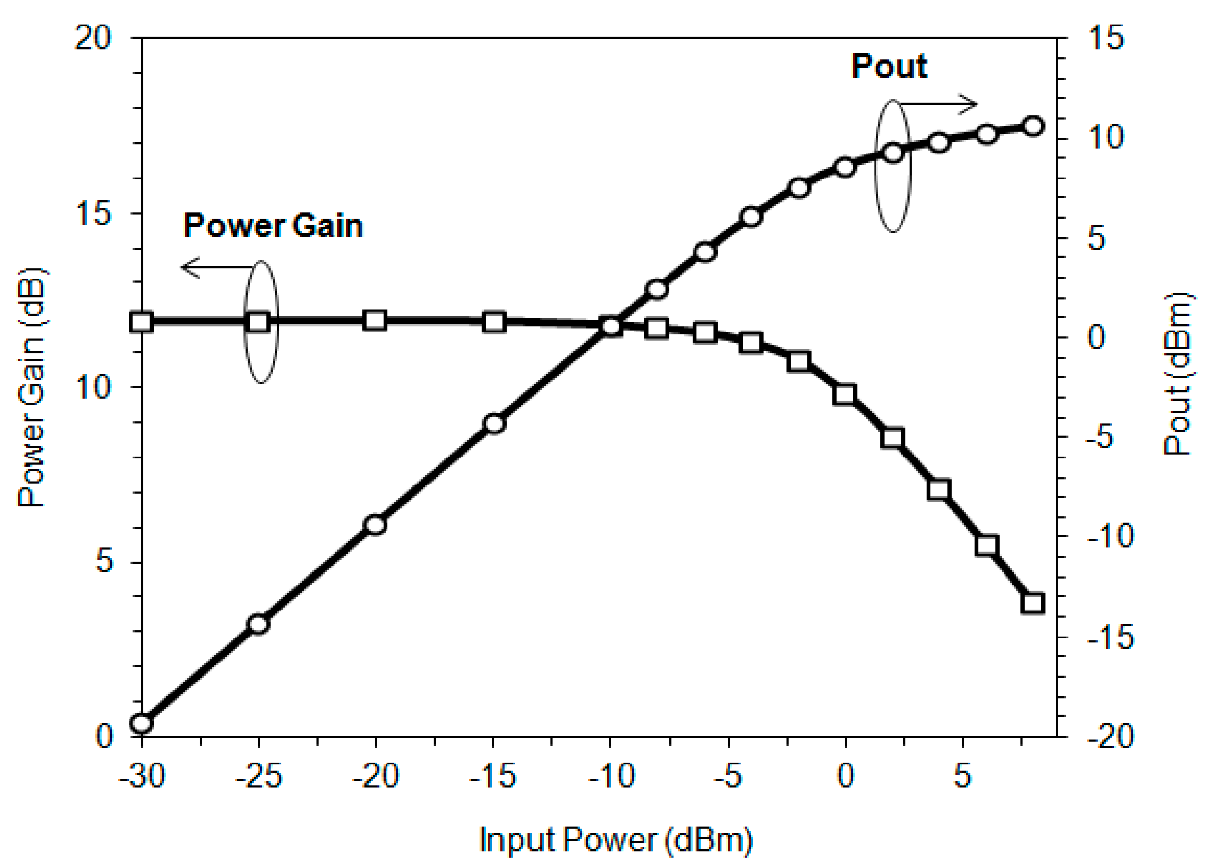
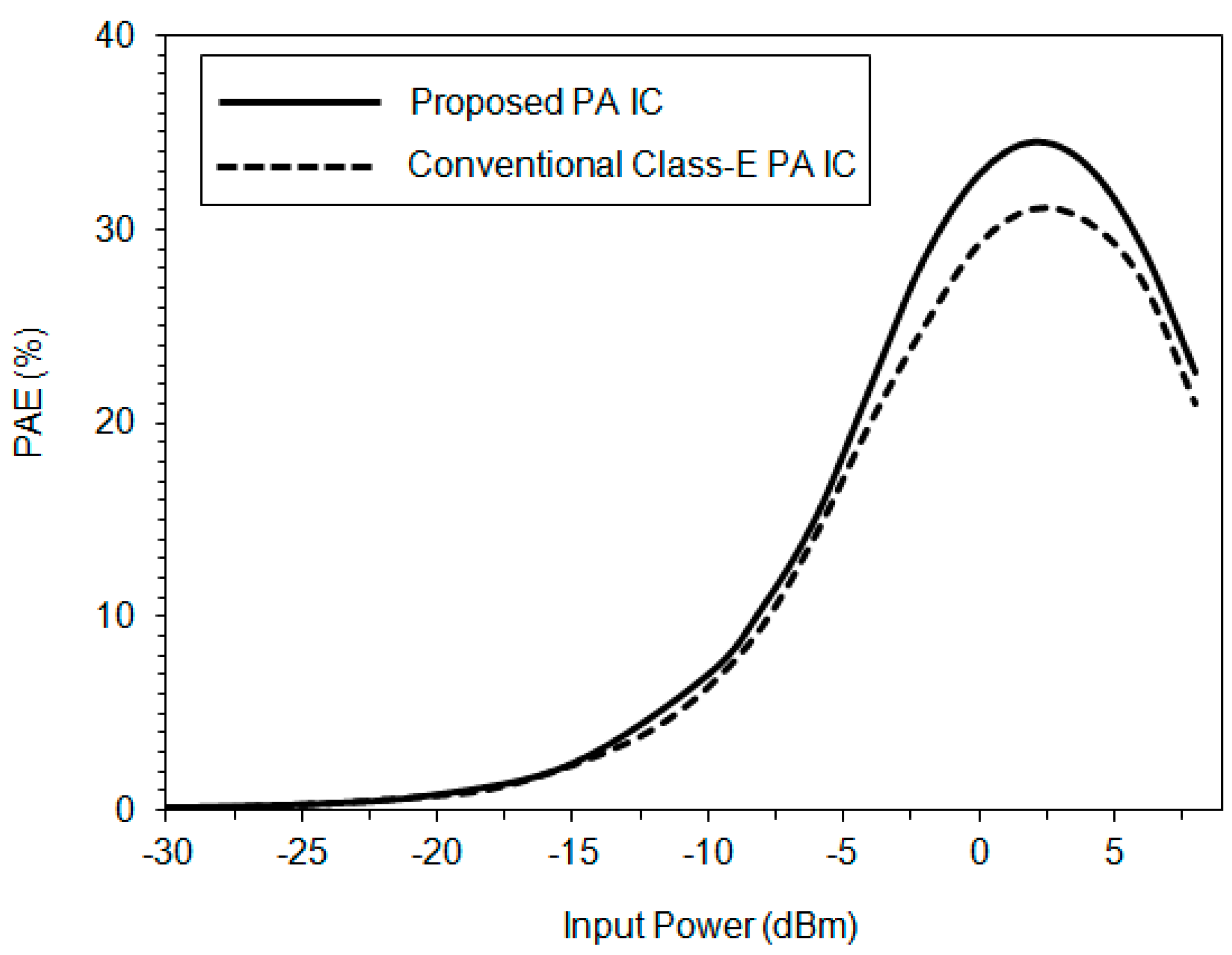
The measurement results of the power gain and the output power of the proposed CMOS PA IC are shown in Figure 13. To measure the output power, an Agilent E4448A spectrum analyzer was utilized. At a supply voltage of 1 V, the proposed PA achieved a saturated output power of 10.1 dBm and an output P1dB of 8.0 dBm. Figure 14 illustrates the measurement results of the PAE of the proposed PA (solid line) and the conventional class-E PA (dotted line) at 1 V of supply voltage. The proposed PA achieved a higher PAE than the conventional PA, with a peak PAE of 34.5%.
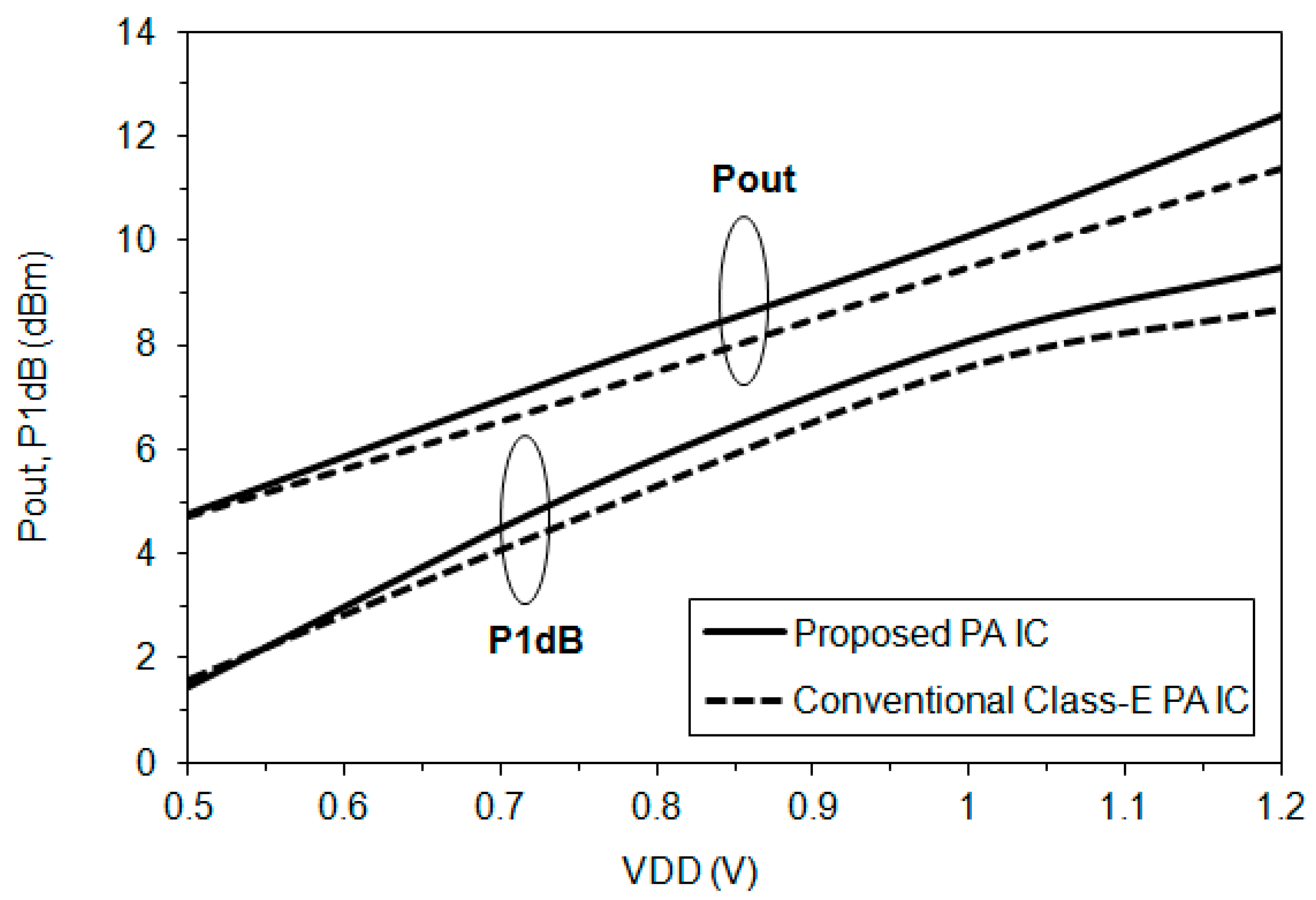
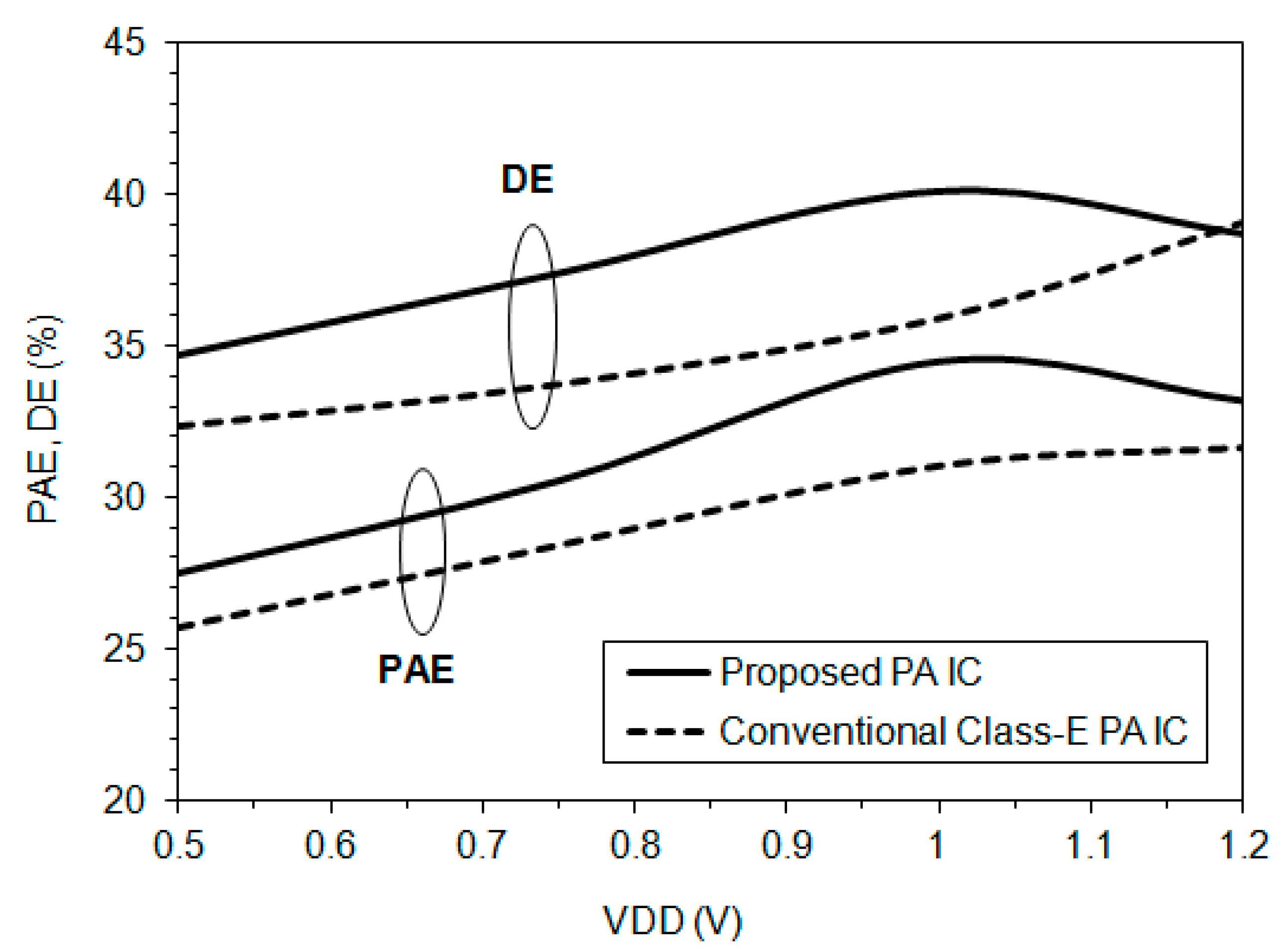
Figure 15 shows the measurement results of the output power and the P1dB of the proposed PA (solid line) and the conventional class-E PA (dotted line) versus the supply voltage variations from 0.5 V to 1.2 V. The proposed PA achieved larger saturated output power and P1dB than did the conventional PA. The dependency of the efficiency performances (drain efficiency (DE) and PAE) on the supply voltage is illustrated in Figure 16. The proposed PA achieved higher efficiency than the conventional PA at low-voltage operation. Because the load line was adjusted to obtain high efficiency at a supply voltage of 1 V, the efficiency at 1.2 V was slightly lower than that at 1 V.
Table 1 shows the performance of the proposed PA IC with several published works of low-voltage operation PAs. The proposed PA IC has achieved excellent PAE with sufficient output power at low-voltage operation compared with the previously published works.
5. Conclusions
A 2.5-GHz fully integrated CMOS PA IC has been designed and fully evaluated in 0.18-µm CMOS technology for low-voltage operation. As the input power increased, the proposed dual-switching transistor (DST) effectively improved the gain linearity with high efficiency. In addition, the third harmonic termination technique compressed the voltage waveform and modified the current waveform to realize low dc power dissipation.
At 1 V of supply voltage, the proposed CMOS PA IC exhibited a power gain of 11.0 dB, an output P1dB of 8.0 dBm, and a peak PAE of 34.5%. The measured P1dB and PAE of the proposed PA were higher than those of recently reported works. Therefore, the proposed PA IC is applicable for low-voltage operation.
Author Contributions
T.A.K. developed the idea, performed the circuit design and experiments, and wrote the initial draft. T.Y. supervised the process of this work and reviewed and revised the draft.
Funding
This work is funded by Japan Society for the Promotion of Science (JSPS) KAKENHI Grant-in-Aid for Scientific Research (B) Number 23360162. The publication process received no external funding.
Acknowledgments
This work is supported by VLSI Design and Education Center (VDEC), the University of Tokyo in collaboration with Cadence Design Systems Inc., Mentor Graphics Inc., and Keysight Technologies Japan Ltd.
Conflicts of Interest
The authors declare no conflicts of interest.
References
- Chen, P.; Yang, K.; Zhang, T. Analysis of a Class-E Power Amplifier with Shunt Filter for Any Duty Ratio. IEEE Trans. Circuits Syst. II Express Briefs 2017, 64, 857–861. [Google Scholar] [CrossRef]
- Abbasian, S.; Johnson, T. Power-Efficiency Characteristics of Class-F and Inverse Class-F Synchronous Rectifiers. IEEE Trans. Microw. Theory Tech. 2016, 64, 4740–4751. [Google Scholar] [CrossRef]
- Liu, C.; Cheng, Q.F. A Novel Compensation Circuit of High-Efficiency Concurrent Dual-Band Class-E Power Amplifiers. IEEE Microw. Wirel. Compon. Lett. 2018, 28, 720–722. [Google Scholar] [CrossRef]
- Dong, Y.; Mao, L.; Xie, S. Extended Continuous Inverse Class-F Power Amplifiers with Class-AB Bias Conditions. IEEE Microw. Wirel. Compon. Lett. 2017, 27, 368–370. [Google Scholar] [CrossRef]
- Kee, S.D.; Aoki, I.; Hajimiri, A.; Rutledge, D. The Class-E/F Family of ZVS Switching Amplifiers. IEEE Trans. Microw. Theory Tech. 2003, 51, 1677–1690. [Google Scholar] [CrossRef]
- Reynaert, P.; Steyart, M.S.J. A 2.45-GHz 0.13-um CMOS PA With Parallel Amplification. IEEE J. Solid-State Circuits 2007, 42, 551–562. [Google Scholar] [CrossRef]
- Haldi, P.; Chowdhury, D.; Reynaert, P.; Liu, G.; Niknejad, A.M. A 5.8 GHz 1 V Linier Power Amplifier Using a Novel On-Chip Transformer Power Combiner in Standard 90 nm CMOS. IEEE J. Solid-State Circuits 2008, 43, 1054–1062. [Google Scholar] [CrossRef]
- Aoki, I.; Kee, S.D.; Rutledge, D.B.; Hijimiri, A. Fully Integrated CMOS Power Amplifier Design Using the Distributed Active-Transformer Architecture. IEEE J. Solid-State Circuits 2002, 37, 371–383. [Google Scholar] [CrossRef]
- Khan, H.R.; Sajid, U.; Kanwal, S.; Zafar, F.; Wahab, Q. A Fully Integrated Distributed Active Transformer Based Power Amplifier in 0.13 um CMOS Technology. In Proceedings of the 2013 Saudi Electronics Communications and Photonics Conference (SIECPC), Fira, Greece, 27–30 April 2013. [Google Scholar] [CrossRef]
- Oh, H.S.; Song, T.; Yoon, E.; Kim, C.K. A Power-Efficient Injection-Locked Class-E Power Amplifier for Wireless Sensor Network. IEEE Microw. Wirel. Compon. Lett. 2006, 16, 173–175. [Google Scholar] [CrossRef]
- El-Desouki, M.; Deen, M.; Haddara, Y.; Marinov, O. A Fully Integrated CMOS Power Amplifier using Superharmonic Injection-Locking for Short Range Applications. IEEE Sens. J. 2011, 11, 2149–2158. [Google Scholar] [CrossRef]
- Wright, P.; Lees, J.; Benedikt, J.; Tasker, P.J.; Cripps, S.C. A Methodology for Realizing High Efficiency Class-J in a Linear and Broadband PA. IEEE Trans. Microw. Theory Tech. 2013, 57, 3196–3204. [Google Scholar] [CrossRef]
- Kusunoki, S.; Hatsugai, T. Harmonic-Injected Power Amplifier with 2nd Harmonic Short Circuit for Cellular Phones. IEICE Trans. Electron. 2005, E88-C, 729–738. [Google Scholar] [CrossRef]
- Bae, K.-T.; Lee, I.-J.; Kang, B.; Sim, S.; Jeon, L.; Kim, D.-W. X-Band GaN Power Amplifier MMIC with a Third Harmonic-Tuned Circuit. Electronics 2017, 6, 103. [Google Scholar] [CrossRef]
- Colantonio, P.; Giannini, F.; Leuzzi, G.; Limiti, E. Multiharmonic Manipulation for Highly Efficient Microwave Power Amplifier. Int. J. RF Microw. Comput. Aided Eng. 2001, 11, 366–384. [Google Scholar] [CrossRef]
- You, F.; He, S.; Tang, X.; Deng, X. High-Efficiency Single-Ended Class-E/F2 Power Amplifier with Finite DC Feed Inductor. IEEE Trans. Microw. Theory Tech. 2010, 58, 32–40. [Google Scholar] [CrossRef]
- Kurniawan, T.A.; Yang, X.; Xu, X.; Yoshimasu, T. A 2.5-GHz Band Low Voltage High Efficiency CMOS Power Amplifier IC Using Parallel Switching Transistor for Short Range Wireless Applications. In Proceedings of the 45th European Microwave Conference 2015, Paris, France, 6–11 September 2015. [Google Scholar] [CrossRef]
- Kurniawan, T.A.; Yang, X.; Xu, X.; Itoh, N.; Yoshimasu, T. A 2.5-GHz Band, 0.75-V High Efficiency CMOS Power Amplifier IC With Third Harmonic Termination Technique in 0.18-um CMOS. In Proceedings of the 2015 IEEE Wireless and Microwave Technology Conference (WAMICON), Cocoa Beach, FL, USA, 12–15 April 2015. [Google Scholar] [CrossRef]
- Grebenikov, A.; Sokal, N.O. Switch Mode RF Power Amplifiers; Newnes: Newton, MA, USA, 2007. [Google Scholar]
- Kurniawan, T.A.; Yang, X.; Xu, X.; Sun, Z.; Yoshimasu, T. A 2.5-GHz band low-voltage high efficiency class-E power amplifier IC with body effect. In Proceedings of the 2014 International Symposium on Integrated Circuits (ISIC), Singapore, 10–12 Desember 2014. [Google Scholar] [CrossRef]
- Agilent Technologies: Advanced Design System 2011. Available online: http://edadownload.software.keysight.com/eedl/ads/2011/pdf/adstour.pdf (accessed on 1 January 2019).
- Virtuoso ADE Product Suites. Available online: https://www.cadence.com/content/cadence-www/global/en_US/home/tools/custom-ic-analog-rf-design/circuit-design/virtuoso-ade-product-suite.html (accessed on 1 January 2019).
- Huang, X.; Harpe, P.; Wang, X.; Dolmans, G.; Groot, H. A 0 dBm 10 Mbps 2.4 GHz Ultra-Low Power ASK/OOK Transmitter with Digital Pulse-Shaping. In Proceedings of the 2010 IEEE Radio Frequency Integrated Circuits Symposium, Anaheim, CA, USA, 23–25 May 2010; pp. 263–266. [Google Scholar] [CrossRef]
- Haridas, K.; Teo, T.H.; Yuan, X. A 2.4-GHz CMOS Power Amplifier for Low Power Wireless Sensor Network. In Proceedings of the 2009 IEEE International Symposium on Radio-Frequency Integration Technology (RFIT), Singapore, 9 January–11 December 2009; pp. 299–302. [Google Scholar] [CrossRef]
- Chironi, V.; Debaillie, B.; D’Amico, S.; Baschirotto, A.; Craninckx, J.; Ingels, M. A Digitally Modulated Class-E Polar Amplifier in 90-nm CMOS. IEEE Trans. Circuits Syst. I Reg. Paper 2013, 60, 918–925. [Google Scholar] [CrossRef]
- Chee, Y.; Rabaey, J.; Niknejad, A. A Class A/B Low Power Amplifier for Wireless Sensor Networks. In Proceedings of the 2004 IEEE International Symposium on Circuits and Systems (IEEE Cat. No.04CH37512), Vancouver, BC, Canada, 23–26 May 2004; pp. 409–412. [Google Scholar] [CrossRef]
Figure 1.
(a) Operation principle and (b) Input/output characteristics of the dual-switching transistor (DST).
Figure 1.
(a) Operation principle and (b) Input/output characteristics of the dual-switching transistor (DST).

Figure 2.
Basic configuration of the third harmonic tuning circuit.

Figure 3.
Simulated normalized switching waveforms.

Figure 4.
Simulated threshold voltage and transconductance versus back-gate voltage variations of the M1 at 0.5-V bias voltage.
Figure 4.
Simulated threshold voltage and transconductance versus back-gate voltage variations of the M1 at 0.5-V bias voltage.

Figure 5.
Circuit schematics of (a) the proposed power amplifier (PA) IC, and (b) the conventional class-E PA IC.
Figure 5.
Circuit schematics of (a) the proposed power amplifier (PA) IC, and (b) the conventional class-E PA IC.


Figure 6.
Simulation results of S11, S21, and S22 of the proposed PA IC.

Figure 7.
Simulation results of the drain currents versus the input power of the proposed PA IC (solid line) and the conventional PA IC (dotted line).
Figure 7.
Simulation results of the drain currents versus the input power of the proposed PA IC (solid line) and the conventional PA IC (dotted line).

Figure 8.
Simulated input–output response of the proposed PA (solid line) and the conventional class-E PA (dotted line) PA.
Figure 8.
Simulated input–output response of the proposed PA (solid line) and the conventional class-E PA (dotted line) PA.

Figure 9.
Photograph of the chip of the proposed circuits.

Figure 10.
(a) Measurement setup; and (b) probing situation of the proposed CMOS PA IC.

Figure 11.
The uniformity dc performance measurement results of the proposed CMOS PA IC.

Figure 12.
The measurement results (solid line) versus the simulation results (dashed line) of S11, S21, and S22 of the proposed PA IC at 1 V of supply voltage.
Figure 12.
The measurement results (solid line) versus the simulation results (dashed line) of S11, S21, and S22 of the proposed PA IC at 1 V of supply voltage.

Figure 13.
Measurement results of the power gain and pout of the proposed PA IC versus the input power.
Figure 13.
Measurement results of the power gain and pout of the proposed PA IC versus the input power.

Figure 14.
PAE of the proposed PA (solid line) and the conventional class-E PA (dotted line) versus the input power at a supply voltage of 1 V.
Figure 14.
PAE of the proposed PA (solid line) and the conventional class-E PA (dotted line) versus the input power at a supply voltage of 1 V.

Figure 15.
The pout and P1dB of the proposed PA (solid line) and the conventional class-E PA (dotted line) versus supply the voltage variations.
Figure 15.
The pout and P1dB of the proposed PA (solid line) and the conventional class-E PA (dotted line) versus supply the voltage variations.

Figure 16.
The drain efficiency (DE) and PAE of the proposed PA (solid line) and the conventional class-E PA (dotted line) versus the supply voltage.
Figure 16.
The drain efficiency (DE) and PAE of the proposed PA (solid line) and the conventional class-E PA (dotted line) versus the supply voltage.


Table 1.
Summary of the proposed PA IC with several published works.
| Reference | Technology | Frequency | Supply Voltage | PAE | Pout | Chip Size |
|---|---|---|---|---|---|---|
| [11] | 0.18 µm | 2.4 GHz | 1.5 V | 36% | 7.6 dBm | 0.6 mm2 |
| [23] | 90 nm | 2.4 GHz | 1.2 V | 32% | 1.2 dBm | N/A |
| [24] | 0.18 µm | 2.4 GHz | 1.8 V | 21% | 6.4 dBm | 1.8 mm2 |
| [25] | 90 nm | 2.4 GHz | 1.2 V | 30% | 9 dBm | 1 mm2 |
| [26] | 0.13 µm | 1.9 GHz | 1.2 V | 26% | 4.1 dBm | N/A |
| This work | 180 nm | 2.5 GHz | 1.0 V | 34.5% | 10.1 dBm | 0.99 mm2 |
© 2019 by the authors. Licensee MDPI, Basel, Switzerland. This article is an open access article distributed under the terms and conditions of the Creative Commons Attribution (CC BY) license (http://creativecommons.org/licenses/by/4.0/).
Share and Cite
MDPI and ACS Style
Kurniawan, T.A.; Yoshimasu, T. A 2.5-GHz 1-V High Efficiency CMOS Power Amplifier IC with a Dual-Switching Transistor and Third Harmonic Tuning Technique. Electronics 2019, 8, 69. https://doi.org/10.3390/electronics8010069
AMA Style
Kurniawan TA, Yoshimasu T. A 2.5-GHz 1-V High Efficiency CMOS Power Amplifier IC with a Dual-Switching Transistor and Third Harmonic Tuning Technique. Electronics. 2019; 8(1):69. https://doi.org/10.3390/electronics8010069
Chicago/Turabian StyleKurniawan, Taufiq Alif, and Toshihiko Yoshimasu. 2019. "A 2.5-GHz 1-V High Efficiency CMOS Power Amplifier IC with a Dual-Switching Transistor and Third Harmonic Tuning Technique" Electronics 8, no. 1: 69. https://doi.org/10.3390/electronics8010069
Note that from the first issue of 2016, this journal uses article numbers instead of page numbers. See further details here.