1. Introduction
Radiation-tolerant, high-accuracy, reference circuits are widely used in almost all circuits and systems that are intended for space applications. Analog and mixed-signal circuits and systems such as flash memories [
1], ADCs, operational amplifiers, LDOs and DACs, require a stable and reliable reference voltage/current in order to perform within their specifications [
2,
3,
4,
5]. Any performance deviations of the reference voltage will consequently deteriorate the performance of all the subsequent circuits, leading to a malfunction or even failure of the overall system. Designing reference circuits that achieve a low temperature coefficient (TC) at a wide temperature range, whilst consuming little power, is challenging. Hence, when the supply voltage and power consumption specifications are very aggressive, the design has to operate within the subthreshold region, in which the non-linearities of the CMOS current components increase. Furthermore, in this region increased mismatch and process variations can be an issue. Nevertheless, it has been shown that it is possible to design and build an entire, mixed-signal, system-on-chip, operating predominantly in the subthreshold regime [
6].
Traditional voltage reference circuits, such as the well known bandgap voltage reference (BGR), use the bipolar junction transistor (BJT) temperature dependence in order to generate a proportional to absolute temperature (PTAT) voltage, which is then utilized in order to produce a first-order temperature compensation scheme [
2,
7]. Subsequent approaches focus on partially canceling the BJT’s base-emitter voltage non-linearities, in order to provide a higher-order, non-linear compensation [
8,
9,
10,
11,
12,
13]. The penalty of this approach is the higher design complexity and increased power consumption. More recently, low-power reference circuits utilize the metal oxide semiconductor (MOS) carrier mobility and threshold voltage temperature dependence in order to generate a first-order temperature-compensated reference voltage by summing a PTAT current and a complementary to absolute temperature (CTAT) current [
14,
15,
16,
17]. These circuits achieve low-power consumption but the TC is limited due to the non-linearities of MOS current components, which are higher when compared to the BJT ones.
Beyond the existing performance requirements of commercial applications, space microelectronics are required to be robust to the increased radiation levels of the space environment [
5,
18,
19,
20,
21,
22,
23,
24,
25,
26,
27]. Hence, there is a lot of ongoing research activity to investigate the design of CMOS based analog, digital and mixed-signal, radiation tolerant circuits [
28,
29,
30,
31,
32,
33,
34,
35,
36,
37,
38,
39,
40,
41,
42,
43,
44,
45], including those that operate in the subthreshold regime [
46,
47,
48].
Studies of the space industry have revealed that satellite/spacecraft size and cost can be significantly reduced by taking advantage of the inherent radiation hardness of modern CMOS commercial processes, in conjunction with radiation-hardening-by-design and low-power techniques [
49,
50]. Low-power is of major concern in space microelectronics, due to the isolation of the system and the limited available power.
One of the most promising solutions for achieving low-power consumption is to operate the devices in the subthreshold region. However, although designers can utilize well-known radiation hardening by design (RHBD) techniques, such as enclosed layout geometry transistors, it is not trivial to maintain good performance, when MOS transistors are biased in subthreshold. In this operating region, the transistor’s drain-current is exponentially dependent on threshold voltage, therefore any deviations of the threshold voltage will severely impact the circuit’s performance.
In this work, we’ve designed and characterized two custom subthreshold reference circuits [
17,
51]. In addition to achieving competitive performance for commercial applications, the proposed topologies are designed to be radiation tolerant so as to perform reliably in the space environment. The proposed reference circuits achieve high-order, non-linear curvature correction, which leads to an improved TC over a wide temperature range. In addition, the circuits perform reliably without failures and up to a certain extent with comparably low reference voltage variations when exposed to radiation such as
-rays, X-rays, protons and heavy ions. The TC and TID performance are evaluated through fabricated silicon and experimental accelerated characterization results.
2. Radiation-Induced Effects in Subthreshold Circuits
Radiation-induced effects can be generally categorized into three kinds of radiation effects; those where the total ionization dose (TID) affects the devices properties, those where high-energy particles induce single event transients (SET) or device failures by dumping relatively large charges on critical nodes and those where the energetic particles cause displacement damage (DD) of the atomic lattice.
2.1. Total Ionization Dose Effects
When ionizing radiation impinges a material, such as Si and SiO
2, it loses energy (MeV/cm) which is absorbed by the material. The energy transfer, from high energy photons (i.e.,
-rays, X-rays) or charged particles (i.e., protons, electrons,
-particles, energetic heavy ions) towards the impinged material, is achieved through direct or indirect ionization mechanisms that generates electron–hole pairs. Ionizing radiation energy will extract electron–hole pairs from the material’s atomic lattice. Some of the created electron–hole pairs will manage to recombine within a short time window; others, in the presence of an electric field, will escape recombination due to high mobility and will drift outside the gate oxide (within picoseconds) [
52,
53] towards the gate. This process will be triggered due to the gate electric field (assuming positive bias at the gate) or due to the built-in field. The holes (low mobility), that survived the recombination, will drift under the positive electric field of the gate towards the interface between gate oxide and silicon channel (Si/SiO
2 interface) [
54,
55], where charge trapping can occur. Other areas of CMOS processes, which are prone to charge trapping due to TID, are the shallow trench isolation and the deep trench isolation oxides.
In commercial CMOS processes, the gate oxide and isolation oxides (shallow trench isolation and deep trench isolation) which are structured by SiO
2 (insulator) are the most sensitive areas to be affected by ionizing radiation. The long-term charge trapping in the oxides will modify the electrical characteristics of the transistors and depends on total dose, dose rate, bias, time and temperature. The electrical characteristics that degrade include threshold voltage, carrier mobility, noise and leakage currents [
41,
56].
The threshold voltage shift (
) is proportional to the square of the oxide thickness (
) up to a certain total dose as [
57]:
Above a certain dose, at which all the charge traps (oxide and interface states) are completely filled, the dependence becomes linear [
57]:
The electrical characteristics that degrade will have different impact on a transistor/circuit operating in the subthreshold regime, compared to the same transistor/circuit designed in strong inversion regime. In order to identify the impact of radiation-induced effects in subthreshold regime, one has to explore the corresponding equations describing the MOS physics.
The threshold voltage shift (
1) as well as the carriers mobility degradation (
) will modify the drain current (
) of an NMOS transistor operating in subthreshold/saturation such as:
where
K is the transistor’s size aspect ratio
,
is the mobility of carriers in the device channel,
is the oxide capacitance per unit area,
n is the subthreshold slope factor,
is the thermal voltage,
is the gate-source voltage, and
is the transistor threshold voltage. From (
3) it can be deduced that the radiation-induced mobility degradation has the same impact on
in a transistor that operates in subthreshold regime compared to one that operates in strong inversion. However, the radiation-induced threshold voltage shift will impact
exponentially in a subthreshold MOS compared to a square law impact in a strong inversion MOS. In addition, the threshold voltage shift and the carriers mobility degradation will modify the transconductance (
) and the drain-source resistance (
) of a transistor operating in subthreshold/saturation through the
(neglecting the channel length modulation (
)):
2.2. Displacement Damage Effects
High energy particles (∼1 MeV), can induce crystal defects such as atomic lattice displacement (bulk damage), where atoms are displaced from their proper locations [
58,
59,
60,
61]. However, there is considerable DD even below (∼1 MeV). This non-ionization effect is common when the impinging particle is electron, neutron or proton and can create Frenkel defects (vacancies or interstitials) [
62]. The displacement damage will potentially degrade the minority carrier lifetime, the carrier mobility and the carrier concentration.
The non-ionizing energy loss (NIEL) which causes the displacement damage is mostly associated with bipolar transistors, whose operation depends on minority carrier lifetime [
63]. However, the conduction of a MOS transistor operating in the subthreshold regime is due to the diffusion of minority carriers in the channel (caused by the lateral concentration gradient). Therefore, it is expected that displacement damage will affect the subthreshold MOS in a similar manner as a bipolar transistor.
2.3. Single Event Effects
Analog single-event transients (ASETs) are evanescent fluctuations of electrical charges in integrated circuits (IC). They may be observed when high-energy particles (alpha, protons and heavy ions), such as those found in the space environment (trapped particles in the Van Allen belts, solar energetic particles and galactic cosmic rays) [
64], collide with analog ICs. When a high-energy particle penetrates the silicon substrate it ionizes the target material along its path. The ionized region is proximal to the ion path, generating a multitude of electron–hole pairs [
65,
66,
67,
68] in the vicinity of the ion track. Built-in electric fields or fields created by normal biasing conditions separate the pairs, leaving excess charge after the event. The excess charge injected at a sensitive circuit node can potentially disrupt the reliable functionality of the circuit, causing instantaneous or permanent failures.
Observable transients are most likely to occur when the impinging particles are heavy ions, such as silicon (Si), krypton (Kr) and xenon (Xe), which are high energy ions that have a high linear energy transfer (LET), and hence deposit more excess charge. The effect of the ASETs induced by these heavy ions on the desired signals, depends on the sensitivity of the particular analog circuit to the injected charge. The sensitivity is dependent on the circuit architecture, the devices’ operating speed and the nominal operating voltage. Furthermore, as the technology nodes scale down, the decreased transistor geometries and thinner gate oxides, reduce the charge required to disrupt normal functionality, thus making the circuits more prone to ASETs. Thus in deep sub-micron technologies [
69,
70,
71] ASETs are of major concern and impose critical issues for the microelectronic circuits reliability, while much ongoing research deals with characterizing the optimum circuit topologies, technology processes, devices and design approaches in order to mitigate ASETs in space applications [
36,
39,
40,
45,
52,
72,
73,
74,
75,
76,
77,
78,
79,
80,
81,
82,
83,
84,
85,
86].
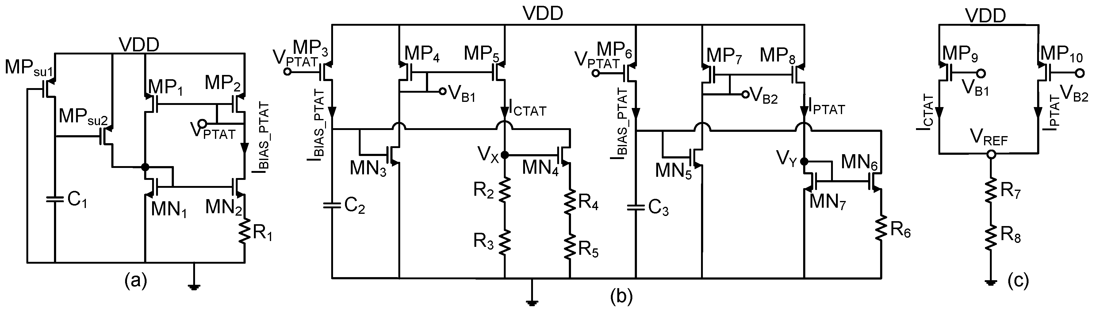
3. Proposed Reference Circuits
In this work, two versions of low-power, subthreshold reference circuits were extensively assessed for the space environment. The design and analog performance tests for non-radiation environments was presented in [
17,
51,
87]. This paper focuses on the radiation tolerance of two subthreshold topologies. The characterization experiments include measured results of the post-fabricated ICs in a wide temperature sweep, as well as measured results after exposing the circuits to
-rays, X-rays, protons and heavy ions (silicon, krypton and xenon).
The designs were fabricated using TowerJazz Semiconductor’s CMOS 0.18 μm technology. Both circuits utilize enclosed layout geometries [
88] for all key NMOS transistors. These use enclosed layout geometry since they are prone to leakage currents from positive charges that are trapped in the deep-trench isolation structure and attract negative charges from the substrate, that form a parasitic channel along the edges of a planar layout geometry. The PMOS transistors are not prone to this effect, since their charge carriers are holes and trapped positive charges in oxide structures decrease the leakage current. The presented circuits are MOS-based voltage references, operating in subthreshold, which combine individually-linearized PTAT and CTAT currents. The proposed topologies incorporate two different types of polysilicon resistors. These, when combined with a subthreshold NMOS transistor, lead to a high-order curvature correction of the reference voltage, giving better performance across a wide range of temperatures. The two topologies have a high-impedance node at the drain of MP
3 transistor of the core structure. In addition, the reference voltage (VR)1 topology has an extra high-impedance node at the drain of MP
6 transistor.
Subthreshold operation of circuits and systems would be extremely beneficial in space microelectronics due to the limited energy sources. However, subthreshold circuits have to prove their reliability for such missions, where several radiation sources impact their electrical parameters. Therefore, this work investigates the resilience of subthreshold circuits with high total doses for a wide range of radiation sources. The circuits under evaluation are designed using the standard radiation-hardening-by-design (RHBD) techniques such as, extensive guard-rings, minimum gate extension to avoid leakage from the channel edge due to shallow trench isolation (STI), small layout and specialized circuit architectures.
The first reference circuit [
51] is a low-power, wide-temperature-range topology which achieves a low TC over a temperature range of 190 °C, whilst being biased at a low supply voltage of 0.75 V and consuming only 4 μW of power. The circuit’s topology is shown in
Figure 1 and its layout in
Figure 2a. This circuit occupies an area of 0.039 mm
2.
The reference output voltage is generated by summing
and
currents across a resistance. This voltage is equal to:
where
. A detailed expression of the first reference voltage (VR1) can be expressed as:
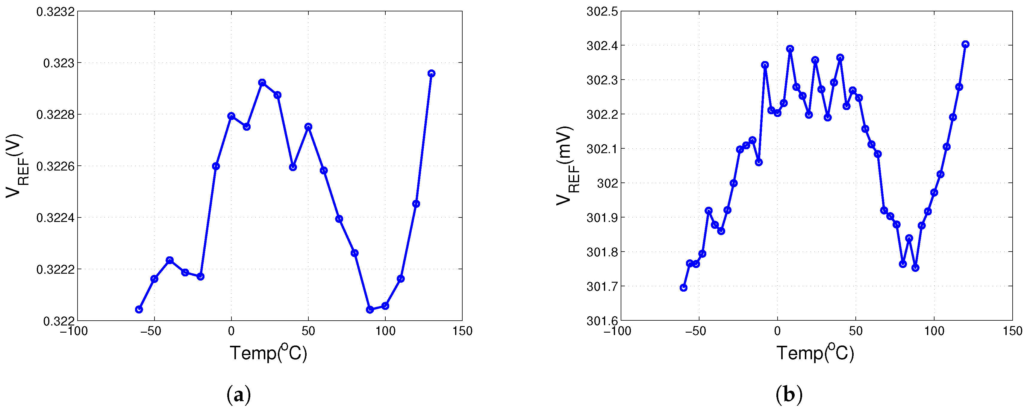
The measured post-trimmed TC at a bias voltage of 0.75 V is 15 ppm/°C for an extended temperature range of 190 °C (−60 °C to 130 °C) and is shown in
Figure 3a.
The second reference circuit [
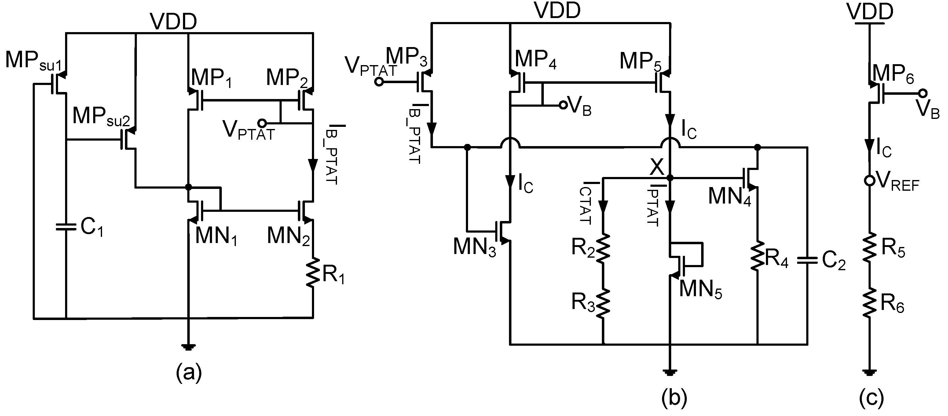
17] is also a low-power, wide-temperature-range, curvature-compensated topology. The proposed topology achieves a temperature sensitivity of 12.9 ppm/°C for a temperature range of 180 °C (−60 °C to 120 °C) at a bias voltage of 0.7 V, whilst consuming 2.7 μW. It occupies an area of 0.023 mm
2.
The schematic of the proposed design is illustrated in
Figure 4 while the layout is shown in
Figure 2b. The topology consists of three main modules. A PTAT circuit, including the start-up circuit (
,
,
), is shown in
Figure 4a, which generates a PTAT current for supplying the module of
Figure 4b [
15,
89].
Figure 4b shows the core module, where both the linear and the non-linear compensation predominantly takes place.
The reference voltage at the output of the proposed topology in
Figure 4 can be expressed as:
where
and the current
consists of the currents through resistors
and
, and the current through the transistor
The detailed equation for the second output reference voltage (VR2) is described by:
where
is:
where
is the mobility of carriers in the device channel,
is the oxide capacitance per unit area and
n is the subthreshold slope factor.
4. Experimental Measurements on SET Irradiation Effects (Heavy Ions)
The proposed reference circuits were characterized at Radiation Effects Facility (RADEF) at the University of Jyvaskyla, Finland, for ASETs. Heavy ions (Si, Kr and Xe) from RADEF’s standard 9.3 MeV/μm cocktail beam were used in order to provide different LET characteristics, so as to extract their cross-section (). The circuit irradiations were performed in air with a Kapton foil thickness of 25 μm and air thickness of 5 mm. During irradiation, the circuits were biased at their nominal supply voltages and the ASETs were recorded using a high sampling-rate oscilloscope (Agilent Technologies, Inc., Santa Clara, California, United States, DSO9104A 1 GHz/20 GS/s). The oscilloscope was set to record all the transient segments above a threshold trigger level (12 mV). This level was higher than the reference circuit noise floor and it ensures that stray electromagnetic fields at the testing facilities would not trigger the oscilloscope.
The RADEF’s heavy ions cocktail provided Si ions with a LET(Si) of ∼6.9 MeV·cm2/mg, Kr ions with a LET(Si) of ∼36.1 MeV·cm2/mg and Xe ions with a LET(Si) of ∼64.7 MeV·cm2/mg. The charge deposited in the targeted material is greater at higher value of LET.
The cross-section,
, is a metric to evaluate the resilience of the circuits under test when exposed to heavy-ions and can be expressed as:
where
is the observed number of ASET events and
is the uniform particle fluence (particles/cm
2).
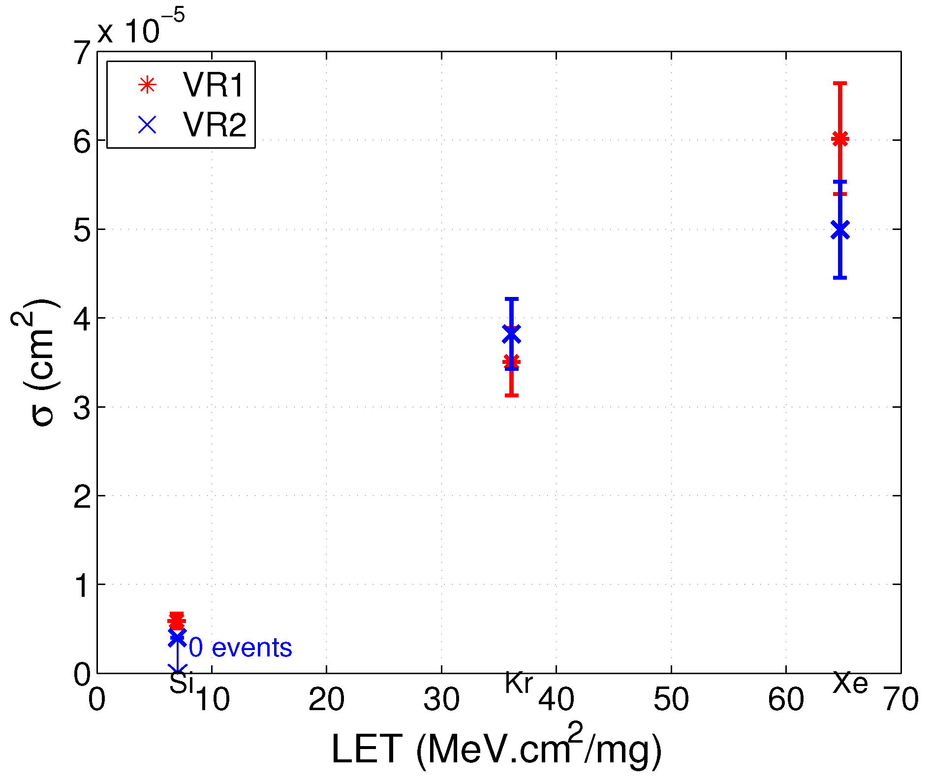
The measured
of the two voltage references are shown in
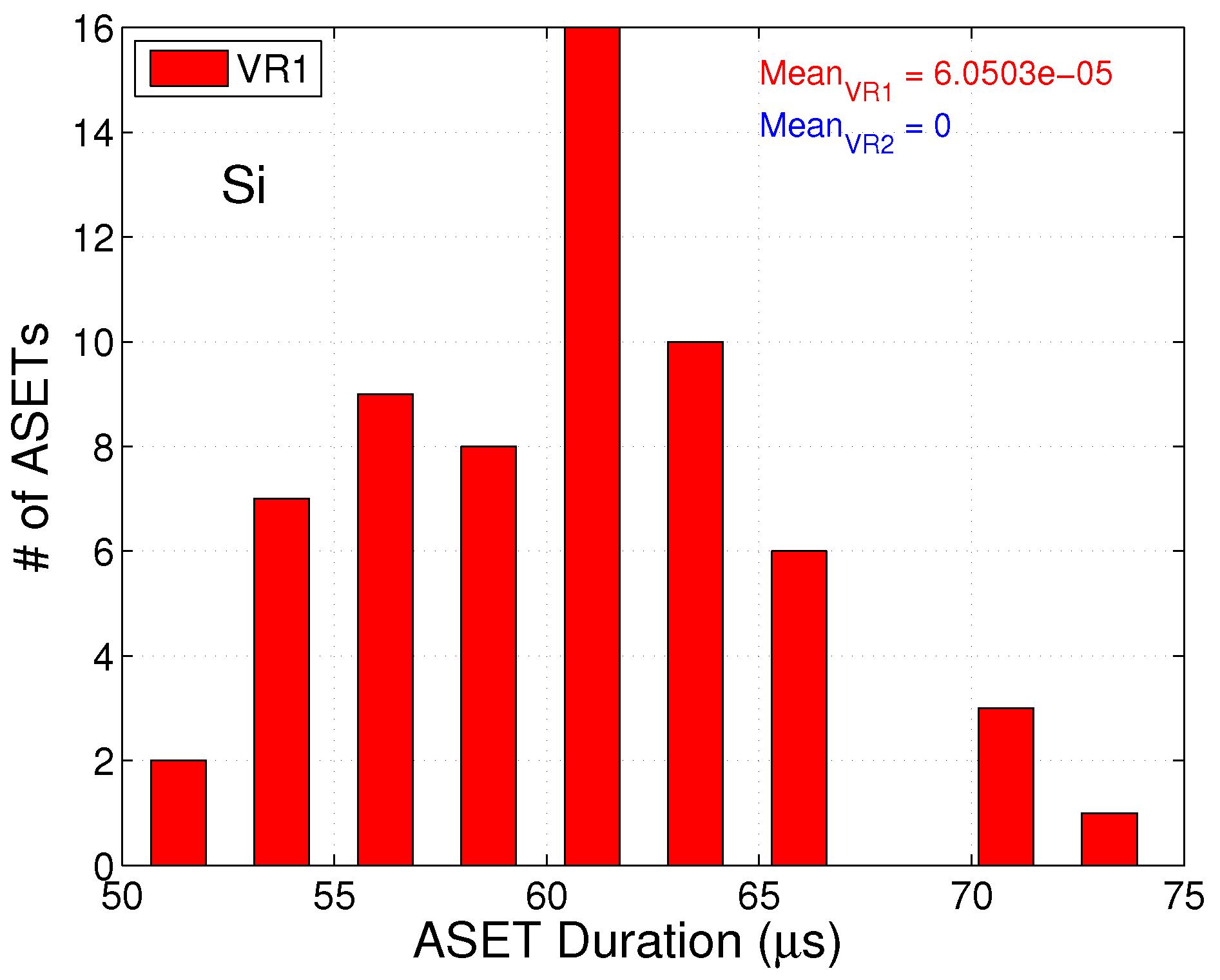
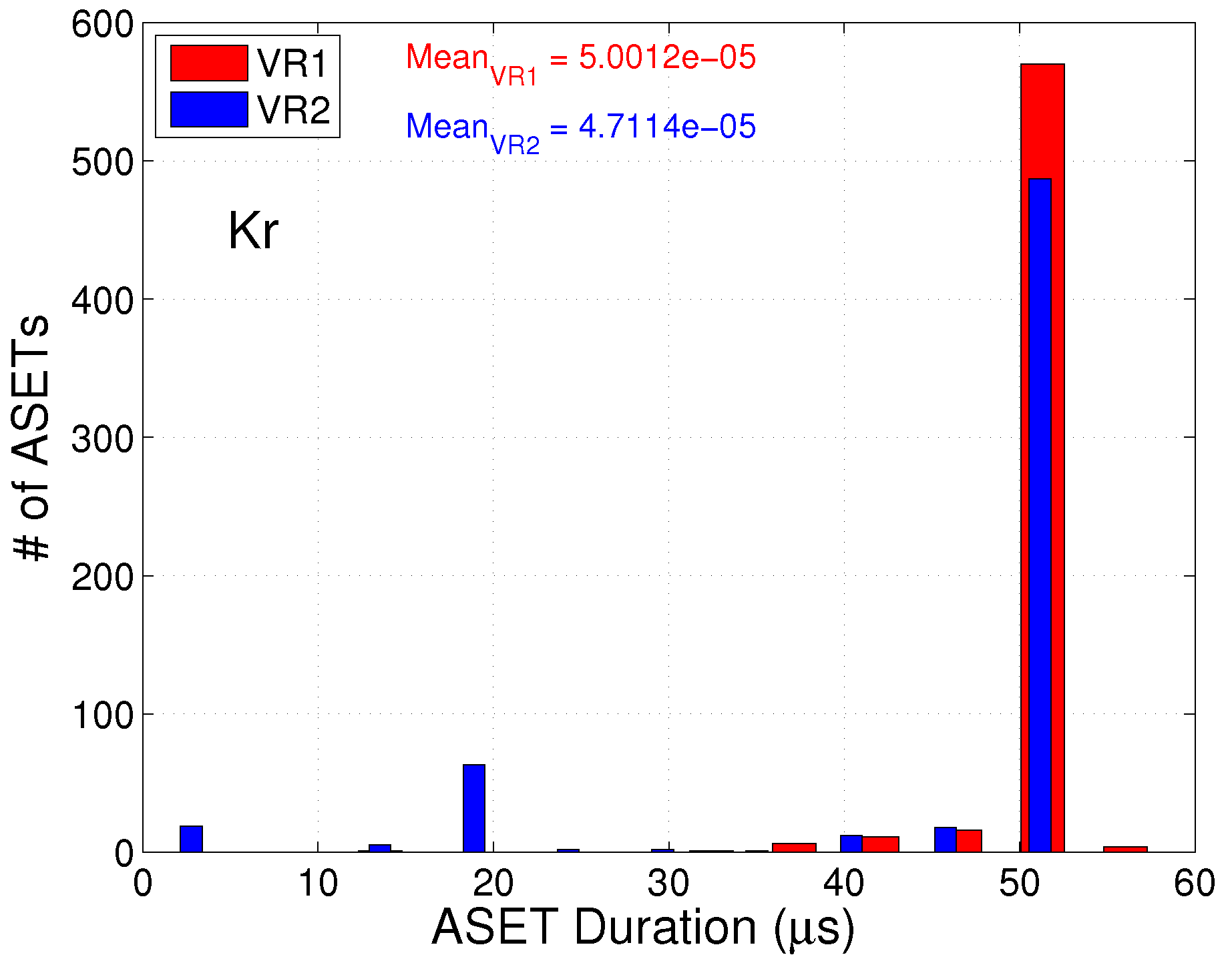
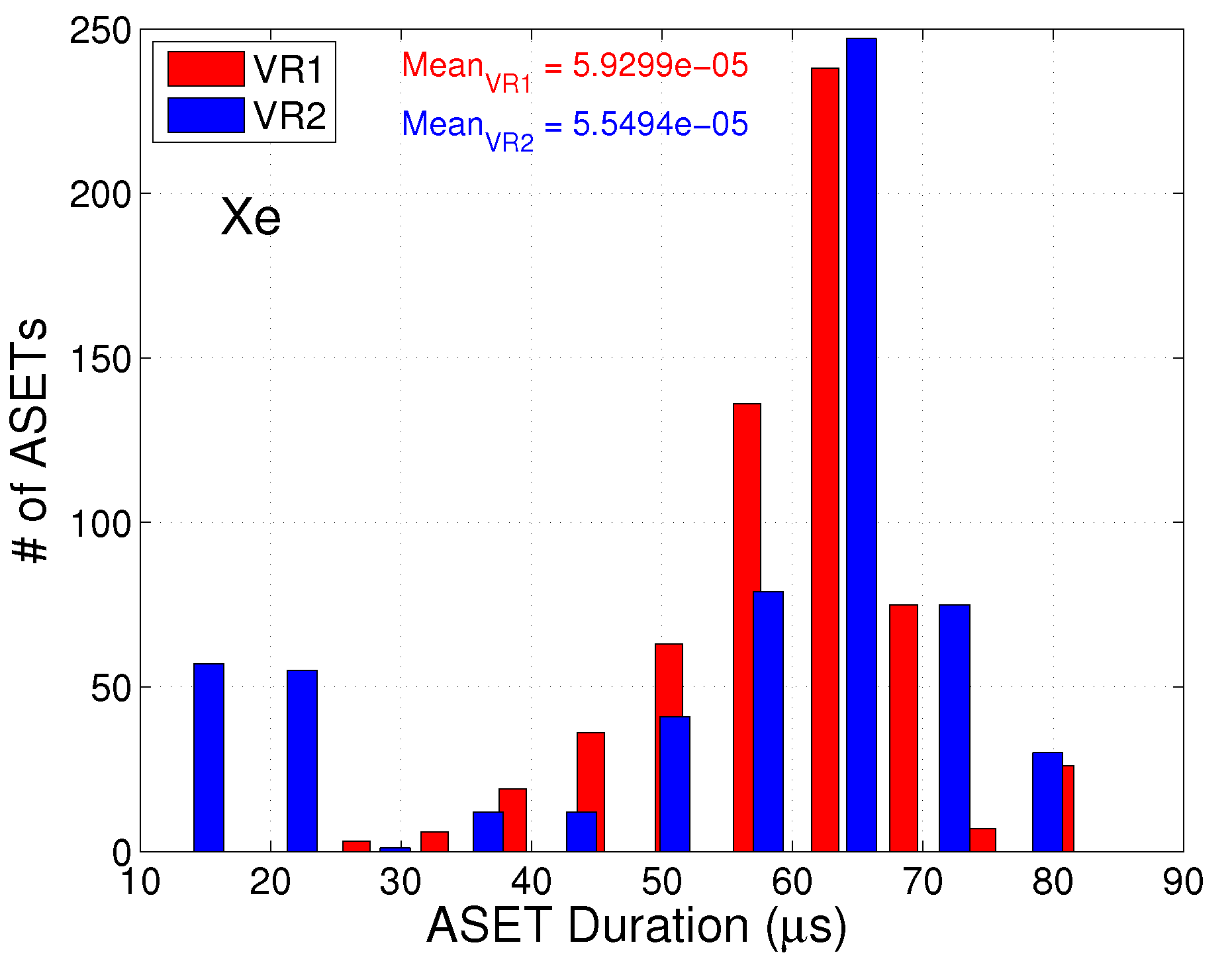
Figure 5. The VR2 topology did not exhibit any sensitivity to Si ions, while an overall comparison shows that VR2 had less sensitivity compared to the VR1 circuit. The measured SET durations for the two circuits (VR1 and VR2) are shown in
Figure 6,
Figure 7 and
Figure 8 for silicon, krypton and xenon respectively. The VR2 circuit exhibits lower transients’ duration compared to VR1.
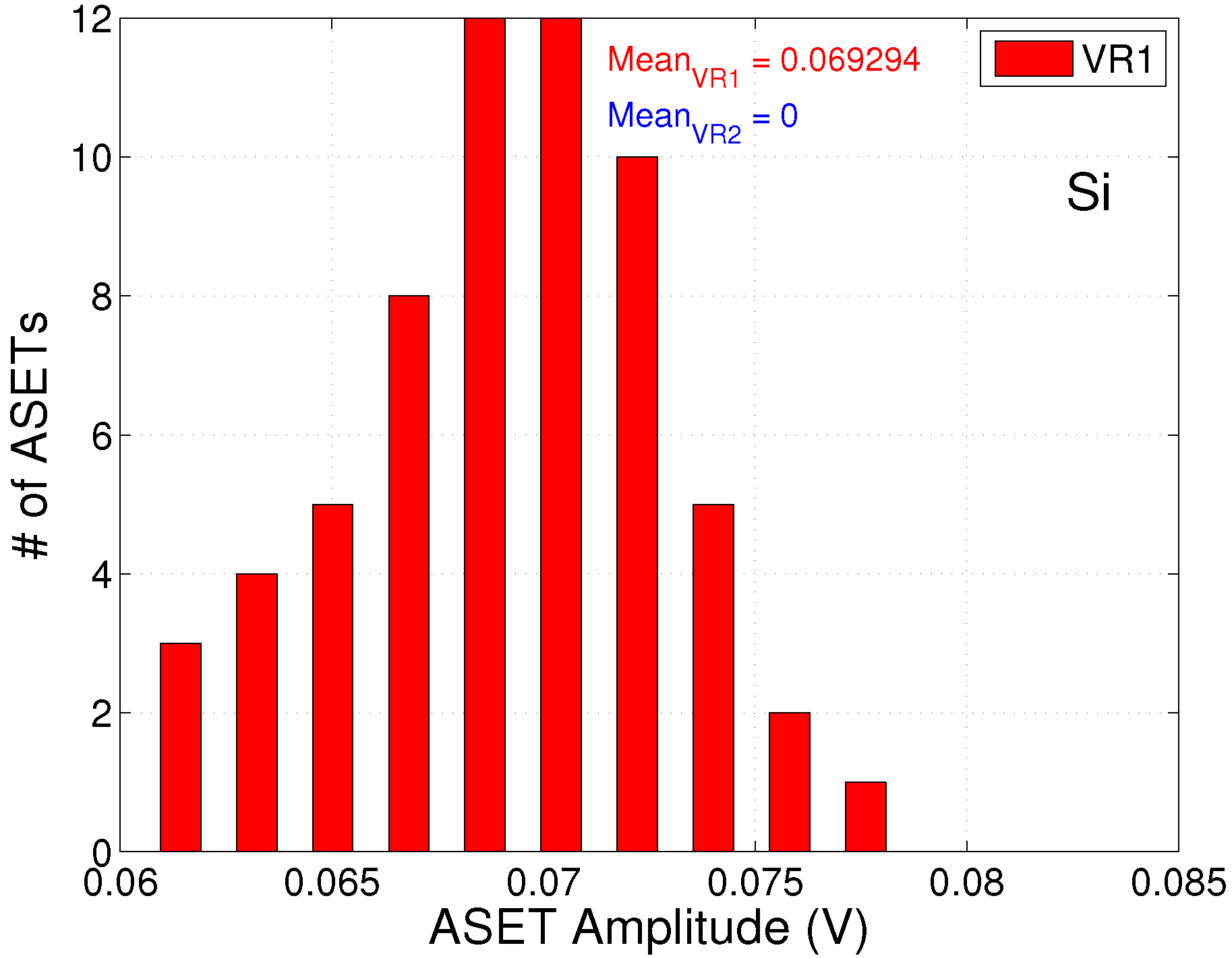
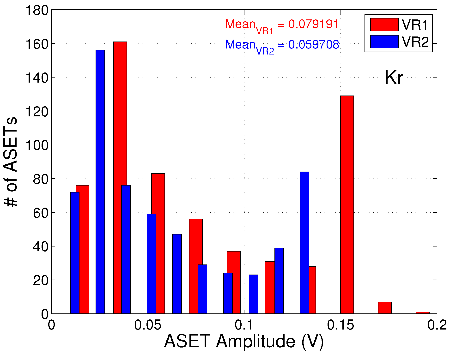
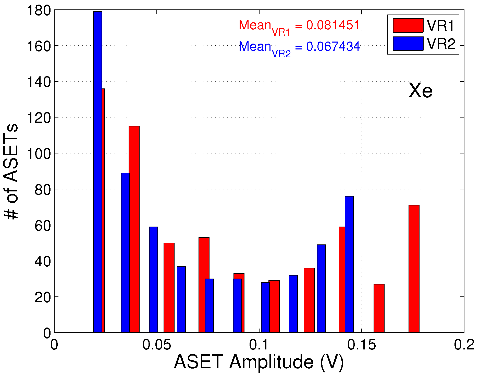
The measured SET amplitudes for the two circuits (VR1 and VR2) are shown in
Figure 9,
Figure 10 and
Figure 11 for silicon, krypton and xenon respectively. The VR2 circuit exhibits smaller amplitudes compared to VR1.
The fact that VR2 outperforms VR1, in terms of , SETs’ durations and amplitude, is possibly due to the smaller area of VR2 compared to VR1, since their circuit topology and operating conditions are very similar.
In general, the subthreshold circuits show somewhat higher sensitivity to heavy ions, in terms of
and SETs’ durations, compared to the strong inversion ones which were evaluated in previous work [
90] by the authors. This is partly due to the lower supply voltage, which in turn needs less amount of deposited charge from the impinging ion in order to alter their nominal operating conditions of a particular circuit node. Furthermore, subthreshold circuits need more time to recover from a transient because of the lower current drive capability and the slower feedback. However, due to the limited bandwidth, longer transient durations are required in order to appear at the output, which gives subthreshold circuits an advantage. Part of the higher sensitivity could also be attributed to the larger silicon area of those topologies compared to the ones in [
90]. The SETs’ amplitudes in subthreshold and strong inversion circuits in [
90] are comparable. This is probably due to the same reason described above, where the larger time constants of the subthreshold circuits tend to filter out some of the transients. An additional advantage of subthreshold circuits when exposed to heavy ions is that it is less probable to latch-up due to parasitic bipolar effect because of much smaller currents. This is a big advantage since parasitic bipolar effect could be fatal for a device and therefore an entire system.
5. Experimental Measurements on TID Irradiation Effects (-rays and X-rays)
In this section, a complete experimental characterization under -rays and X-rays TID induced effects was performed in order to evaluate the resilience of subthreshold reference circuit topologies against TID.
5.1. -ray Irradiation
The -ray irradiation was performed at the Radiation Physics Laboratory of the Universidade de Santiago de Compostela, using an AECL Theratron 780 Co-60 unit at room temperature. Dose rate and TID were monitored in real time by a 0.6 cm3 therapy level ionization chamber connected to a reference class electrometer. The chamber and chips were positioned behind a 2 mm lead slab and 1 mm aluminium slab, to provide transient charge particle equilibrium in the gamma-ray field originating from the Co-60 source. Measured charge was converted to absorbed dose in air first, by employing the value of mean energy to produce a pair in air by a Co-60 beam ( = 33.97 J/C) and the mass of air enclosed in the chamber cavity with the appropriate correction due to ambient conditions. The correction factor between dose in air and dose in silicon inside the chips was calculated by Monte Carlo simulations (EGSnrc code) employing a realistic definition of geometries of the therapy unit, the ionization chamber and the chips.
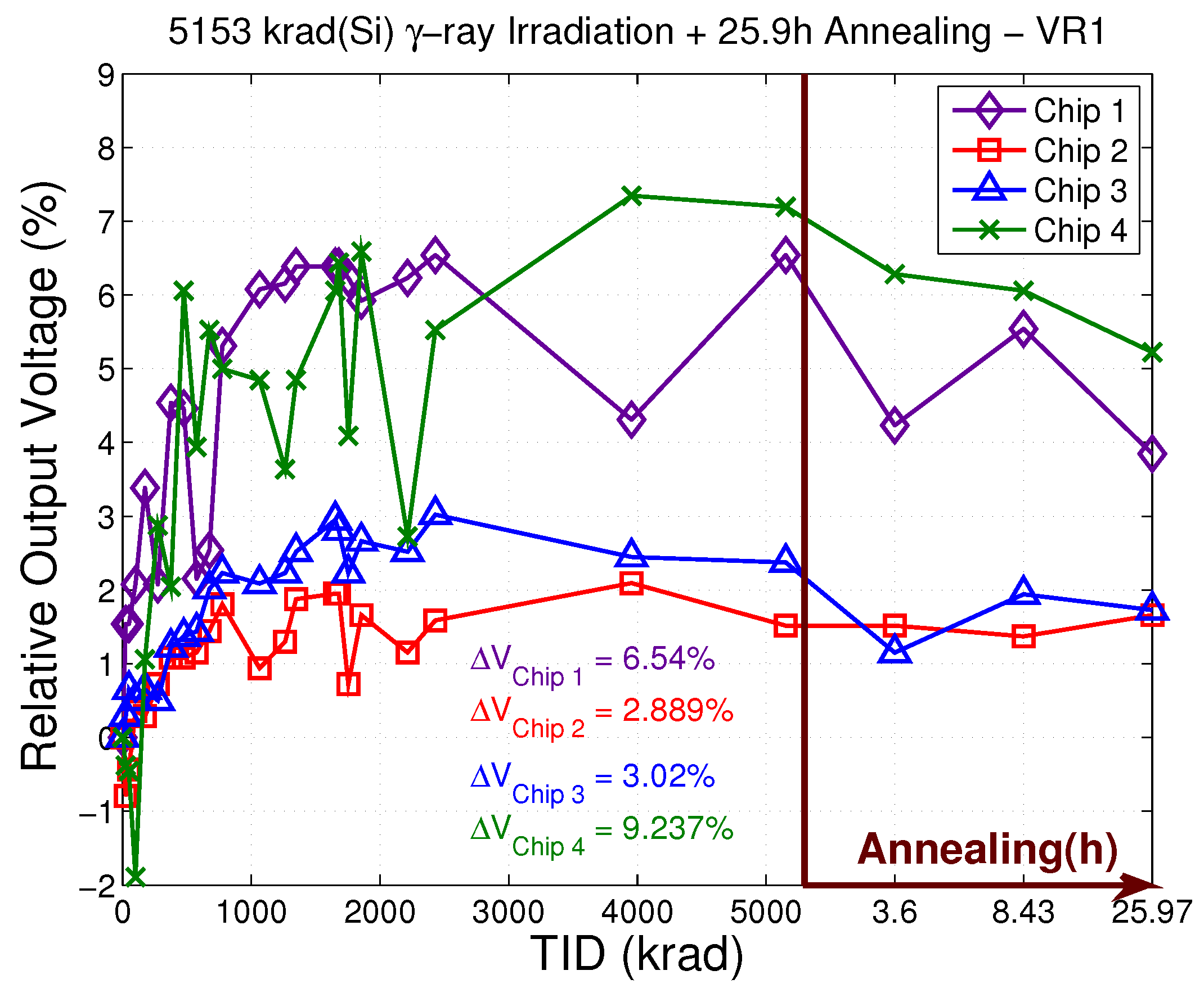
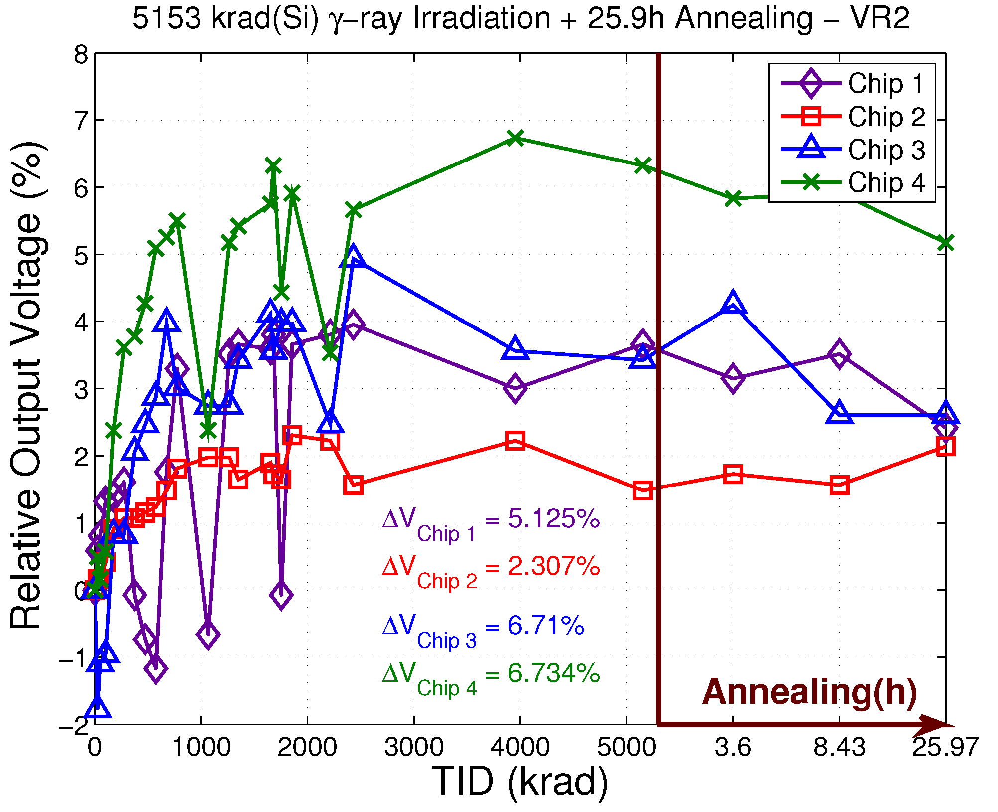
Four chips from two different wafers (two chips from each wafer) were irradiated with
-rays at a dose rate of 25 krad/h(Si) up to a total dose of 5.153 Mrad(Si), followed by room temperature annealing steps with the last annealing step measurement taken 25.97 h after the end of irradiation. The circuits under test were irradiated and measured at room temperature, with the supplies biased at nominal voltage during irradiation. The output voltages and current consumption of each circuit were measured at regular dose steps. The measured results of the relative output voltage are shown in
Figure 12 for VR1 circuit and
Figure 13 for VR2 circuit. Different wafers are expected to have some variation on device parameters, like threshold, voltage due to process variations. The measured results of the relative current consumption are shown in
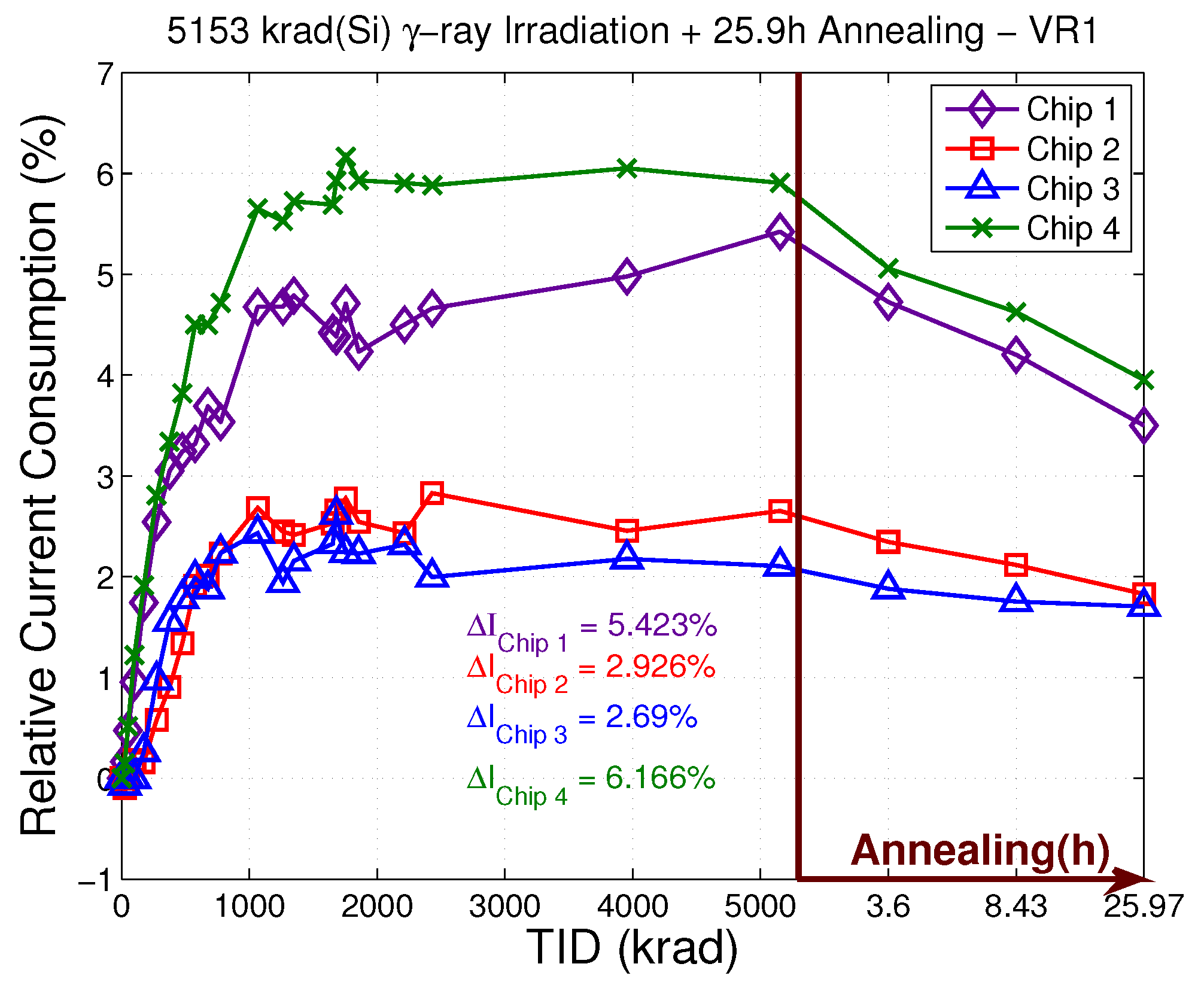
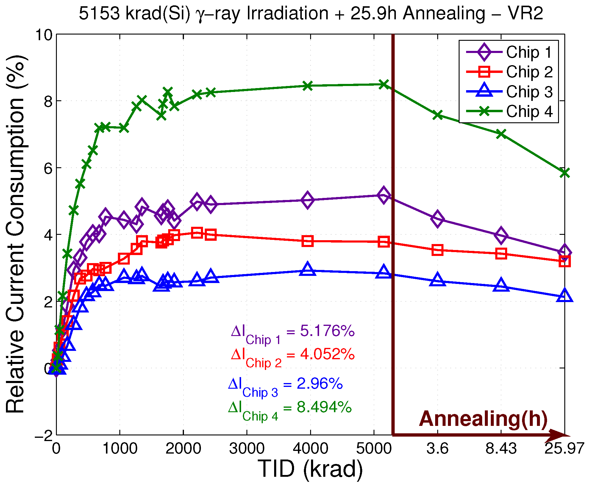
Figure 14 for VR1 circuit and
Figure 15 for VR2 circuit.
The smallest output voltage variation is achieved by the VR2 circuit of chip 2 which is
and the highest by the VR1 circuit of chip 1 which is
. The two voltage references (VR1 and VR2) show comparable performance in terms of
-rays irradiation TID effects, which for some of the chips is remarkable when considering the high total dose. The variation between different chips is due to the device mismatch within a circuit as well as due to process variation between different dies. Both circuits show a rising trend for total doses up to 1 Mrad, while for higher doses the output voltage remains almost unaffected. This could be explained by the competition between the interface state trapped charge and the oxide trapped charge. The interface state trapped charge occurs much slower and has a counterring effect in NMOS devices as opposed to the oxide trapped charge. Furthermore, when activated, interface trapped charge dominates the oxide trapped charge. The measured relative current consumption in
Figure 14 and
Figure 15 show a similar trend with the relative output voltage variations. The current consumption variations are due to threshold voltage induced drain current variations as well as edge leakage currents due to STI trapped charge. During annealing at room temperature, the output voltage and current consumption partially recover. However, the interface trapped charge would need very high temperatures in order to anneal.
5.2. X-rays Irradiation
Two sessions of X-rays irradiation were performed. The first session was performed up to a total dose of 3.7 Mrad(Si) at the Radiation Physics Laboratory of the Universidade de Santiago de Compostela. The second session was performed up to a total dose of 80 Mrad(Si) at the Department of Information Engineering of the University of Padova. During both irradiation sessions all the circuits within the chips were biased at nominal supply voltage and their output reference voltages were measured at regular dose steps during irradiation.
5.2.1. X-ray Irradiation up to 3.17 Mrad(Si)
The irradiation was performed by a TW50 X-ray beam, delivered by an Oxford Instruments Neptune tube, with an added filtration by 1.1 mm of aluminum. X-ray beam outputs are generally measured by means of thin entrance window air filled ionization chambers. Conversion to absorbed dose to a relatively high atomic matter (high Z) medium like Silicon, surrounded by other higher than air Z materials, such as those present in a silicon chip, is not trivial. This is because the ratio of the absorbed dose to silicon and absorbed dose to air in the chamber varies sharply as a function of X-ray photon energy, due to enhanced photoelectric effect cross section. The beam output was characterized by measuring the X-ray spectrum and the exposure rate. The spectrum was measured with an AMPTEK CdTe scintillator connected to a MultiChannel Analyzer (MCA). The 50 keV tail was employed to calibrate the MCA in terms of photon energy. The exposure rate was measured with a PTW 23344 plate parallel X-ray chamber connected to an IBA DOSE-1 electrometer. The measured exposure rate was first converted to absorbed dose in air and then to absorbed dose in silicon in the area of the circuits under test. This was done by employing EGSnrc Monte Carlo code. The measured spectrum was used as the energy distribution of the Monte Carlo primary source. This spectrum was fine-tuned in order to reproduce experimental percent depth doses of the unfiltered 50 keV beam. A conversion factor was determined as the ratio of Monte Carlo absorbed dose in silicon inside the circuits under test and Monte Carlo absorbed dose to air inside the ionization chamber cavity.
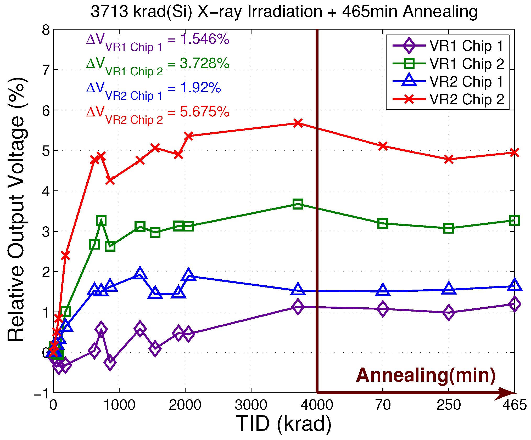
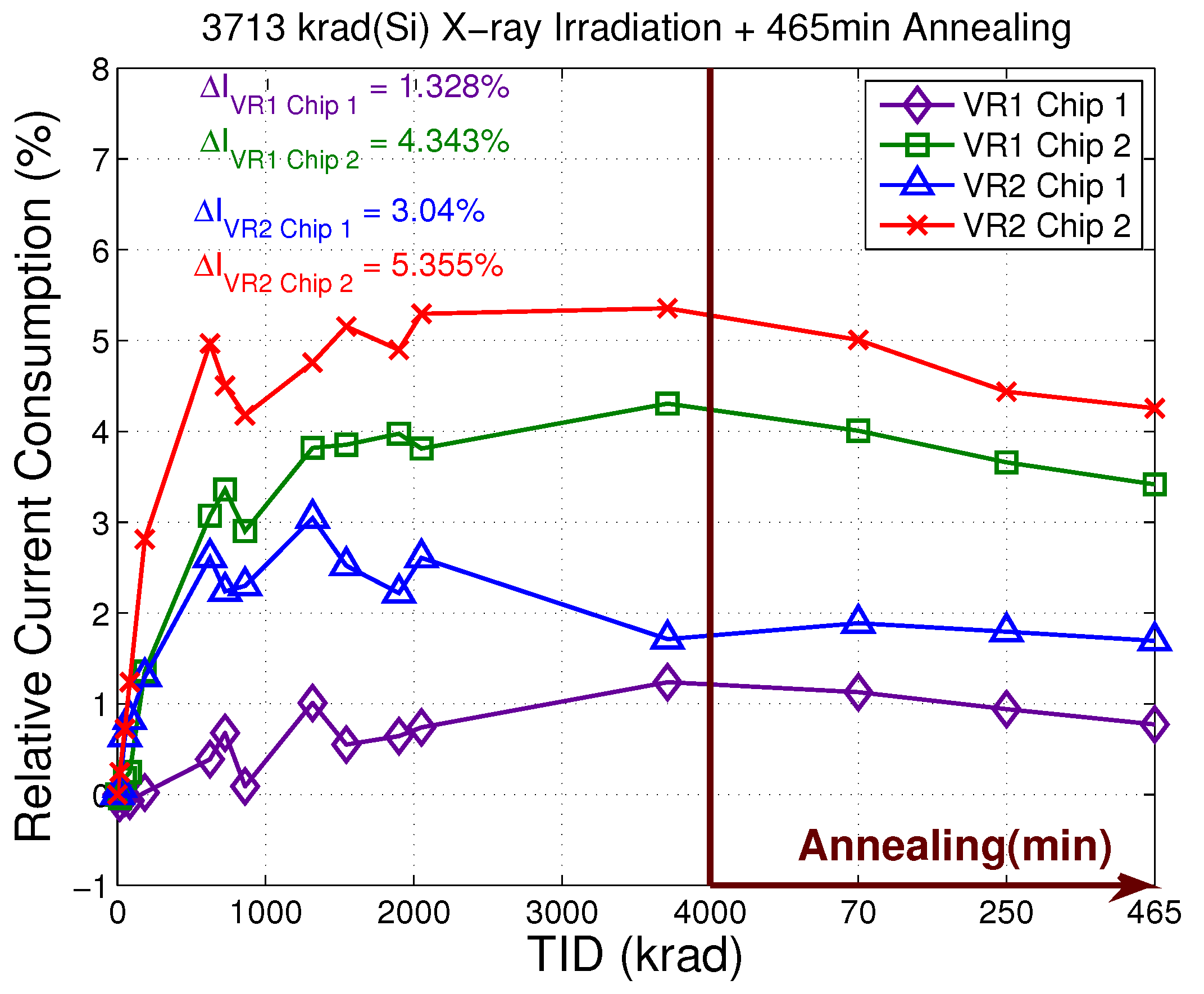
In this first session, the two chips were irradiated with X-rays using a dose rate of 8.75 rad(Si)/s up to a total dose of 1.3 Mrad(Si) and then irradiated with a dose rate of 6.56 rad(Si)/s, up to a total dose of 3.173 Mrad(Si). The circuits were irradiated and measured at room temperature, with their supplies biased at nominal supply voltage. The output voltages as well as the current consumption were measured at regular dose steps during irradiation. Annealing steps at room temperature followed the irradiation, with the last annealing measurement taken 465 min after the end of irradiation. The measured results of the relative output voltage of the two chips of VR1 and VR2 reference circuits are shown in
Figure 16 and their relative current consumption is shown in
Figure 17.
The smallest output voltage variation was achieved by the VR1 circuit of chip 1 which was and the highest by the VR2 circuit of chip 2 which was . The variation between different chips is again due to the process and mismatch variations between the circuits’ devices. This can be justified by the fact that all the circuits of chip 1 demonstrated better performance than the ones of chip 2. Both circuits showed changing properties trend for total doses up to 800 krad, which then stabilizes at higher doses. This effect was in agreement with the -rays experiments and can be explained by the opposite effect of the interface state trapped charge and the oxide trapped charge on the device characteristics.
The measured relative current consumption in
Figure 17 show almost identical trend with the relative output voltage variations. The current consumption variations can be attributed to the threshold voltage variation induced drain current variation as well as edge leakage currents due to STI trapped charge. During annealing at room temperature, the output voltage and current consumption of the VR1 and VR2 circuits of chip 2 (exhibited the highest TID variation) showed some recovering, while the corresponding circuits of chip 1 did not exhibit any significant change.
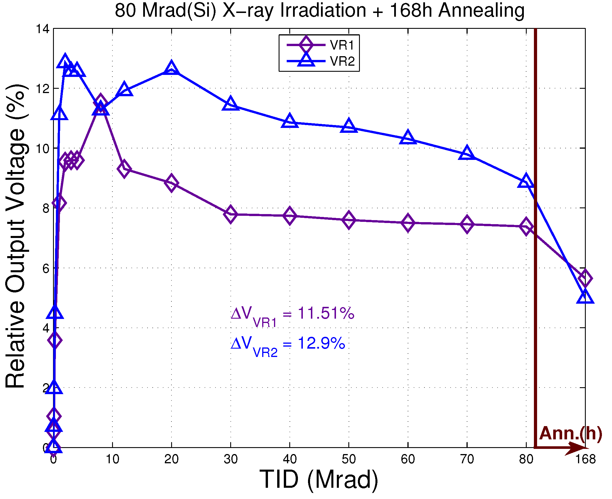
5.2.2. X-ray Irradiation up to 80 Mrad(Si)
In this session, a chip with the circuits under test was irradiated at a room temperature at the Department of Information Engineering of the University of Padova with 10-keV X-rays using a dose rate of 300 rad(Si)/s up to a total dose of 80 Mrad(Si). During irradiation both the circuits were biased at their nominal supply voltage. The output voltages were measured at regular dose steps during irradiation as well as during room temperature annealing, after the end of irradiation. The measured results for the relative output voltage are shown in
Figure 18.
The two circuits showed similar performance to TID induced effects, where the smallest output voltage variation was achieved by the VR1 circuit which was
and the highest by the VR2 circuit which was
. The TID induced output voltage variations as shown in
Figure 18 revealed an important outcome. Both circuits exhibited significant changes up to 10 Mrad, while for higher total doses they stabilized and then recovered significantly. This is in agreement with
-rays and X-ray experiments and could again be explained by the competition between the interface state trapped charge and the oxide trapped charge. Another reason for this recovering during irradiation is the possible saturation of the oxide trapped charge first and then the interface trapped charge, which can be caused by the high total dose exposure. This can be supported by (
1) and (
2), where the irradiation induced rate of threshold voltage shift will reduce from square to linear dependence on oxide thickness. During annealing, at room temperature, the output voltage recovered at a higher rate.
6. Experimental Measurements for TID and DD Irradiation Effects (Protons + X-rays and Protons)
The space radiation mixture is to a large extent composed from high-energy protons [
91]. Therefore, in this section, the different topologies were irradiated with protons and X-rays and only-protons for the experimental characterization of DD/TID radiation-induced effects. These tests were required in order to classify the robustness of the subthreshold circuits in a more realistic scenario. It has to be noted that the effects induced by DD and TID interacted in a complicated fashion and were not simply additive [
91].
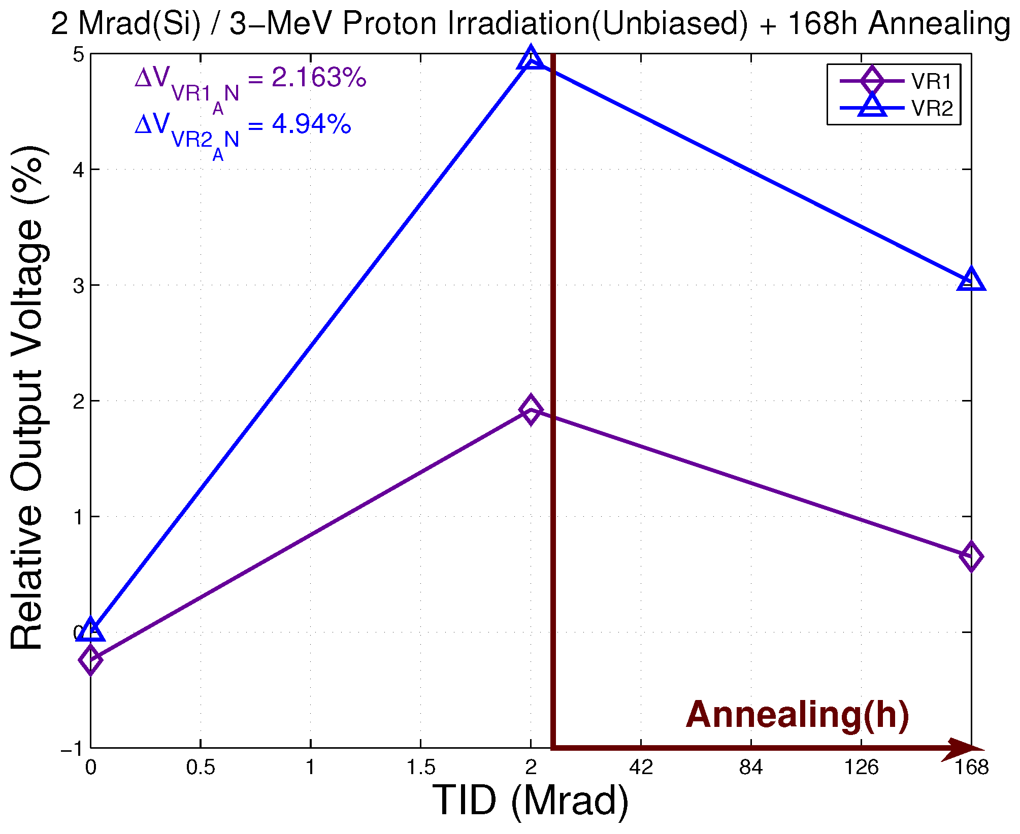
6.1. Irradiation with Protons and X-rays
In this session the chip with the two circuits was irradiated with a 3 MeV proton beam in vacuum, with a flux of 10
9 p/cm
2·s, up to a fluence of 1.47 × 10
12 p/cm
2, corresponding to a total ionizing dose of 2 Mrad(Si). This was followed by three days of room temperature annealing. The circuits were unbiased during irradiation and they were biased just after the end of the irradiation in order to measure their output voltage. Then, they were remeasured again after one week (168 h) of room temperature annealing. The results of this irradiation session are shown in
Figure 19 for the relative output voltage versus TID.
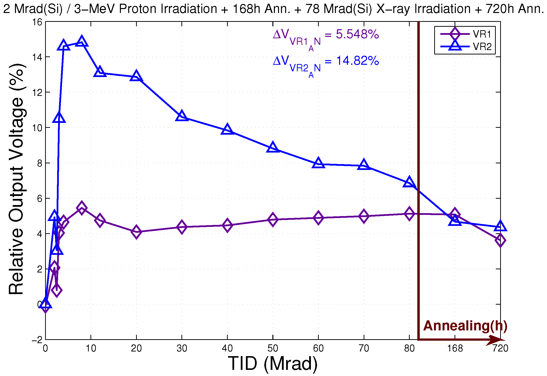
The same chip, that was irradiated with a total dose of 2 Mrad(Si) of protons, was further irradiated with 10 keV X-rays after the proton exposure and annealing step. The X-ray irradiation and subsequent annealing were performed at room temperature, with all the circuits biased at the nominal supply voltage. A total dose of 78 Mrad(Si) was delivered through this X-ray irradiation session, so that a total dose of 80 Mrad(Si) was accumulated on the device, using a dose rate of 300 rad(Si)/s. The output voltages were measured at regular dose steps during irradiation at room temperature. Annealing steps followed the irradiation at room temperature, with the last annealing measurement taken one month (720 h) after the end of irradiation.
The results of the proton and subsequent X-ray irradiation are shown in
Figure 20. The total dose reported on the X-axis of
Figure 20 is the sum of the proton and the subsequent X-rays irradiation.
The VR1 circuit topology shows more resilience in comparison to the VR2 topology. The differences of the output voltage in
Figure 20 when compared to the same irradiation dose of
Figure 18 is possibly due to displacement damage that was induced from the proton irradiation on the subthreshold biased transistors. A 3 MeV proton beam with such a high fluence (1.47 × 10
12 p/cm
2) delivered both, TID as well as DD, for the equivalent dose of about two Mrad(Si). The conduction of a MOS transistor in sub-threshold regime was due to diffusion of minority carriers in the channel, where minority carrier lifetime was affected by DD in a similar manner as in bipolar transistors.
6.2. Irradiation with Protons
In this irradiation session, another chip was irradiated in air with protons, at the Svedberg Laboratory in the University of Uppsala. The nominal primary proton energy was 180-MeV. In order to create a uniform proton field at the position of the chips under test, the primary proton beam was scattered by a Ta foil of 1.5 mm thickness. The chips were positioned at a distance of 200 cm from the foil. The average proton energy at the chips under test position amounted to 170.5-MeV. During irradiation, the incident proton beam was monitored by a telescope consisting of two scintillators, calibrated using a thin-film breakdown counter equipped with a fission foil. The telescope detected protons scattered by a stainless steel foil at the end of the vacuum pipe.
The chip was irradiated with the 170.5 MeV protons at the fluence of cm−2. By the end of the experiment it had accumulated a total dose of 1400 krad(Si), at steps of 25 krad for low TID values, with wider steps for higher TID values, with an intermediate annealing step of 15 h. The irradiation and measurements were performed at room temperature with all the circuits biased at nominal supply voltage.
The output voltage of the circuits was measured at regular dose steps and is shown in
Figure 21, where VR1 outperforms VR2. Both circuits show a considerable change for total doses up to 900 krad, which saturates at higher doses. This again agrees with the experimental sessions of
-rays and X-rays and could be attributed to the same reasons explained above. The relative current consumption is shown in
Figure 22 where the current consumption trend was identical with the relative output voltage variations trend. This is because the STI edge leakage current as well as the threshold voltage shift variations (gate oxide and interface states trapped charge) modify the current drained by the transistors and therefore the total current consumption of the circuits was modified accordingly. The current was increased mostly in the non-core NMOS transistors where planar layout was utilized. However, all transistors (including enclosed layout geometry ones) had small current variations due to threshold voltage shifts. During annealing both circuits show significant recovery in terms of output voltage as well as current consumption due to possible annealing of oxide trapped charge.
7. Discussion on Subthreshold Radiation Effects
In this paper we have presented the results of radiation tests involving two subthreshold circuits. When comparing TID radiation-induced effects between subthreshold and strong inversion circuits, the major difference is the dependence of the drain current to threshold voltage shift. This dependence is exponential in subthreshold circuits as opposed to square-law dependence in strong inversion circuits. This is the major disadvantage of subthreshold circuits in radiation environment, however this disadvantage is rapidly diminishing in deep sub-micron semiconductor technologies, where according to (
1) and (
2) the oxide thickness reduction will diminish the radiation-induced threshold voltage shift. Thus, in deep sub-micron technologies, subthreshold circuits will potentially emerge as an attractive and promising solution for space microelectronics. The leakage currents due to trapped charge at the STI oxides will have more relative impact in subthreshold circuits compared to strong inversion ones, since the actual current through the channel could be in the order of the STI induced leakage currents. However, this disadvantage, which concerns only NMOS devices, can be remedied by using enclosed layout geometry transistors at the layout level. On the other hand, the low-voltage operation of subthreshold circuits applies lower electric fields across the oxides. This will reduce the rate of electron–hole separation and increase the probability of recombination. Therefore, this induces lower trapped charge in the oxides and hence lower will be the radiation-induced threshold voltage shift and leakage current.
SETs usually originate from particle strikes which traverse reverse-biased pn-junctions or areas with strong electric fields. Built-in electric fields or fields created by normal biasing conditions separate the pairs, leaving excess charge after the event. This is particularly a problem at the transistor’s drain terminal, especially with the deep submicron technologies, where the generated plasma of e-h pairs drifts apart because of the high electric fields across the depletion region. When comparing SET radiation-induced effects between subthreshold and strong inversion circuits, the major difference is the supply voltage. The gate oxide thickness (depends on the type of device that is selected) and the supply voltage, both affect the amount of energy needed in order to alter the transistor’s normal operating conditions. Therefore, the lower supply voltage of subthreshold circuits will require less charge and therefore less energy from the impinging ion in order to alter its nominal state, which makes them more vulnerable compared to strong inversion circuits. On the other hand, the advantage of low-voltage operation of subthreshold circuits is the lower electric field across the pn-junctions which reduces the amount of separated e-h pairs as well as the charge collected at the impinged node. An additional advantage of subthreshold circuits is that it is not possible to form a BJT through the substrate (parasitic bipolar effect) after a heavy ion strike [
46].
An important advantage of subthreshold regime, which applies in both TID and SET effects, is that the drain-source voltage for saturation is 4 kT ≈ 104 mV which, in contrast with strong inversion regime, is very low and independent of the gate-source voltage and threshold voltage. Therefore, in contrast with strong inversion regime, it is not easy to get a subthreshold transistor out of saturation region due to irradiation-induced effects. This has been proven throughout all the experimental sessions in this work, where there was not any complete functional failure observed, even in very high TID irradiation or heavy ion strikes.
8. Conclusions
A comprehensive evaluation of two subthreshold voltage reference circuits with respect to their resilience to SEE, TID and TID/DD was performed. The evaluation is supported by measured results with -rays, X-rays, protons and heavy ions. The high total doses applied in this range of experiments provide a complete evaluation of subthreshold circuits in the whole range of space applications, radiation physics instruments and medical applications.
The fact that VR2 outperforms VR1, in terms of , and SETs’ durations and amplitude, is due to the smaller area of VR2 compared to VR1. The circuit topology and operating conditions of the two circuits are very similar, since VR2 combines two feedback loops within a single branch.
The critical nodes that affect the output voltage are those that generate and , namely nodes and in VR1 and node X in VR2. The reason that the VR1 circuit outperforms the VR2 circuit in the TID experiments is because VR1’s critical nodes have a slightly higher impedance than that of VR2, given that in VR2 the and appear in parallel at a single node X. Therefore if the TID reduced the threshold of the change in voltage at node X will create a greater change in current at node X, given the lower impedance, when compared to the equivalent critical nodes in VR1. In VR1 the threshold change will influence and , which influence the voltage at the higher impedance nodes and , thus leading to smaller relative change in the output current and consequently reference voltage.
In general, the subthreshold reference circuits show promising performance for space applications, especially in high total doses where they stop deviating or partially recover towards their nominal performance. It is also important that they do not show any signs of collapse or functional failure in any of the experiments, even in uncommonly high total ionization doses or heavy ion strikes. In addition, as expalined above, they will benefit from more advanced technology nodes with thinner gate oxides. These conclusions, along with their main advantage of low-power consumption, make subthreshold circuits candidates for future space missions due to significantly reducing the size, cost and power requirements of space applications. Therefore, there is still room to explore more in the future in terms of different types of circuits and devices.
Author Contributions
Conceptualization, analysis, original draft and revised manuscript preparation: C.M.A. and J.G.; design and execution of the irradiation experiments: C.M.A., D.M.G.-C., S.G., M.B., F.G.R., A.P., A.V.P., A.J., A.V., V.L., C.C., D.N. and J.G.
Funding
This work was supported by: European Union SkyFlash Project 262890 FP7-SPACE-2010-1 (SPA.2010.2.2-01 Space technologies), European Space Agency (ESA/ESTEC Contract 4000111630/14/NL/PA) and, Academy of Finland under the Finnish Centre of Excellence Programme 2012–2017 (Project No 2513553, Nuclear- and Accelerator- Based Physics).
Conflicts of Interest
The authors declare no conflict of interest. The funders had no role in the design of the study; in the collection, analyses, or interpretation of data; in the writing of the manuscript, or in the decision to publish the results.
References
- Arbat, A.; Calligaro, C.; Dayan, V.; Pikhay, E.; Roizin, Y. SkyFlash EC project: Architecture for a 1Mbit S-Flash for space applications. In Proceedings of the 2012 19th IEEE International Conference on Electronics, Circuits and Systems (ICECS), Seville, Spain, 9–12 December 2012; pp. 617–620. [Google Scholar]
- Tsividis, Y.P. Accurate analysis of temperature effects in Ic − Vbe characteristics with application to bandgap reference sources. IEEE J. Solid-State Circuits 1980, 15, 1076–1084. [Google Scholar] [CrossRef]
- Malcovati, P.; Maloberti, F.; Fiocchi, C.; Pruzzi, M. Curvature-compensated BiCMOS bandgap with 1-V supply voltage. IEEE J. Solid-State Circuits 2001, 36, 1076–1081. [Google Scholar] [CrossRef] [Green Version]
- Rincon-Mora, G.A.; Allen, P.E. A 1.1-V current-mode and piecewise-linear curvature-corrected bandgap reference. IEEE J. Solid-State Circuits 1998, 33, 1551–1554. [Google Scholar] [CrossRef]
- Moreira, P. Radiation Effects on the “CERN_bandgap” Circuit. Available online: http://proj-qpll.web.cern.ch/proj-qpll/images/bandgapRadEffects.pdf (accessed on 16 May 2019).
- Georgiou, J.; Toumazou, C. A 126 μW cochlear chip for a totally implantable system. IEEE J. Solid-State Circuits 2005, 40, 430–443. [Google Scholar] [CrossRef]
- Banba, H.; Shiga, H.; Umezawa, A.; Miyaba, T.; Tanzawa, T.; Atsumi, S.; Sakui, K. A CMOS bandgap reference circuit with sub-1-V operation. IEEE J. Solid-State Circuits 1999, 34, 670–674. [Google Scholar] [CrossRef]
- Basyurt, P.B.; Bonizzoni, E.; Aksin, D.Y.; Maloberti, F. A 0.4-V Supply Curvature-Corrected Reference Generator with 84.5-ppm/°C Average Temperature Coefficient within −40 °C to 130 °C. IEEE Trans. Circuits Syst. II Express Briefs 2017, 64, 362–366. [Google Scholar] [CrossRef]
- Huang, Y.; Zhu, L.; Kong, F.; Cheung, C.; Najafizadeh, L. BiCMOS-Based Compensation: Toward Fully Curvature-Corrected Bandgap Reference Circuits. IEEE Trans. Circuits Syst. I Reg. Pap. 2017, 64, 1210–1223. [Google Scholar] [CrossRef]
- Kamath, U.; Cullen, E.; Jennings, J.; Cical, I.; Walsh, D.; Lim, P.; Farley, B.; Staszewski, R.B. A 1 V Bandgap Reference in 7-nm FinFET with a Programmable Temperature Coefficient and an Inaccuracy of ±0.2% from −45 °C to 125 °C. In Proceedings of the ESSCIRC 2018 IEEE 44th European Solid State Circuits Conference (ESSCIRC), Dresden, Germany, 3–6 September 2018; pp. 78–81. [Google Scholar] [CrossRef]
- Ma, B.; Yu, F. A Novel 1.2–V 4.5-ppm/°C Curvature-Compensated CMOS Bandgap Reference. IEEE Trans. Circuits Syst. I Reg. Pap. 2014, 61, 1026–1035. [Google Scholar] [CrossRef]
- Chen, H.M.; Lee, C.C.; Jheng, S.H.; Chen, W.C.; Lee, B.Y. A Sub-1 ppm/°C Precision Bandgap Reference with Adjusted-Temperature-Curvature Compensation. IEEE Trans. Circuits Syst. I Reg. Pap. 2017, 64, 1308–1317. [Google Scholar] [CrossRef]
- Luong, P.; Christoffersen, C.; Rossi-Aicardi, C.; Dualibe, C. Nanopower, Sub-1 V, CMOS Voltage References with Digitally-Trimmable Temperature Coefficients. IEEE Trans. Circuits Syst. I Reg. Pap. 2017, 64, 787–798. [Google Scholar] [CrossRef]
- De Vita, G.; Iannaccone, G. A Sub-1-V, 10 ppm/°C, Nanopower Voltage Reference Generator. IEEE J. Solid-State Circuits 2007, 42, 1536–1542. [Google Scholar] [CrossRef]
- Giustolisi, G.; Palumbo, G.; Criscione, M.; Cutri, F. A low-voltage low-power voltage reference based on subthreshold MOSFETs. IEEE J. Solid-State Circuits 2003, 38, 151–154. [Google Scholar] [CrossRef]
- Seok, M.; Kim, G.; Blaauw, D.; Sylvester, D. A Portable 2-Transistor Picowatt Temperature-Compensated Voltage Reference Operating at 0.5 V. IEEE J. Solid-State Circuits 2012, 47, 2534–2545. [Google Scholar] [CrossRef]
- Andreou, C.M.; Georgiou, J. A 0.7 V, 2.7 μW, 12.9 ppm/°C over 180 °C CMOS subthreshold voltage reference. Int. J. Circuit Theory Appl. 2017, 45, 1349–1368. [Google Scholar] [CrossRef]
- Liu, F.; Yang, F.; Wang, H.; Xiang, X.; Zhou, X.; Hu, S.; Lin, Z.; Bermak, A.; Tang, F. Radiation Hardened CMOS Negative Voltage Reference for Aerospace Application. IEEE Trans. Nucl. Sci. 2017, 64, 2505–2510. [Google Scholar] [CrossRef]
- Cardoso, A.; Chakraborty, P.; Karaulac, N.; Fleischhauer, D.; Lourenco, N.; Fleetwood, Z.; Omprakash, A.; England, T.; Jung, S.; Najafizadeh, L.; et al. Single-Event Transient and Total Dose Response of Precision Voltage Reference Circuits Designed in a 90-nm SiGe BiCMOS Technology. IEEE Trans. Nucl. Sci. 2014, 61, 3210–3217. [Google Scholar] [CrossRef]
- Gromov, V.; Annema, A.; Kluit, R.; Visschers, J.; Timmer, P. A Radiation Hard Bandgap Reference Circuit in a Standard 0.13 μm CMOS Technology. IEEE Trans. Nucl. Sci. 2007, 54, 2727–2733. [Google Scholar] [CrossRef]
- McCue, B.; Blalock, B.; Britton, C.; Potts, J.; Kemerling, J.; Isihara, K.; Leines, M. A Wide Temperature, Radiation Tolerant, CMOS-Compatible Precision Voltage Referencefor Extreme Radiation Environment Instrumentation Systems. IEEE Trans. Nucl. Sci. 2013, 60, 2272–2279. [Google Scholar] [CrossRef]
- Najafizadeh, L.; Sutton, A.; Diestelhorst, R.; Bellini, M.; Jun, B.; Cressler, J.; Marshall, P.; Marshall, C. A Comparison of the Effects of X-ray and Proton Irradiation on the Performance of SiGe Precision Voltage References. IEEE Trans. Nucl. Sci. 2007, 54, 2238–2244. [Google Scholar] [CrossRef]
- Cao, Y.; De Cock, W.; Steyaert, M.; Leroux, P. A 4.5 MGy TID-Tolerant CMOS Bandgap Reference Circuit Using a Dynamic Base Leakage Compensation Technique. IEEE Trans. Nucl. Sci. 2013, 60, 2819–2824. [Google Scholar] [CrossRef] [Green Version]
- Abare, W.; Brueggeman, F.; Pease, R.; Krieg, J.; Simons, M. Comparative analysis of low dose-rate, accelerated, and standard cobalt-60 radiation response data for a low-dropout voltage regulator and a voltage reference. In Proceedings of the 2002 IEEE Radiation Effects Data Workshop, Phoenix, AZ, USA, 15–19 July 2002; pp. 177–180. [Google Scholar]
- McClure, S.; Gorelick, J.; Pease, R.; Rax, B.; Ladbury, R. Total dose performance of radiation hardened voltage regulators and references. In Proceedings of the 2001 IEEE Radiation Effects Data Workshop, Vancouver, BC, Canada, 16–20 July 2001; pp. 1–5. [Google Scholar]
- Piccin, Y.; Lapuyade, H.; Deval, Y.; Morche, C.; Seyler, J.Y.; Goutti, F. Radiation-Hardening Technique for Voltage Reference Circuit in a Standard 130 nm CMOS Technology. IEEE Trans. Nucl. Sci. 2014, 61, 967–974. [Google Scholar] [CrossRef]
- Andreou, C.M.; Paccagnella, A.; Gonzalez-Castano, D.M.; Gomez, F.; Liberali, V.; Prokofiev, A.V.; Calligaro, C.; Javanainen, A.; Virtanen, A.; Nahmad, D.; et al. A Subthreshold, Low-Power, RHBD Reference Circuit, for Earth Observation and Communication Satellites. In Proceedings of the IEEE International Symposium on Circuits and Systems (ISCAS), Lisbon, Portugal, 24–27 May 2015. [Google Scholar]
- Martin, H.; Martin-Holgado, P.; Morilla, Y.; Entrena, L.; San-Millan, E. Total Ionizing Dose Effects on a Delay-Based Physical Unclonable Function Implemented in FPGAs. Electronics 2018, 7, 163. [Google Scholar] [CrossRef]
- Prinzie, J.; Christiansen, J.; Moreira, P.; Steyaert, M.; Leroux, P. Comparison of a 65 nm CMOS Ring- and LC-Oscillator Based PLL in Terms of TID and SEU Sensitivity. IEEE Trans. Nucl. Sci. 2017, 64, 245–252. [Google Scholar] [CrossRef]
- Prinzie, J.; Steyaert, M.; Leroux, P. Radiation Effects in CMOS Technology. In Radiation Hardened CMOS Integrated Circuits for Time-Based Signal Processing; Analog Circuits and Signal Processing; Springer: Cham, Switzerland, 2018. [Google Scholar] [CrossRef]
- Quinn, H.; Black, D.; Robinson, W.; Buchner, S. Fault Simulation and Emulation Tools to Augment Radiation-Hardness Assurance Testing. IEEE Trans. Nucl. Sci. 2013, 60, 2119–2142. [Google Scholar] [CrossRef]
- Quinn, H. Challenges in Testing Complex Systems. IEEE Trans. Nucl. Sci. 2014, 61, 766–786. [Google Scholar] [CrossRef]
- Esqueda, I.; Barnaby, H.; Holbert, K.; El-Mamouni, F.; Schrimpf, R. Modeling of Ionizing Radiation-Induced Degradation in Multiple Gate Field Effect Transistors. IEEE Trans. Nucl. Sci. 2011, 58, 499–505. [Google Scholar] [CrossRef]
- Manghisoni, M.; Ratti, L.; Re, V.; Speziali, V.; Traversi, G.; Candelori, A. Comparison of ionizing radiation effects in 0.18 and 0.25 μm CMOS technologies for analog applications. IEEE Trans. Nucl. Sci. 2003, 50, 1827–1833. [Google Scholar] [CrossRef]
- Cochran, D.; Buchner, S.; Irwin, T.; Kniffin, S.; Ladbury, R.; Palor, C.; LaBel, K.; Marshall, C.; Reed, R.; Sanders, A.; et al. Current total ionizing dose results and displacement damage results for candidate spacecraft electronics for NASA. In Proceedings of the 2004 IEEE Radiation Effects Data Workshop, Atlanta, GA, USA, 22 July 2004; pp. 19–25. [Google Scholar]
- Atkinson, N. System-Level Radiation Hardening of Low-Voltage Analog/Mixed-Signal Circuits. Ph.D. Thesis, Vanderbilt University, Nashville, TN, USA, 2013. [Google Scholar]
- Najafizadeh, L.; Phillips, S.; Moen, K.; Diestelhorst, R.; Bellini, M.; Saha, P.; Cressler, J.; Vizkelethy, G.; Turowski, M.; Raman, A.; et al. Single Event Transient Response of SiGe Voltage References and Its Impact on the Performance of Analog and Mixed-Signal Circuits. IEEE Trans. Nucl. Sci. 2009, 56, 3469–3476. [Google Scholar] [CrossRef]
- Gerardin, S.; Bagatin, M.; Paccagnella, A.; Grurmann, K.; Gliem, F.; Oldham, T.; Irom, F.; Nguyen, D. Radiation Effects in Flash Memories. IEEE Trans. Nucl. Sci. 2013, 60, 1953–1969. [Google Scholar] [CrossRef]
- Roig, F.; Dusseau, L.; Khachatrian, A.; Roche, N.H.; Privat, A.; Vaille, J.R.; Boch, J.; Warner, J.; Saigne, F.; Buchner, S.; et al. Modeling and Investigations on TID-ASETs Synergistic Effect in LM124 Operational Amplifier From Three Different Manufacturers. IEEE Trans. Nucl. Sci. 2013, 60, 4430–4438. [Google Scholar] [CrossRef]
- Anelli, G.; Campbell, M.; Delmastro, M.; Faccio, F.; Floria, S.; Giraldo, A.; Heijne, E.; Jarron, P.; Kloukinas, K.; Marchioro, A.; et al. Radiation tolerant VLSI circuits in standard deep submicron CMOS technologies for the LHC experiments: practical design aspects. IEEE Trans. Nucl. Sci. 1999, 46, 1690–1696. [Google Scholar] [CrossRef] [Green Version]
- Ferlet-Cavrois, V. Electronic radiation hardening—Radiation Hardness Assurance and Technology Demonstration Activities. In Proceedings of the JUICE Instrument Workshop, Darmstadt, Germany, 9–11 November 2011. [Google Scholar]
- Gerardin, S.; Bagatin, M.; Paccagnella, A.; Ferlet-Cavrois, V. Degradation of Sub 40-nm NAND Flash Memories Under Total Dose Irradiation. IEEE Trans. Nucl. Sci. 2012, 59, 2952–2958. [Google Scholar] [CrossRef]
- Freitag, R.; Brown, D.; Dozier, C. Evidence for two types of radiation-induced trapped positive charge. IEEE Trans. Nucl. Sci. 1994, 41, 1828–1834. [Google Scholar] [CrossRef] [Green Version]
- Gaillardin, M.; Goiffon, V.; Marcandella, C.; Girard, S.; Martinez, M.; Paillet, P.; Magnan, P.; Estribeau, M. Radiation Effects in CMOS Isolation Oxides: Differences and Similarities With Thermal Oxides. IEEE Trans. Nucl. Sci. 2013, 60, 2623–2629. [Google Scholar] [CrossRef] [Green Version]
- Roig, F.; Dusseau, L.; Ribeiro, P.; Auriel, G.; Roche, N.H.; Privat, A.; Vaille, J.R.; Boch, J.; Saigne, F.; Marec, R.; et al. The Role of Feedback Resistors and TID Effects in the ASET Response of a High Speed Current Feedback Amplifier. IEEE Trans. Nucl. Sci. 2014, 61, 3201–3209. [Google Scholar] [CrossRef]
- Casey, M.; Armstrong, S.; Arora, R.; King, M.; Ahlbin, J.; Francis, S.; Bhuva, B.; McMorrow, D.; Hughes, H.; McMarr, P.; et al. Effect of Total Ionizing Dose on a Bulk 130 nm Ring Oscillator Operating at Ultra-Low Power. IEEE Trans. Nucl. Sci. 2009, 56, 3262–3266. [Google Scholar] [CrossRef]
- Casey, M.; Amusan, O.; Nation, S.; Loveless, T.; Balasubramanian, A.; Bhuva, B.; Reed, R.; McMorrow, D.; Weller, R.; Alles, M.; et al. Single-Event Effects on Combinational Logic Circuits Operating at Ultra-Low Power. IEEE Trans. Nucl. Sci. 2008, 55, 3342–3346. [Google Scholar] [CrossRef]
- Tai-Hua, C.; Jinhui, C.; Clark, L.; Knudsen, J.; Samson, G. Ultra-Low Power Radiation Hardened by Design Memory Circuits. IEEE Trans. Nucl. Sci. 2007, 54, 2004–2011. [Google Scholar]
- Maki, G.K.; Yeh, P.S. Radiation Tolerant Ultra Low Power CMOS Microelectronics: Technology Development Status; NASA: Washington, DC, USA, 2003.
- Xapsos, M.; Summers, G.; Jackson, E. Enhanced total ionizing dose tolerance of bulk CMOS transistors fabricated for ultra-low power applications. IEEE Trans. Nucl. Sci. 1999, 46, 1697–1701. [Google Scholar] [CrossRef]
- Andreou, C.M.; Georgiou, J. A 0.75-V, 4-μW, 15-ppm/°C, 190 °C temperature range, voltage reference. Int. J. Circuit Theory Appl. 2016, 44, 1029–1038. [Google Scholar] [CrossRef]
- Oldham, T.; McLean, F. Total ionizing dose effects in MOS oxides and devices. IEEE Trans. Nucl. Sci. 2003, 50, 483–499. [Google Scholar] [CrossRef] [Green Version]
- Schwank, J.; Shaneyfelt, M.; Fleetwood, D.; Felix, J.; Dodd, P.; Paillet, P.; Ferlet-Cavrois, V. Radiation Effects in MOS Oxides. IEEE Trans. Nucl. Sci. 2008, 55, 1833–1853. [Google Scholar] [CrossRef]
- Paccagnella, A. Radiation response and reliability of oxides used in advanced processes. Short Course. In Proceedings of the Nuclear and Space Radiation Effects Conference, Monterey, CA, USA, 21–25 July 2003. [Google Scholar]
- Ivan Sanchez Esqueda, I. Modeling of Total Ionizing Dose Effects in Advanced Complementary Metal-Oxide- Semiconductor Technologies. Ph.D. Thesis, Arizona State University, Phoenix, AZ, USA, 2011. [Google Scholar]
- Faccio, F.; Cervelli, G. Radiation-induced edge effects in deep submicron CMOS transistors. IEEE Trans. Nucl. Sci. 2005, 52, 2413–2420. [Google Scholar] [CrossRef] [Green Version]
- Lacoe, R. CMOS scaling, design principles and hardening-by-design methodologies. Short Course. In Proceedings of the Nuclear and Space Radiation Effects Conference, Monterey, CA, USA, 21–25 July 2003. [Google Scholar]
- Fourches, N. Total Dose and Dose Rate Effects on Some Current Semiconducting Devices, Current Topics in Ionizing Radiation Research; InTech: London, UK, 2012. [Google Scholar]
- Virmontois, C.; Goiffon, V.; Magnan, P.; Girard, S.; Inguimbert, C.; Petit, S.; Rolland, G.; Saint-Pe, O. Displacement Damage Effects Due to Neutron and Proton Irradiations on CMOS Image Sensors Manufactured in Deep Submicron Technology. IEEE Trans. Nucl. Sci. 2010, 57, 3101–3108. [Google Scholar] [CrossRef]
- Puchner, H.; Whatley, M.; Tausch, J. Neutron displacement damage of an integrated bandgap voltage reference of a 90 nm technology CMOS based SRAM. In Proceedings of the 2011 12th European Conference on Radiation and Its Effects on Components and Systems (RADECS), Sevilla, Spain, 19–23 September 2011; pp. 812–814. [Google Scholar]
- Srour, J.; Marshall, C.; Marshall, P. Review of displacement damage effects in silicon devices. IEEE Trans. Nucl. Sci. 2003, 50, 653–670. [Google Scholar] [CrossRef] [Green Version]
- Maurer, R.; Fraeman, M.; Martin, M.; Roth, D. Harsh Environments: Space Radiation Environment, Effects, and Mitigation. Johns Hopkins APL Tech. Dig. 2008, 28, 17–29. [Google Scholar]
- Buchner, S.; Baze, M. Single-Event Transients in Fast Electronic Circuits. Short Course. In Proceedings of the Nuclear and Space Radiation Effects Conference, Vancouver, BC, Canada, 16–20 July 2001. [Google Scholar]
- Stassinopoulos, E.; Raymond, J.P. The space radiation environment for electronics. Proc. IEEE 1988, 76, 1423–1442. [Google Scholar] [CrossRef]
- Atkinson, N.M.; Ahlbin, J.R.; Witulski, A.F.; Gaspard, N.J.; Holman, W.T.; Bhuva, B.L.; Zhang, E.X.; Chen, L.; Massengill, L.W. Effect of Transistor Density and Charge Sharing on Single-Event Transients in 90-nm Bulk CMOS. IEEE Trans. Nucl. Sci. 2011, 58, 2578–2584. [Google Scholar] [CrossRef]
- Buchner, S.; McMorrow, D. Single-Event Transients in Bipolar Linear Integrated Circuits. IEEE Trans. Nucl. Sci. 2006, 53, 3079–3102. [Google Scholar] [CrossRef]
- Ahlbin, J.R.; Member, S.; Gadlage, M.J.; Atkinson, N.M.; Narasimham, B.; Bhuva, B.L.; Member, S.; Witulski, A.F.; Holman, W.T.; Eaton, P.H.; et al. Effect of Multiple-Transistor Charge Collection on Single-Event Transient Pulse Widths. IEEE Trans. Device. Mater. Reliab. 2011, 11, 401–406. [Google Scholar] [CrossRef]
- Javanainen, A.; Member, S.; Schwank, J.R.; Shaneyfelt, M.R.; Harboe-sørensen, R.; Virtanen, A.; Kettunen, H.; Dalton, S.M.; Dodd, P.E.; Member, S.; et al. Heavy-Ion Induced Charge Yield in MOSFETs. IEEE Trans. Nucl. Sci. 2009, 56, 3367–3371. [Google Scholar] [CrossRef]
- Baumann, R.C. Single event effects in advanced CMOS technology. In Proceedings of the IEEE Nuclear and Space Radiation Effects Conference Short Course Text, Seattle, WA, USA, 11–15 July 2005; pp. 1–59. [Google Scholar]
- Ahlbin, J.R. Characterization of the Mechanisms Affecting Single-Event Transients in Sub-100 Nm Technologies. Ph.D. Thesis, Vanderbilt University, Nashville, TN, USA, 2012. [Google Scholar]
- Wang, T. Study of Single-Event Transient Effects on Analog Circuits. Ph.D. Thesis, University of Saskatchewan, Saskatoon, SK, Canada, 2011. [Google Scholar]
- Ferlet-Cavrois, V.; Massengill, L.; Gouker, P. Single Event Transients in Digital CMOS—A Review. IEEE Trans. Nucl. Sci. 2013, 60, 1767–1790. [Google Scholar] [CrossRef]
- Ferlet-Cavrois, V.; Paillet, P.; McMorrow, D.; Fel, N.; Baggio, J.; Girard, S.; Duhamel, O.; Melinger, J.; Gaillardin, M.; Schwank, J.; et al. New Insights Into Single Event Transient Propagation in Chains of Inverters—Evidence for Propagation-Induced Pulse Broadening. IEEE Trans. Nucl. Sci. 2007, 54, 2338–2346. [Google Scholar] [CrossRef]
- Adell, P.; Schrimpf, R.; Barnaby, H.; Marec, R.; Chatry, C.; Calvel, P.; Barillot, C.; Mion, O. Analysis of single-event transients in analog circuits. IEEE Trans. Nucl. Sci. 2000, 47, 2616–2623. [Google Scholar] [CrossRef]
- Chen, C.H.; Knag, P.; Zhang, Z. Characterization of Heavy-Ion-Induced Single-Event Effects in 65 nm Bulk CMOS ASIC Test Chips. IEEE Trans. Nucl. Sci. 2014, 61, 2694–2701. [Google Scholar] [CrossRef]
- Hofbauer, M.; Schweiger, K.; Zimmermann, H.; Giesen, U.; Langner, F.; Schmid, U.; Steininger, A. Supply Voltage Dependent On-Chip Single-Event Transient Pulse Shape Measurements in 90-nm Bulk CMOS Under Alpha Irradiation. IEEE Trans. Nucl. Sci. 2013, 60, 2640–2646. [Google Scholar] [CrossRef]
- Reed, R.A. Fundamental Mechanisms for Single Particle-Induced Soft Errors. In Proceedings of the IEEE NSREC Short Course 2008, Tucson, AZ, USA, 14–18 July 2008. [Google Scholar]
- Gerardin, S.; Bagatin, M.; Paccagnella, A.; Visconti, A.; Bonanomi, M.; Pellizzer, F.; Vela, M.; Ferlet-Cavrois, V. Single Event Effects in 90-nm Phase Change Memories. IEEE Trans. Nucl. Sci. 2011, 58, 2755–2760. [Google Scholar] [CrossRef]
- Schwank, J.; Shaneyfelt, M.; Dodd, P. Radiation Hardness Assurance Testing of Microelectronic Devices and Integrated Circuits: Test Guideline for Proton and Heavy Ion Single-Event Effects. IEEE Trans. Nucl. Sci. 2013, 60, 2101–2118. [Google Scholar] [CrossRef]
- Adell, P.; Schrimpf, R.; Cirba, C.; Holman, W.; Zhu, X.; Barnaby, H.; Mion, O. Single event transient effects in a voltage reference. Microelectron. Reliab. 2005, 45, 355–359. [Google Scholar] [CrossRef]
- Irom, F.; Miyahira, T.; Adell, P.; Laird, J.; Conder, B.; Pouget, V.; Essely, F. Investigation of Single-Event Transients in Linear Voltage Regulators. IEEE Trans. Nucl. Sci. 2008, 55, 3352–3359. [Google Scholar] [CrossRef]
- Savage, M.; Titus, J.; Turflinger, T.; Pease, R.; Poivey, C. A comprehensive analog single-event transient analysis methodology. IEEE Trans. Nucl. Sci. 2004, 51, 3546–3552. [Google Scholar] [CrossRef]
- Poivey, C.; Howard, J.; Buchner, S.; LaBel, K.; Forney, J.; Kim, H.; Assad, A. Development of a test methodology for single-event transients (SETs) in linear devices. IEEE Trans. Nucl. Sci. 2001, 48, 2180–2186. [Google Scholar] [CrossRef]
- Fleetwood, D.; Rodgers, M.; Tsetseris, L.; Zhou, X.; Batyrev, I.; Wang, S.; Schrimpf, R.; Pantelides, S. Effects of device aging on microelectronics radiation response and reliability. Microelectron. Reliab. 2007, 47, 1075–1085. [Google Scholar] [CrossRef]
- Chen, W.; Varanasi, N.; Pouget, V.; Barnaby, H.; Vermeire, B.; Adell, P.; Copani, T.; Fouillat, P. Impact of VCO Topology on SET Induced Frequency Response. IEEE Trans. Nucl. Sci. 2007, 54, 2500–2505. [Google Scholar] [CrossRef]
- Ferlet-Cavrois, V.; McMorrow, D.; Kobayashi, D.; Fel, N.; Melinger, J.; Schwank, J.; Gaillardin, M.; Pouget, V.; Essely, F.; Baggio, J.; et al. A New Technique for SET Pulse Width Measurement in Chains of Inverters Using Pulsed Laser Irradiation. IEEE Trans. Nucl. Sci. 2009, 56, 2014–2020. [Google Scholar] [CrossRef]
- Andreou, C.M.; Georgiou, J. An all-subthreshold, 0.75 V supply, 2 ppm/°C, CMOS Voltage Reference. In Proceedings of the 2013 IEEE International Symposium on Circuits and Systems (ISCAS2013), Beijing, China, 19–23 May 2013; pp. 1476–1479. [Google Scholar] [CrossRef]
- Bucher, M.; Nikolaou, A.; Papadopoulou, A.; Makris, N.; Chevas, L.; Borghello, G.; Koch, H.D.; Faccio, F. Total ionizing dose effects on analog performance of 65 nm bulk CMOS with enclosed-gate and standard layout. In Proceedings of the 2018 IEEE International Conference on Microelectronic Test Structures (ICMTS), Austin, TX, USA, 19–22 March 2018; pp. 166–170. [Google Scholar]
- Vittoz, E.; Fellrath, J. CMOS analog integrated circuits based on weak inversion operations. IEEE J. Solid-State Circuits 1977, 12, 224–231. [Google Scholar] [CrossRef] [Green Version]
- Andreou, C.M.; Javanainen, A.; Rominski, A.; Virtanen, A.; Liberali, V.; Calligaro, C.; Prokofiev, A.V.; Gerardin, S.; Bagatin, M.; Paccagnella, A.; et al. Single Event Transients and Pulse Quenching Effects in Bandgap Reference Topologies for Space Applications. IEEE Trans. Nucl. Sci. 2016, 63, 2950–2961. [Google Scholar] [CrossRef]
- Schrimpf, R. Physics and Hardness Assurance for Bipolar Technologies. Short Course. In Proceedings of the Nuclear and Space Radiation Effects Conference, Vancouver, BC, Canada, 16–20 July 2001. [Google Scholar]
Figure 1.
Schematic of the proposed voltage reference (VR1) [
51]. (
a) Proportional to absolute temperature (PTAT) current generator including a start up circuit, (
b) main module utilizing the proposed novel method of high-order curvature correction of the reference voltage, (
c) reference voltage output which sums the PTAT and complementary to absolute temperature (CTAT) curvature corrected currents.
Figure 2.
Layout of the proposed voltage references. (
a) Layout of VR1 [
51]; (
b) Layout of VR2 [
17].
Figure 2.
Layout of the proposed voltage references. (
a) Layout of VR1 [
51]; (
b) Layout of VR2 [
17].
Figure 3.
Measured temperature coefficient (TC) of the two reference circuits. (a) Measured TC of 15 ppm/°C of the first reference circuit; (b) measured TC of 12.9 ppm/°C of the second reference circuit.
Figure 3.
Measured temperature coefficient (TC) of the two reference circuits. (a) Measured TC of 15 ppm/°C of the first reference circuit; (b) measured TC of 12.9 ppm/°C of the second reference circuit.
Figure 4.
Schematic of the proposed voltage reference (VR2) [
17]. (
a) PTAT circuit including the start up (MPsu1, MPsu2,C1), (
b) core module for implementing the high order compensation, (
c) output stage to supply the reference voltage.
Figure 4.
Schematic of the proposed voltage reference (VR2) [
17]. (
a) PTAT circuit including the start up (MPsu1, MPsu2,C1), (
b) core module for implementing the high order compensation, (
c) output stage to supply the reference voltage.
Figure 5.
Measured Cross-Section of the two voltage reference circuits (VR1 and VR2) while exposed to silicon, krypton, and xenon ions.
Figure 5.
Measured Cross-Section of the two voltage reference circuits (VR1 and VR2) while exposed to silicon, krypton, and xenon ions.
Figure 6.
Measured number of ASETs versus ASETs duration for VR1 and VR2 circuits when exposed to Silicon.
Figure 6.
Measured number of ASETs versus ASETs duration for VR1 and VR2 circuits when exposed to Silicon.
Figure 7.
Measured number of ASETs versus ASETs duration for VR1 and VR2 circuits when exposed to Krypton.
Figure 7.
Measured number of ASETs versus ASETs duration for VR1 and VR2 circuits when exposed to Krypton.
Figure 8.
Measured number of ASETs versus ASETs duration for VR1 and VR2 circuits when exposed to Xenon.
Figure 8.
Measured number of ASETs versus ASETs duration for VR1 and VR2 circuits when exposed to Xenon.
Figure 9.
Measured number of ASETs versus ASETs peak amplitude for VR1 and VR2 circuits when exposed to Silicon.
Figure 9.
Measured number of ASETs versus ASETs peak amplitude for VR1 and VR2 circuits when exposed to Silicon.
Figure 10.
Measured number of ASETs versus ASETs peak amplitude for VR1 and VR2 circuits when exposed to Krypton.
Figure 10.
Measured number of ASETs versus ASETs peak amplitude for VR1 and VR2 circuits when exposed to Krypton.
Figure 11.
Measured number of ASETs versus ASET’s peak amplitude for VR1 and VR2 circuits when exposed to Xenon.
Figure 11.
Measured number of ASETs versus ASET’s peak amplitude for VR1 and VR2 circuits when exposed to Xenon.
Figure 12.
Relative output voltage (%) of the reference voltage (VR)1 when exposed to -rays at a dose rate of 25 krad/h(Si).
Figure 12.
Relative output voltage (%) of the reference voltage (VR)1 when exposed to -rays at a dose rate of 25 krad/h(Si).
Figure 13.
Relative output voltage (%) of the VR2 when exposed to -rays at a dose rate of 25 krad/h(Si).
Figure 13.
Relative output voltage (%) of the VR2 when exposed to -rays at a dose rate of 25 krad/h(Si).
Figure 14.
Relative current consumption (%) of the VR1 when exposed to -rays at a dose rate of 25 krad/h(Si).
Figure 14.
Relative current consumption (%) of the VR1 when exposed to -rays at a dose rate of 25 krad/h(Si).
Figure 15.
Relative current consumption (%) of the VR2 when exposed to -rays at a dose rate of 25 krad/h(Si).
Figure 15.
Relative current consumption (%) of the VR2 when exposed to -rays at a dose rate of 25 krad/h(Si).
Figure 16.
Relative output voltage (%) of the VR1 and VR2 when exposed to X-rays at a dose rate of 8.75 rad(Si)/s.
Figure 16.
Relative output voltage (%) of the VR1 and VR2 when exposed to X-rays at a dose rate of 8.75 rad(Si)/s.
Figure 17.
Relative current consumption (%) of the VR1 and VR2 when exposed to X-rays at a dose rate of 8.75 rad(Si)/s.
Figure 17.
Relative current consumption (%) of the VR1 and VR2 when exposed to X-rays at a dose rate of 8.75 rad(Si)/s.
Figure 18.
Relative output voltage (%) for the VR1 and VR2 when exposed to a 10 keV X-rays at a dose rate of 300 rad(Si)/s.
Figure 18.
Relative output voltage (%) for the VR1 and VR2 when exposed to a 10 keV X-rays at a dose rate of 300 rad(Si)/s.
Figure 19.
Relative output voltage (%) of the VR1 and VR2 when exposed to protons. The chips were irradiated unbiased with 3 MeV protons in vacuum, up to a fluence of 1.47 × 10¹² p/cm2 with a flux of 109 p/cm2·s. This corresponds to a total ionizing dose of 2 Mrad(Si), followed by three days of annealing.
Figure 20.
Relative output voltage (%) of the VR1 and VR2 when exposed to Protons and X-rays. The chips were irradiated unbiased with 3 MeV protons in vacuum, up to a total dose of 2 Mrad(Si), followed by three days of annealing. Then they were further irradiated with 10keV X-rays up to 78 Mrad(Si) with a dose rate of 300 rad(Si)/s. The dose reported on the x-axis is the sum of the proton and the subsequent X-ray irradiation which is 80 Mrad(Si).
Figure 21.
Relative output voltage change (%) of the VR1 and VR2 when exposed to 170.5-MeV Protons irradiation, accumulating a total dose of 1400 krad(Si) with a fluence of cm−2. An interval annealing step at room temperature was performed at 500 krad(Si).
Figure 21.
Relative output voltage change (%) of the VR1 and VR2 when exposed to 170.5-MeV Protons irradiation, accumulating a total dose of 1400 krad(Si) with a fluence of cm−2. An interval annealing step at room temperature was performed at 500 krad(Si).
Figure 22.
Relative change in current consumption (%) of the VR1 and VR2 when exposed to 170.5 MeV Proton irradiation, accumulating a total dose of 1400 krad(Si) with a fluence of cm−2. An interval annealing step at room temperature was performed at 500 krad(Si).
Figure 22.
Relative change in current consumption (%) of the VR1 and VR2 when exposed to 170.5 MeV Proton irradiation, accumulating a total dose of 1400 krad(Si) with a fluence of cm−2. An interval annealing step at room temperature was performed at 500 krad(Si).
© 2019 by the authors. Licensee MDPI, Basel, Switzerland. This article is an open access article distributed under the terms and conditions of the Creative Commons Attribution (CC BY) license (http://creativecommons.org/licenses/by/4.0/).

 ,
, 


