Radiation Assessment of a 15.6ps Single-Shot Time-to-Digital Converter in Terms of TID


Department of Electrical Engineering (ESAT), KU Leuven, 3000 Leuven, Belgium
*
Author to whom correspondence should be addressed.
Electronics 2019, 8(5), 558; https://doi.org/10.3390/electronics8050558
Submission received: 25 April 2019
/
Revised: 9 May 2019
/
Accepted: 14 May 2019
/
Published: 18 May 2019
(This article belongs to the Special Issue Radiation Tolerant Electronics)
Abstract
:This article presents a radiation tolerant single-shot time-to-digital converter (TDC) with a resolution of 15.6 ps, fabricated in a 65 nm complementary metal oxide semiconductor (CMOS) technology. The TDC is based on a multipath pseudo differential ring oscillator with reduced phase delay, without the need for calibration or interpolation. The ring oscillator is placed inside a Phase Locked Loop (PLL) to compensate for Process, Voltage and Temperature (PVT) variations- and variations due to ionizing radiation. Measurements to evaluate the performance of the TDC in terms of the total ionizing dose (TID) were done. Two different samples were irradiated up to a dose of 2.2 MGy while still maintaining a resolution of 15.6 ps. The TDC has a differential non-linearity (DNL) and integral non-linearity (INL) of 0.22 LSB rms and 0.34 LSB rms respectively.
Keywords:
CMOS; TDC; radiation effects; total ionizing dose (TID); single-shot; PLL; ring oscillator1. Introduction
Complementary metal oxide semiconductor (CMOS) technology scaling comes with a rapid decrease of supply voltages. Circuits which use voltage domain signal processing become less suitable in these scaled technology nodes, because of the inherent decrease in dynamic voltage range. Therefore, processing signals in the time domain becomes more interesting since their performance enhances due to reduced time-delays in the circuits [1,2]. In this article, the design, simulation and measurement of a radiation hardened single shot time-to-digital converter (TDC) is discussed.
TDCs can be compared to analog-to-digital converters (ADCs) as they digitize analog time differences instead of analog voltage differences. Several applications require precise time measurements. For example time-of-flight (TOF) measurements or particle tracking in high energy physics, where the precision of distance measurements is related to the resolution of the TDC. Also inside other circuits like frequency synthesizers [3], clock generators, clock data recovery circuits (CDRs), time-domain ADCs [4] and jitter measurement circuits [5]. In these applications, the TDC is a critical component to the overall performance of the circuit. This requirement leads to the need for high-performance TDCs with a small quantization delay, low noise, large sampling speed and high linearity. The main challenge in the design of a TDC is to overcome the minimum gate-delay of the technology, this is needed to increase the resolution of the TDC. Commonly used methods to obtain sub-gate-delay resolution are, the Vernier architecture [6], (passive or active) interpolation [7] and the parallel TDC [8]. The problem with these techniques is the matching of the delay-cells and the lack of self-calibration, which is used in delay-locked-loop (DLL) based delay lines [9,10]. Other commonly used techniques are based on oversampling and noise shaping. For example, TDCs [11,12], which require high-performance analog circuitries, gated ring oscilator (GRO) based TDCs [13] and switched ring oscillator (SRO) based TDCs [14]. Where the SRO architecture can achieve a larger oversampling rate (OSR) because the sampling frequency can be higher than the reference frequency, which is not the case for the GRO architecture.
All previously mentioned architectures can be divided into two main types. The first type is a single-shot TDC, which includes the one described in this article. The second type is a multi-shot or oversampled TDC where multiple correlated time-interval measurements contribute to the output. In this article, the focus is on the design of a single-shot TDC because the event that need to be measured will only occur once. The targeted applications are: nuclear energy, high energy physics and space [15]. This article is structured as follows. In Section 2, the architecture of the proposed ring oscillator based TDC is described. In Section 3 the circuit implementation details are presented. In Section 4, the analyses and measurement results of the fabricated prototype before and after irradiation is described. Finally, conclusions are drawn in Section 5.
2. Proposed TDC Architecture
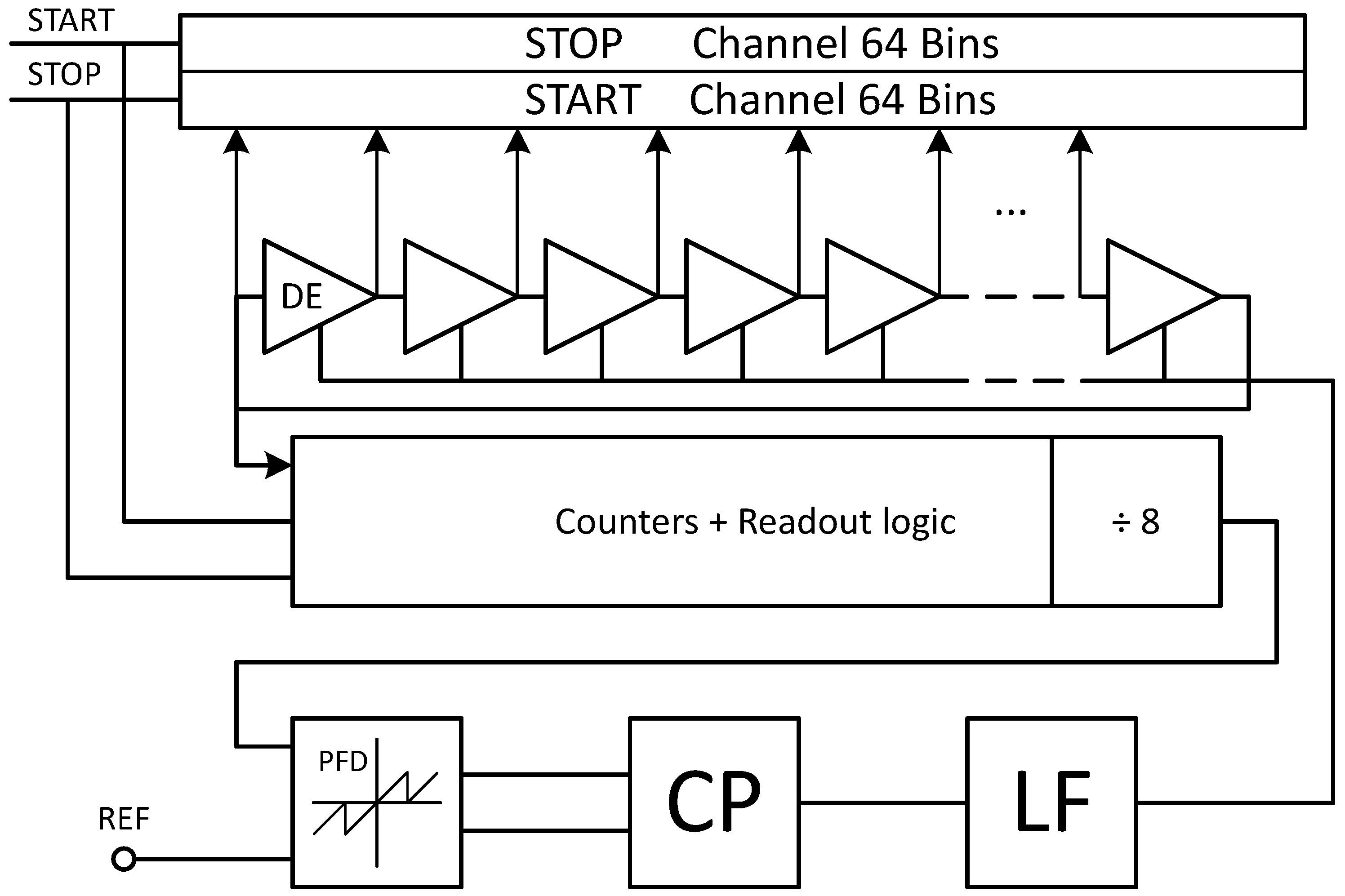
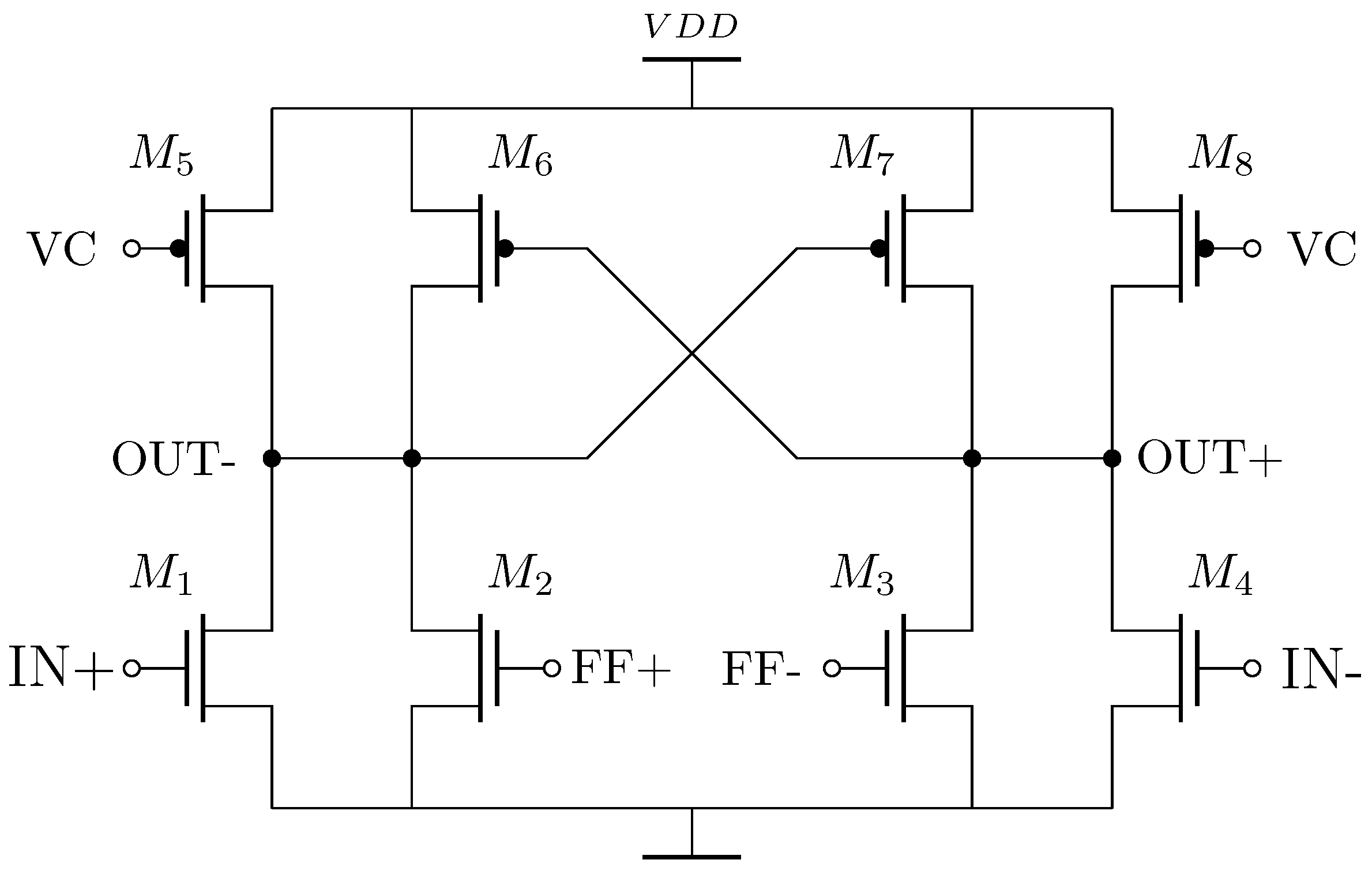
The design presented in this paper is based on a second-order phase locked loop (PLL) with a ring oscillator as voltage controlled oscillator (VCO). Figure 1 shows the VCO which consists of 64 delay cells, based on pseudo differential delay cells [16]. The PLL is locked to a reference clock of with a multiplication factor of 8. The VCO thus runs at a stable frequency of 1 GHz, which leads to a period of 1 ns for the fine detection range. Therefore, once the PLL is locked the average static delay of the delay cells is 15.6 ps. The PLL feedback loop is used to ensure that the TDC is robust against process, voltage and temperature (PVT) variations, and additionally to variations due to ionizing radiation. Ionizing radiation, more specificaly the total ionizing dose (TID), influences the devices by changing the threshold voltage () and degrading the mobility, due to trapped charges in the devices [17]. This change in and mobility will decrease the current consumption of the circuit which leads to decreased performance [18]. In the case of the VCO, the oscillation frequency would decrease. Nevertheless, the PLL will compensate the degradation of the free running oscillation frequency of the VCO with increasing dose to keep the divided output frequency equal to the 125 MHz reference.
The TDC functionality is accomplished by having two sample channels, which sample the state of the VCO independently, these two channels correspond to the respective START and STOP input events. To further increase the dynamic range of the TDC a digital circuit is implemented which contains two counters of 12-bit (one for every channel), which extends the total dynamic range of the TDC to 4 s. The divided feedback clock for the PLL is generated inside this digital circuit to save power. The entire digital block is designed with enclosed layout transistors (ELT) and synthesized with triple modular redundancy (TMR) to improve the resistance against total ionizing dose (TID) and single event effects (SEE) respectively. The entire chip can be configured digitally and read out, which reduces the number of pins drastically.
3. Circuit Implementation
The full TDC consisted of multiple parts: (1) ring oscillator based VCO, (2) phase-frequency detector, (3) charge pump, (4) loop filter, (5) two channels of sampling flip-flops (FF) and a (6) digital control block. In this section, some of these blocks and the implementation will be discussed separately.
3.1. VCO
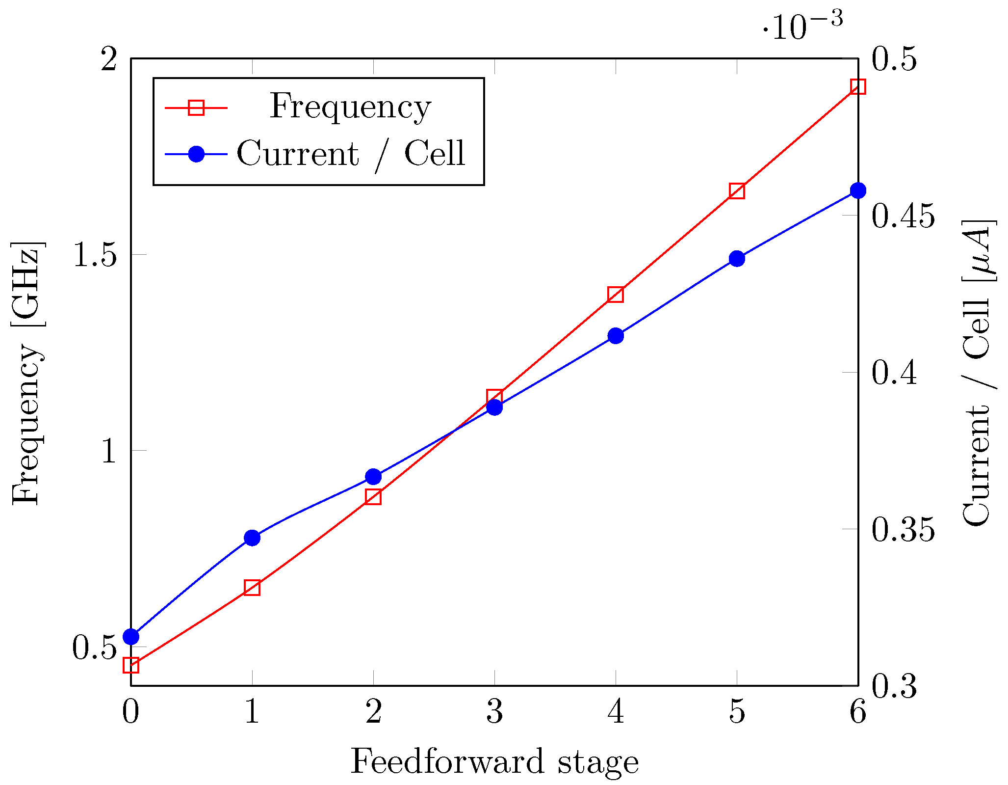
The VCO used in this chip was based on a ring oscillator. The analog tuning of the delay element (DE) was done by changing the gate voltage of the P-type metal-oxide-semiconductor (PMOS) pair M5, M8 (Vc node) which changed the delay of the cell by limiting the current on the rising edge of the DE. The control voltage is inversely proportional to the delay of the DE and can tune the ring oscillator from 600 MHz up to 1.5 GHz. This voltage was controlled by the charge pump (CP) through the loop filter (LF). To reduce the gate delay of the DE, this implementation, has an extra feedforward input to cascade the DE’s using the multipath approach [13], shown in Figure 2. For this ring oscillator, feedforward was foreseen to the third subsequent stage. This made the DE in this oscillator work 2.5 times faster than a ring oscillator without feedforward. Every increase in feedforward stage resulted in a gain of speed as shown in Figure 3. Nevertheless, this implies a serious layout restriction on the amount of stages to connect the feedforward path since routing complexity will increase drastically. Therefore, the feedforward path is only connected to three stages further. The layout of the cell is shown in Figure 4a. The pseudo differential property of the DE helps to have a signal with large voltage swings and steep edges. This decreased the effect of jitter and leads to cleaner sampling of the sense flip-flops (S-FF). The downside of this type of DE was the larger power consumption due to the feedforward path. It can be seen in Figure 3 that increasing the number of stages of the feedforward path, leads to an overall increase of the power consumption of the ring oscillator. This is because the feedforward devices M2 and M3 are drawing current for a longer time before the primairy path (M1, M4) is turned on.
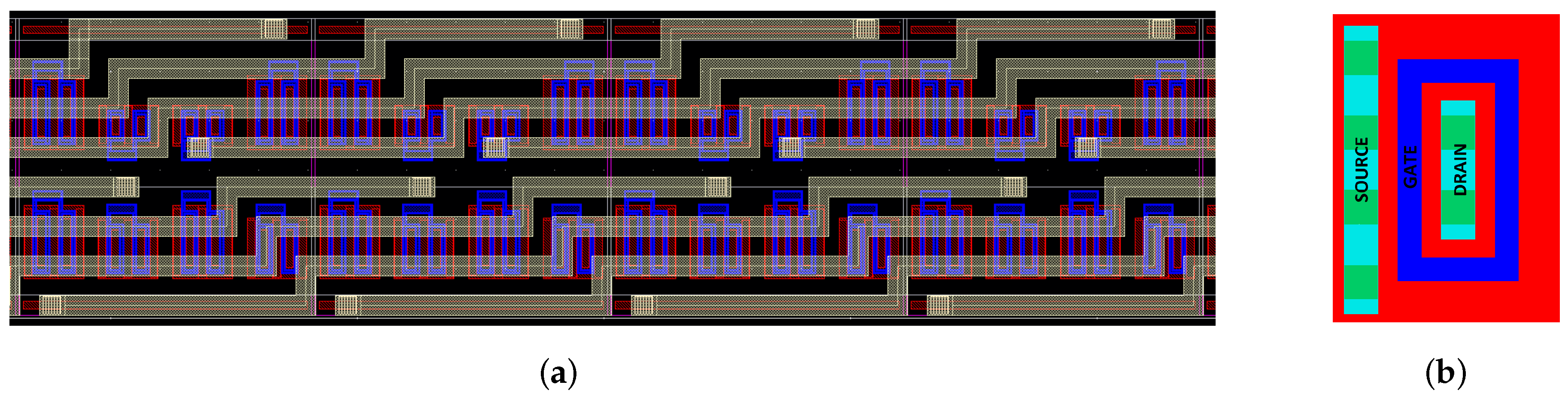
By using 64 stages of the DE as shown in Figure 1, the ring oscillator can easily achieve a frequency of 1 GHz, with a phase noise of −114.3 dBc at 1 MHz shown in Figure 5. The Figure of merit (FOM) is 161.45 dB and did not change with increasing number of feedforward stages. The oscillator had 64 phases which results in a raw resolution of 15.6 ps. The entire ring oscillator was designed with enclosed layout transistors (ELT). This type of transistor has been proven to be more robust against TID effects up to a dose of 10 MGy [19]. ELTs were designed with an enclosed (circular) gate around the drain (Figure 4b). With this technique, the effects of charges captured in the STI were mitigated [20]. A practical restriction of using ELTs was the minimum gate width, which was larger compared to standard transistors because of the physical limitation of the drain contacts, by technology process rules. This also increased the power consumption of the cells.
3.2. Sampling Circuit
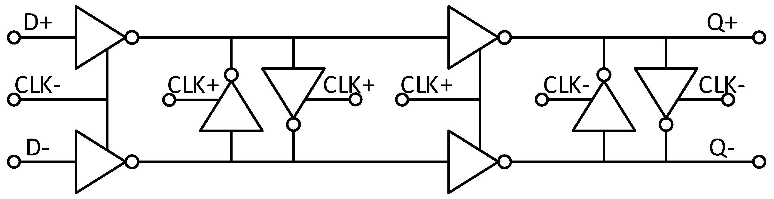
The VCO was sampled by two registers of sense flip-flops (S-FF) to quantize the phase of the ring oscillator. The S-FF was designed using the technique and was implemented in a pseudo differential way. As described in [21], flip-flops contributed significantly in the performance of the TDC due to the influence of the metastability of the flip-flop. The closer the changing input comes to the sampling event, the larger the propagation time. This can lead to bubble forming in the digital code [22]. Therefore, it was necessary to keep the metastable sampling window well below the raw resolution of the TDC. The designed S-FF shown in Figure 6, was therefore used in this design. The circuit consisted of two master–slave edge-triggered flip-flops which are used in a pseudo differential way with inverted cross connections to ensure the static behaviour of the S-FF.
3.3. Digital Control Block
The digital back-end is a fully synthesized logic block which contains the counters to extend the dynamic range beyond the measurement intervals from the ring oscillator which is limited to 1 ns in this design. The digital core is a high-speed digital design which runs at 1 GHz clock speed and is fully triple modular redundant (TMR). This speed is on the edge of commercial 65 nm CMOS ELT cell libraries.
The readout logic saved the 32 bit circular thermometric data from both channels to be read out by the user to further decode the data off-line. The counters, to extend the dynamic range however, required some special attention. One 12 bit, TMR binary counter runs at the 1 GHz input clock coming form the VCO. This counter was incremented on the rising edge of the clock and the value of the counter is sampled by the start- or stop-signal. However, as shown in Figure 7, the output of this counter (C1) was unstable for a period of time after the rising edge of the input clock. This was due to the toggling of the logic. Firstly, if the start- or stop-signals sampled the value when the counter was unstable, the registers can become metastable. Secondly, due to an unknown delay in the registers and mismatch in the clock tree, the time for which C1 was still stable before it toggles was not exactly known. For these two reasons, it was expected that C1 is invalid from the clock edge until it has toggled and is fully stable. To overcome this issue, a second 12 bit register saved the C1 data upon the falling edge of the input clock such that this data is stable when C1 is unstable. Therefore either C1 or C2 will always contain a valid counter value. The selection of either C1 or C2, was based on the decoded 6 bit word coming from the sample registers. The MSB value of the decoded 6 bit word determined the phase of the start- or stop-signal relative to the VCO clock and can determine which counter is stable. For example, if the start signal occurred in the first half period of the VCO clock, the MSB of the fine code will be zero and C2 will be selected. Note that the counter should be constrained such that C1 was stable before half of the clock cycle, which places a constraint of 500 ps in this design. Concerning digital timing, it becomes challenging to meet the timing in the design, especially with respect to TID effects for which an additional timing overhead of 30% is included. The decoding in this design is done in an off-line way. The decoder accepts 32 bits from the start- and stop-register and should find the location on which a 1 to 0 transition occurs in the bit sequence. To overcome SEU errors and single bubbles, a “100” sequence was used to decode the raw TDC data. Finally, after the correct counter value has been selected, both 12 bit and 6 bit words were concatenated and a full time measurement with a dynamic range of s can be performed.
4. Measurement Results
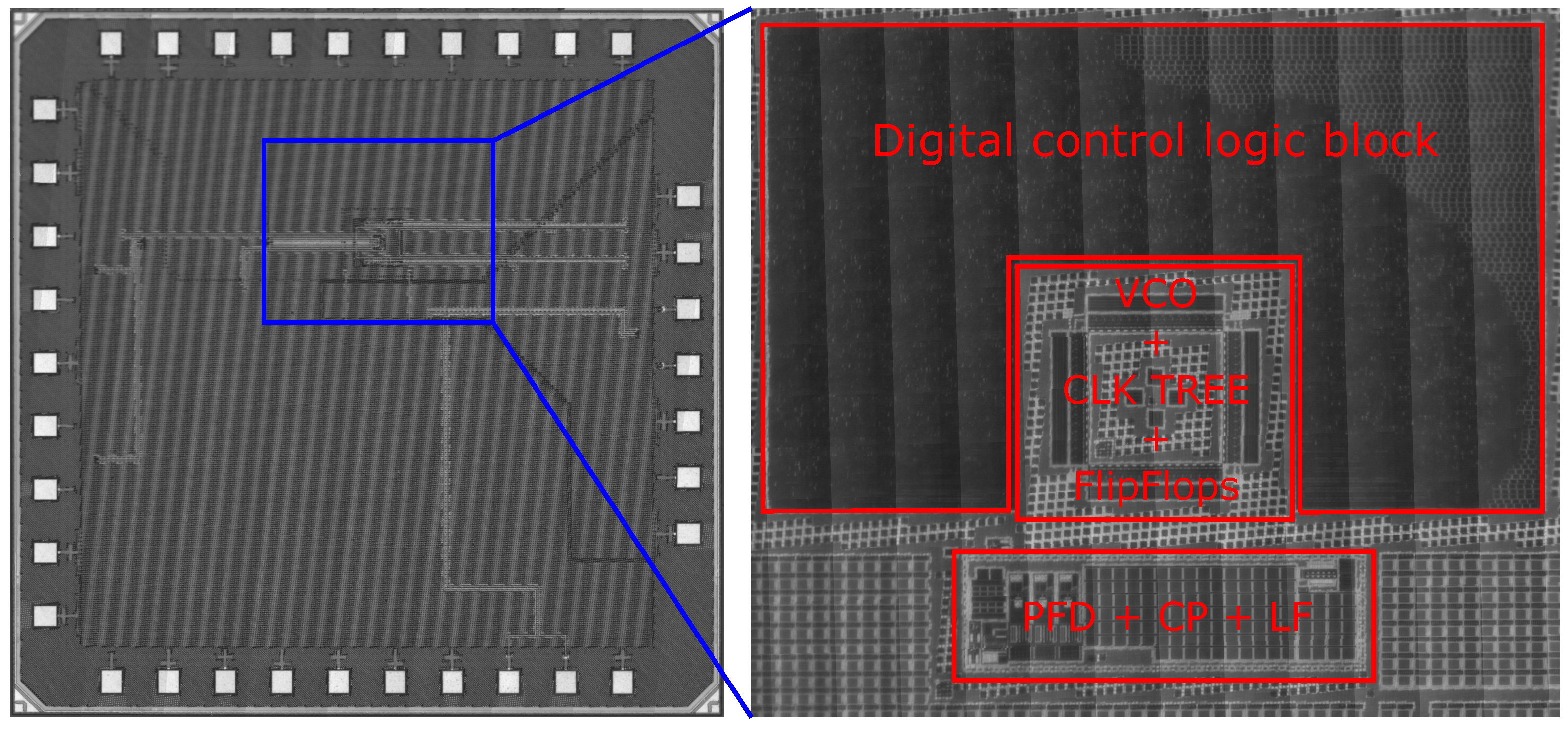
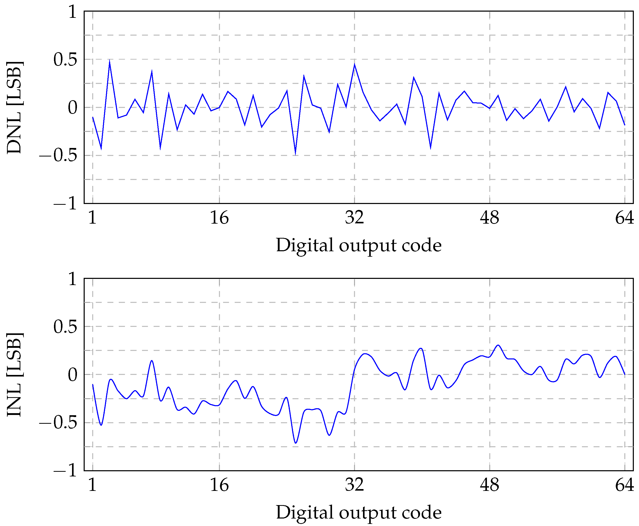
The TDC prototype was manufactured in 65 nm CMOS technology, with a die size of mm. The macro picture is shown in Figure 8. To compare the performance of the chip before and after irradiation, the static INL and DNL were measured by performing a code density test, using a random hit generator which runs completely uncorrelated to the reference clock of the TDC [23]. The measured DNL and INL are shown in Figure 9 and are bound between −0.42/+0.47 LSB and −0.71/+0.30 LSB, respectively.
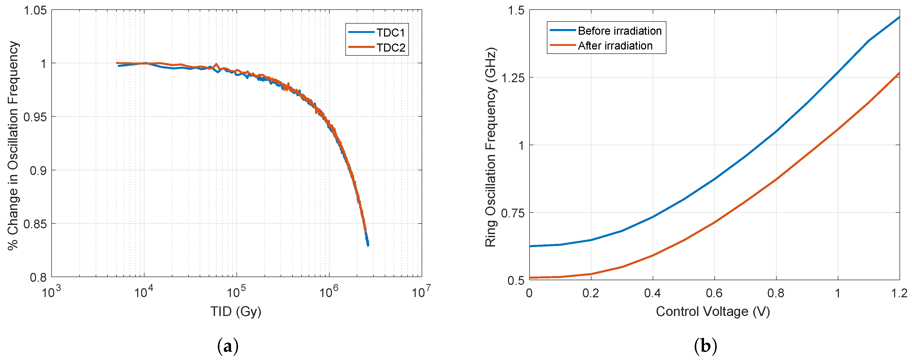
To test the performance of the TDC in terms of TID sensitivity, the TDC was placed under an X-ray beam coming from a 50 keV, 35 mA W-tube from Seifert (Figure 10). This resulted in a dose-rate of 54 kGy/h (). During irradiation, a measurement of the TDC was conducted automatically every five minutes. In this case, there is no interruption of the irradiation which leads to a more precise measurement and more measurement points over time. Two samples were tested, both irradiated up to a dose of 2.5 MGy. During irradiation multiple measurements have been conducted, up to the point where the samples stopped working.
First, a frequency sweep of the open loop ring oscillator was performed to measure the frequency degradation of the ring oscillator. The results of this measurement are shown in Figure 11. Both measured samples only degraded 16% during the complete test. This results in a decreased VCO frequency from 1.5 GHz to 1.25 GHz, which is still more than the targeted frequency of 1 GHz. Therefore, the frequency degradation of the VCO is not the main cause of failing to lock to the phase of the reference signal.
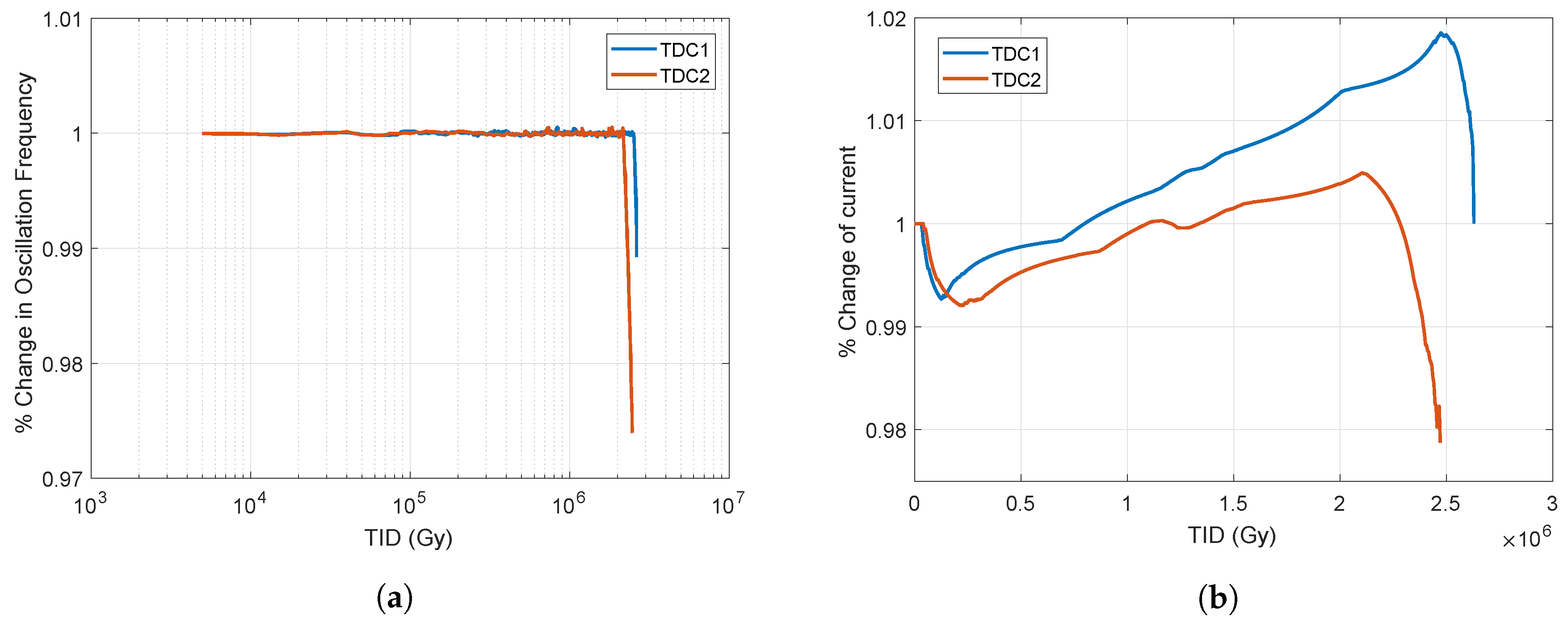
In the second measurement, shown in Figure 12a, the in lock frequency of the PLL was measured. Here, a clear point of failure can be seen for both samples. The first sample reached a dose of 2.17 MGy and the second sample reached a dose of 2.52 MGy. The reason for the loss of lock was originating from the charge pump (CP) controlling the VCO through the loop filter. Although, the CP was designed to initialy deliver an equal up and down current, this also degrades under the influence of ionizing radiation. Known from [24], that PMOS devices degrade more compared to NMOS devices, the CP up and down current drift apart and becomes unbalanced. This combined with a decreasing set point for the VCO due to the decreasing oscillation frequency of the VCO causes the CP and LF to fail delivering the correct control voltage and therefore not able to lock to 1 GHz. Figure 12b, shows the measured current of the TDC while in a locked state. It can be seen that the overall current increased with dose, up to the point where the samples stopped working. To solve the issue of the unbalanced CP, a feedback loop can be implemented. This loop compensates one current source to be equal to the other.
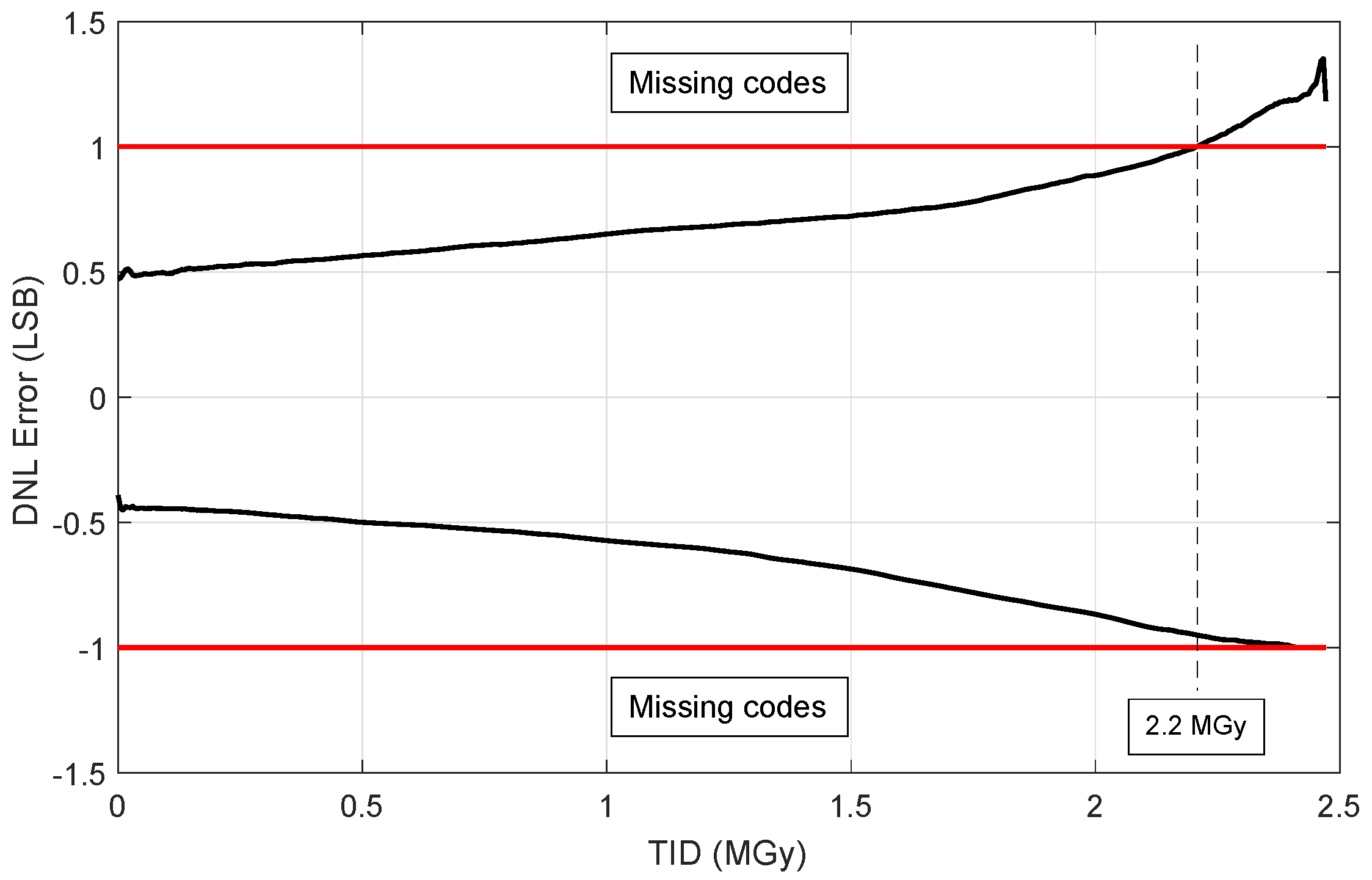
Previous measurements gave an insight in the functional performance of the control loop and showed the point where it fails. The non-linearity of the TDC also gives a clear view of the performance of the TDC. In Figure 9, the INL and DNL of the TDC before irradiation are shown. During irradiation it is clear from Figure 13 that the DNL bounds are expanding with increasing dose. This was as expected since the mismatch between CMOS devices increased with dose [25].
The limit of the DNL error that indicates if the TDC is still performing sufficiently, is . Beyond this point, missing codes can occur. For the measurement shown in Figure 13, this is up 2.2 MGy.
5. Conclusions
This work presents the evaluation of a single-shot TDC in terms of TID. The TDC has a measured resolution of 15.6 ps with a DNL and INL of 0.22 LSB rms and 0.34 LSB rms respectively. Two samples were irradiated and are able to reach a dose of 2.2 MGy before failing to meet specification due to an increased non-linearity error, originating from the increased mismatch in the sampling circuit. The reason for losing the locked state, was found to be originating from the difference in current drift between the up and down currents in the CP. The TDC was fabricated in 65 nm CMOS technology with an active area of 0.312 .
Author Contributions
Conceptualization, B.V.B. and J.P.; methodology, B.V.B. and J.P.; validation, B.V.B.; investigation, B.V.B. and J.P.; writing—original draft preparation, B.V.B., J.P. and P.L.; supervision, J.P. and P.L.
Funding
This research was funded by FWO.
Conflicts of Interest
The authors declare no conflict of interest. The funders had no role in the design of the study; in the collection, analyses, or interpretation of data; in the writing of the manuscript, or in the decision to publish the results.
References
- Hu, C. Future CMOS Scaling and reliability. Proc. IEEE 1993, 81, 682–689. [Google Scholar] [CrossRef]
- Jurgo, M.; Navickas, R. Comparison of TDC parameters in 65 nm and 0.13 μm CMOS. In Proceedings of the 2017 5th IEEE Workshop on Advances in Information, Electronic and Electrical Engineering (AIEEE), Riga, Latvia, 24–25 November 2017; pp. 1–4. [Google Scholar]
- Jee, D.W.; Seo, Y.H.; Park, H.J.; Sim, J.Y. A 2 GHz fractional-N digital PLL with 1b noise shaping Δ Σ TDC. IEEE J. Solid-State Circuits 2012, 47, 875–883. [Google Scholar] [CrossRef]
- Naraghi, S.; Courcy, M.; Flynn, M.P. A 9-bit, 14 μw and 0.06 mm2 pulse position modulation ADC in 90 nm digital CMOS. IEEE J. Solid-State Circuits 2010, 45, 1870–1880. [Google Scholar] [CrossRef]
- Nose, K.; Kajita, M.; Mizuno, M. A 1-ps resolution jitter-measurement macro using interpolated jitter oversampling. IEEE J. Solid-State Circuits 2006, 41, 2911–2920. [Google Scholar] [CrossRef]
- Dudek, P.; Szczepański, S.; Hatfield, J.V. A high-resolution CMOS time-to-digital converter utilizing a Vernier delay line. IEEE J. Solid-State Circuits 2000, 25, 240–247. [Google Scholar] [CrossRef]
- Henzler, S.; Koeppe, S.; Kamp, W.; Mulatz, H.; Schmitt-Landsiedel, D. 90 nm 4.7 ps-Resolution 0.7-LSB single-shot precision and 19 pJ-per-shot local passive interpolation time-to-digital converter with on-chip characterization. In Proceedings of the IEEE International Solid-State Circuits Conference on Digest of Technical Papers, San Francisco, CA, USA, 3–7 February 2008. [Google Scholar]
- Yao, C.; Jonsson, F.; Chen, J.; Zheng, L.R. A high-resolution Time-to-Digital Converter based on parallel delay elements. In Proceedings of the 2012 IEEE International Symposium on Circuits and Systems, Seoul, Korea, 20–23 May 2012; pp. 3158–3161. [Google Scholar]
- Prinzie, J.; Steyaert, M.; Leroux, P. A Self-Calibrated Bang-Bang Phase Detector for Low-Offset Time Signal Processing. IEEE Trans. Circuits Syst. II Express Briefs 2016, 63, 453–457. [Google Scholar] [CrossRef]
- Han, Y.; Rhee, W.; Wang, Z. A PVT-insensitive self-dithered TDC design by utilizing a Δ Σ DLL. In Proceedings of the 2012 IEEE 55th International Midwest Symposium on Circuits and Systems (MWSCAS), Boise, ID, USA, 5–8 August 2012. [Google Scholar]
- Cao, Y.; De Cock, W.; Steyaert, M.; Leroux, P. 1-1-1 MASH Δ Σ time-to-digital converters with 6 ps resolution and third-order noise-shaping. IEEE J. Solid-State Circuits 2012, 47, 2093–2106. [Google Scholar] [CrossRef]
- Gande, M.; Maghari, N.; Oh, T.; Moon, U.K. A 71dB dynamic range third-order Δ Σ TDC using charge-pump. In Proceedings of the IEEE Symposium on VLSI Circuits, Digest of Technical Papers, Honolulu, HI, USA, 13–15 June 2012. [Google Scholar]
- Straayer, M.Z.; Perrott, M.H. A multi-path gated ring oscillator TDC with first-order noise shaping. IEEE J. Solid-State Circuits 2009, 44, 1089–1098. [Google Scholar] [CrossRef]
- Elshazly, A.; Rao, S.; Young, B.; Hanumolu, P.K. A noise-shaping time-to-digital converter using switched-ring oscillators—Analysis, design, and measurement techniques. IEEE J. Solid-State Circuits 2014, 49, 1184–1197. [Google Scholar] [CrossRef]
- Prinzie, J.; Christiansen, J.; Moreira, P.; Steyaert, M.; Leroux, P. Comparison of a 65 nm CMOS ring- and lc-oscillator based PLL in terms of TID and SEU sensitivity. IEEE Trans. Nucl. Sci. 2017, 64, 245–252. [Google Scholar] [CrossRef]
- Moazedi, M.; Abrishamifar, A.; Sodagar, A.M. A highly-linear modified pseudo-differential current starved delay element with wide tuning range. In Proceedings of the 2011 19th Iranian Conference on Electrical Engineering, Tehran, Iran, 17–19 May 2011; p. 1. [Google Scholar]
- Lacoe, R.C. Improving integrated circuit performance through the application of hardness-by-design methodology. IEEE Trans. Nucl. Sci. 2008, 55, 1903–1925. [Google Scholar] [CrossRef]
- Prinzie, J. Radiation Hardened CMOS Integrated Circuits for Time-Based Signal Processing; Springer: Berlin/Heidelberg, Germany, 2017. [Google Scholar]
- Faccio, F.; Michelis, S.; Cornale, D.; Paccagnella, A.; Gerardin, S. Radiation-Induced Short Channel (RISCE) and Narrow Channel (RINCE) Effects in 65 and 130 nm MOSFETs. IEEE Trans. Nucl. Sci. 2015, 62, 2933–2940. [Google Scholar] [CrossRef]
- Johnston, A.H.; Swimm, R.T.; Allen, G.R.; Miyahira, T.F. Total dose effects in CMOS trench isolation regions. IEEE Trans. Nucl. Sci. 2009, 56, 1941–1949. [Google Scholar] [CrossRef]
- Nikolić, B.; Oklobdžija, V.G.; Stojanovič, V.; Jia, W.; Chiu, J.K.S.; Leung, M.M.T. Improved sense-amplifier- based flip-flop: Design and measurements. IEEE J. Solid-State Circuits 2000, 35, 876–884. [Google Scholar] [CrossRef]
- Staszewski, R.B.; Vemulapalli, S.; Vallur, P.; Wallberg, J.; Balsara, P.T. 1.3 V 20 ps Time-to-Digital Converter for Frequency Synthesis in 90-nm CMOS. IEEE Trans. Circuits Syst. II Express Briefs 2006, 53, 220–224. [Google Scholar] [CrossRef]
- Mota, M.; Christiansen, J. High-resolution time interpolator based on a delay locked loop and an RC delay line. IEEE J. Solid-State Circuits 1999, 34, 1360–1366. [Google Scholar] [CrossRef]
- Barnaby, H.J. Total-ionizing-dose effects in modern CMOS technologies. IEEE Trans. Nucl. Sci. 2006, 53, 3103–3121. [Google Scholar] [CrossRef]
- Verbeeck, J.; Leroux, P.; Steyaert, M. Radiation effects upon the mismatch of identically laid out transistor pairs. In Proceedings of the IEEE International Conference on Microelectronic Test Structures, Amsterdam, The Netherlands, 4–7 April 2011. [Google Scholar]
- Hwang, C.S.; Chen, P.; Tsao, H.W. A high-precision time-to-digital converter using a two-level conversion scheme. IEEE Trans. Nucl. Sci. 2004, 51, 1349–1352. [Google Scholar] [CrossRef]
- Yu, J.; Dai, F.F.; Jaeger, R.C. A 12-Bit vernier ring time-to-digital converter in 0.13 μ CMOS technology. IEEE J. Solid-State Circuits 2010, 45, 830–842. [Google Scholar] [CrossRef]
- Lu, P.; Liscidini, A.; Andreani, P. A 3.6 mW, 90 nm CMOS gated-vernier time-to-digital converter with an equivalent resolution of 3.2 ps. IEEE J. Solid-State Circuits 2012, 47, 1626–1635. [Google Scholar] [CrossRef]
- Karadamoglou, K.; Paschalidis, N.P.; Sarris, E.; Stamatopoulos, N.; Kottaras, G.; Paschalidis, V. An 11-bit high-resolution and adjustable-range CMOS time-to-digital converter for space science instruments. IEEE J. Solid-State Circuits 2004, 39, 214–222. [Google Scholar] [CrossRef]
- Christiansen, J. High Performance Time to Digital Converter; CERN Microelectronics Group: Geneva, Switzerland, 2004. [Google Scholar]
Figure 1.
Radiation tolerant single shot time-to-digital converter (TDC) architecture based on a ring oscillator.
Figure 1.
Radiation tolerant single shot time-to-digital converter (TDC) architecture based on a ring oscillator.

Figure 2.
Schematic of the implemented delay element.

Figure 3.
Simulation of the output frequency and power consumption of the ring oscillator with increasing number of feedforward stages.
Figure 3.
Simulation of the output frequency and power consumption of the ring oscillator with increasing number of feedforward stages.

Figure 4.
(a) Layout of the feedforward routing; (b) standard enclosed layout transistors (ELT) layout.
Figure 4.
(a) Layout of the feedforward routing; (b) standard enclosed layout transistors (ELT) layout.

Figure 5.
Simulated phase noise of the ring oscillator with a feedforward path of three stages.
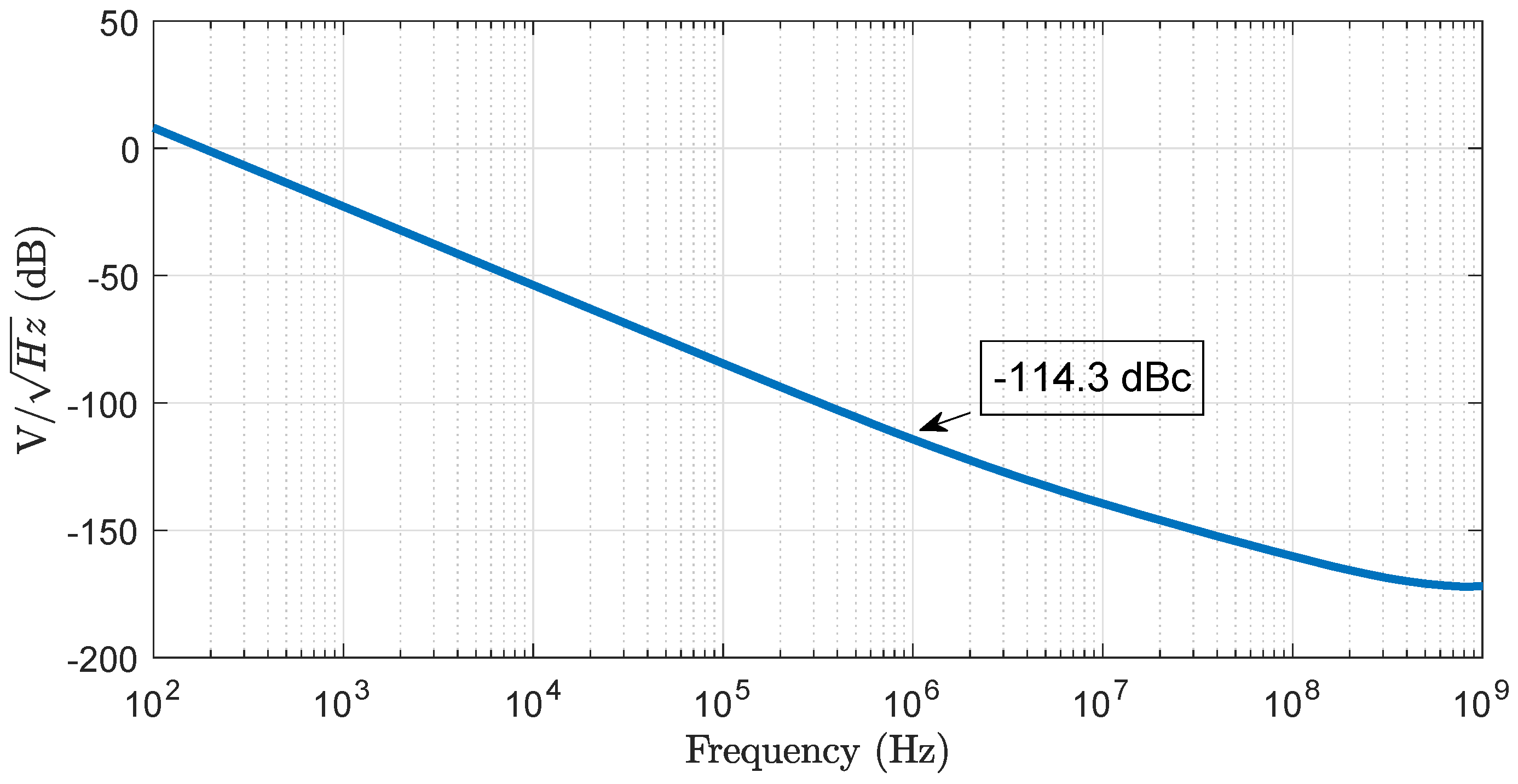
Figure 6.
Schematic of the complementary metal oxide semiconductor () pseudo differential sample flip-flop.
Figure 6.
Schematic of the complementary metal oxide semiconductor () pseudo differential sample flip-flop.

Figure 7.
Stability of the reference counters.
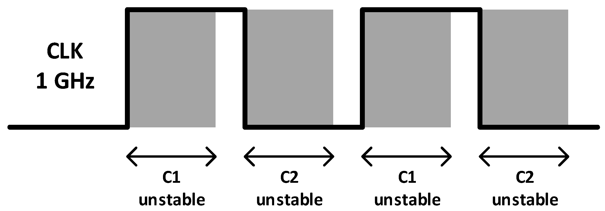
Figure 8.
Photograph of the physical die.

Figure 9.
Measured differential non-linearity (DNL) and integral non-linearity (INL).

Figure 10.
Picture of the used test setup for performing X-ray measurements.
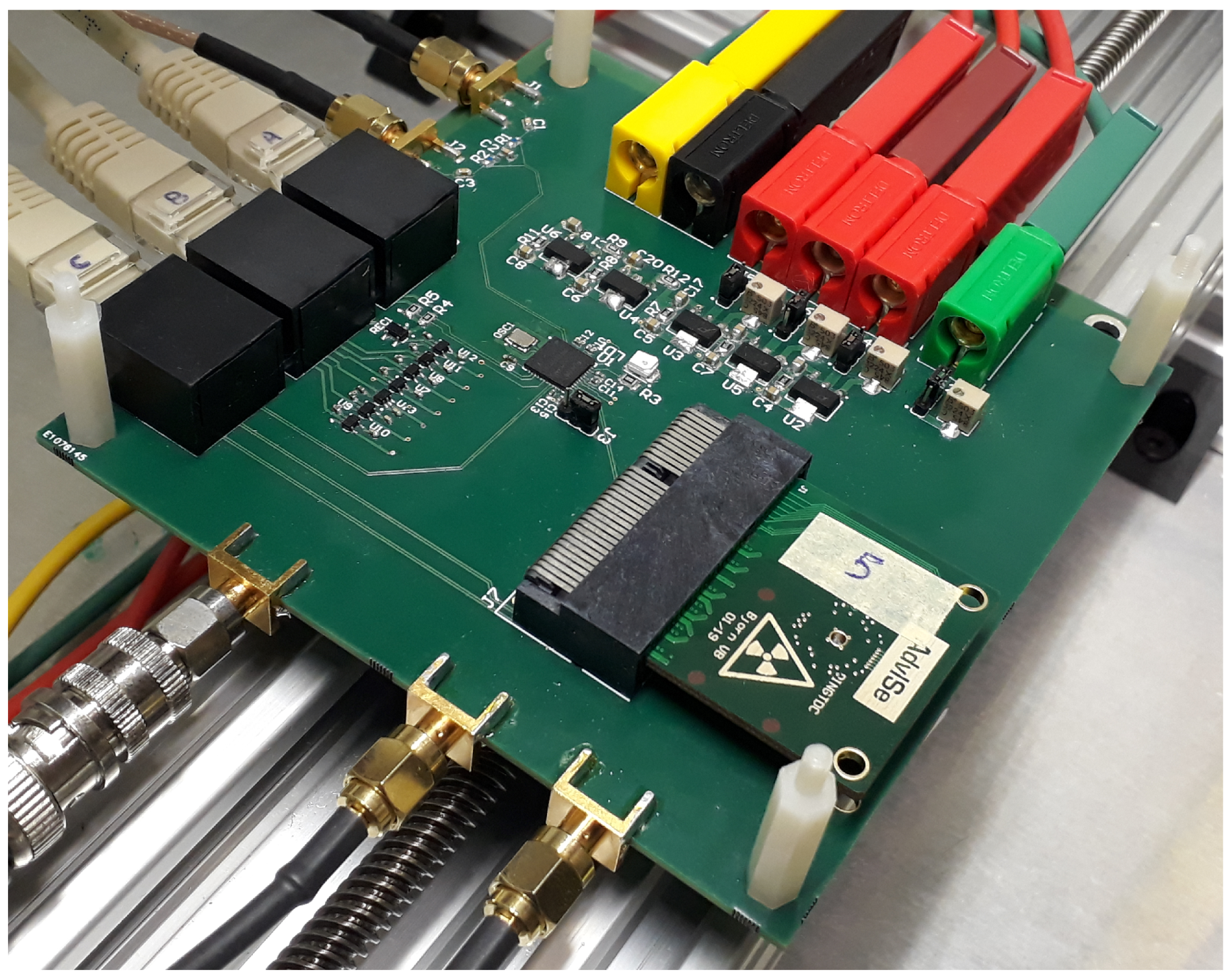
Figure 11.
(a) Frequency degradation of the voltage controlled oscillator (VCO) in open-loop; (b) frequency sweep of the tunable ring oscillator before and after irradiation.
Figure 11.
(a) Frequency degradation of the voltage controlled oscillator (VCO) in open-loop; (b) frequency sweep of the tunable ring oscillator before and after irradiation.

Figure 12.
(a) Frequency degradation of the VCO in closed-loop; (b) percentage degradation of the VCO current.
Figure 12.
(a) Frequency degradation of the VCO in closed-loop; (b) percentage degradation of the VCO current.

Figure 13.
DNL degradation.


Table 1.
Performance summary and comparison.
| Reference | [26] | [27] | [13] | [22] | [28] | This Work |
|---|---|---|---|---|---|---|
| Technology (nm) | 350 | 130 | 130 | 90 | 90 | 65 |
| Technique | 2-level DL | Vernier Ring | GRO | Pseudo Diff | Vernier GRO | Ring |
| Time resolution (ps) | 24 | 8 | 6 | 17–21 | 6.4 | 15.6 |
| Range (bit) | 8 | 12 | 11 | 6 | - | 18 |
| Power (mW) | 50 | 7.5 | 2.2–21 | 6.9 | 4.32 | 134 |
| DNL/INL (LSBrms) | 0.55/1.5 | - | - | 0.7/0.7 | - | 0.22/0.34 |
| Sample rate (MS/s) | 160 | 15 | 50 | 26 | 250 | 200 |
| Area () | 0.6 | 0.26 | 0.04 | 0.01 | 0.027 | 0.26 |
| Radiation Tolerance | - | - | - | - | - | 2.2 MGy |
Table 2.
Performance comparison with related application.
| Reference | [29] | [11] | [30] | This Work |
|---|---|---|---|---|
| Technology (nm) | 800 | 130 | 250 | 65 |
| Technique | Pulse shrinking | DLL | Ring | |
| Application | Space | LIDAR | High Energy Physics | High Energy Physics |
| RAW resolution (ps) | 50 | 10.5 | 24 | 15.6 |
| Range (bit) | 11 | 11 | 21 | 18 |
| Power (mW) | 10 | 1.7 | 450 (multi channel) | 134 |
| DNL/INL (LSBrms) | x/0.45 | - | 0.21/2.1 | 0.22/0.34 |
| Sample rate (MS/s) | 1 | 50 | 8 | 200 |
| Area () | - | 0.11 | - | 0.26 |
| Radiation Tolerance | 1 KGy | 3.4 MGy | 0.3 KGy | 2.2 MGy |
© 2019 by the authors. Licensee MDPI, Basel, Switzerland. This article is an open access article distributed under the terms and conditions of the Creative Commons Attribution (CC BY) license (http://creativecommons.org/licenses/by/4.0/).
Share and Cite
MDPI and ACS Style
Van Bockel, B.; Prinzie, J.; Leroux, P. Radiation Assessment of a 15.6ps Single-Shot Time-to-Digital Converter in Terms of TID. Electronics 2019, 8, 558. https://doi.org/10.3390/electronics8050558
AMA Style
Van Bockel B, Prinzie J, Leroux P. Radiation Assessment of a 15.6ps Single-Shot Time-to-Digital Converter in Terms of TID. Electronics. 2019; 8(5):558. https://doi.org/10.3390/electronics8050558
Chicago/Turabian StyleVan Bockel, Bjorn, Jeffrey Prinzie, and Paul Leroux. 2019. "Radiation Assessment of a 15.6ps Single-Shot Time-to-Digital Converter in Terms of TID" Electronics 8, no. 5: 558. https://doi.org/10.3390/electronics8050558
Note that from the first issue of 2016, this journal uses article numbers instead of page numbers. See further details here.