


A Quadruple Notch UWB Antenna with Decagonal Radiator and Sierpinski Square Fractal Slots


1
Department of Electronics and Communication Engineering, Manipal Institute of Technology, Manipal Academy of Higher Education, Manipal 576104, India
2
Discipline of Electrical, Electronic and Computer Engineering, University of KwaZulu-Natal, Durban 4041, South Africa
3
School of Electronics and Communication Engineering, REVA University, Bengaluru 560064, India
*
Author to whom correspondence should be addressed.
J. Sens. Actuator Netw. 2023, 12(2), 24; https://doi.org/10.3390/jsan12020024
Submission received: 24 February 2023
/
Revised: 7 March 2023
/
Accepted: 11 March 2023
/
Published: 14 March 2023
(This article belongs to the Topic Electronic Communications, IOT and Big Data)
Abstract
:A novel quadruple-notch UWB (ultrawideband) antenna for wireless applications is presented. The antenna consists of a decagonal-shaped radiating part with Sierpinski square fractal slots up to iteration 3. The ground part is truncated and loaded with stubs and slots. Each individual stub at the ground plane creates/controls a particular notch band. Initially, a UWB antenna is designed with the help of truncation at the ground plane. Miniaturization in this design is achieved with the help of Sierpinski square fractal slots. Additionally, these slots help improve the UWB impedance bandwidth. This design is then extended to achieve a quadruple notch by loading the ground with various rectangular-shaped stubs. The final antenna shows the UWB range from 4.21 to 13.92 GHz and notch frequencies at 5.02 GHz (C-band), 7.8 GHz (satellite band), 9.03, and 10.86 GHz (X-band). The simulated and measured results are nearly identical, which shows the efficacy of the proposed design.
1. Introduction
Ultrawideband (UWB) technology has received significant attention in recent years due to its ability to provide high data rates over a large bandwidth [1,2,3]. Because of these unique advantages, UWB technology finds its applications in short-range high-speed communication [4], ranging and monitoring applications [5], the public surveillance domain, and medical imaging [6]. In this context, fractal UWB notch antennas have been extensively researched as compact, low-profile, and high-performance solutions for various wireless communication applications.
Fractals are used in antenna design to create compact antennas with wide bandwidth and the ability to reject specific frequency bands, known as notching. Designing a fractal UWB notch antenna typically involves creating a fractal geometry with the desired electrical characteristics, such as resonant frequency, bandwidth, and return loss [7].
Research has shown that fractal UWB notch antennas can outperform traditional antenna designs in terms of size reduction, bandwidth, return loss, and efficiency. Furthermore, the use of fractal geometry provides a degree of design flexibility, allowing the antenna to be tailored to specific requirements, such as frequency band, polarization, and radiation pattern [7].
Several geometry shapes can be used to design a fractal UWB notch antenna, including a Sierpinski gasket, Koch snowflake, Cantor set, Dragon curve, and Levy C curve [7].
In the literature, many UWB notch antennas have been reported. A hexagonal fractal antenna with improved UWB characteristics was studied in [8]. It uses hexagonal slots and fractal edges, and a U-slot filter was added to reject WLAN-HIPERLAN/2 interference. Another UWB antenna with a dual notch feature was designed in [9] using a combination of an S-shaped slot in the feed line and an L-shaped parasitic structure. In the article [10], a notch antenna was proposed by incorporating a circular slot in the patch to achieve UWB characteristics and create a WLAN band notch. The radiating patch is derived from the circular split ring with two iterations of fractal geometry added.
Another fractal UWB antenna with a dual notch feature was proposed in [11]. The tree fractal structure obtains multi-frequency resonance and UWB operation through increasing iterations and using a defected ground structure, and U-type slots achieve the dual notch band on the tree fractal path. A new compact antenna designed for wireless applications has been introduced in [12]. It features ultrawideband technology, multiple input and output capabilities, and a band-notch feature achieved through additional rectangular stubs. The antenna has two unique monopole elements with a modified T-shaped stub to improve isolation between the radiating elements.
Authors in [13] have proposed a triple-notch UWB antenna using a meander line slot on the radiating patch. In the article [14], using slots, a dual-notch band UWB antenna is proposed. It uses a CPW (coplanar waveguide), defective ground plane, and rectangular radiator to achieve the UWB feature. Authors in [15] have proposed a triple-notch UWB antenna using slots. With modifications to the radiator and a defective ground structure, ultrawideband characteristics are achieved.
A UWB antenna in [16] is designed to achieve a dual-notch using a split ring slot. Modification in rectangular patches helps to achieve wide bandwidth in the UWB range. In the article [17], the authors use an elliptical radiator with a CPW feed along with a slot to achieve UWB characteristics. A circular split-ring resonator and defective ground structure are utilized to achieve triple-notch characteristics. A UWB antenna with quadruple band notch characteristics is designed in [18] using a U-shaped slot and split ring resonator. UWB characteristics are achieved using a combination of half-elliptical patches, triangle patches, and rectangular patches.
Authors in [19] have proposed a fractal UWB antenna with single-band notch characteristics. A hexagonal-shaped patch in the 4th iteration helps get wide bandwidth. A complementary split-ring resonator on the ground plane gives notch characteristics. A UWB fractal antenna is presented in [20,21,22] for rejecting WLAN. It uses CPW feed on a sectorial circular radiator to achieve UWB characteristics. The concept of a programmable metasurface is proposed in [21,22,23] for various wireless applications.
In this article, a fractal Sierpinski square slot with a stub in the ground plane is used to create a quadruple-notch antenna. The fractal structure offers unique advantages such as small size, multiband resonance frequencies, and wider bandwidth. On HFSS, the antenna is developed and simulated. The antenna that was fabricated approved the simulation results. The antenna proposed in this work is based on decagonal Sierpinski UWB fractal antenna presented in [23]. The antenna design approach, parametric analysis, time-domain analysis, and radiation pattern are all covered in the coming section.
2. UWB Antenna Design Approach
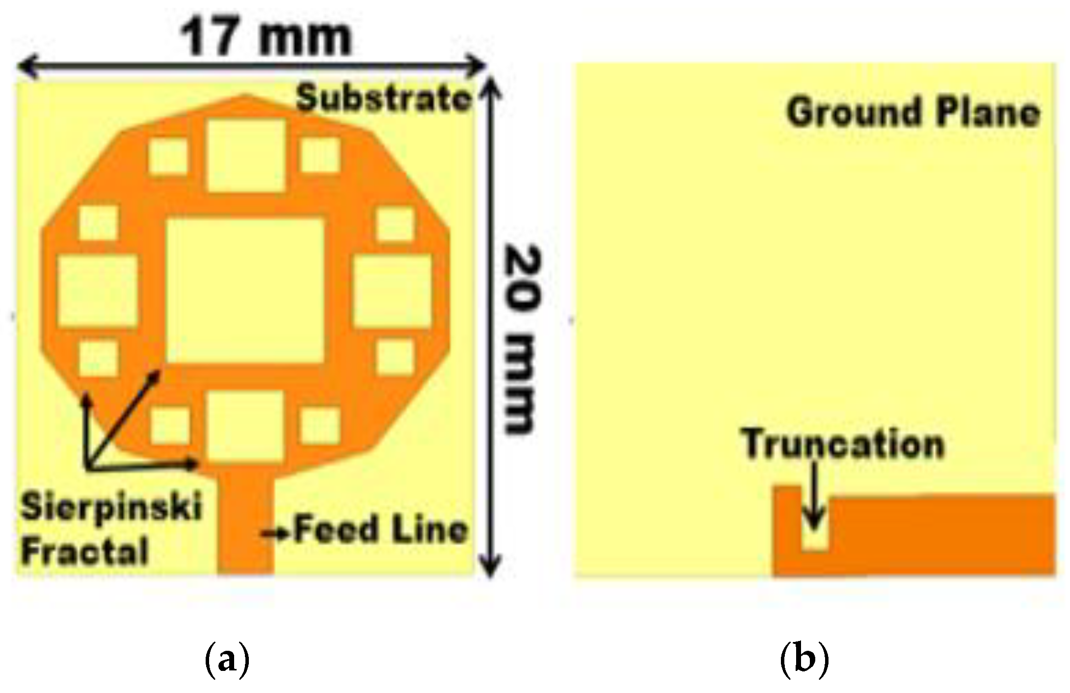
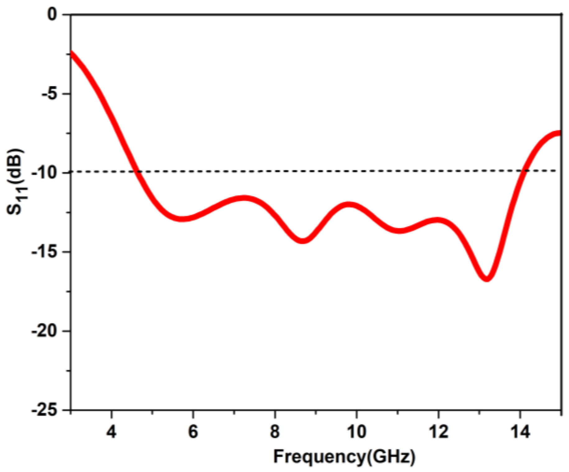
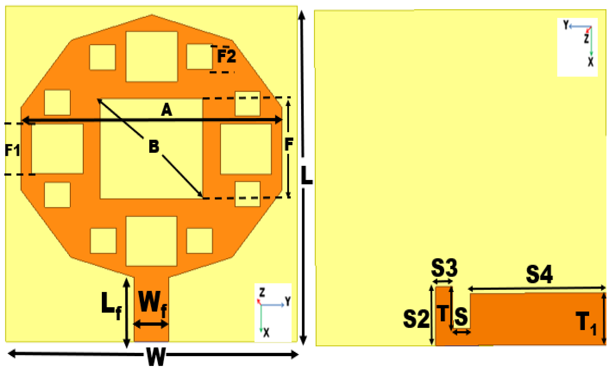
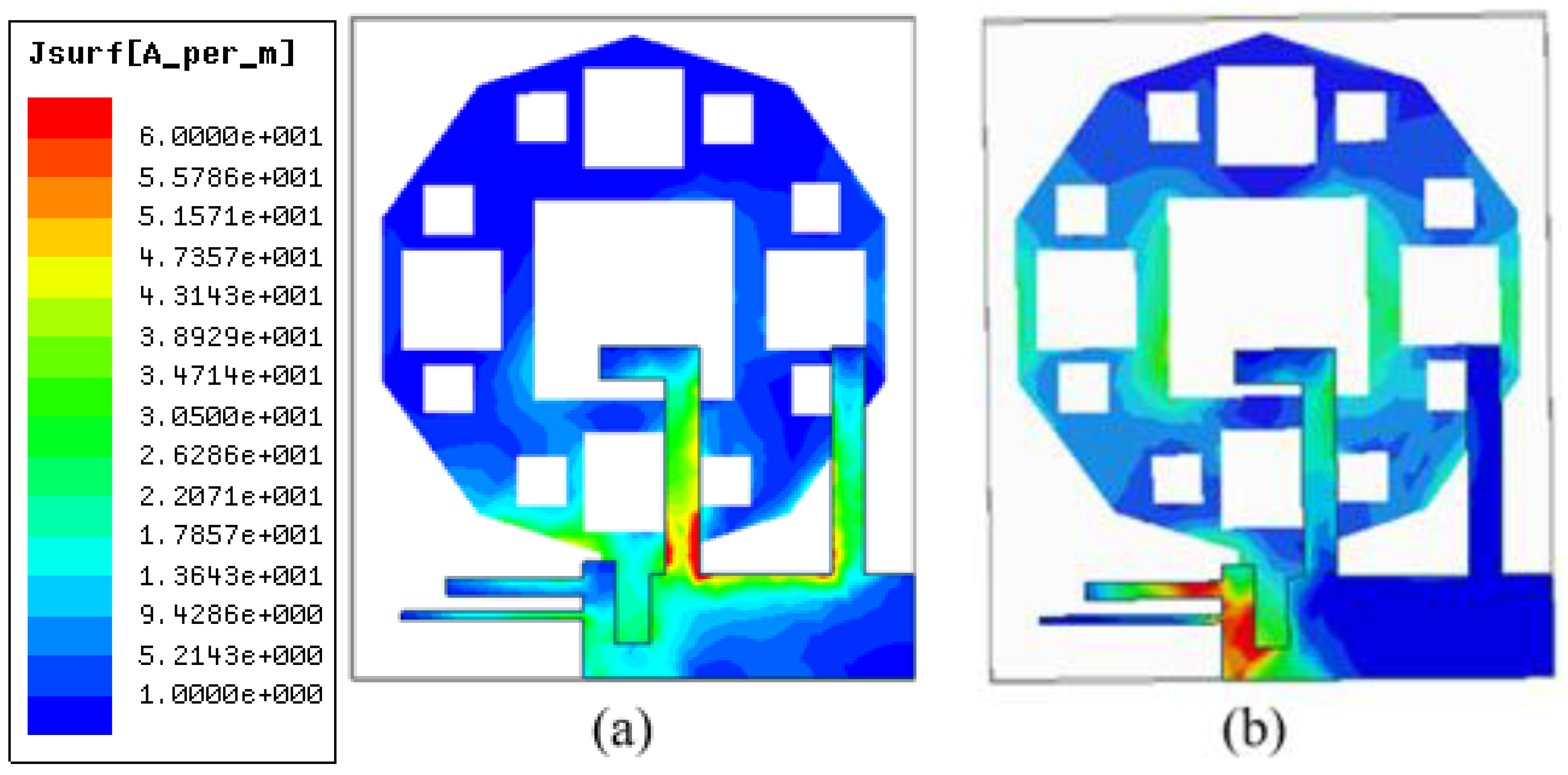
An antenna with a decagonal shape, made up of a radiating patch with Sierpinski square slots and a partial ground plane of 17 × 20 mm2 dimension, has been designed. The addition of Sierpinski square slots affects the antenna’s surface current distribution and changes the input impedance. As shown in Figure 1, this proposed antenna shows excellent UWB characteristics with a reflection coefficient (S11) of less than −10 dB and has a good bandwidth range from 4.64 to 14.14 GHz, as demonstrated in Figure 2. The truncation of the ground plane plays a role in achieving these good UWB properties.
Figure 3 displays the specifications of the proposed antenna, which features Sierpinski square slots on the radiating patch and a truncated ground plane for optimal compactness as a UWB antenna. The impedance match of the microstrip feedline is 50 ohms, and the optimal size is listed in Table 1.
The resonance frequency is calculated using Equations (1)–(3) given below:
By substituting the result of Equation (3) into Equation (2), we obtain
where c stands for the speed of light, which is 3 × 1011 mm/s. A is the width of the patch, B is the diagonal length of the major square at the center, εeff is the effective dielectric constant, h represents the thickness of the substrate, and W represents the substrate’s width.
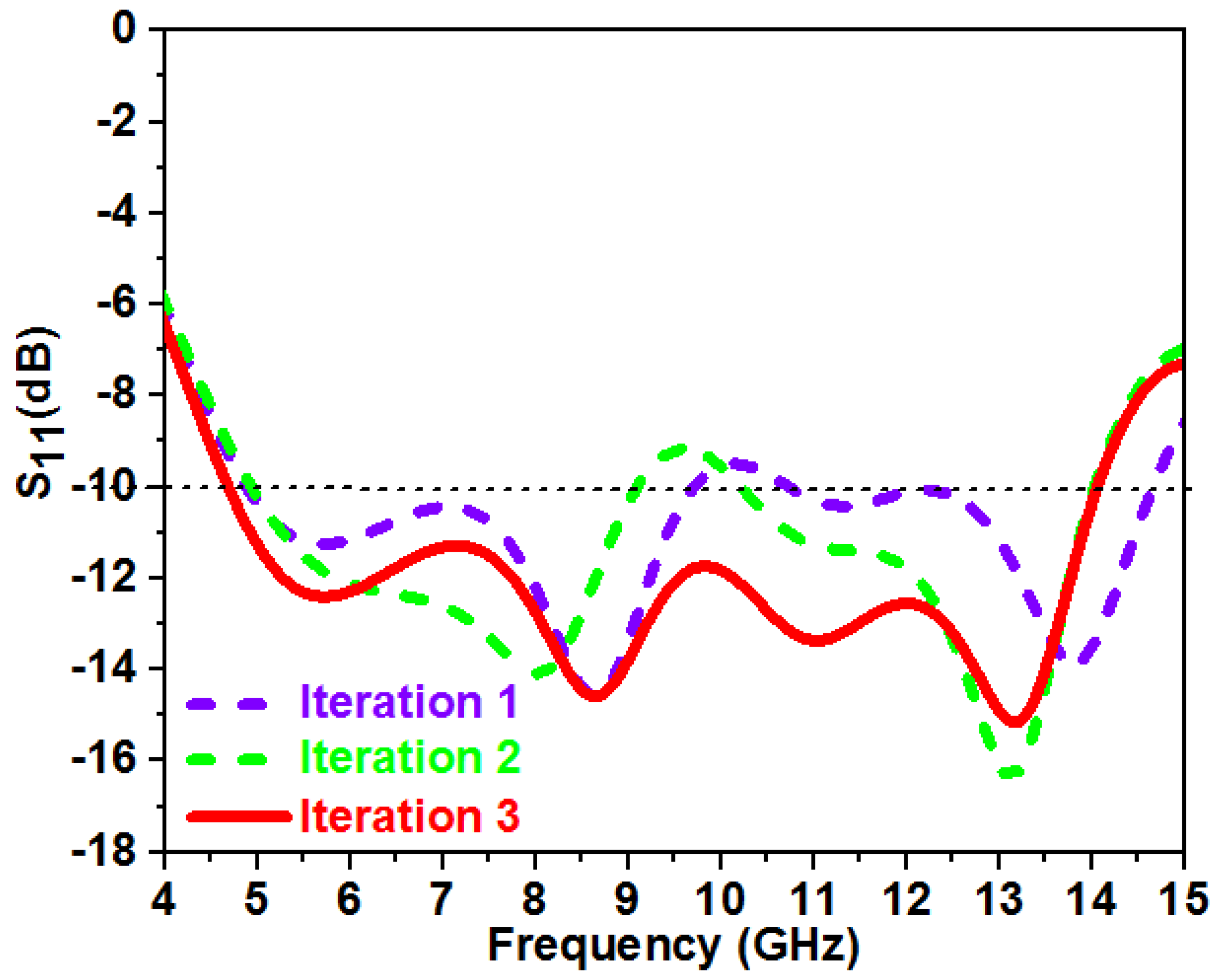
2.1. Progression of UWB Antenna
This section shows the progression of the UWB antenna with respect to fractal change in Figure 4, along with the S11 characteristics in Figure 5.
In iteration 1, a decagonal-shaped radiating patch with a square slot at the center along with a truncated ground plane is designed. However, the S11 value is significantly greater than −10 dB at 10 GHz, and impedance matching is poor. Hence, in iteration 2, the radiating patch was further modified with the introduction of the Sierpinski square slots fractal. As a result, the S11 value is greater than −10 dB at 9.5 GHz, with little improvement in impedance matching. To enhance the result, the Sierpinski square slots fractal was further increased in number on a decagonal-shaped radiating patch in iteration 3. It gives an impedance bandwidth of 4.64–14.14 GHz, covering the UWB range.
2.2. Ground Plane Truncation Effect
The modification process of the ground plane during its development stage is depicted in Figure 6, where the S11 characteristics were graphed for each step. It was observed that iteration C of the proposed antenna had better S11 bandwidth below −10 dB and impedance matching compared to iterations A and B. The results of the S11 analysis are displayed in Figure 7.
2.3. Parametric Analysis
The performance of the antenna design is evaluated through a parametric analysis that looks into the effects of the patch element, the etched slots on the patch, and the ground plane. The factors that influence the design’s outcome are the dimensions T and T1, the width of the feed, and the structure of the ground plane.
2.3.1. Effect of Truncation Length T
The optimal results were achieved when the truncation length T was set to 2.5 mm. The truncation length T was evaluated for different values ranging from 1 mm to 3 mm in increments of 0.5 mm. The results of these simulations were plotted, and it was determined that the best S11 characteristics were obtained at T = 2.5 mm, as depicted in Figure 8.
2.3.2. Effect of Length T1
When the length T1 was set to 3.1 mm, the best results were obtained. The length T1 was tested for several values ranging from 2.8 mm to 3.2 mm in 1.0 mm increments. The results of these simulations were graphed, and the best S11 features were found at T1 = 3.1 mm, as shown in Figure 9.
2.3.3. Effect of Feed Width Wf
The width Wf was tested for several values ranging from 0.5 mm to 2.5 mm in 0.5 mm increments. The results of these simulations were graphed, and the best S11 features were found at Wf = 2.0 mm, as shown in Figure 10.
2.4. Current Distribution
3. UWB Notch Antenna Design
Figure 12 shows the design of the decagonal Sierpinski UWB notch antenna. It can be seen that the radiating part of the conventional UWB antenna is the same. Four stubs—Stub A, Stub B, Stub C, and Stub D—are introduced in the ground part to achieve the notch frequency. Stub A helps in obtaining the notch at 9.1 GHz, while Stubs B, C, and D help in achieving the notch frequency at 4.85, 11.10, and 7.65 GHz, respectively. The corresponding S11 characteristics are plotted and shown in Figure 13.
Figure 14 shows the detailed dimensions of the proposed UWB notch antenna. The optimum design dimensions of the proposed notch antenna are given in Table 2.
3.1. Calculation of the Length of the Individual Stubs and Corresponding Notch Frequency
Calculating the length of the notched band stubs in the ground plane for the UWB notch is as follows:
Length of the stub A
Length of the stub B
Length of the stub C
Length of the stub D
Thus, based on the above calculation, the notch frequency is set. The first notch frequency, , is calculated using Equation (8).
The second notch frequency, , is calculated using Equation (9).
The third notch frequency, , is calculated using Equation (10).
The fourth notch frequency, , is calculated using Equation (11).
3.2. The Development of the UWB Notch Antenna
The evolution stages of the UWB notch antenna are outlined in this section, showcasing the step-by-step process to arrive at the final structure. Figure 15 offers a visual depiction of the iterative journey.
The proposed notch antenna consists of a decagonal Sierpinski square fractal slot, the same as the conventional UWB antenna discussed in Section 2. The ground plane of the conventional UWB antenna is loaded with rectangular stubs to achieve a particular notch frequency. Figure 16 shows a plot of all of the S11 characteristics of the UWB notch antenna at each stage.
In design A, Stub A is added to the ground plane, which gives a notch at 9.1 GHz. In design B, Stub B is added to the ground plane, which gives a notch at 4.85 GHz. After this, in design C, Stub C is added to the ground plane, giving a notch at 11.1 GHz. Finally, in design D, Stub D is added to the ground plane, which gives a notch at 7.65 GHz.
Thus, the combination of four stubs makes the proposed design a decagonal Sierpinski UWB notch antenna. These graphs in Figure 16 show that the notch antenna has S11 < −10 dB for the entire UWB range and has four notches at 4.85, 7.65, 9.1, and 11.1 GHz due to the four stubs.
3.3. Parametric Analysis
Using a parameter-based analysis, the effect of stub dimensions on the performance of a notch antenna is assessed. The dimensions N2, N3, N8, N10, N13, and N15 have a substantial impact on the design’s effectiveness.
3.3.1. Effect of Stub D Width N2
An analysis was conducted to assess the impact of “N2” width on the S11 features. The simulation was performed while varying the width “N2”, and the results are shown in Figure 17. It can be seen that when the width is 0.20 mm, the notch is not adequate. However, when the width is 0.3 mm, the notch S11 curve is near the −10 dB line, leading to poor impedance matching. The best result was obtained with a width of 0.25 mm.
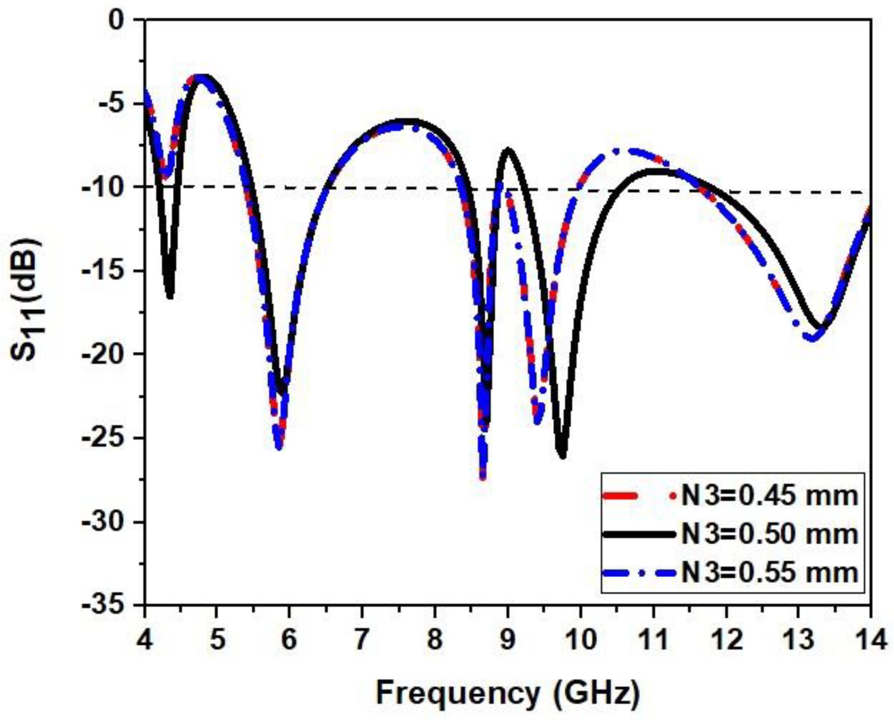
3.3.2. Effect of Stub C Width N3
An analysis was performed to evaluate the impact of width “N3” on the S11 features. The simulation was carried out while changing the width “N3”, and the results are shown in Figure 18. It can be seen that when the width is between 0.45 mm and 0.55 mm, the notch is inadequate. The optimal result was achieved with a width of 0.50 mm.
3.3.3. Effect of Stub C Length N8
The length of the stub C “N8” was simulated and analyzed at N8 = 4.07 mm, N8 = 4.12 mm, and N8 = 4.20 mm. Better results were obtained for a length of 4.12. Hence, for optimal results, 4.12 mm is selected. The result can be observed in Figure 19.
3.3.4. Effect of Stub B Length N10
The length of the stub B “N10” was simulated and analyzed at N10 = 6.4 mm, N10 = 6.9 mm, and N10 = 7.4 mm. Better results were obtained with a length of 6.9. The result can be observed in Figure 20.
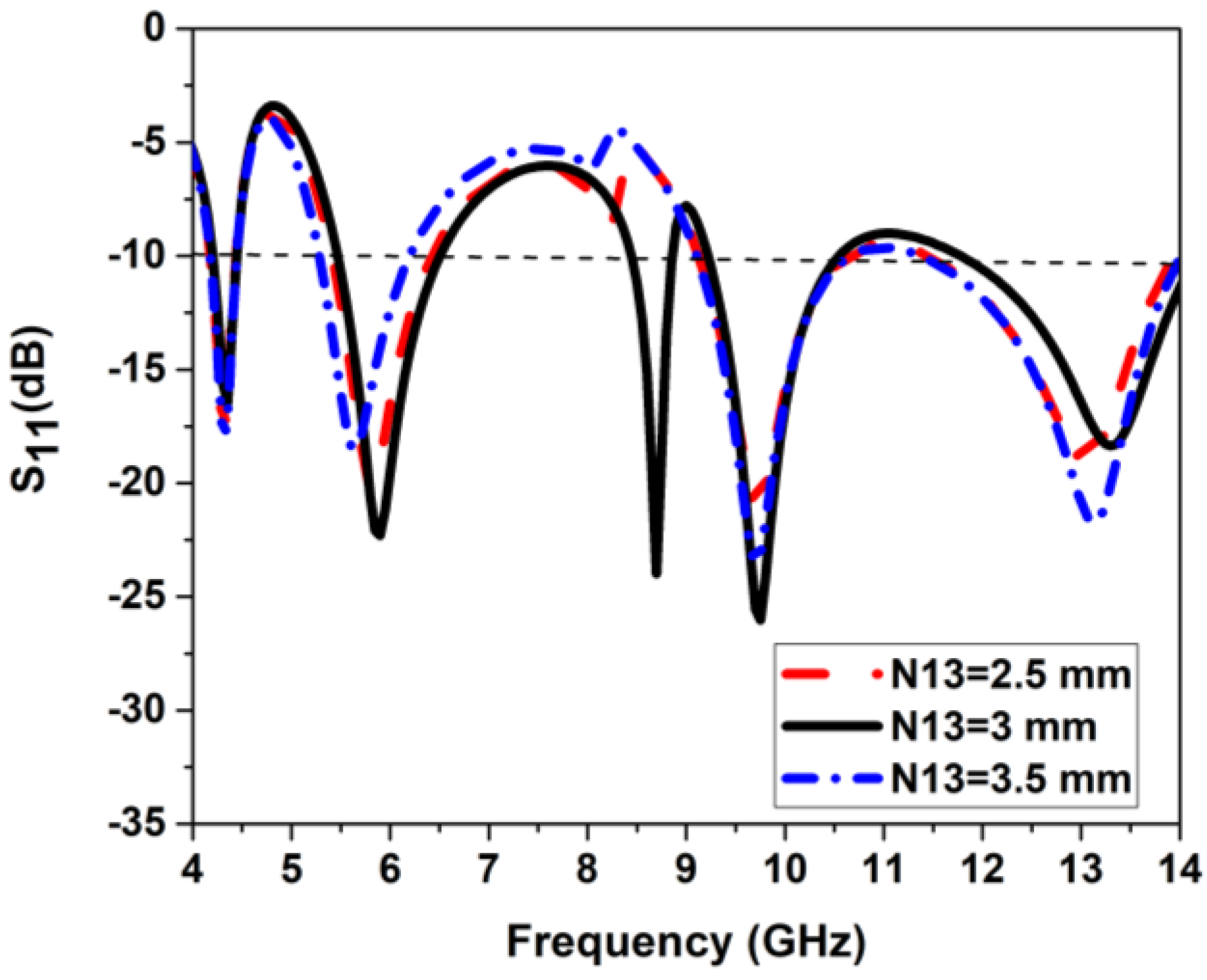
3.3.5. Effect of Stub A Length N13
The length “N13” of stub A was simulated and analyzed at N13 = 2.5 mm, N13 = 3 mm, and N13 = 3.5 mm. Better results were obtained with a length of 3 mm. The result can be observed in Figure 21.
3.3.6. Effect of Stub A Length N15
The length “N15” of stub A was simulated and analyzed at N15 = 6.4 mm, N15 = 6.9 mm, and N15 = 7.4 mm. Better results were obtained with a length of 6.9 mm. The result can be observed in Figure 22.
3.4. Current Distribution at the Operating Frequency of UWB Notch Antenna
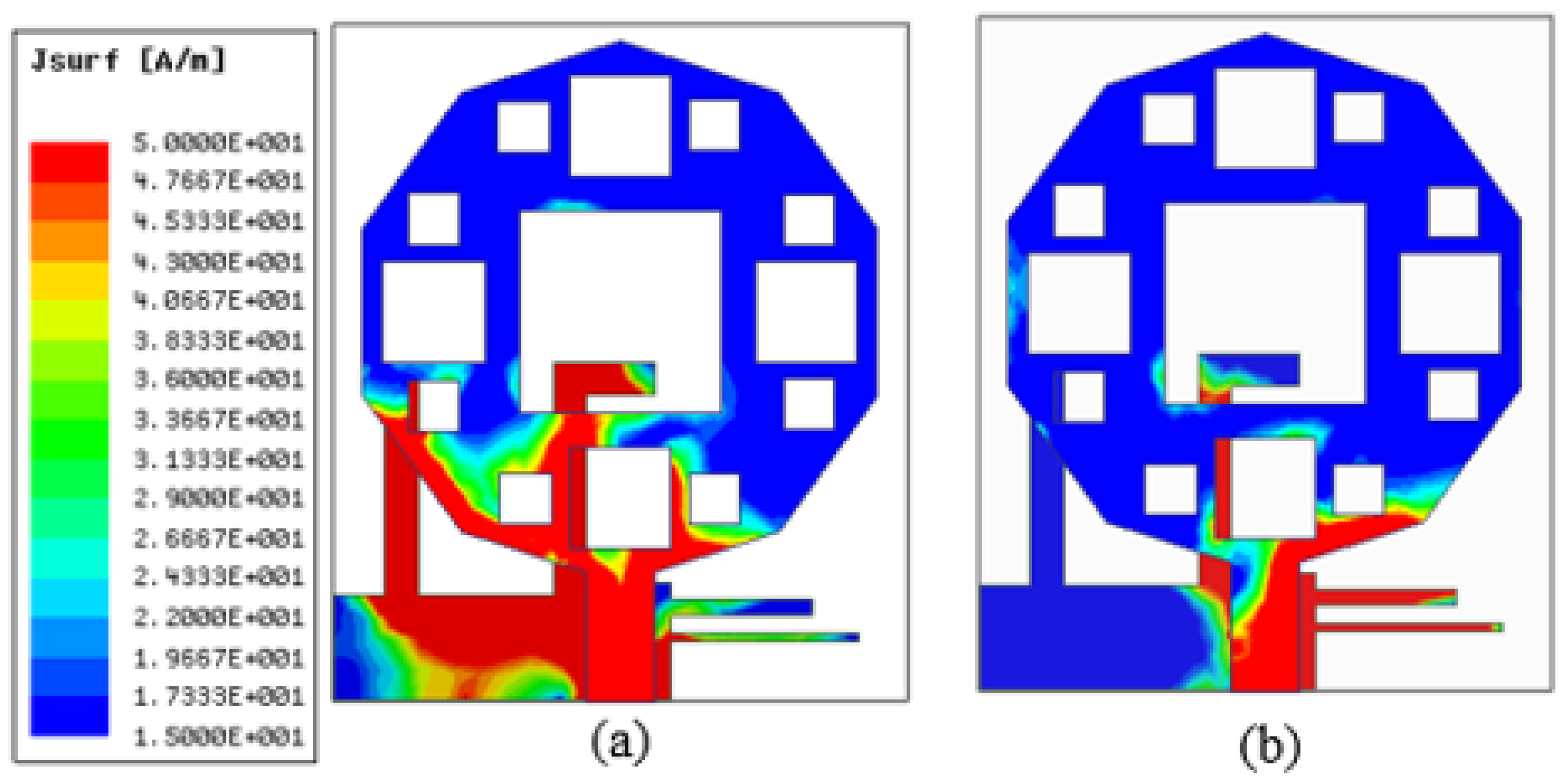
A simulation of the current distribution of the proposed UWB notch antenna was conducted to analyze its performance in Figure 23. The resonance of the antenna was determined at frequencies of 4.35, 5.9, 8.7, and 9.7 GHz. At 4.35 GHz, the highest current was found in the lower left section of the patch and ground plane. At 5.9 GHz, the highest current was located in the lower-right section of the patch and ground plane. The maximum current of 8.7 GHz was observed in the lower middle section of the patch and feed line. At 9.7 GHz, the highest current was seen in the lower half of the patch, feed line, and stubs in the ground plane. The antenna operates using a portion of the C-band at 4.35 GHz, Wi-Fi/WLAN at 5.9 GHz, a portion of the X-band at 8.7 GHz, and a portion of the X-band at 9.7 GHz.
3.5. Current Distribution at Notch Frequency of UWB Notch Antenna
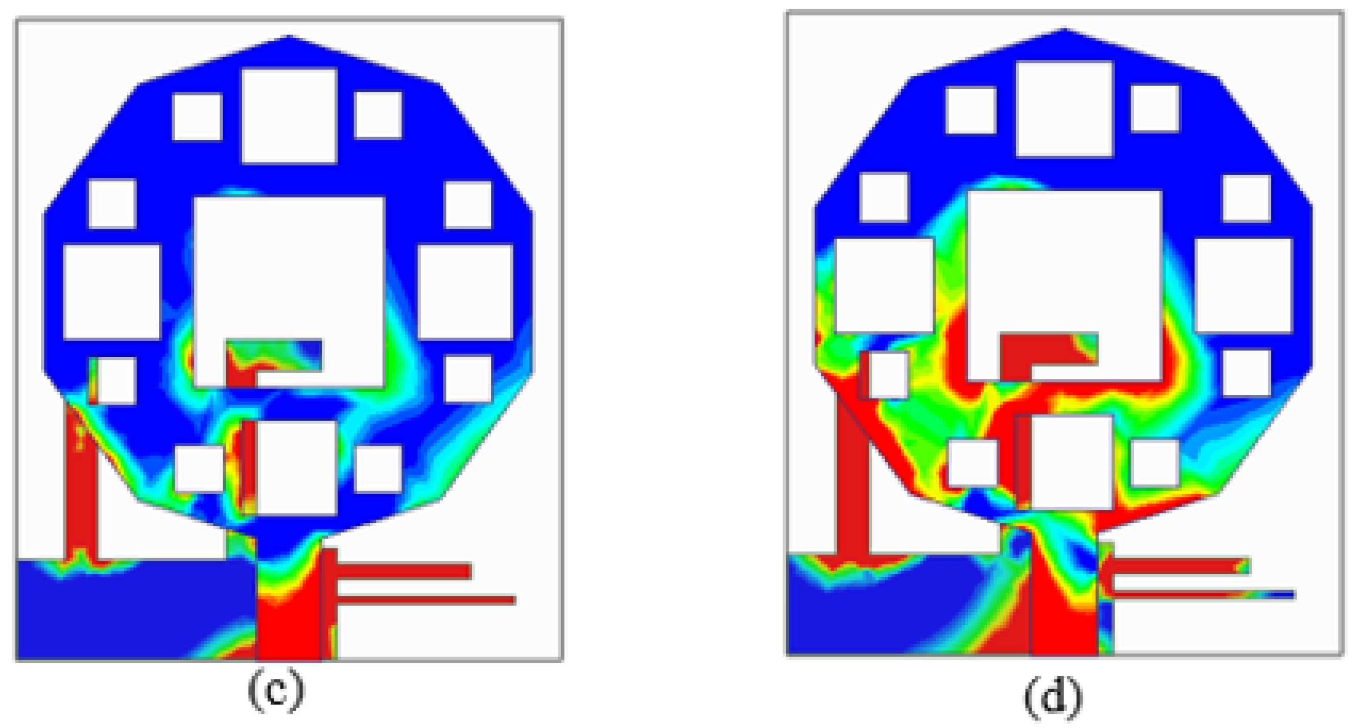
The current distribution is simulated and analyzed, as shown in Figure 24, to realize the operation of the proposed UWB notch antenna at notch frequencies of 4.85, 7.65, 9.1, and 11.1 GHz. The antenna must not radiate at a notch frequency, i.e., the current in the radiating patch should be at a minimum. In Figure 24a–d, it is observed that there is a minimum current around the radiating patch at 4.85, 7.65, 9.1, and 11.1 GHz notch frequencies. The stubs have a more active current due to the notch that is created. It justifies the fact that the antenna is not radiating at these notch frequencies. A portion of the C-band at 4.85 GHz, the satellite band at 7.65 GHz, a portion of the X-band at 9.1 GHz, and a portion of the X-band at 11.1 GHz are rejected by notch antennas.
4. Analysis and Interpretation of Results
The critical steps for the measurement environment of the antenna are simulation, antenna printing, antenna patch curing, measured conductivity, and antenna parameter measurement. Antenna simulation involves using software tools to simulate the behavior of an antenna before it is physically constructed. Antenna printing uses specialized printers to fabricate antennas using conductive ink. Antenna patch curing involves heating the antenna patch to ensure the ink properly adheres to the substrate. Measured conductivity refers to the actual conductivity of the antenna material, which is a critical parameter for determining antenna performance. Antenna parameter measurement involves the process of testing and measuring various antenna parameters such as impedance, radiation pattern, and gain to ensure optimal antenna performance.
4.1. UWB Antenna Results
The suggested antenna was designed and manufactured using the FEM approach on an HFSS simulator. The suggested UWB antenna is shown in Figure 25.
4.1.1. Measured and Simulated S11
Figure 26 contrasts the simulated and measured reflection coefficients. The S11 is measured using a PXI Vector Network Analyzer (300 kHz–14 GHz) from Keysight. The simulated impedance bandwidth is 4.64–14.1 GHz, and the measured impedance bandwidth is 4.75–14.25 GHz. S11 simulations and measurements are nearly identical, with a minor difference. It could be due to the soldering effect, the failure to simulate the SMA connector, errors in the substrate’s dielectric constant, or fabrication tolerances.
4.1.2. Radiation Pattern
4.1.3. Time-Domain Analysis
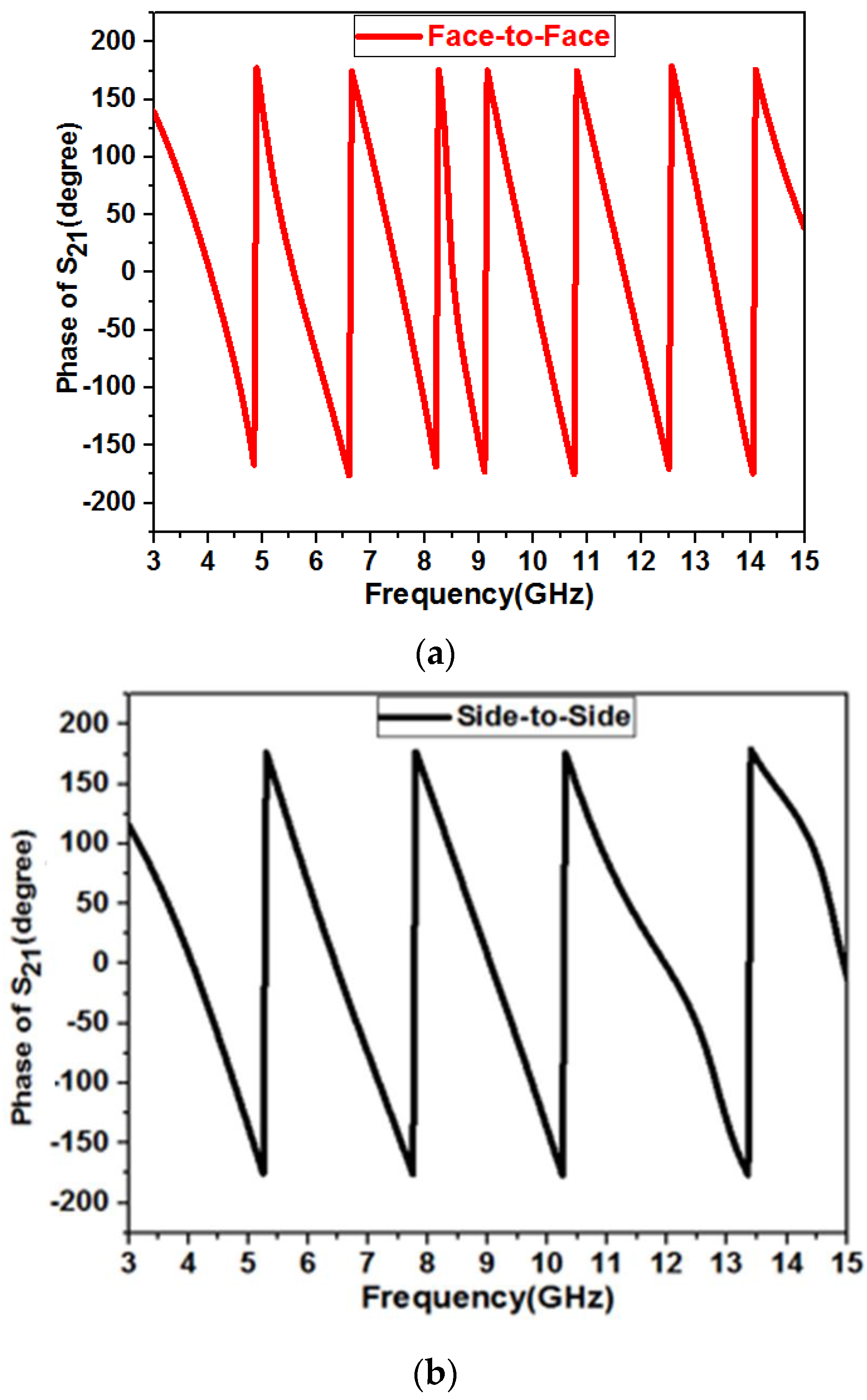
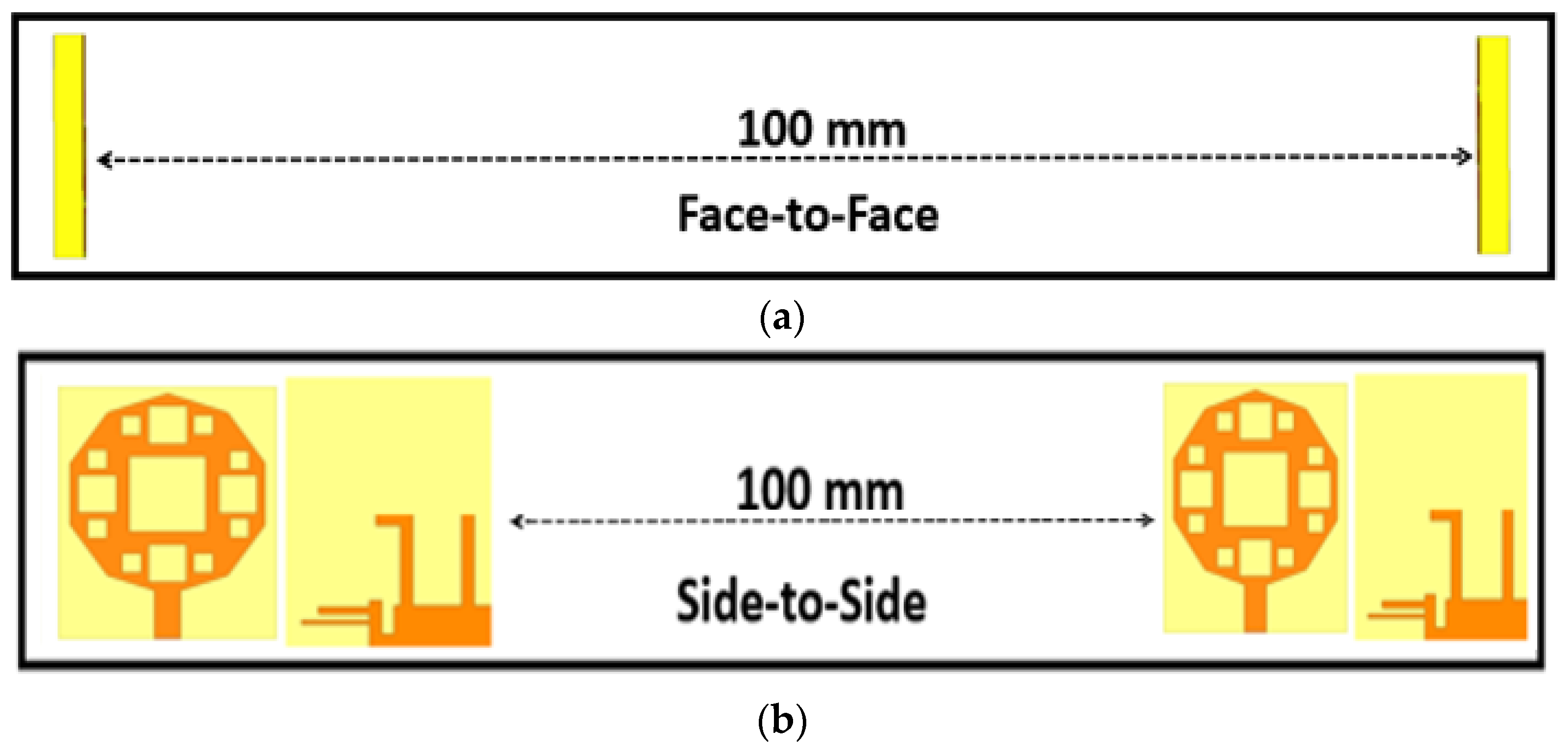
The time-domain analysis, which includes the phase response, the isolation, and the group delay, has already been performed. For the performance study, two identical antennas are placed with a 100-mm spacing in the HFSS software, as illustrated in Figure 28. The time-domain analysis is performed by considering the frontal and lateral conditions.
The group delay, as depicted in Figure 29, is almost linear for both the frontal and lateral conditions of the proposed antenna design.
The isolation characteristics (S21) of the designed UWB antenna are depicted in Figure 30. It is evident that the S21 < −37 dB for the antenna is low in both frontal and lateral conditions.
The phase response as depicted in Figure 31 is almost linear for the antenna in both frontal and lateral conditions.
4.1.4. The UWB Antenna’s Gain
4.2. UWB Notch Antenna Results
The suggested antenna was designed and manufactured using the FEM approach on an HFSS simulator. The suggested UWB notch antenna is shown in Figure 34.
4.2.1. Measured and Simulated S11
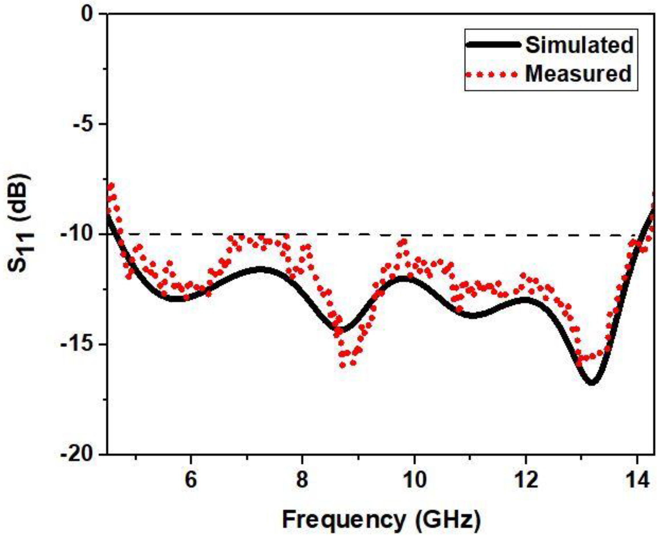
Figure 35 contrasts the simulated and measured reflection coefficients. In the UWB band, both values are nearly identical. The simulated reflection coefficient plot shows that a sharp notch occurs for a portion of the C-band at 4.85 GHz, the satellite band at 7.65 GHz, a portion of the X-band at 9.1 GHz, and a portion of the X-band at 11.1 GHz. The measured reflection coefficient plot shows that a sharp notch occurs for a portion of the C-band at 5.02 GHz, the satellite band at 7.8 GHz, a portion of the X-band at 9.03GHz, and a portion of the X-band at 10.86 GHz. The simulated impedance bandwidth is 4.64–14.1 GHz, and the measured impedance bandwidth is 4.21–13.92 GHz. The green color represents the measured notch, and the yellow color represents the simulated notch of the UWB notch antenna. S11 simulations and measurements are nearly identical, with a minor difference. It could be due to the soldering effect, the failure to simulate the SMA connector, errors in the substrate’s dielectric constant, or fabrication tolerances.
4.2.2. The Radiation Pattern of Notch Antenna at Operating Band
Figure 36 displays the simulation results of the antenna radiation pattern for various frequencies within the operating range. The radiation pattern is omnidirectional in both the E-plane and the H-plane.
4.2.3. Time-Domain Analysis
Phase response and group delay are performed by keeping a 100-mm gap between two antennas, as shown in Figure 37.
Figure 38 shows that the group delay is almost linear for both frontal and lateral orientations, except in the notch bands.
Figure 39 shows that the designed notch antenna has frontal and lateral isolation characteristics that are considered to be acceptable.
The phase response is almost linear for both frontal and lateral orientations except for the notch bands, as shown in Figure 40.
4.2.4. Comparison Table
Table 3 tabulates a comparison of our proposed design with the existing literature. Our design surpasses the current literature based on size, operation, and design complexity.
5. Conclusions
In conclusion, this study presents a novel quadruple-notch UWB antenna design that is suitable for wireless applications. The decagonal-shaped radiating part with Sierpinski square fractal slots, along with the truncated ground part loaded with stubs and slots, makes the antenna compact with improved UWB impedance bandwidth. The final design demonstrates a UWB range from 4.21 to 13.92 GHz with notch frequencies at 5.02 GHz (C-band), 7.8 GHz (satellite band), 9.03 GHz, and 10.86 GHz (X-band). The results from simulation and measurement are in close agreement, demonstrating the effectiveness of the proposed design.
Author Contributions
Conceptualization, O.P.K., T.A., P.K. (Pramod Kumar), P.K. (Pradeep Kumar) and S.B.K.; Methodology, O.P.K., T.A., P.K. (Pradeep Kumar) and S.B.K.; Software, O.P.K.; Validation, O.P.K. and T.A.; Formal analysis, O.P.K. and P.K.; Investigation, O.P.K., T.A. and P.K. (Pramod Kumar); Resources, P.K. (Pramod Kumar), P.K. (Pradeep Kumar) and S.B.K.; Data curation, O.P.K.; Writing—original draft, O.P.K.; Writing—review & editing, T.A., P.K. (Pramod Kumar), P.K. (Pradeep Kumar) and S.B.K.; Visualization, T.A. and S.B.K. Supervision, T.A., P.K. (Pramod Kumar); Project administration, T.A. All authors have read and agreed to the published version of the manuscript.
Funding
This research received no external funding.
Institutional Review Board Statement
Not applicable.
Informed Consent Statement
Not applicable.
Data Availability Statement
Not applicable.
Conflicts of Interest
The authors declare no conflict of interest.
References
- Federal Communications Commission (FCC). Revision of Part 15 of The Commission’s Rules Regarding Ultra-Wideband Transmission Systems. In First Report and Order; ET Docket: Washington, DC, USA, 2002; pp. 98–153. [Google Scholar]
- Kumar, O.P.; Kumar, P.; Ali, T.; Kumar, P.; Vincent, S. Ultrawideband Antennas: Growth and Evolution. Micromachines 2021, 13, 60. [Google Scholar] [CrossRef] [PubMed]
- Kumar, O.P.; Kumar, P.; Ali, T. A Compact Dual-Band Notched UWB Antenna for Wireless Applications. Micromachines 2021, 13, 12. [Google Scholar] [CrossRef]
- Kumar, P.; Pai, M.M.; Ali, T. Ultrawideband antenna in wireless communication: A review and current state of the art. Telecommun. Radio Eng. 2020, 79, 929–942. [Google Scholar] [CrossRef]
- Intrieri, E.; Gigli, G.; Gracchi, T.; Nocentini, M.; Lombardi, L.; Mugnai, F.; Casagli, N. Application of an ultra-wide band sensor-free wireless network for ground monitoring. Eng. Geol. 2018, 238, 1–14. [Google Scholar] [CrossRef]
- Srikanth, B.S.; Gurung, S.B.; Manu, S.; Gowthami GN, S.; Ali, T.; Pathan, S. A slotted UWB monopole antenna with truncated ground plane for breast cancer detection. Alex. Eng. J. 2020, 59, 3767–3780. [Google Scholar]
- Anguera, J.; Andújar, A.; Jayasinghe, J.; Chakravarthy, V.S.; Chowdary PS, R.; Pijoan, J.L.; Cattani, C. Fractal antennas: An historical perspective. Fractal Fract. 2020, 4, 3. [Google Scholar] [CrossRef] [Green Version]
- Benavides, J.B.; Lituma, R.A.; Chasi, P.A.; Guerrero, L.F. A novel modified hexagonal shaped fractal antenna with multi band notch characteristics for UWB applications. In Proceedings of the 2018 IEEE-Aps Topical Conference on Antennas and Propagation in Wireless Communications (AWPC), Colombia, CA, USA, 10–14 September 2018; IEEE: Piscataway, NJ, USA; pp. 830–833. [Google Scholar]
- Devana VK, R.; Satyanarayana, V.; Lakshmi, A.V.; Sukanya, Y.; Kumar, C.M.; Ponnapalli, V.P.; Jagadeesh Babu, K. A novel compact fractal UWB antenna with dual band notched characteristics. Analog. Integr. Circuits Signal Process. 2022, 110, 349–360. [Google Scholar] [CrossRef]
- Garg, R.K.; Nair MV, D.; Singhal, S.; Tomar, R. A new type of compact ultra-wideband planar fractal antenna with WLAN band rejection. Microw. Opt. Technol. Lett. 2020, 62, 2537–2545. [Google Scholar] [CrossRef]
- Hu, Z.; Hu, Y.; Luo, Y.; Xin, W. A novel rectangle tree fractal UWB antenna with dual band notch characteristics. Prog. Electromagn. Res. C 2016, 68, 21–30. [Google Scholar] [CrossRef] [Green Version]
- Bhattacharjee, A.; Karmakar, A.; Saha, A.; Bhattacharya, D. Design of a compact UWB MIMO-diversity antenna incorporating fractal inspired isolation structure with band notch characteristics. Microw. Opt. Technol. Lett. 2021, 63, 2597–2605. [Google Scholar] [CrossRef]
- Kodali, R.R.; Siddaiah, P.; Giriprasad, M.N. Design of Quad Band Operational UWB Antenna with Triple Notch Bands Using Meander Line Slot. Prog. Electromagn. Res. M 2021, 109, 63–73. [Google Scholar]
- Nan, J.; Zhao, J.Y.; Wang, Y. A Compact Dual Notch-Band Frequency Reconfigurable UWB Monopole Antenna. Prog. Electromagn. Res. M 2021, 106, 215–226. [Google Scholar] [CrossRef]
- Bharti, B.K.; Singh, A.K.; Gangwar, R.P.; Verma, R. Frequency and Time Domain Analysis of Triple Band Notched UWB Antenna with Integrated Bluetooth Band. Prog. Electromagn. Res. M 2021, 105, 109–118. [Google Scholar] [CrossRef]
- Kaur, K.; Kumar, A.; Sharma, N. Split Ring Slot Loaded Compact CPW-Fed Printed Monopole Antennas for Ultra-Wideband Applications with Band Notch Characteristics. Prog. Electromagn. Res. C 2021, 110, 39–54. [Google Scholar] [CrossRef]
- Lakrit, S.; Das, S.; Ghosh, S.; Madhav, B.T.P. Compact UWB flexible elliptical CPW-fed antenna with triple notch bands for wireless communications. Int. J. RF Microw. Comput.-Aided Eng. 2020, 30, e22201. [Google Scholar] [CrossRef]
- Chakraborty, M.; Pal, S.; Chattoraj, N. Quad notch UWB antenna using combination of slots and split-ring resonator. Int. J. RF Microw. Comput.-Aided Eng. 2020, 30, e22086. [Google Scholar] [CrossRef]
- Zou, Q.; Jiang, S. A compact flexible fractal ultra-wideband antenna with band notch characteristic. Microw. Opt. Technol. Lett. 2021, 63, 895–901. [Google Scholar] [CrossRef]
- Chen, L.; Ma, Q.; Luo, S.S.; Ye, F.J.; Cui, H.Y.; Cui, T.J. Touch-Programmable Metasurface for Various Electromagnetic Manipulations and Encryptions. Small 2022, 18, 2203871. [Google Scholar] [CrossRef] [PubMed]
- Ma, Q.; Bai, G.D.; Jing, H.B.; Yang, C.; Li, L.; Cui, T.J. Smart metasurface with self-adaptively reprogrammable functions. Light Sci. Appl. 2019, 8, 98. [Google Scholar] [CrossRef] [Green Version]
- Ma, Q.; Gao, W.; Xiao, Q.; Ding, L.; Gao, T.; Zhou, Y.; Cui, T.J. Directly wireless communication of human minds via non-invasive brain-computer-metasurface platform. Elight 2022, 2, 11. [Google Scholar] [CrossRef]
- Ali, T.; Subhash, B.K.; Biradar, R.C. A miniaturized decagonal Sierpinski UWB fractal antenna. Prog. Electromagn. Res. C 2018, 84, 161–174. [Google Scholar]
- Puri, S.C.; Das, S.; Tiary, M.G. UWB monopole antenna with dual-band-notched characteristics. Microw. Opt. Technol. Lett. 2020, 62, 1222–1229. [Google Scholar] [CrossRef]
- Choukiker, Y.K.; Behera, S.K. Modified Sierpinski square fractal antenna covering ultra-wide band application with band notch characteristics. IET Microw. Antennas Propag. 2014, 8, 506–512. [Google Scholar] [CrossRef]
- Gorai, A.; Pal, M.; Ghatak, R. A Compact fractal-shaped antenna for ultrawideband and bluetooth wireless systems with WLAN rejection functionality. IEEE Antennas Wirel. Propag. Lett. 2017, 16, 2163–2166. [Google Scholar] [CrossRef]
- Rahimi, M.; Heydari, S.; Mansouri, Z.; Gandji, N.P.; Zarrabi, F.B. Investigation and design of an ultra-wideband fractal ring antenna for notch applications. Microw. Opt. Technol. Lett. 2016, 58, 1629–1634. [Google Scholar] [CrossRef]
- Lakrit, S.; Das, S.; El Alami, A.; Barad, D.; Mohapatra, S. A compact UWB monopole patch antenna with reconfigurable Band-notched characteristics for Wi-MAX and WLAN applications. AEU-Int. J. Electron. Commun. 2019, 105, 106–115. [Google Scholar] [CrossRef]
- Lin, Y.; Liang, J.; Wu, G.; Xu, Z.; Niu, X. A novel UWB antenna with dual band-notched characteristics. Frequenz 2015, 69, 479–483. [Google Scholar] [CrossRef]
- Yang, B.; Qu, S. A compact integrated Bluetooth UWB dual-band notch antenna for automotive communications. AEU-Int. J. Electron. Commun. 2017, 80, 104–113. [Google Scholar] [CrossRef]
- Mishra, G.; Sahu, S. Compact circular patch UWB antenna with WLAN band notch characteristics. Microw. Opt. Technol. Lett. 2016, 58, 1068–1073. [Google Scholar] [CrossRef]
- Zarrabi, F.B.; Mansouri, Z.; Gandji, N.P.; Kuhestani, H. Triple-notch UWB monopole antenna with fractal Koch and T-shaped stub. AEU-Int. J. Electron. Commun. 2016, 70, 64–69. [Google Scholar] [CrossRef]
- Gao, G.; He, L.; Hu, B.; Cong, X. Novel dual band-notched UWB antenna with T-shaped slot and CSRR structure. Microw. Opt. Technol. Lett. 2015, 57, 1584–1590. [Google Scholar] [CrossRef]
- Kumar, A.L.; Ranjan, A.; Chauhan, M.; Killamsetty, V.K.; Mukherjee, B. Circular SRR shaped UWB antenna with WiMAX band notch characteristics. In Proceedings of the 2018 IEEE Radio and Antenna Days of the Indian Ocean (RADIO), Wolmar, Mauritius, 15–18 October 2018; IEEE: Piscataway, NJ, USA; pp. 1–2. [Google Scholar]
Figure 1.
Top plane (a) and ground plane (b) of the proposed UWB antenna.

Figure 2.
S11 features of the designed UWB antenna.

Figure 3.
Antenna geometry for ultrawideband.

Figure 4.
Progression stages of UWB antenna.
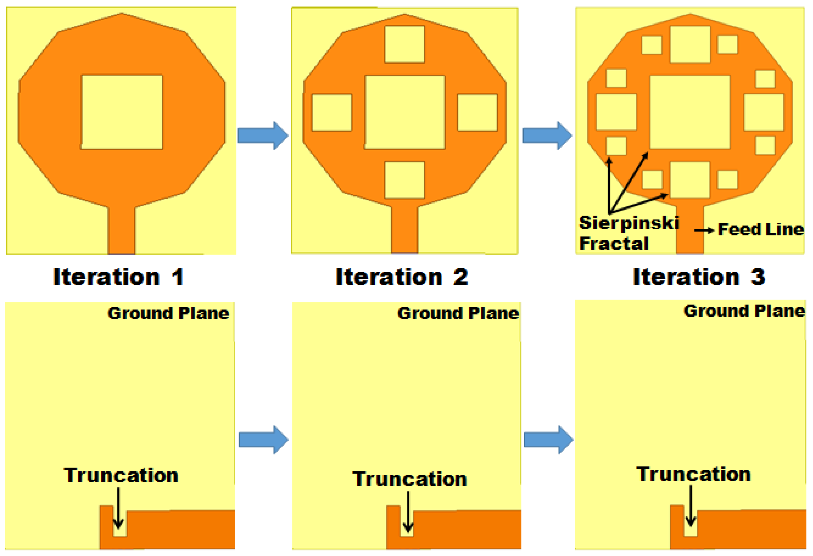
Figure 5.
S11 features of the evolution stages.

Figure 6.
Different iterations of ground plane truncation.

Figure 7.
S11 features of ground plane truncations.

Figure 8.
Parametric analysis for variation in T for S11.
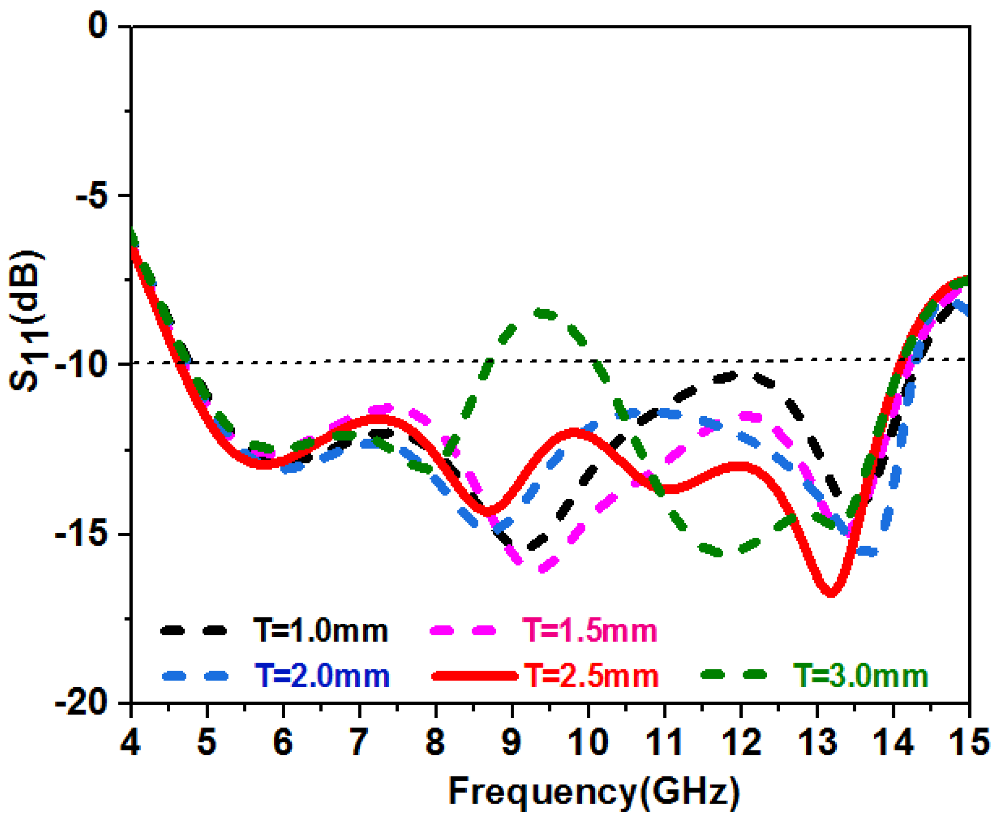
Figure 9.
Parametric analysis for variation in T1 for S11.

Figure 10.
Parametric analysis for variation in Wf for S11.
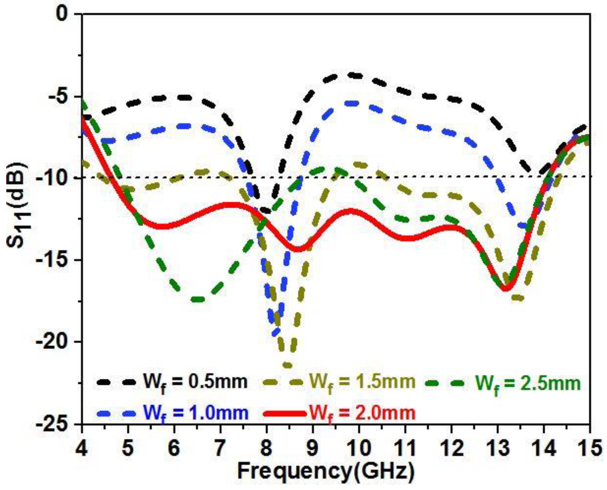
Figure 11.
Surface current at (a) 5.8 GHz, (b) 8.7 GHz, (c) 10.9 GHz, (d) 13.2 GHz.
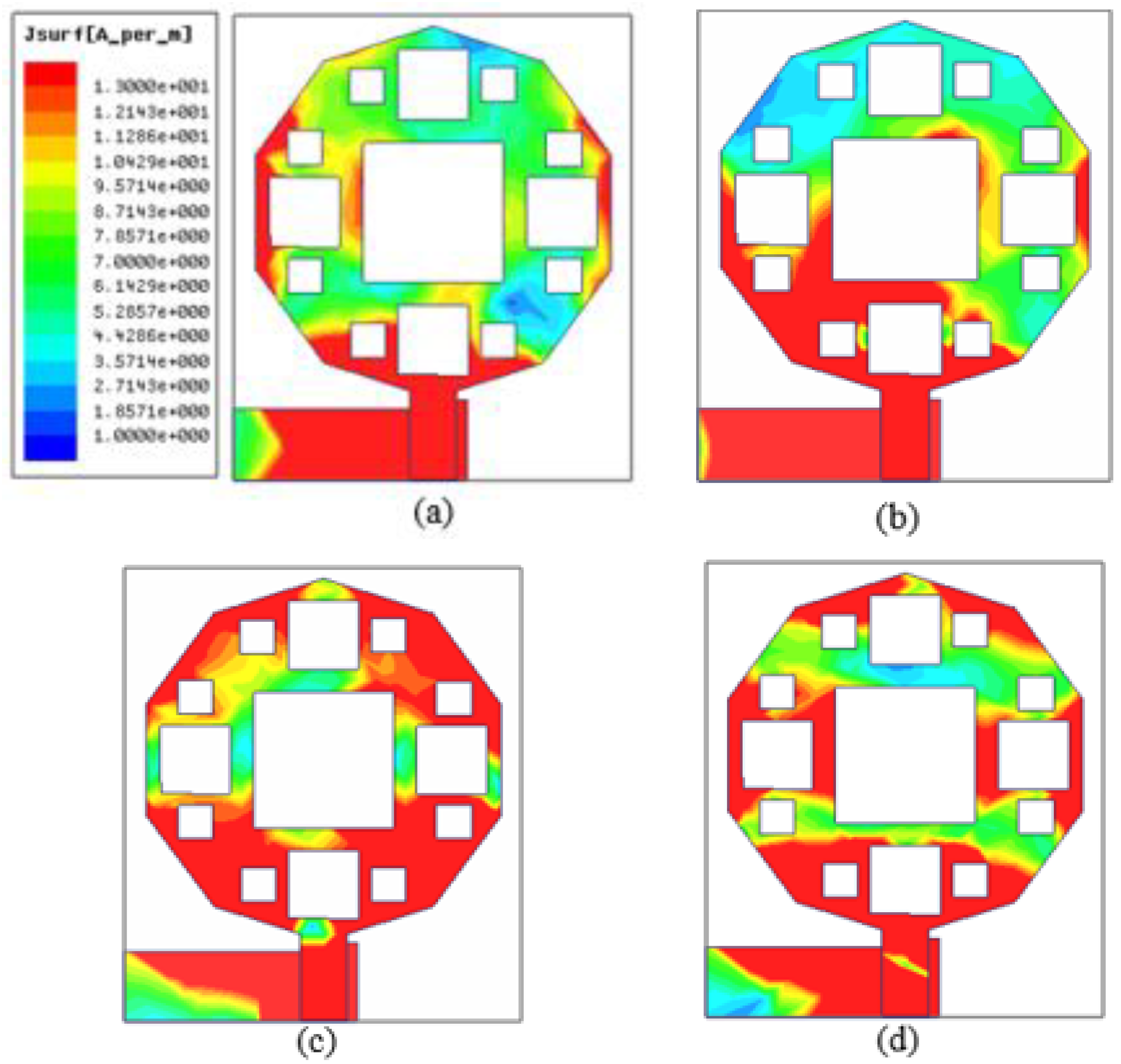
Figure 12.
Front (a) and rear (b) view of Decagonal Sierpinski fractal antenna.
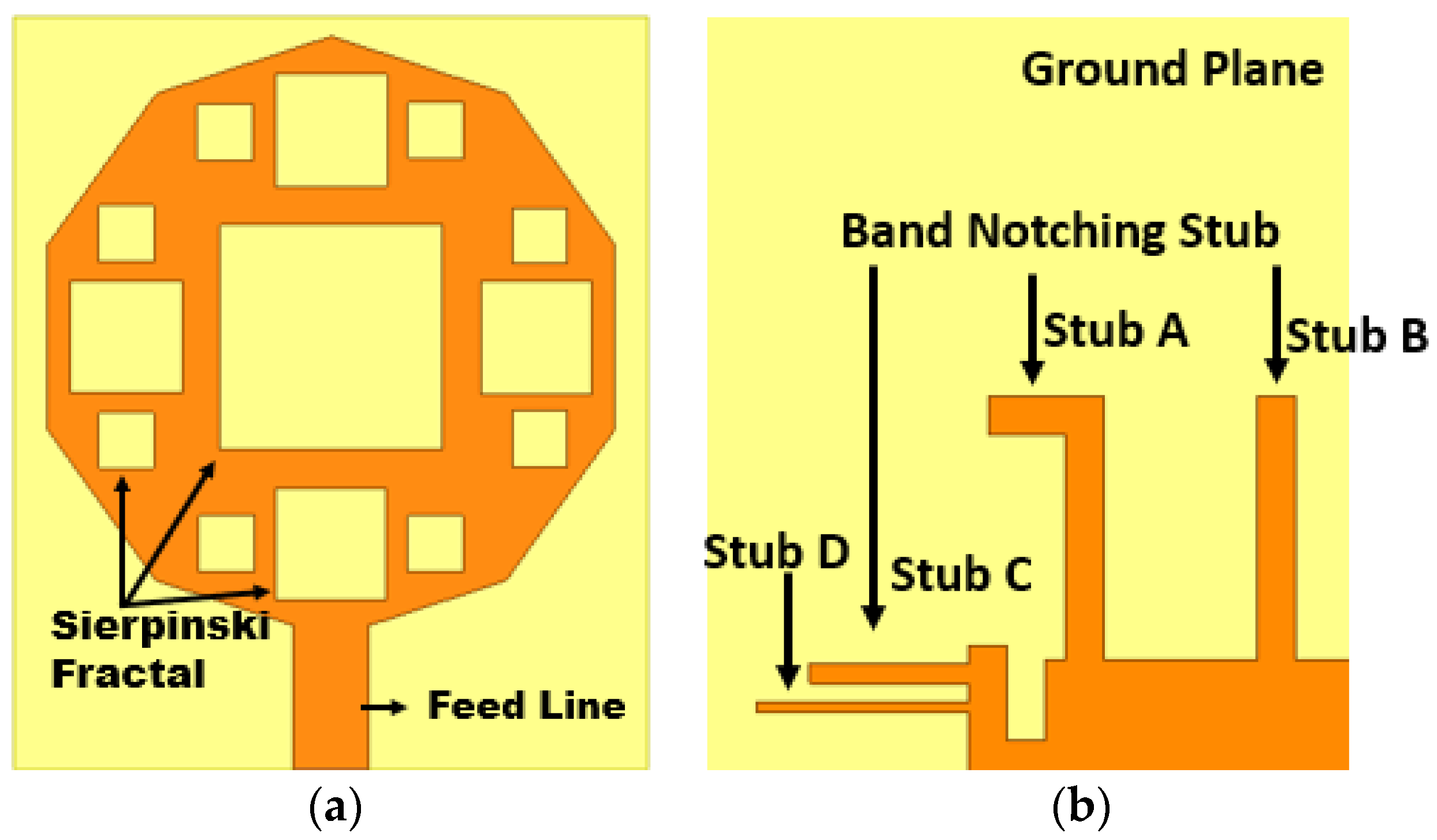
Figure 13.
UWB notch antenna S11 features.

Figure 14.
Detailed layout.

Figure 15.
Progression stages.

Figure 16.
S11 features of the progression stages.
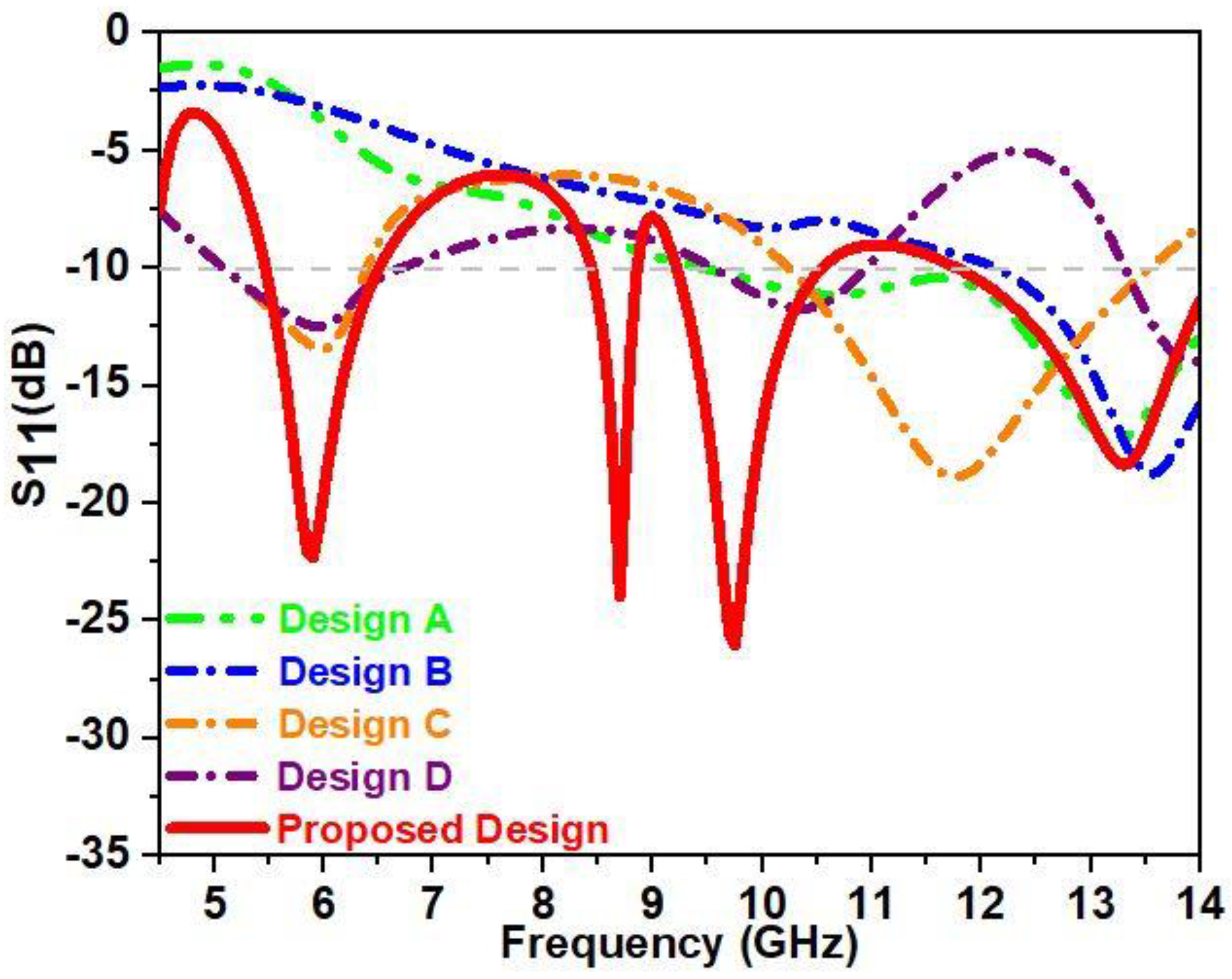
Figure 17.
Parametric analysis for variation in N2 for S11.
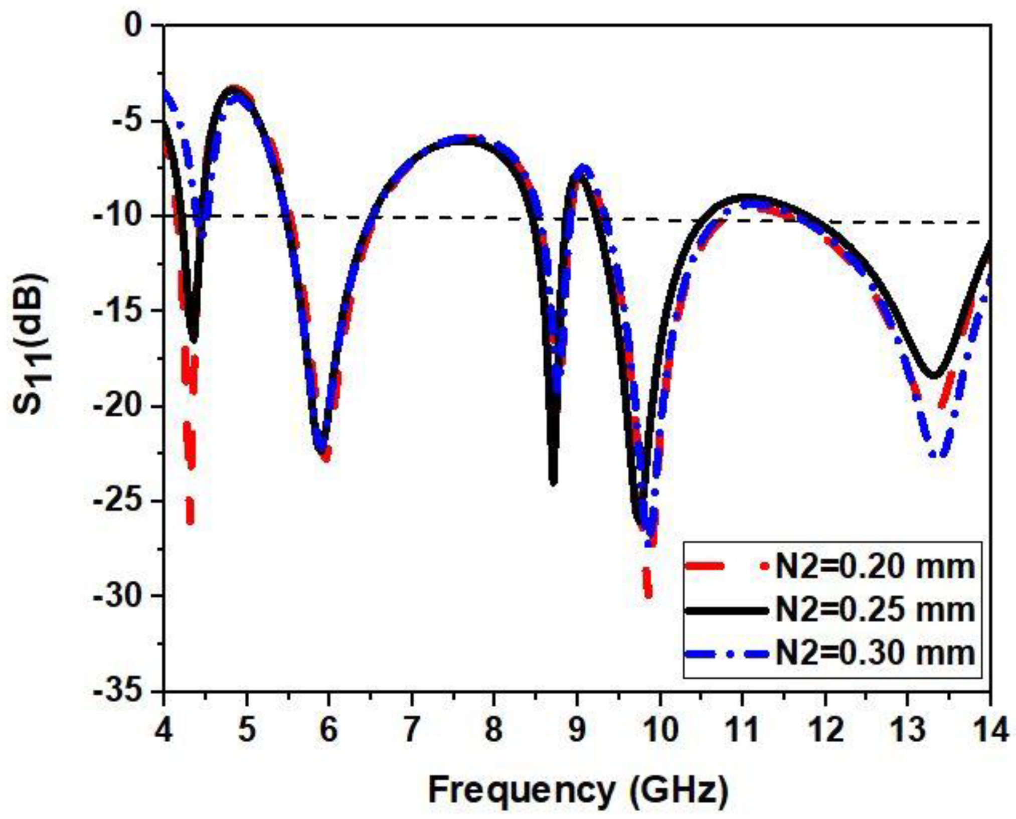
Figure 18.
Parametric analysis for variation in N3 for S11.

Figure 19.
S11 for variation of length ‘N8’.
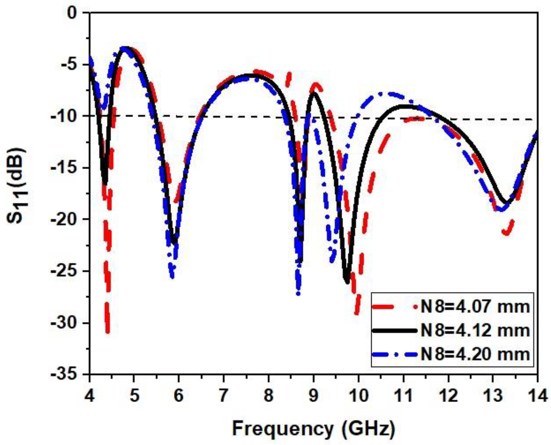
Figure 20.
S11 for variation of length ‘N10’.
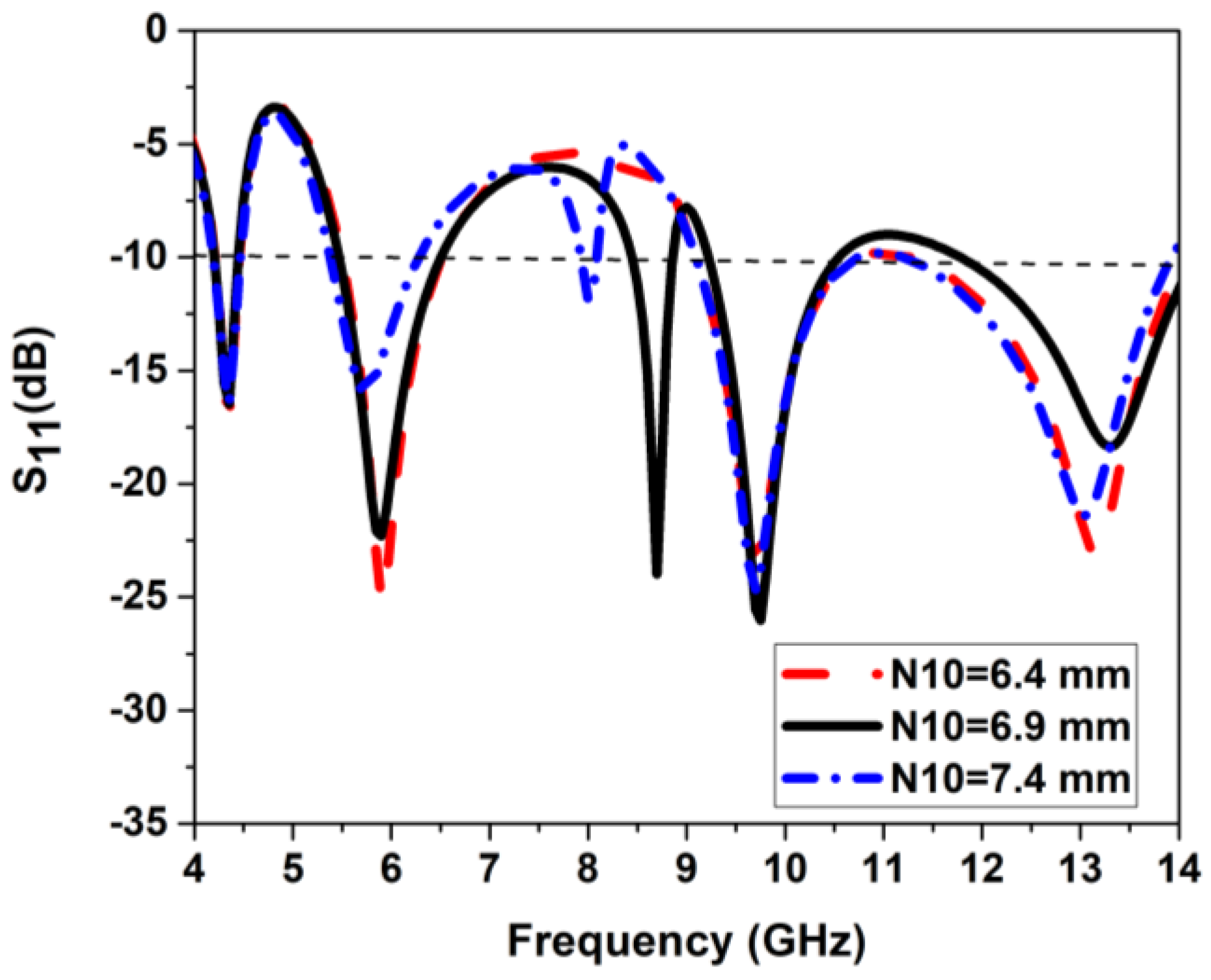
Figure 21.
S11 for variation of length ‘N13’.

Figure 22.
S11 for variation of length ‘N15’.
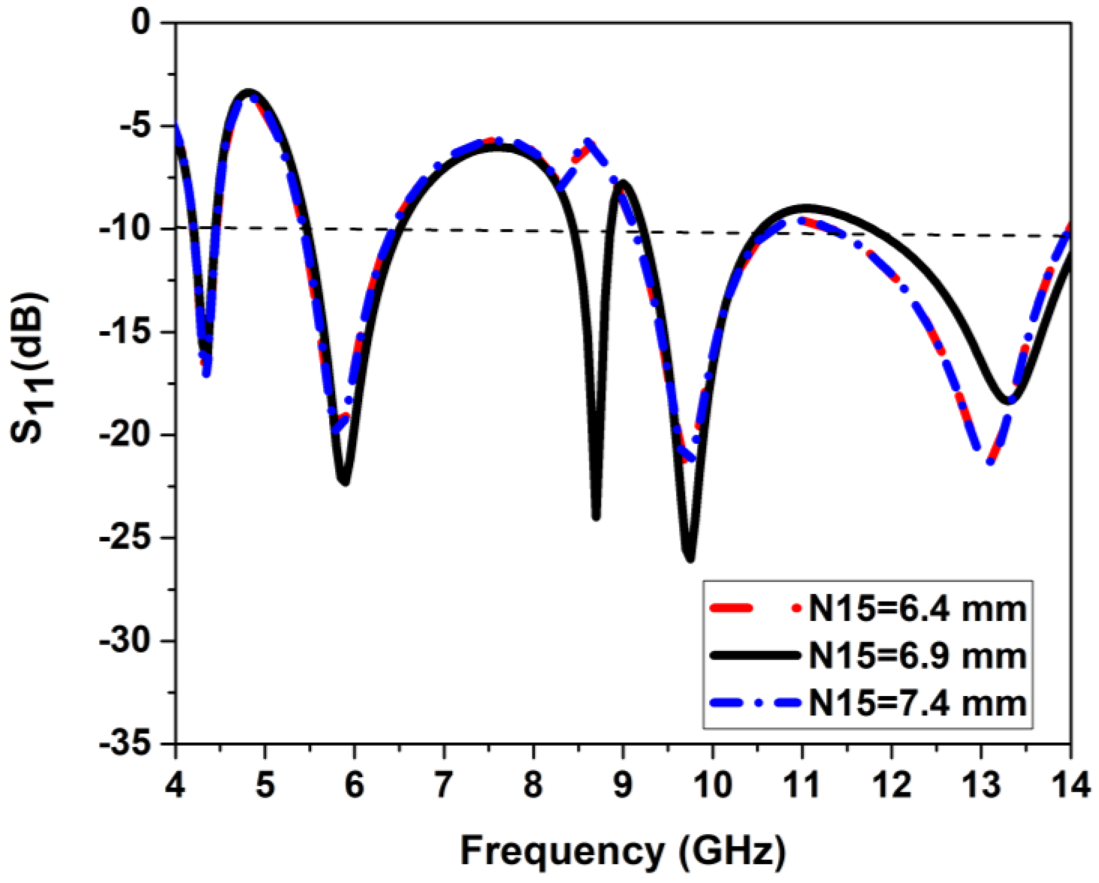
Figure 23.
Surface current at (a) 4.35 GHz, (b) 5.9 GHz, (c) 8.7 GHz, (d) 9.7 GHz.


Figure 24.
Surface current at (a) 4.85 GHz, (b) 7.65 GHz, (c) 9.1 GHz, (d) 11.1 GHz.


Figure 25.
Proposed UWB antenna fabrication: (a) top portion (b) bottom portion.
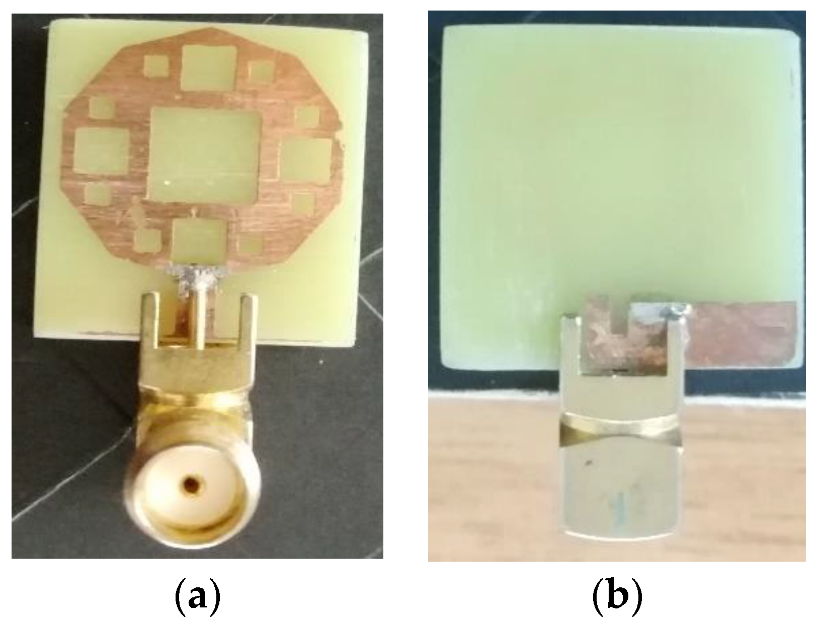
Figure 26.
S11 parameter: simulated and measured.

Figure 27.
Radiation Patterns at (a) 5.8 GHz, (b) 8.7 GHz, (c) 10.95 GHz, (d) 13.25 GHz.
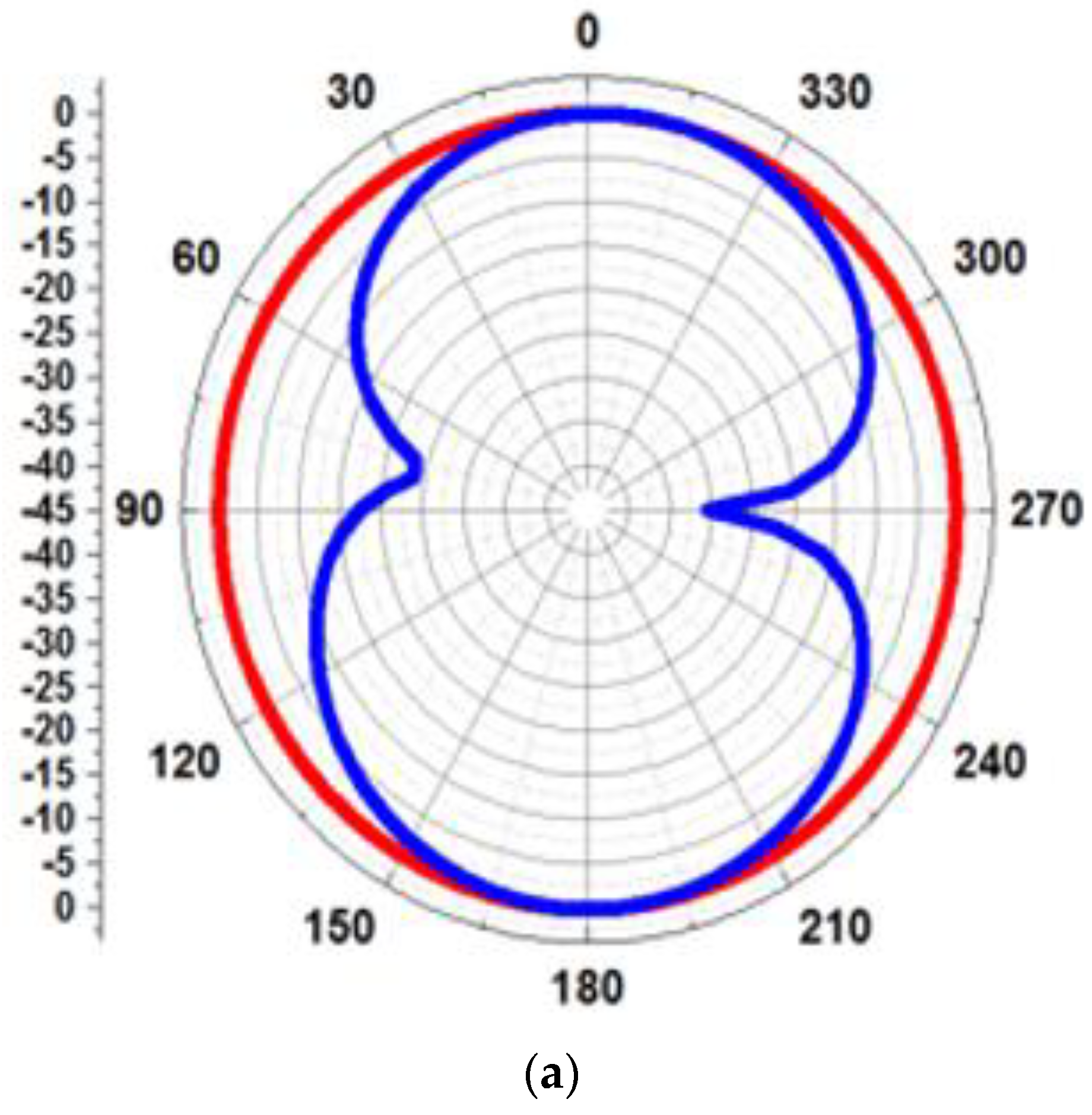
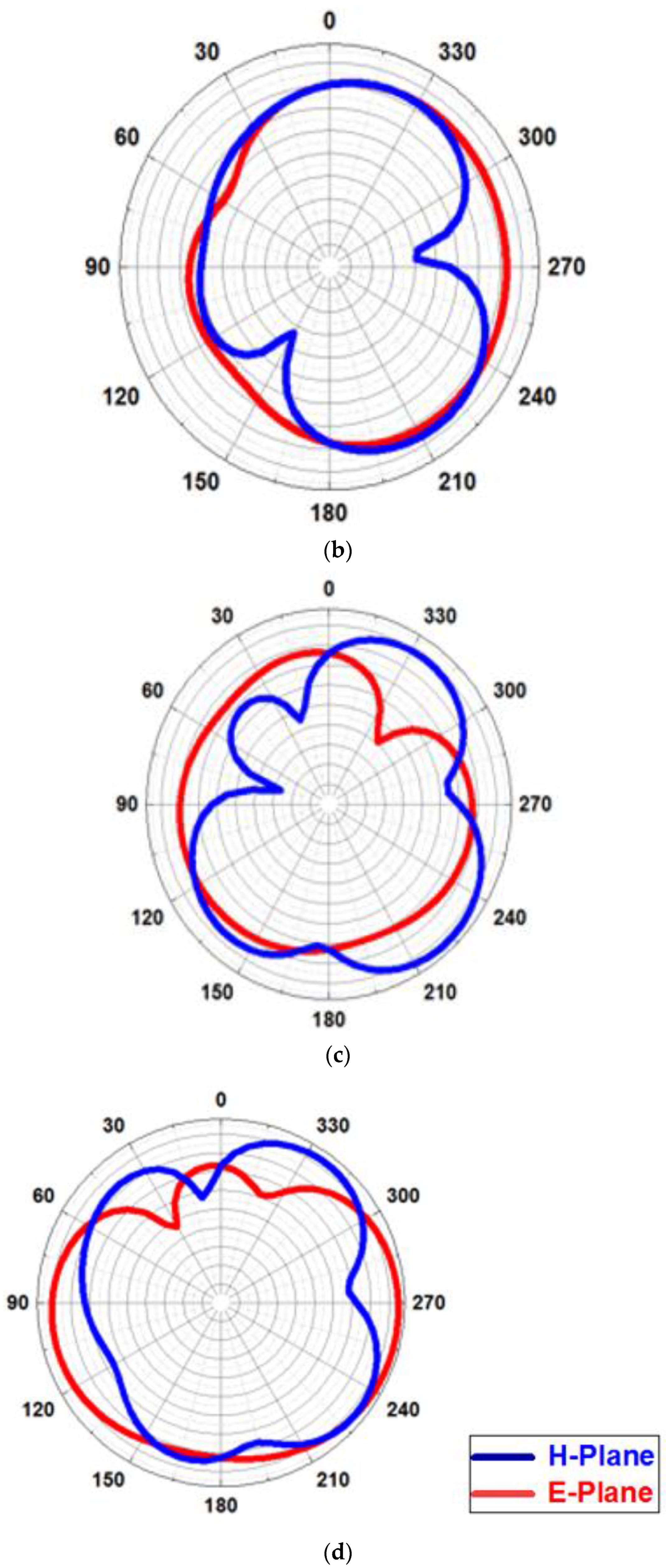
Figure 28.
Analysis in time-domain with (a) frontal and (b) lateral orientations.
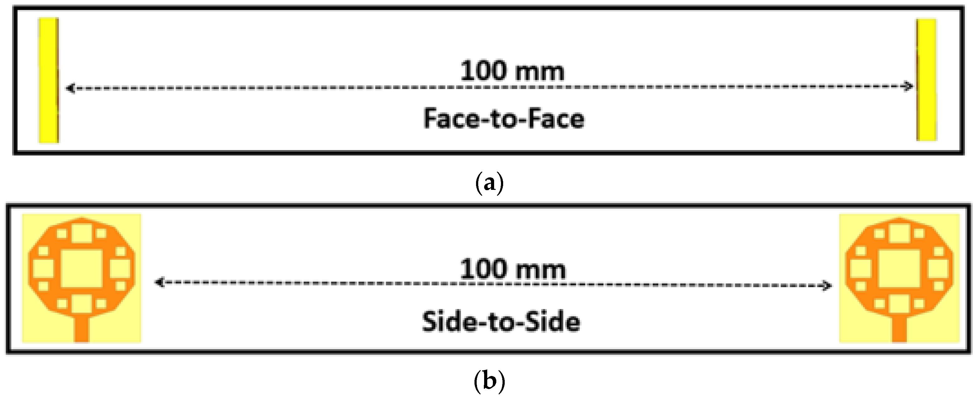
Figure 29.
Group delay.
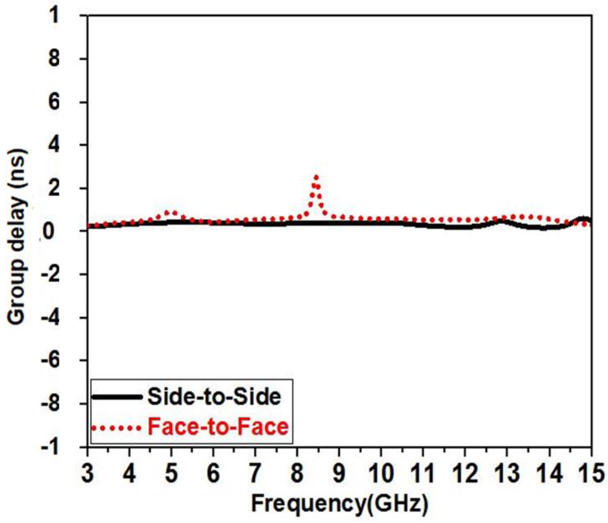
Figure 30.
Isolation.
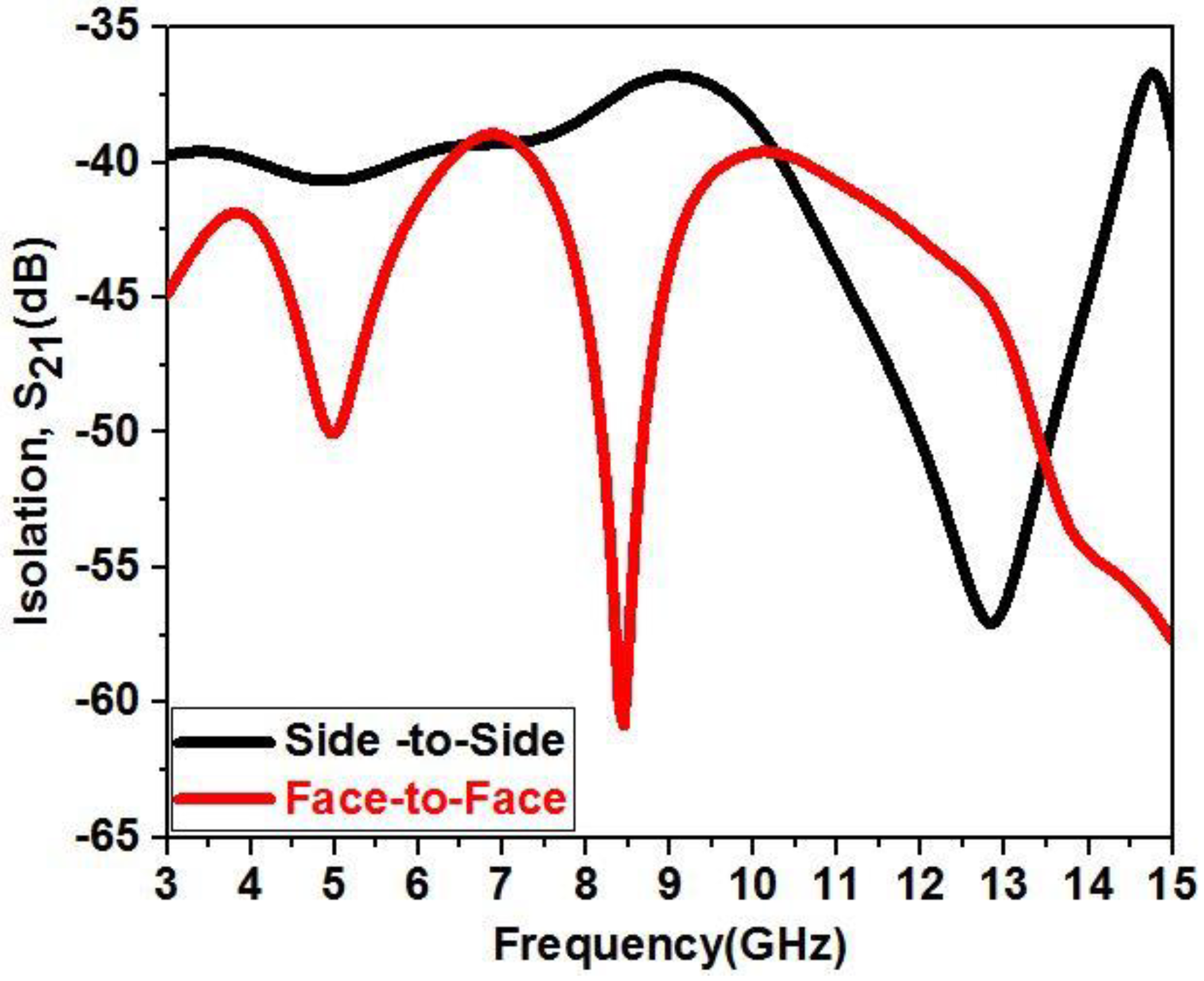
Figure 31.
Phase response S21.

Figure 32.
Simulated Gain.

Figure 33.
The efficiency of the proposed antenna.

Figure 34.
Proposed UWB notch antenna fabrication: (a) top portion (b) bottom portion.
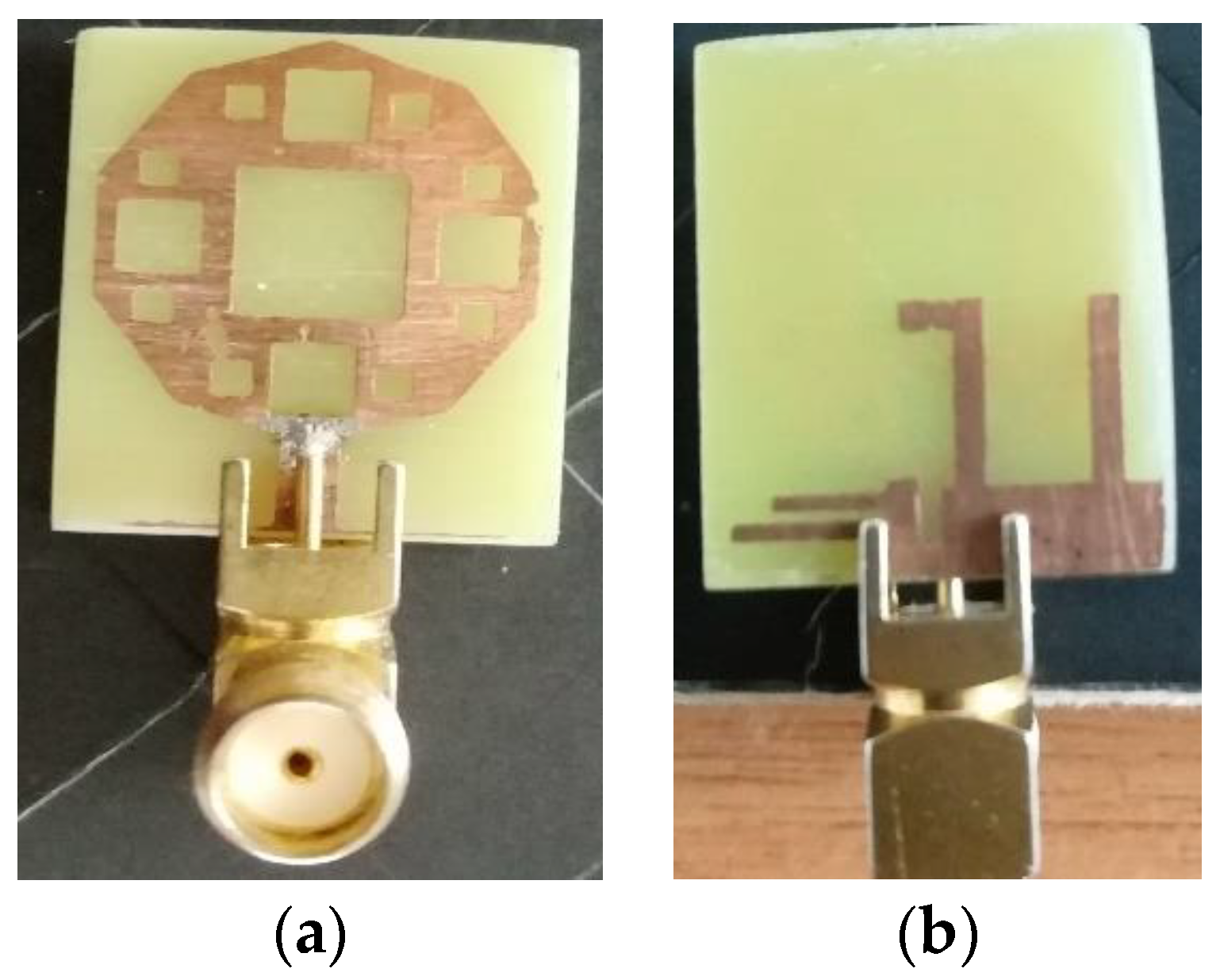
Figure 35.
Simulated and measured S11.

Figure 36.
Radiation Pattern at (a) 4.35 GHz, (b) 5.9 GHz, (c) 8.7 GHz, (d) 9.7 GHz.
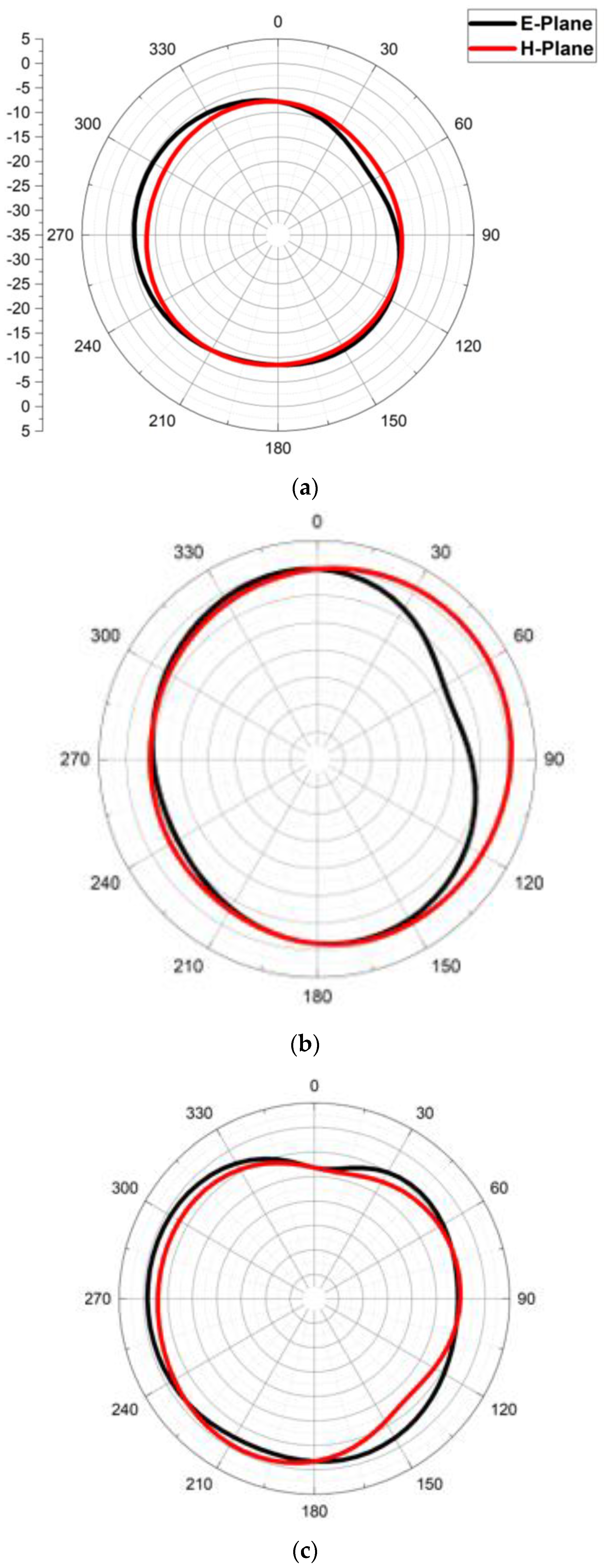

Figure 37.
Analysis in time-domain with (a) frontal and (b) lateral orientations.

Figure 38.
Group delay of notch antenna.

Figure 39.
Isolation.
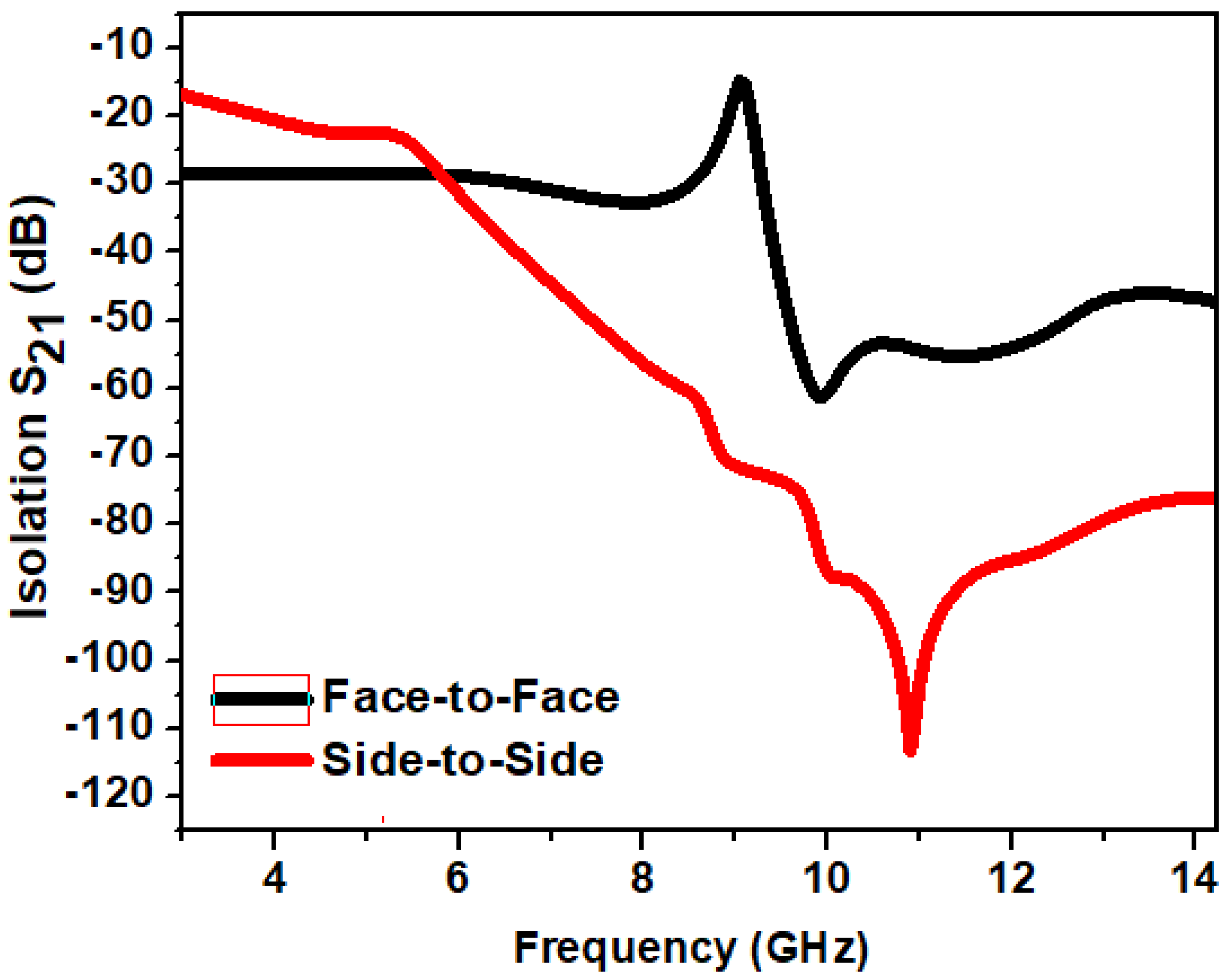
Figure 40.
Phase response S21.


Table 1.
Dimensions of the proposed UWB antenna.
| Parameter | Dimension (mm) | Parameter | Dimension (mm) |
|---|---|---|---|
| W | 17 | S1 | 10 |
| L | 20 | S2 | 3.5 |
| F | 6 | S3 | 1 |
| F1 | 3 | T | 2.5 |
| F2 | 1.5 | T1 | 3.1 |
| LF | 3.82 | A | 15.2 |
| WF | 2 | B | 8.48 |
| S | 1 |
Table 2.
The designed antenna’s dimensions.
| Parameter | Dimension (mm) | Parameter | Dimension (mm) |
|---|---|---|---|
| W | 17 | N7 | 1 |
| L | 20 | N8 | 4.1 |
| F | 6 | N9 | 3.8 |
| F1 | 3 | N10 | 7 |
| F2 | 1.5 | N11 | 8 |
| N1 | 1.75 | N12 | 1 |
| N2 | 0.25 | N13 | 3 |
| N3 | 0.5 | N14 | 1.5 |
| N4 | 5.5 | N15 | 6.9 |
| N5 | 2.1 | N16 | 1 |
| N6 | 5.5 | N17 | 2 |
| Wf | 2 | Lf | 3.82 |
Table 3.
Comparison of proposed UWB notch Antenna Performance with Other Antennas.
| Ref. No. | Size (mm2) | Notch Technique | Range (GHz) | No. of Notch Frequencies | Notch Frequency (GHz) | Phase Response | Group Delay | Transfer Function | Radiation Pattern | Design Complexity | |
|---|---|---|---|---|---|---|---|---|---|---|---|
| E-Plane | H-Plane | ||||||||||
| [24] | 32 × 30 | CSRR and circular stubs | 2.76–11 | 2 | 4.1/6 | linear | linear | <−25 dB | Bidirectional | Omnidirectional | No |
| [25] | 34 × 34 | slot in the feed line | 3.1–10.6 | 1 | 5.5 | linear | linear | NA | Omnidirectional | Omnidirectional | Yes |
| [26] | 18.5 × 39 | Quadratic fractal slot | 3.2–12 | 1 | 5.5 | linear | linear | NA | Bidirectional | Omnidirectional | Yes |
| [27] | 50 × 50 | Slot at the fractal structure | 2.1–11 | 2 | 2.5/5.5 | NA | NA | NA | Bidirectional | Bidirectional | Yes |
| [28] | 42 × 32 | SRR slot | 2.7–14.9 | 2 | 4.9/8.2 | NA | NA | NA | Bidirectional | Omnidirectional | No |
| [29] | 30 × 40 | Shorted stubs in parallel | 2–10.6 | 2 | 3.5/5.2 | NA | NA | NA | Bidirectional | Omnidirectional | Yes |
| [30] | 30 × 30 | Combination of stubs and steeped slots | 2.39–11.4 | 2 | 5.3/5.8 | linear | linear | <−20 dB | Bidirectional | Omnidirectional | Yes |
| [31] | 30 × 40 | Rectangular split ring resonator | 2.4–13.8 | 1 | 5.4 | linear | linear | NA | Bidirectional | Omnidirectional | Yes |
| [32] | 50 × 50 | Fractal Kotch and T-shape slot | 1.7–11 | 3 | 2/3.5/5.8 | NA | NA | NA | Omnidirectional | Bidirectional | No |
| [33] | 24.6 × 38.1 | T-shape slot and Rectangular CSRR | 3–11 | 2 | 3.5/5.5 | linear | linear | NA | Bidirectional | Omnidirectional | No |
| [34] | 30 × 36 | Circular SRR | 2.9–12 | 1 | 3.5 | NA | NA | NA | Omnidirectional | Omnidirectional | No |
| Proposed work | 20 × 17 | Sierpinski square fractal slots | 4.21–13.9 | 4 | 5.05/7.8/9.03/10.86 | linear | linear | <−37 dB | Omnidirectional | Omnidirectional | No |
Disclaimer/Publisher’s Note: The statements, opinions and data contained in all publications are solely those of the individual author(s) and contributor(s) and not of MDPI and/or the editor(s). MDPI and/or the editor(s) disclaim responsibility for any injury to people or property resulting from any ideas, methods, instructions or products referred to in the content. |
© 2023 by the authors. Licensee MDPI, Basel, Switzerland. This article is an open access article distributed under the terms and conditions of the Creative Commons Attribution (CC BY) license (https://creativecommons.org/licenses/by/4.0/).
Share and Cite
MDPI and ACS Style
Kumar, O.P.; Kumar, P.; Ali, T.; Kumar, P.; K, S.B. A Quadruple Notch UWB Antenna with Decagonal Radiator and Sierpinski Square Fractal Slots. J. Sens. Actuator Netw. 2023, 12, 24. https://doi.org/10.3390/jsan12020024
AMA Style
Kumar OP, Kumar P, Ali T, Kumar P, K SB. A Quadruple Notch UWB Antenna with Decagonal Radiator and Sierpinski Square Fractal Slots. Journal of Sensor and Actuator Networks. 2023; 12(2):24. https://doi.org/10.3390/jsan12020024
Chicago/Turabian StyleKumar, Om Prakash, Pramod Kumar, Tanweer Ali, Pradeep Kumar, and Subhash B. K. 2023. "A Quadruple Notch UWB Antenna with Decagonal Radiator and Sierpinski Square Fractal Slots" Journal of Sensor and Actuator Networks 12, no. 2: 24. https://doi.org/10.3390/jsan12020024
Note that from the first issue of 2016, this journal uses article numbers instead of page numbers. See further details here.